JP2012526437A - Demodulator and system for transmitting modulated information, especially for radio frequency identification tags - Google Patents
Demodulator and system for transmitting modulated information, especially for radio frequency identification tags Download PDFInfo
- Publication number
- JP2012526437A JP2012526437A JP2012509006A JP2012509006A JP2012526437A JP 2012526437 A JP2012526437 A JP 2012526437A JP 2012509006 A JP2012509006 A JP 2012509006A JP 2012509006 A JP2012509006 A JP 2012509006A JP 2012526437 A JP2012526437 A JP 2012526437A
- Authority
- JP
- Japan
- Prior art keywords
- frequency
- signal
- period
- delay line
- delay
- Prior art date
- Legal status (The legal status is an assumption and is not a legal conclusion. Google has not performed a legal analysis and makes no representation as to the accuracy of the status listed.)
- Ceased
Links
- 230000001934 delay Effects 0.000 claims abstract description 6
- 238000011144 upstream manufacturing Methods 0.000 claims description 5
- 238000004891 communication Methods 0.000 abstract description 6
- 230000000630 rising effect Effects 0.000 description 34
- 230000003111 delayed effect Effects 0.000 description 15
- 239000003990 capacitor Substances 0.000 description 12
- 230000007704 transition Effects 0.000 description 7
- 230000005540 biological transmission Effects 0.000 description 6
- 230000001360 synchronised effect Effects 0.000 description 6
- 230000010363 phase shift Effects 0.000 description 5
- 238000010586 diagram Methods 0.000 description 4
- 238000000034 method Methods 0.000 description 3
- 230000008901 benefit Effects 0.000 description 2
- 238000006243 chemical reaction Methods 0.000 description 2
- 230000007423 decrease Effects 0.000 description 2
- 238000001514 detection method Methods 0.000 description 2
- 238000005259 measurement Methods 0.000 description 2
- 230000007246 mechanism Effects 0.000 description 2
- 230000004044 response Effects 0.000 description 2
- 230000010354 integration Effects 0.000 description 1
- 230000000737 periodic effect Effects 0.000 description 1
- 230000008569 process Effects 0.000 description 1
- 230000001902 propagating effect Effects 0.000 description 1
Images


Classifications
-
- H—ELECTRICITY
- H04—ELECTRIC COMMUNICATION TECHNIQUE
- H04L—TRANSMISSION OF DIGITAL INFORMATION, e.g. TELEGRAPHIC COMMUNICATION
- H04L27/00—Modulated-carrier systems
- H04L27/10—Frequency-modulated carrier systems, i.e. using frequency-shift keying
- H04L27/14—Demodulator circuits; Receiver circuits
- H04L27/156—Demodulator circuits; Receiver circuits with demodulation using temporal properties of the received signal, e.g. detecting pulse width
- H04L27/1563—Demodulator circuits; Receiver circuits with demodulation using temporal properties of the received signal, e.g. detecting pulse width using transition or level detection
-
- H—ELECTRICITY
- H04—ELECTRIC COMMUNICATION TECHNIQUE
- H04L—TRANSMISSION OF DIGITAL INFORMATION, e.g. TELEGRAPHIC COMMUNICATION
- H04L27/00—Modulated-carrier systems
- H04L27/18—Phase-modulated carrier systems, i.e. using phase-shift keying
- H04L27/22—Demodulator circuits; Receiver circuits
- H04L27/233—Demodulator circuits; Receiver circuits using non-coherent demodulation
- H04L27/2331—Demodulator circuits; Receiver circuits using non-coherent demodulation wherein the received signal is demodulated using one or more delayed versions of itself
-
- H—ELECTRICITY
- H04—ELECTRIC COMMUNICATION TECHNIQUE
- H04L—TRANSMISSION OF DIGITAL INFORMATION, e.g. TELEGRAPHIC COMMUNICATION
- H04L27/00—Modulated-carrier systems
- H04L27/18—Phase-modulated carrier systems, i.e. using phase-shift keying
- H04L27/22—Demodulator circuits; Receiver circuits
- H04L27/233—Demodulator circuits; Receiver circuits using non-coherent demodulation
- H04L27/2335—Demodulator circuits; Receiver circuits using non-coherent demodulation using temporal properties of the received signal
Landscapes
- Engineering & Computer Science (AREA)
- Computer Networks & Wireless Communication (AREA)
- Signal Processing (AREA)
- Digital Transmission Methods That Use Modulated Carrier Waves (AREA)
Abstract
本発明は、無線通信および特にRFID(無線周波数識別)タイプの近距離無線通信システムに関する。
RFIDタグにおける局部クロック発生器を必要とせずに、周波数変調または位相変調モードで動作するために、本発明は、新規の復調器であって、入力信号の周期に等しいかまたはその周期に非常に近い期間を備えたシンボルによって位相または周波数変調された入力周波数(Hs)の入力信号を受信するのに適した遅延線(DEL)を含む新規の復調器を提案する。遅延線は、入力周波数における、しかし互いに対してΔTだけオフセットされたNdの異なる遅延を備えたNd信号を生成するNd出力部を有し、Ndは、1以上の整数である。復調器はまた、Ndラッチ、すなわちそれぞれが、遅延線のそれぞれの出力、および入力信号からなるクロック信号を受信するNdラッチのレジスタを含んで、入力信号の周期の終わりにおける遅延線の出力の状態をラッチレジスタに記憶するようにする。レジスタの内容は、入力信号変調シンボル(SY)の値を表す。
【選択図】 図2The present invention relates to wireless communication and in particular to a near field wireless communication system of the RFID (Radio Frequency Identification) type.
In order to operate in frequency modulation or phase modulation mode without the need for a local clock generator in the RFID tag, the present invention is a novel demodulator that is equal to or very much in period of the input signal. A novel demodulator is proposed that includes a delay line (DEL) suitable for receiving an input signal of an input frequency (H s ) that is phase or frequency modulated by a symbol with a near period. Delay line at the input frequency, but has an N d output section for generating a N d signals having a N d different delays that are offset ΔT with respect to one another, N d is an integer of 1 or more. Demodulator also, N d latches, i.e., respectively, the respective outputs of the delay line, and a register of N d latch which receives a clock signal and an input signal, the delay line at the end of the period of the input signal output This state is stored in the latch register. The contents of the register represent the value of the input signal modulation symbol (SY).
[Selection] Figure 2
Description
本発明は、無線通信および特にRFID(無線周波数識別タイプ)の近距離無線通信システムに関する。 The present invention relates to wireless communication and in particular to RFID (Radio Frequency Identification Type) near field communication systems.
RFIDシステムによって、データは、リーダと小さな寸法のタグとの間の非常に短い距離(数センチメートルから数メートル、または例外的にさらに長く)にわたって送信することが可能になる。リーダは、エネルギおよび情報(例えば、問い合わせ)をタグに搬送する無線周波数で信号を送信する。タグは、受信したエネルギによって作動され、かつ受信した情報または問い合わせに応じて情報をリーダに送信する。情報は、タグおよびしたがって間接的にはタグが装着された対象物の単純な数値識別であってもよい。タグには、無線アンテナ、すなわち、リーダによって送信された周波数の信号を受信できるようにする、かつ応答としてリーダに送信される情報によって変調された無線信号を返送できるようにする無線アンテナが含まれる。変調は、この目的のために集積回路チップを含み得るタグにおいて行われる。時としてタグには、補助機能を扱うためのバッテリが設けられるが、しかし、通常、タグの機能が主に識別機能である場合に、タグは、リーダから受信される無線周波数エネルギによって完全に電力が供給される。 RFID systems allow data to be transmitted over a very short distance (a few centimeters to a few meters, or exceptionally longer) between a reader and a small sized tag. The reader transmits a signal at a radio frequency that carries energy and information (eg, an inquiry) to the tag. The tag is activated by the received energy and sends information to the reader in response to the received information or inquiry. The information may be a simple numerical identification of the tag and thus indirectly the object to which the tag is attached. The tag includes a wireless antenna, i.e., a wireless antenna that allows reception of a signal at a frequency transmitted by the reader and returns a wireless signal modulated by information transmitted to the reader in response. . Modulation is performed on a tag that may include an integrated circuit chip for this purpose. Sometimes a tag is provided with a battery to handle auxiliary functions, but usually the tag is completely powered by radio frequency energy received from the reader when the tag function is primarily an identification function. Is supplied.
リーダによって実行される変調は、通常、搬送波周波数の振幅変調であるが、しかし、今はまた、周波数または位相変調を行って、より高い情報ビットレートを可能にする努力がなされている。タグによって実行される変調は、負荷変調、すなわちアンテナインピーダンスの変調であってもよく、この変調は、リーダの送信/受信アンテナのインピーダンスに作用する。ここでの関心は、主として、リーダによって行われる変調、およびタグによって行われる復調に集中する。 The modulation performed by the reader is usually amplitude modulation of the carrier frequency, but now also efforts are being made to perform frequency or phase modulation to allow higher information bit rates. The modulation performed by the tag may be load modulation, ie, antenna impedance modulation, which affects the impedance of the reader's transmit / receive antenna. The focus here is mainly on the modulation performed by the reader and the demodulation performed by the tag.
リーダによる変調が、中心搬送波周波数F0を備えた信号の周波数または位相変調である場合に、タグにおいて情報を復調できることが必須であり、かつそのために、タグにおいて同じ中心周波数F0の信号を有することが必須である。周波数または位相変調モードで動作する通常の無線通信システムにおいて、受信機は、一般に、復調されることになる無線周波数信号の中心周波数に合わせられた局部周波数発生器を有する。局部発生器は、中間周波数またはベースバンドへの周波数変換によって復調を行う。復調器はまた、局部電圧制御発振機(VCO)から信号を受信する、かつこの信号の周波数を受信周波数に合わせる位相ロックループを用いることができる。非常に特有なタイプの変調を用いれば、時として局部発振器を省くことが可能であるが、しかしこれは、一般的な場合には可能ではない。 If the modulation by the reader is a frequency or phase modulation of a signal with a center carrier frequency F 0 , it is essential that the information can be demodulated at the tag, and therefore has a signal with the same center frequency F 0 at the tag It is essential. In a typical wireless communication system operating in frequency or phase modulation mode, the receiver typically has a local frequency generator tuned to the center frequency of the radio frequency signal to be demodulated. The local generator performs demodulation by frequency conversion to an intermediate frequency or baseband. The demodulator can also use a phase locked loop that receives a signal from a local voltage controlled oscillator (VCO) and matches the frequency of this signal to the received frequency. With a very specific type of modulation it is sometimes possible to omit the local oscillator, but this is not possible in the general case.
今日、RFIDタグには、この周波数発生器またはこの局部発振器用の多くのスペースがなく、それらを動作させるために利用可能な多量のエネルギがない。集積回路チップに基づいた制御周波数局部発振器またはスタンドアロン周波数発生器は、一般に、チップ外の構成要素を必要とし、かかる外部構成要素をタグに有することは、容積の理由で望ましくない。 Today, RFID tags do not have much space for this frequency generator or this local oscillator and there is not a large amount of energy available to operate them. Controlled frequency local oscillators or stand-alone frequency generators based on integrated circuit chips generally require components outside the chip, and having such external components in the tag is undesirable for volume reasons.
したがって、本発明の目的は、リーダとRFIDタグとの間の通信に特に適している、情報を送信するためのシステムおよび対応する電子復調回路を提案することである。このシステムは、復調器における局部周波数発生器の必要なしに、かつタグに存在する単一の集積回路チップに追加されることになる外部構成要素なしに、周波数または位相変調位相で送信することができる。 The object of the present invention is therefore to propose a system for transmitting information and a corresponding electronic demodulation circuit which are particularly suitable for communication between a reader and an RFID tag. This system can transmit in frequency or phase modulation phase without the need for a local frequency generator in the demodulator and without external components that would be added to a single integrated circuit chip present in the tag. it can.
本発明による送信システムにおいて、可変であるが、しかし受信無線周波数信号の周期に関連づけられている期間用に、搬送波の周波数または位相を修正する変調のための準備が、第1になされる。情報は、特定の周波数または位相によってそれぞれが表される一連の隣接する「シンボル」からなり、シンボルは、この周波数またはこの位相と関連する期間を測定することによって検出される。各可能なシンボルは、例えばNs周期続き、Nsは、全てのシンボルに対して同じである固定整数であるが、しかし(周波数変調モードにおける)周波数または(位相変調モードにおける)位相は、シンボルに従って変化する。復調は、Ns周期のグループの期間を決定して、そこから変調の周波数または位相を推定することに存し、したがってシンボルの値は、Ns周期のこのグループに対応する。 In a transmission system according to the invention, provisions are first made for modulation that modifies the frequency or phase of the carrier for a period that is variable, but is associated with the period of the received radio frequency signal. Information consists of a series of adjacent “symbols” each represented by a particular frequency or phase, which is detected by measuring the period associated with this frequency or this phase. Each possible symbol lasts for example N s periods, where N s is a fixed integer that is the same for all symbols, but the frequency (in frequency modulation mode) or phase (in phase modulation mode) is the symbol Changes according to Demodulation consists in determining the duration of a group of N s periods from which the frequency or phase of the modulation is estimated, so that the value of the symbol corresponds to this group of N s periods.
周波数変調モードにおいて、シンボル期間は、変調信号FのNs周期と正確に等しいのが好ましい。位相変調モードにおいて、シンボル期間はまた(この期間は、位相に依存する)、シンボルの全体的な期間が変調に従って変化するように、位相変調された搬送波周波数F0のNs周期に等しいのが好ましい。中心周波数F0のまわりの周波数変調指数(Fmin−Fmax)/F0が十分に低いならば適用できる可能な変形において、シンボル期間は、一定だが、しかし中心周波数F0における信号のNs周期に等しいかまたは非常に近くすることができ、復調は、もう一度変調信号のNs周期の期間を遵守することに存する。 In the frequency modulation mode, symbol period is preferably equal exactly the N s period of the modulation signal F. In phase modulation mode, the symbol period (which depends on the phase) is also equal to the N s period of the phase modulated carrier frequency F 0 so that the overall period of the symbol changes according to the modulation. preferable. In a possible variation that can be applied if the frequency modulation index (F min −F max ) / F 0 around the center frequency F 0 is sufficiently low, the symbol period is constant, but the N s of the signal at the center frequency F 0 . can be equal to or very close to the period, demodulation consists in compliance with the period of N s cycle again modulated signal.
このタイプの変調は、中心周波数F0におけるどんなローカルクロックも必要としない本発明による復調器によって復調することができる。復調器には、入力信号の周期に等しいかまたはその周期に非常に近い期間を備えたシンボルによって位相または周波数変調された、入力周波数の入力信号を受信するのに適した遅延線が含まれるが、この遅延線は、入力信号の周波数における、しかしNdの異なる遅延を備えたNd信号を生成するNd出力部を有し、Ndは、1以上の整数であり、復調器は、Ndラッチであって、それぞれが、一方では遅延線のそれぞれの出力を受信し、他方では入力信号からなるクロック信号を受信するNdラッチのレジスタを含んで、入力信号の周期の終わりにおける遅延線の出力の状態をラッチレジスタに記憶するようにし、レジスタの内容が、入力信号変調シンボルの値を表す。 This type of modulation can be demodulated by the demodulator according to the present invention that any not local clocks required at the center frequency F 0. The demodulator includes a delay line suitable for receiving an input signal at the input frequency, phase or frequency modulated by a symbol with a period equal to or very close to the period of the input signal. the delay line at the frequency of the input signal, but has a N d output section for generating a N d signals with different delays N d, N d is an integer of 1 or more, the demodulator, a N d latches, respectively, on the one hand receives the output of each delay line, on the other hand a register of N d latch which receives a clock signal and an input signal, the delay at the end of the period of the input signal The output state of the line is stored in the latch register, and the contents of the register represent the value of the input signal modulation symbol.
遅延線は、固定遅延を備えた線であってもよい。しかしながら、線の異なる出力部において確立された遅延増分が、1つのシンボルから次のシンボルへと安定したままであるが、しかし入力信号の平均周波数へと長期的に平均して調整されるように、遅延線が、(シンボル期間を与えられたとすると)長い時定数を備えたロックループによって制御されるのが好ましい。このロッキングは、以下でより詳細に説明する。次に、ロックループは、一方では入力周波数で入力信号を受信し、かつ他方では遅延線の出力の1つを受信する位相比較器と、シンボル期間よりはるかに大きい時定数を備えた積分器と、を含むのが好ましく、積分器の出力は、遅延線によって確立された遅延増分の期間を制御して、それらを、入力周波数の平均値に従ってロックするようにする。 The delay line may be a line with a fixed delay. However, the delay increments established at the different outputs of the line remain stable from one symbol to the next, but are adjusted on an average over time to the average frequency of the input signal. The delay line is preferably controlled by a locked loop with a long time constant (assuming a given symbol period). This locking is described in more detail below. Next, the lock loop includes a phase comparator that, on the one hand, receives the input signal at the input frequency and on the other hand receives one of the outputs of the delay line, and an integrator with a time constant much larger than the symbol period; , And the output of the integrator controls the period of delay increments established by the delay line so that they lock according to the average value of the input frequency.
復調器は、周波数を整数Nsで割る周波数分割器を遅延線の上流に含むのが好ましい。この分割器は、位相または周波数変調された無線周波数の信号を受信することに、および無線周波数よりNs倍低い変調された入力周波数の入力信号を遅延線の入力部に供給することに適している。 Demodulator preferably comprises a frequency divider dividing the frequency by an integer N s upstream of the delay line. The divider to receive a signal of a phase or frequency modulated radio frequency, and adapted to supply an input signal of N s times lower modulated input frequency from the radio frequency to the input of the delay line Yes.
本発明による復調器は、リーダおよびタグを含む送信システムにおいて使用できるが、この送信システムにおいて、リーダは、周波数または位相変調モードで送信し、かつシンボルは、同期して(すなわち、変調された無線信号の固定周期数を表す期間で)または非同期で(非変調中心周波数における信号の固定周期数を好ましくは表す固定期間で)送信される。 The demodulator according to the invention can be used in a transmission system comprising a reader and a tag, in which the reader transmits in frequency or phase modulation mode and the symbols are synchronized (ie modulated radio). Transmitted in a period representing a fixed number of periods of the signal) or asynchronously (in a fixed period preferably representing the number of fixed periods of the signal at the unmodulated center frequency).
本発明の他の特徴および利点は、添付の図面に関連して提供される、以下の詳細な説明を読むことで明らかになろう。 Other features and advantages of the present invention will become apparent upon reading the following detailed description, provided in conjunction with the accompanying drawings.
図1は、それぞれSY0、SYa、SYbで示された、異なる値の連続シンボルによって周波数変調された中心無線周波数からなる無線周波数信号を示す。シンボルの値は、このシンボルに割り当てられたそれぞれの周波数F(F=F0、Fa、Fb...)によって定義される。図1は、非変調基本周波数と同様に、より高い変調周波数Faおよびより低い変調周波数Fbを示す。 FIG. 1 shows a radio frequency signal consisting of a central radio frequency, frequency-modulated by successive symbols of different values, denoted SY 0 , SY a , SY b respectively. The value of the symbol is defined by the respective frequency F (F = F 0 , F a , F b ...) Assigned to this symbol. FIG. 1 shows a higher modulation frequency F a and a lower modulation frequency F b as well as an unmodulated fundamental frequency.
変調期間、すなわちその間に信号が送信される期間は、無線周波数信号の周期にリンクされる。 The modulation period, i.e. the period during which signals are transmitted, is linked to the period of the radio frequency signal.
図1に示す最も単純な場合に、シンボル期間は、固定数の信号周期、好ましくは整数Nsに等しい。したがって、シンボルの値は、送信される信号の周波数の値によってだけでなく、シンボルのそれぞれの期間によって表され、この期間は、T=Ns/F、すなわちT0=Ns/F0、Ta=Ns/Fa、Tb=Ns/Fb等である。図1の例において、原理をよりよく理解できるようにするために、Ns=4であり、周波数変動は、故意に誇張された。 In the simplest case shown in FIG. 1, symbol period, the signal period of the fixed number, preferably equal to an integer N s. Thus, the value of the symbol is represented not only by the value of the frequency of the transmitted signal but also by the respective period of the symbol, this period being T = N s / F, ie T 0 = N s / F 0 , T a = N s / F a , T b = N s / F b and the like. In the example of FIG. 1, in order to better understand the principle, N s = 4 and the frequency variation was deliberately exaggerated.
この単純な場合に、シンボル期間は、Ns周期と正確に等しく、Ns周期は、全て同一である期間を有する。復調は、正確にNs同一周期の期間であるシンボル期間を測定するために遅延線を用いることに存する。本発明がまた、以下の場合に適用可能であることが後で分かる。
− シンボル期間が変調信号のNs周期に等しく、この期間が位相に依存する位相変調の場合。
− シンボル期間が、無線信号における平均周波数F0のNs周期に好ましくは等しい共通値T0と全て同一である非同期変調の場合。
If this simple, symbol period, N s cycle and exactly equal, N s period, all have period are the same. Demodulation consists in the use of delay lines in order to accurately measure the symbol period is a period of N s identical period. It will be seen later that the present invention is also applicable in the following cases.
- equal to N s periods of the symbol duration modulation signal, if this period is the phase modulation depends on the phase.
In the case of asynchronous modulation where the symbol period is all identical to the common value T 0 , preferably equal to the N s period of the average frequency F 0 in the radio signal
全ての場合に、変調は、次のように行われる。すなわち、シンボル期間が、正確に変調信号のNs周期(期間1/FのNs同一周期、もしくは必ずしも同一でないが期間の合計が位相に依存するNs周期)であるか、さもなければ平均周波数F0のNs周期であるかどうかにかかわらず、シンボル期間が、無線周波数信号における整数Nsの周期を表すように行われる。全ての場合に、変調信号のNs周期の期間が測定される。
In all cases, the modulation is performed as follows. I.e., symbol period is a N s period of exactly modulated signal (N s period N s identical period of
図2は、これらの異なる方法の1つで変調された信号を復調するための、本発明による復調器の実施形態を表す。それには、タグのアンテナ(図示せず)から得られた、復調される無線周波数RFを受信する入力部E1が含まれる。入力部E1は、受信信号の周波数Fを数Nsで割る、かつNs/Fに等しい周期を備えた、入力信号と呼ばれる代替信号Hsを出力部で生成する周波数分割器DIV(実際にはカウンタ)の入力部にリンクされる。カウンタ/分割器は、オプションである。その存在は、予想される変調に依存する。シンボル期間が、(上記のように、正確にまたはおおむね)無線周波数信号のNs周期(Ns>1)を表すように、変調が行われる場合に、Nsによる分割器が必要である。しかしながら、Nsは、限界において1に等しくなることができ、変調は、無線周波数信号の各新しい周期において行われ、この場合に、分割器の必要はない。 FIG. 2 represents an embodiment of a demodulator according to the invention for demodulating a signal modulated in one of these different ways. It includes an input E1 that receives a demodulated radio frequency RF obtained from a tag antenna (not shown). The input unit E1 divides the frequency F of the received signal by a number N s and has a period equal to N s / F and generates a substitute signal H s called an input signal at the output unit, which is a frequency divider DIV (actually Are linked to the input of the counter). A counter / divider is optional. Its presence depends on the expected modulation. If the modulation is performed such that the symbol period represents the N s period (N s > 1) of the radio frequency signal (as described above, exactly or roughly), a N s divider is required. However, N s can be equal to 1 at the limit, and the modulation is performed in each new period of the radio frequency signal, in which case there is no need for a divider.
したがって、本発明による復調器のコアは、分割器の後に位置する。復調器のコアの入力部は、分割器の出力部にリンクされた入力部E2であり、この入力部は、信号Hsを受信するが、その周波数はNsで割られた周波数Fである。 Therefore, the core of the demodulator according to the invention is located after the divider. The input of the demodulator core is an input E2 linked to the output of the divider, which receives the signal H s , whose frequency is the frequency F divided by N s. .
入力部E2は、数Ndの出力部S1〜SNdを有する遅延線DELの入力部であり、各出力部Siは、入力信号Hsと同じ周期だがそれぞれの遅延Diを備えた信号を供給し、ここでiは、リンクにおける出力部のランクを表す添え字である。Nd出力の遅延Diは、最小値と最大値との間の間隔ΔTで規則的にフェーズされる。
Input unit E2 is an input section of the delay line DEL having an
遅延線は、固定値ΔTによってフェーズされた固定遅延を生成する線とすることができる。しかしながら、基本遅延ΔTの値が、復調器によって受信される信号の平均周波数F0にロックされるのが好ましい。実際には、値ΔTは、受信された平均周波数に近い信号周期期間の間の偏差を測定するために用いられ、受信された平均周波数と、偏差を測定する際に用いられる遅延値との間に直接リンクが存在することが望ましい。 The delay line may be a line that generates a fixed delay phased by a fixed value ΔT. However, the value of the basic delay ΔT is preferably locked to the average frequency F 0 of the signal received by the demodulator. In practice, the value ΔT is used to measure the deviation between signal period periods close to the received average frequency, and between the received average frequency and the delay value used in measuring the deviation. It is desirable for a direct link to exist.
この理由で、図2は、かかるロックキング機構を設けられた復調器を表す。ロッキングは、位相比較器CMPHと、復調されるシンボル期間と比較して長い時定数(好ましくは、時定数は、シンボル期間の少なくとも数百倍である)を備えた積分器と、を含む位相ロックループによってもたらされる。 For this reason, FIG. 2 represents a demodulator provided with such a locking king mechanism. The locking includes a phase comparator CMPH and an integrator with a time constant that is long compared to the demodulated symbol period (preferably the time constant is at least several hundred times the symbol period). Brought by the loop.
位相比較器は、一方では入力周波数Hsの入力信号を受信し、他方では遅延線の出力部の1つ(出力部Sm)から信号を受信する。出力部Smは、基準遅延Dmを備えた信号Hsを、次のように供給する。すなわち、平均変調周波数F0/Nsに関して、出力部Smにおける信号の立ち上がりエッジが、非遅延信号Hsの立ち上がりエッジと同相(これは、位相比較器の構造に依存して、位相対立になる可能性がある)であるように、供給する。 Phase comparator, on the one hand, receives an input signal of the input frequency H s, on the other hand receives signals from one of the outputs of the delay line (output unit S m). The output unit S m supplies the signal H s with the reference delay D m as follows. That is, with respect to the average modulation frequency F 0 / N s , the rising edge of the signal at the output unit S m is in phase with the rising edge of the non-delayed signal H s (this depends on the phase comparator, depending on the phase comparator structure). To be).
位相ロックループは、出力Smを入力E2と同相に保つ傾向がある方向において基本遅延ΔTを調整することによって遅延線に作用する(したがって、位相比較器の入力部間のゼロ位相シフト)。ループの高い時定数によって、この位相整列を、無線信号の平均周波数F0用に行うことが可能になる。これゆえに、遅延期間ΔTは、シンボルからシンボルへと固定されていると考えることができる。 The phase locked loop acts on the delay line by adjusting the basic delay ΔT in a direction that tends to keep the output S m in phase with the input E2 (thus, a zero phase shift between the inputs of the phase comparator). The high time constant of the loop makes it possible to perform this phase alignment for the average frequency F 0 of the radio signal. Therefore, it can be considered that the delay period ΔT is fixed from symbol to symbol.
位相比較器の出力部に配置された積分器は、例えば、電荷ポンプPCHおよび積分器(コンデンサCint)を用いて構成される。コンデンサCintの端子における積分電圧は、遅延線の制御入力部Ecに印加される。この入力部における電圧は、基本遅延ΔTの値に、したがって遅延線によって確立される全ての遅延に作用する。位相比較器CMPHによって提供された位相シフト情報の積分ゆえに、積分コンデンサの端子における電圧は、信号HsとSmにおける出力信号との間の平均位相シフトがゼロ(または一定)になるような値で安定化される。 The integrator disposed at the output unit of the phase comparator is configured using, for example, a charge pump PCH and an integrator (capacitor C int ). Integrated voltage at the terminals of the capacitor C int is applied to the control input E c of the delay line. The voltage at this input affects the value of the basic delay ΔT and thus all delays established by the delay line. Due to the integration of the phase shift information provided by the phase comparator CMPH, the voltage at the terminal of the integrating capacitor is such that the average phase shift between the signal H s and the output signal at S m is zero (or constant). Stabilized.
遅延線のNd出力は、多数のラッチDを備えたレジスタDFFの入力部に印加される。各ラッチDは、その入力部Dにおいて、Nd出力のそれぞれの出力を受信し、かつクロック入力部CLKにおいて、周波数F/Nsの入力信号Hsを受信する。信号Hsの立ち上がりエッジ(例えば)に基づいて、ラッチは、それぞれ、それらのそれぞれの入力部Dに課された状態を取る。この状態は、出力部のそれぞれにおいて異なって遅延された、第1の立ち上がりエッジ後におけるHsの第2の立ち上がりエッジの到着の瞬間に依存する。第1の立ち上がりエッジは、シンボルの開始を定義するエッジである。第2の立ち上がりエッジは、シンボルの終わり(および新しいシンボルの開始)を定義するエッジである。シンボルの終わりにおいて、ラッチレジスタのNd出力セットは、温度計型符号に従って、ちょうど終了したシンボルを表す値を定義する。 The Nd output of the delay line is applied to the input of a register DFF having a number of latches D. Each latch D at its input D, receives the respective outputs of N d outputs, and the clock input CLK, and receives an input signal H s of the frequency F / N s. Based on the rising edge of the signal H s (for example), the latch, respectively, take their imposed on respective inputs D state. This state depends on the instant of arrival of the second rising edge of H s after the first rising edge, which is delayed differently in each of the outputs. The first rising edge is the edge that defines the start of the symbol. The second rising edge is the edge that defines the end of the symbol (and the start of a new symbol). At the end of the symbol, the Nd output set of the latch register defines a value representing the symbol that just ended according to the thermometer type code.
ラッチレジスタの出力部に配置された符号化回路CODによって、例えば2進符号に従い、温度計以外の形態でシンボルの値を供給することが可能になる。連続シンボルは、Hsの立ち上がりエッジの到着と共に出力部SYに到着する。 The encoding circuit COD arranged at the output of the latch register makes it possible to supply symbol values in a form other than a thermometer, for example, according to a binary code. Successive symbols arrive at the output unit SY with the arrival of the rising edge of H s.
図3は、受信信号の変調が周波数変調であり、かつ各シンボルが、復調器の入力部E1で受信された無線信号RFのNs周期(図3ではNs=4)と正確に等しい期間を有する例で復調を説明するタイミング図を表す。3つの連続シンボルSY0、SYa、SYbが表されており、それぞれ3つの異なる周波数値F0、Fa、Fbに、およびしたがって3つの異なる期間に対応する。周波数F0が、中心周波数、すなわちそのまわりで変調が実行される中心周波数であること、およびこの周波数F0が、変調信号の平均周波数であることが、ここで仮定されている。周波数FaはF0より高く、周波数FbはF0より低い。この例では、シンボルSY0は、平均周波数F0に割り当てられているが、しかしこれは、必須ではない。 FIG. 3 shows a period in which the modulation of the received signal is frequency modulation and each symbol is exactly equal to the N s period (N s = 4 in FIG. 3) of the radio signal RF received at the input E1 of the demodulator. A timing diagram illustrating demodulation is shown in an example having Three consecutive symbols SY 0 , SY a , SY b are represented, each corresponding to three different frequency values F 0, F a, F b and thus to three different time periods. It is assumed here that the frequency F 0 is the center frequency, ie the center frequency around which the modulation is performed, and that this frequency F 0 is the average frequency of the modulation signal. The frequency F a is higher than F 0 and the frequency F b is lower than F 0 . In this example, symbol SY 0 is assigned to average frequency F 0 , but this is not required.
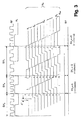
図3の第1の線は、復調器の入力部E1で受信された、かつ可変周波数Fを有する無線周波数信号RFを表す。第2の線は、カウンタ/分割器DIVの出力部における、したがって前に復調器のコアと呼ばれたものの入力部E2における信号Hsを表す。信号Hsは、周波数F/Nsである周波数を有する。S1〜SNdの符号を付けられた、図3の次のNd線は、遅延線DELによって遅延された周波数F/Nsの、かつこの遅延線のNd出力部S1〜SNdに存在するNd信号を表す。 The first line in FIG. 3 represents the radio frequency signal RF received at the demodulator input E1 and having a variable frequency F. The second line represents a counter / divider at the output of the DIV, so that the signal H s at the input E2 of those referred to as the core of the demodulator before. The signal H s has a frequency that is a frequency F / N s . Attached the sign of S 1 to S Nd, following N d line of FIG. 3, the frequency F / N s is delayed by the delay line DEL, and the delay line N d output section S 1 to S Nd Represents the Nd signal present in.
出力Ndの数が大きければ大きいほど(および2つの連続出力間の遅延増分ΔTが小さければ小さいほど)、復調器はそれだけ正確である。 Output N greater the number of d (and as the two delay increments ΔT between successive output smaller the), the demodulator is much accurate.
遅延線の出力の1つSmは、それが位相ロックループ用の基準として働くので、特定の役割を有する。出力Smは、入力周波数がF0である場合に、信号Hsの周期全体の遅延を確立する出力であるのが好ましい。これは、周波数変調信号の平均周波数に対して定義される基本遅延に基づいて位相ロックループを整列させるための最も単純な解決法である。遅延線の連続出力部間における基本遅延増分ΔTは、長い時定数を備えた位相ロックループゆえに固定されると考えることができる。 One of the delay line outputs, S m, has a specific role because it serves as a reference for the phase locked loop. The output S m is preferably an output that establishes a delay of the entire period of the signal H s when the input frequency is F 0 . This is the simplest solution for aligning the phase locked loop based on the fundamental delay defined for the average frequency of the frequency modulated signal. The basic delay increment ΔT between successive outputs of the delay line can be considered fixed due to the phase locked loop with a long time constant.
出力部Smからの遅延信号は、信号Hsが周波数F0/Nsである場合に、したがってSY0が送信されている間に、信号Hsの立ち上がりエッジと一致する立ち上がりエッジを有することが、図3から分かる。位相比較器CMPHの構造をそれ相応に修正することによって、信号Hsの立ち下がりエッジと一致する、出力部Smからの信号の立ち上がりエッジを想定することもまた可能であろう。 Delayed signal from the output section S m, when the signal H s is the frequency F 0 / N s, thus while the SY 0 is being transmitted, having a rising edge coincident with the rising edge of the signal H s Can be seen from FIG. By modifying the structure of the phase comparator CMPH accordingly, it would also be possible to assume a rising edge of the signal from the output S m that coincides with the falling edge of the signal H s .
シンボルSY0の終わりに、信号Hsの立ち上がりエッジにおいて、出力部Smに先行する出力部S1〜Sm−1の論理状態が、第1の論理状態(ここでは:ハイレベル1)にあるのに対して、出力部Sm〜SNdは、第2の論理状態(ここでは:ローレベル0)にある。順番に取った全ての出力部の状態は、11111000000である。
At the end of the symbol SY 0, at the rising edge of the signal H s, the logic state of the
次のシンボルSYaは、より高い周波数に対応する。シンボルSYaの終わりに、信号Hsの立ち上がりエッジにおいて、出力部Saの前における、遅延線の第1の出力部の状態は、レベル1であり、(出力部SNdは別として)Saから最後の出力部の状態は、レベル0である。順番に取った全ての出力の状態は、この例では110000000(1)である。最後の1は、目的を有しない。
The next symbol SY a corresponds to a higher frequency. At the end of the symbol SY a, at the rising edge of the signal H s, at the front of the output section S a, state of the first output portion of the delay line is a
最後に、シンボルSYbは、F0より低い周波数に対応し、シンボルSYbの終わりにおいて信号Hsの立ち上がりエッジの瞬間における遅延線の出力の状態は、111111111110である。すなわち、出力Sbの前は1であり、出力Sb〜出力SNdは0である。 Finally, symbol SY b corresponds to a frequency lower than F 0 and the state of the output of the delay line at the instant of the rising edge of signal H s at the end of symbol SY b is 111111111110. That is, the previous output S b is 1, the output S b ~ output S Nd is zero.
したがって、増加する遅延の方向における1状態から0状態への遷移の位置は、シンボルの長さの間の偏差を直接表し、符号11111000000は、シンボルSY0、すなわち平均周波数F0を表し、符号11000000xxは、シンボルSYa(より低い周波数)を表し、符号11111111110は、シンボルSYb(より高い周波数)を表す。 Therefore, the position of the transition from the 1 state to the 0 state in the direction of increasing delay directly represents the deviation between the lengths of the symbols, the code 11111000000 represents the symbol SY 0 , ie the average frequency F 0 and the code 11000000xx Represents the symbol SY a (lower frequency), and the code 11111111110 represents the symbol SY b (higher frequency).
したがって、出力の全体的状態は、温度計符号、すなわち一連の1状態から一連の0状態への遷移の位置によって値が定義される符号に従って、シンボルを定義する。 Thus, the overall state of the output defines a symbol according to a thermometer code, ie a code whose value is defined by the position of a transition from a series of 1 states to a series of 0 states.
Ndラッチ(D)のレジスタDFFは、(信号Hsの立ち上がりエッジによって定義された)シンボルの終わりの瞬間におけるこの符号を記憶し、コーダCODは、符号を(例えば)純粋な2値に変換して、ちょうど復調されたシンボル値を出力SYにおいて供給する。 N d register DFF latch (D) stores the code at the moment of the end of the (defined by the rising edge of the signal H s) symbols, coder COD, a conversion code (for example) to a pure binary The just demodulated symbol value is then supplied at the output SY.
表示の例において、シンボルの値は、シンボル期間が値ΔTだけ増分または減分されるたびに1単位だけ増分または減分されると仮定され、シンボルSY0は値0を有し、シンボルSYaは値−3を有し、シンボルSYbは値+5を有する。可能なシンボルの連続におけるシンボル値増分が、遅延増分2ΔTに対応するように変調が行われる場合に、コーダCODは、これを考慮して、温度計符号からシンボル値を決定しなければならないことが理解されよう。
In the example shown, the value of the symbol is assumed to be incremented or decremented by one unit each time the symbol period is incremented or decremented by the value ΔT, symbol SY 0 has the
復調器が最良の状態で機能するために、分割器DIV(それが存在する場合に)が、シンボルの開始に正確に同期されることが望ましい。次に、分割器DIVには、同期化入力部(図示せず)が含まれる。同期は、真の情報送信の開始前に、初期化符号の繰り返し送信に基づいて求めることができる。この点には後で戻る。 In order for the demodulator to function at its best, it is desirable that the divider DIV (if it exists) be accurately synchronized to the start of the symbol. Next, the divider DIV includes a synchronization input unit (not shown). Synchronization can be determined based on repeated transmission of initialization codes before the start of true information transmission. We will return to this point later.
図4は、無線周波数信号が位相変調される場合における、本発明による復調器の動作の例を表す。次に、シンボル期間が、無線周波数信号のNs周期であると見なされる。Ns周期の全期間は、シンボルの終わりが、位相変調されていないクロック周波数に対して、決定された位相だけ位相シフトされるようになる。例えば、第1の周期が期間T=(1+Φ/2π)/F0を有し、ここでF0が、無線信号の搬送波周波数であり、Φが、この信号を変調するために用いられる位相であると見なすことが可能である。Φは、シンボルSY0用にはゼロ(例えば)に等しく、かつシンボルSYaおよびSYb用にはΦaまたはΦbに等しい。続く周期は、期間1/F0を有する。図示の例において、Φaは負であり(他より短い、シンボルの第1の周期に帰着する)、Φbは正である(より長い第1の周期に帰着する)。図4に表されているのは、位相変調のこの例である。
FIG. 4 represents an example of the operation of the demodulator according to the invention when the radio frequency signal is phase modulated. A symbol period is considered to be the N s periods of the radio frequency signals. The entire period of N s period, the end of the symbol, with respect to the clock frequency which is not phase modulated, only determined phase will be phase-shifted. For example, the first period has a period T = (1 + Φ / 2π) / F 0 , where F 0 is the carrier frequency of the radio signal and Φ is the phase used to modulate this signal. It can be considered to be. Φ is equal to zero (for example) for symbol SY 0 and equal to Φ a or Φ b for symbols SY a and SY b . The following period has a
信号Hsは、シンボルの開始およびシンボルの終わりにおいて無線信号の立ち上がりエッジと同期する立ち上がりエッジを有する。 The signal H s has a rising edge that is synchronized with the rising edge of the radio signal at the beginning and end of the symbol.
シンボルの開始におけるHsの立ち上がりエッジ、およびシンボルの終わりにおける立ち上がりエッジを分離する期間が、シンボルの終わりを定義する立ち上がりエッジの瞬間における遅延線のNd遅延出力の状態によってもう一度測定される。出力Smは、位相変調Φがゼロである場合に、周期全体によって遅延される信号を供給する出力である。 The rising edge of H s at the beginning of the symbol, and the period separating the rising edge at the end of the symbol, is once again measured by the state of the N d delayed output of the delay line at the moment of the rising edge that defines the end of a symbol. The output S m is an output that provides a signal delayed by the entire period when the phase modulation Φ is zero.
ラッチレジスタの出力の状態はまた、信号Hsの周期の期間を表す温度計符号、およびしたがってシンボルの値を定義する。なぜなら、この期間が位相に直接リンクされるからである。 The state of the output of the latch register also defines the thermometer sign, and thus the value of the symbol, which represents the period of the signal H s period. This is because this period is directly linked to the phase.
位相変調が、非変調搬送波によって定義される絶対時間基準に対して位相シフトを確立することに存することが注目される。復調器が、先行するシンボルの終わりに対してNs周期の期間を測定するので、出力部で得られる温度計符号は、実際の変調シンボルではなく先行するシンボルに対するシンボル変動を表す。したがって、位相を変調するために用いられた真のシンボルは、検出された変動を、先行するシンボルの値に加えることによって得られる。加算レジスタ(図示せず)が、この目的のために、復調器の出力部に追加される。次に、安全のために、誤り訂正機構が、シンボル上のどんな復調誤差も全ての後続するシンボルに伝播するのを回避するために採用される。 It is noted that phase modulation resides in establishing a phase shift with respect to an absolute time reference defined by an unmodulated carrier. Since demodulator measures the preceding period of N s periods with respect to the end of the symbol, the thermometer code obtained at the output represents the symbol variation for the symbol that precede rather than actual modulation symbols. Thus, the true symbol used to modulate the phase is obtained by adding the detected variation to the value of the preceding symbol. A summing register (not shown) is added to the output of the demodulator for this purpose. Then, for safety, an error correction mechanism is employed to avoid propagating any demodulation error on the symbol to all subsequent symbols.
図2および図3は、周波数変調および位相変調の場合を示すが、この場合に、シンボルの送信期間は、正確に、シンボルの瞬間において無線周波数における信号のNs周期全体であり、第1の周期の期間は、位相変調の場合には、位相の値を考慮する。これらの2つの場合に、変調は、シンボルの開始およびシンボルの終わりの瞬間が無線周波数に対して整列されるので、いわゆる同期変調である。したがって、シンボル期間は、シンボルからシンボルへと可変であった。 2 and 3 show the case of frequency modulation and phase modulation, where the transmission period of the symbol is exactly the entire N s period of the signal at radio frequency at the instant of the symbol, In the case of phase modulation, the period value takes the phase value into consideration. In these two cases, the modulation is a so-called synchronous modulation, since the symbol start and end moments of the symbol are aligned with the radio frequency. Therefore, the symbol period was variable from symbol to symbol.
しかしながら、復調器はまた、受信信号が、固定シンボル期間を伴って非同期で変調される場合に動作することができる。これは、信号が位相変調される場合に特に真である。しかしながら、それはまた、無線周波数における信号の変調速度が比較的低いならば、周波数変調においても真になり得る。 However, the demodulator can also operate when the received signal is modulated asynchronously with a fixed symbol period. This is especially true when the signal is phase modulated. However, it can also be true in frequency modulation if the modulation rate of the signal at radio frequencies is relatively low.
図5は、後者の場合における復調を示す。シンボル期間は、周波数が、修正され、かつこのシンボル用に定義された値を取る間の期間である。しかしながら、遅延測定は、周波数Hsによって、すなわちNs/Fにリンクされた期間によって定義されるままであり、かつ逆に周波数およびしたがってシンボルの値に作用するために測定されなければならないのは実際にはこの期間である。 FIG. 5 shows the demodulation in the latter case. A symbol period is a period during which the frequency is modified and takes a value defined for this symbol. However, the delay measurement remains defined by the frequency H s , ie by the period linked to N s / F, and conversely it must be measured to affect the frequency and thus the value of the symbol. Actually this is the period.
この理由で、遅延線の出力の状態をラッチに記録するのは常にHs(=Ns/F)の立ち上がりエッジ(または常に立ち下がりエッジ)である。したがって、一定の期間のシンボルによる非同期変調の場合には、シンボルの終わりと、ラッチがトグルする瞬間との間に時間オフセットが存在する。 For this reason, it is always the rising edge (or always falling edge) of H s (= N s / F) that records the output state of the delay line in the latch. Thus, in the case of asynchronous modulation with symbols of a certain period, there is a time offset between the end of the symbol and the moment when the latch toggles.
シンボル期間は、平均周波数F0におけるNs周期に等しく取られるのが好ましい。したがって、シンボルSY0は、Ns/F0と正確に等しい期間を有する。しかしシンボルSYaおよびSYbは、同じ期間を有するが、それらの1つはNs/Faより少し長く、もう一方はNs/Fbより少し短い。しかしながら、周波数変動が低く、均一に分配されている場合に、そこから(シンボルの終わりの瞬間に対して)結果としてもたらされる測定瞬間誤差は、遅延線における基本遅延ΔTの期間より小さくすることが可能であり、この場合にはシンボル決定誤差は存在しない。 The symbol period is preferably taken equal to the N s period at the average frequency F 0 . Thus, the symbol SY 0 has a period that is exactly equal to N s / F 0 . However, symbols SY a and SY b have the same period, but one of them is slightly longer than N s / F a and the other is slightly shorter than N s / F b . However, when the frequency variation is low and evenly distributed, the resulting measurement instantaneous error (relative to the instant of the end of the symbol) can be smaller than the duration of the basic delay ΔT in the delay line. In this case, there is no symbol determination error.
一定の期間のシンボルを用いる非同期変調の場合における誤差のリスクが、Nsがより大きくなると(および周波数変調の場合には、変調指数がより低くなると)、それだけ低くなることが注目される。 It is noted that the risk of error in the case of asynchronous modulation using symbols of a certain period becomes lower as N s becomes larger (and in the case of frequency modulation, the modulation index becomes lower).
同期または非同期であろうと、周波数または位相であろうと、変調のタイプにかかわらず、復調器は、(Ndが1より大きい場合に)Ndラッチのレジスタの出力部において、温度計符号、すなわち、復調されたシンボルの値が、連続する一連の論理0状態から、連続する一連の論理1状態への遷移の位置によって定義される温度計符号を供給する。この特定の特徴によって、必要に応じて復調誤差の検出を確認することが可能になる。一連の1状態から一連の0状態への遷移が検出されない場合、さもなければこのタイプの多数の遷移が検出された場合には、復調されたシンボルは、誤っていると見なされて拒否される。
Regardless of the type of modulation, whether synchronous or asynchronous, frequency or phase, the demodulator (if Nd is greater than 1) has a thermometer code, i.e., at the output of the register of the Nd latch. The demodulated symbol value provides a thermometer code defined by the position of the transition from a continuous series of
続く図は、図2の周波数分割器、遅延線、位相比較器、および復調器の積分器を実現できるようにする方法を示す実例としてのみ提示される。 The following figures are presented only as an illustration showing how to enable the frequency divider, delay line, phase comparator, and demodulator integrator of FIG. 2 to be implemented.
図6は、Ns=8の場合に周波数をNsで割るための例示的な周波数分割器を表す。これは、単に例であり、周波数分割器を作製するための多くの周知の解決法が存在する。 FIG. 6 represents an exemplary frequency divider for dividing the frequency by N s when N s = 8. This is only an example, and there are many well-known solutions for making frequency dividers.
分割器は、カウンタである。それには、3ビットカウンタを形成する3つのDラッチが含まれる。これら3つのラッチのクロック入力部は、例えば、RFIDタグのアンテナから得られる無線周波数RFの信号を受信する。各ラッチの入力部Dは、それぞれのマルチプレクサMUX1、MUX2、MUX3の出力を受信する。マルチプレクサは、同期位相中に決定値(0と7との間)を備えたカウンタの初期化を保証するために用いられ、次に、それらは、ラッチ出力部と入力部との間の必要なループバックを保証する。これらのループバックは、必要な周波数分割を確立する。したがって、第1のラッチは、その入力Dがその出力から始まるので、RF周波数を2で割る。第2のラッチは、その入力部が、第1のラッチによって制御されたORゲートを通して、その出力を受信するので、周波数を4で割る。第3のラッチは、その入力部が、他の2つのラッチによって制御された排他的ORゲートを通して、その出力を受信するので、周波数を8で割る。 The divider is a counter. It includes three D latches that form a 3-bit counter. The clock inputs of these three latches receive a radio frequency RF signal obtained from, for example, an RFID tag antenna. The input D of each latch receives the outputs of the respective multiplexers MUX1, MUX2, and MUX3. Multiplexers are used to ensure the initialization of the counter with the decision value (between 0 and 7) during the synchronization phase, and then they are required between the latch output and the input. Guarantees loopback. These loopbacks establish the necessary frequency division. Thus, the first latch divides the RF frequency by 2 because its input D begins at its output. The second latch divides the frequency by 4 because its input receives its output through an OR gate controlled by the first latch. The third latch divides the frequency by 8 because its input receives its output through an exclusive OR gate controlled by the other two latches.
同期化入力部および初期化バスが設けられる。同期化入力部「sync」は、マルチプレクサを制御して、同期化中に初期値(0〜7)に対応する論理状態をラッチに適用する。 A synchronization input and an initialization bus are provided. The synchronization input “sync” controls the multiplexer to apply a logic state corresponding to the initial value (0-7) to the latch during synchronization.
同期化は、いくつかの方法で、特にシンボルフレームのヘッドにおける同期化符号を送信することによってか、または特定の変調されたシンボルを送信することによってか、または同期化パルスの振幅変調によって実行することができる。 Synchronization is performed in several ways, in particular by transmitting a synchronization code at the head of the symbol frame, by transmitting a specific modulated symbol, or by amplitude modulation of the synchronization pulse be able to.
フレームの開始における符号による同期化の場合には、少なくともNs回繰り返される長さNc(シンボルNcの数)の符号をヘッダが含むように準備がなされる。 In the case of synchronization with a code at the start of the frame, provision is made for the header to contain a code of length N c (number of symbols N c ) repeated at least N s times.
小さな状態機械(図示せず)が、RF周波数における信号のNc周期ごとに同期化パルスを、復調器においてNs回生成する。各パルスにおいて、3つのラッチによって形成されたカウンタに印加される初期値は、Nsの可能な初期値が生成されるまで、1単位ずつ増分される。初期化が毎回異なるので、復調器は、Ncの異なる符号を生成する。これらの符号の1つが、予想された初期化符号と同一であり、予想された符号の検出によって、カウンタ同期化プロセスが停止され、カウンタは、検出された同期状態から、引き続きNsによる分割を実行する。 A small state machine (not shown) generates a synchronization pulse N s times in the demodulator every N c periods of the signal at the RF frequency. In each pulse, the initial value applied to the counter formed by three latches until possible initial value of N s is produced, it is incremented by one unit. Since the initialization is different each time, the demodulator generates N c different codes. One of these codes is identical to the expected initialization code and detection of the expected code stops the counter synchronization process and the counter continues to divide by N s from the detected synchronization state. Execute.
代替として、同期化は、Ncシンボルの特定の符号を用いてではなく、データ送信では使用されない特定のシンボルを用いて行うことができる。この原理は、復調器が特定のシンボルを見つけるまで一連のNsの異なる初期化を用いる前のものと同じである。 Alternatively, the synchronization can be done with specific symbols that are not used in data transmission, rather than with a specific code of Nc symbols. This principle is the same as before using a series of N s different initializations until the demodulator finds a particular symbol.
最後に、送信機に同期化パルスを振幅において変調させることを想定することがまた可能であるが、しかしそのときは、復調器には、振幅復調手段を設けなければならない。 Finally, it is also possible to assume that the transmitter modulates the synchronization pulse in amplitude, but then the demodulator must be provided with amplitude demodulation means.
図7は、本発明による復調器で使用できる論理遅延線の構造の例を表す。それは、信号Hsを受信するための入力部E2と、信号Hsと同じ立ち上がりエッジを有するがしかしこの信号に対して遅延された論理信号を供給するNd出力部S1〜SNdと、を有する。中間出力部(前に言及した出力部Sm)が、信号Hsのエッジとエッジが一致する遅延信号を供給する。他の出力部は、増分ΔTだけ互いにオフセットされた遅延信号を供給する。線には、反転セルのペアによってそれぞれが形成される、Ndのカスケードされた同一ステージが含まれる。各ステージは、それが前のステージから受信する信号を、ΔTだけ遅延させながら、その入力部からその出力部へ伝播する。 FIG. 7 represents an example of the structure of a logic delay line that can be used in a demodulator according to the present invention. It includes an input unit E2 for receiving the signal H s, and the signal H s have the same rising edge as but provides a logic signal which is delayed relative to the signal N d output section S 1 to S Nd, Have An intermediate output section (output section S m referred to above ) provides a delayed signal whose edge coincides with the edge of signal H s . The other outputs provide delayed signals that are offset from each other by an increment ΔT. The line, respectively, by inverting the cell pairs are formed, it includes cascaded identical stages of N d. Each stage propagates the signal it receives from the previous stage from its input to its output, delaying by ΔT.
セルは、ドレインを共通にし、かつゲートを共通にしたPMOSトランジスタQ1および直列NMOSトランジスタQ2と、ペアQ1、Q2と直列のNMOS供給トランジスタQ3であって、遅延線の制御入力部Ec上に存在するDC電圧Vcrtrlによりゲートを制御されるトランジスタQ3と、によって形成される。別のトランジスタペアQ’1、Q’2が、ペアQ1、Q2のように実装され、供給トランジスタQ’3が、Q3のように実装される。ペアQ1、Q2は、第1のインバータとして働き、ペアQ’1、Q’2は、第2のインバータとして働き、この第2のインバータの出力部は、遅延線の次のステージの入力部にリンクされる。出力インバータI1は、その入力部が、Q’1およびQ’2の共通ドレインに接続され、その出力部は、Nd出力部からの遅延線のそれぞれの出力部を構成する。 Cell, and the common drain, and a PMOS transistor Q1 and the series NMOS transistors Q2 and the gate in common, a pair Q1, Q2 in series with NMOS source transistors Q3, present on the control input E c of the delay line And a transistor Q3 whose gate is controlled by a DC voltage V crtrl . Another transistor pair Q′1, Q′2 is implemented as pair Q1, Q2 and supply transistor Q′3 is implemented as Q3. The pair Q1, Q2 serves as a first inverter, the pair Q′1, Q′2 serves as a second inverter, and the output part of the second inverter is connected to the input part of the next stage of the delay line. Linked. Output inverter I1 has its input is connected to the common drain of the Q'1 and Q'2, whose output constitutes a respective output of the delay line from the N d output unit.
線の2つの出力間の遅延増分ΔTは、第1のインバータ(Q1、Q2)および第2のインバータQ’1、Q’2のトグル遅延の和である。 The delay increment ΔT between the two outputs of the line is the sum of the toggle delays of the first inverter (Q1, Q2) and the second inverter Q'1, Q'2.
遅延増分ΔTは、トランジスタQ3およびQ’3の制御電圧Vctrlを変えることによって調整される。この電圧は、位相ロックループから(実際には、積分コンデンサCintから)生じ(図2を基準)、これによって、遅延増分の自動調整が保証される。Vctrlが高ければ高いほど、Q1、Q2またはQ’1、Q’2などのトランジスタペアの出力部における容量性ノードの放電電流がそれだけ高く、これらのペアのドレインからなる容量性ノードの放電がそれだけ速くなる。(同じステージまたは次のステージにおける)次のトランジスタペアのトグルレベルは、より速く達成され、したがってステージによって生成される遅延はより小さい。反対に、Vctrlがより多く減少すればするほど、放電はそれだけ遅くなり、遅延はそれだけ増加する。 Delay increment ΔT is adjusted by varying the control voltage V ctrl of the transistors Q3 and Q'3. This voltage arises from the phase-locked loop (actually from the integrating capacitor C int ) (referenced to FIG. 2), which ensures automatic adjustment of the delay increment. The higher V ctrl is, the higher the discharge current of the capacitive node at the output of the transistor pair such as Q1, Q2 or Q′1, Q′2, and the discharge of the capacitive node consisting of the drains of these pairs It gets faster. The toggle level of the next transistor pair (in the same or the next stage) is achieved faster and therefore the delay generated by the stage is smaller. Conversely, the more Vctrl decreases, the slower the discharge and the more the delay.
好ましくは、次のセルペアによってゲートが制御される帰還トランジスタ(Q4、Q’4)が、各供給トランジスタ(Q3、Q’3)と並列に設けられる(Q3と並列なトランジスタQ4である場合には同じステージの次のセルペア、またはQ’3と並列なトランジスタQ’4である場合には次のステージの次のセルペア)。このトランジスタは、次のセルがトグルした後で、セルペアの出力ノードを非常に速く放電させ、これは、この出力ノードがゼロに切り替わる場合に、より急勾配の遷移エッジを有することができるようにする。 Preferably, a feedback transistor (Q4, Q′4) whose gate is controlled by the next cell pair is provided in parallel with each supply transistor (Q3, Q′3) (in the case of a transistor Q4 in parallel with Q3) The next cell pair in the same stage, or the next cell pair in the next stage if it is a transistor Q′4 in parallel with Q′3). This transistor discharges the output node of the cell pair very quickly after the next cell toggles, so that it can have a steeper transition edge if this output node switches to zero. To do.
図8は、本発明による復調器において使用できる位相比較器の例を表す。それは、非同期論理モードで動作する論理ゲートセットからなる比較器である。それは、その出力部において、遅延線の出力Smおよび周波数分割器DIVから出力される信号Hsを受信して、これらの2つの出力の位相を比較するようにする。 FIG. 8 represents an example of a phase comparator that can be used in a demodulator according to the present invention. It is a comparator consisting of a set of logic gates operating in asynchronous logic mode. It receives at its output the delay line output S m and the signal H s output from the frequency divider DIV and compares the phase of these two outputs.
比較は、入力信号の立ち上がりエッジに基づいて行われる。比較器は、2つの出力部P+およびP−を有し、かつこれらの出力部において、比較器の2つの入力における立ち上がりエッジの相対的地位に開始および終わりが依存する正パルスを生成する。例えば、信号Hsの立ち上がりエッジが出力部Smからの信号のエッジに先行する場合に、P+上のパルスは、P−上のパルスより早く開始する。 The comparison is performed based on the rising edge of the input signal. The comparator has two outputs P + and P-, and at these outputs generates a positive pulse whose start and end depend on the relative position of the rising edge at the two inputs of the comparator. For example, if the rising edge of the signal H s precedes the signal edge from the output unit S m, P + upper pulse starts earlier than P- top pulse.
遅延線用に意図された制御電圧VctrlをコンデンサCint上で生成する積分器に供給するために用いられるのがこれらのパルスである。積分器は、この場合に、電荷ポンプからなり、観察された位相シフトに従って電圧Vctrlを増加または低減する正または負の電流パルスによって、コンデンサCintを充電または放電する。正パルスが負パルスより長い場合に、コンデンサは充電され、そうでなければコンデンサは放電される。入力信号が互いに同相である場合に、平衡が実現され、次に位相比較器は、両方とも等しい期間の短い正パルスおよび短い負パルスを周期的に供給し、これらのパルスは、補償され、かつコンデンサの端子における電圧をその平衡値で維持する。 That used to supply the control voltage V ctrl, which is intended for the delay line integrator that generated on the capacitor C int is these pulses. The integrator in this case consists of a charge pump and charges or discharges the capacitor C int with positive or negative current pulses that increase or decrease the voltage Vctrl according to the observed phase shift. If the positive pulse is longer than the negative pulse, the capacitor is charged, otherwise the capacitor is discharged. When the input signals are in phase with each other, a balance is achieved, and then the phase comparator periodically provides short positive and short negative pulses of equal duration, these pulses are compensated and Maintain the voltage at the capacitor terminals at its equilibrium value.
図9は、電荷ポンプの可能な実施形態を表すが、従来の電荷ポンプ方式がまた、この方式の代わりに用いることができる。 Although FIG. 9 represents a possible embodiment of a charge pump, a conventional charge pump scheme can also be used in place of this scheme.
位相比較器からのパルスP+およびP−が、電荷ポンプの2つの入力部に印加され、電荷ポンプは、それぞれP+およびP−におけるパルス幅の関数である正および負の電流を生成し、電流の1つが、積分コンデンサCintを充電し、もう一方が、このコンデンサを放電する。 Pulses P + and P- from the phase comparator are applied to the two inputs of the charge pump, which generates positive and negative currents that are functions of the pulse width at P + and P-, respectively, One charges the integrating capacitor C int and the other discharges this capacitor.
図10は、既に説明した遅延線の上流における補助遅延線を用いる、復調器の変形実施形態を表す。この変形は、ある場合に、および特に数Nsが、2もしくは4を超える場合に、またはたとえ可能なシンボルの数が大きい場合であっても、遅延線DELにおける出力の数を低減するのに有用である。その理由は、例えばNsが大きい場合に、出力Smにおける高い平均遅延(信号Hsの周期全体、したがってRF信号の周期期間のNs倍の遅延)、および同時に異なるシンボル期間を識別できる、異なる出力間の低い値の増分ΔTの両方を生成することが必要であるからである。この場合に、遅延線DELに対して既に遅延された信号を供給する補助遅延線DELauxを用いることが好ましい。したがって、補助遅延線は、主な遅延を確立し、遅延線DELは、復調に必要なNdの連続増分ΔTを、この主な遅延から確立する。主な遅延は、測定する必要がある最小期間に従って選択される。典型的には、変調が、周波数Ns/F0のまわりの周波数変調であり、Ns/Fmax〜Ns/Fminに及ぶ信号Hs周期に帰着する場合に、遅延線DELaux用にはNs/Fmaxに等しい主な遅延が選択される。 FIG. 10 represents a modified embodiment of the demodulator using an auxiliary delay line upstream of the delay line already described. This deformation, in some cases, and in particular the number N s is, if more than 2 or 4, or even when the number of even possible symbol large, to reduce the number of output of the delay line DEL Useful. The reason is that, for example, when N s is large, a high average delay in the output S m (the entire period of the signal H s and hence N s times the period of the RF signal) and at the same time different symbol periods can be identified This is because it is necessary to generate both low value increments ΔT between different outputs. In this case, it is preferable to use an auxiliary delay line DEL aux that supplies a signal already delayed to the delay line DEL. Therefore, the auxiliary delay line, to establish a primary delay, the delay line DEL is a continuous incremental ΔT of N d necessary for demodulation is established from the primary delay. The main delay is selected according to the minimum period that needs to be measured. Typically for the delay line DEL aux when the modulation is a frequency modulation around the frequency N s / F 0 , resulting in a signal H s period ranging from N s / F max to N s / F min A main delay equal to N s / F max is selected for.
したがって、補助遅延線DELauxは、主な遅延だけ遅延された信号Hsを供給する出力部Xaを有し、遅延線DELは、やはり、この主な遅延に対してΔTだけ増分される遅延を確立するNd出力部を有する。好ましくは、出力部Smは、図2の実施形態におけるように、平均変調周波数F0用の信号Hsの立ち上がりエッジと立ち上がりエッジが同相である信号を供給する。線DELauxもまた、この平均変調周波数F0にロックされるのが好ましいが、ロッキングは、線DEL用と同じ方法で行われる。この目的のために、好ましくは、線DELauxは、別の遅延された出力部Xb、すなわち、その立ち上がりエッジが、平均周波数F0用のHsの立ち上がりエッジとほぼ同期する出力部Xbを有する。線DELをロックするために出力部Smが用いられるのと同じ方法で、補助線DELauxの遅延をロックするために用いられるのはこの出力部Xbである。したがって、線DELauxのロックループには、信号Hsおよび出力Xbを受信する位相比較器CMPHauxと、位相比較器の出力を受信する電荷ポンプCHPauxと、変調シンボルの期間よりはるかに大きい時定数で電荷ポンプの出力を積分する積分コンデンサCint−auxと、が含まれる。 Thus, the auxiliary delay line DEL aux has an output X a that provides a signal H s delayed by a main delay, and the delay line DEL is also a delay that is incremented by ΔT relative to this main delay. Has an Nd output. Preferably, the output unit S m supplies a signal in which the rising edge and the rising edge of the signal H s for the average modulation frequency F 0 are in phase as in the embodiment of FIG. The line DEL aux is also preferably locked to this average modulation frequency F 0 , but the locking is done in the same way as for the line DEL. For this purpose, preferably, the line DEL aux is another delayed output unit X b, i.e., the rising edge, the output unit X b which is substantially synchronized with the rising edge of H s for the average frequency F 0 Have In the same way as the output section S m is used to lock the line DEL, that used to lock the delay of the auxiliary line DEL aux is the output unit X b. Thus, the locked loop of line DEL aux has a phase comparator CMPH aux that receives signal H s and output X b , a charge pump CHP aux that receives the output of the phase comparator, and much larger than the duration of the modulation symbol And an integrating capacitor C int-aux that integrates the output of the charge pump with a time constant.
図10の方式を用いると、Ns/F0−Nd.ΔT/2に等しい遅延値が、線DELauxによって確立された主な遅延として取られた場合に、遅延線DELは、この主な遅延から、値ΔTのNd連続遅延を確立し、その結果、線DELによって確立される遅延セットは、遅延Ns/F0−Nd.ΔT/2から遅延Ns/F0+Nd.ΔT/2まで及び、分解能ΔTで、この間隔に対応する期間におけるシンボルの測定を可能にする。 When the method of FIG. 10 is used, N s / F 0 −N d . If a delay value equal to ΔT / 2 is taken as the main delay established by the line DEL aux , the delay line DEL establishes an N d continuous delay of value ΔT from this main delay, and consequently , The delay set established by line DEL is the delay N s / F 0 −N d . ΔT / 2 to delay N s / F 0 + N d . With a resolution of ΔT up to ΔT / 2, it is possible to measure symbols in a period corresponding to this interval.
遅延線DELauxは、線DELのような多数のステージを有する必要はないが、しかしそのステージは、ΔTより大きい遅延を確立する。 Delay line DEL aux need not have multiple stages like line DEL, but that stage establishes a delay greater than ΔT.
図11は、Ndが1に等しい実施形態を表す。この実施形態によって、わずか2つの可能な状態だけを有する一連のシンボルを復調することが可能になるが、しかしそれは、非常に大きな単純性、および集積回路チップにおける非常に低い体積という利点を有する。それは、周波数変調または位相変調モードにおいて、先行する実施形態のように動作する。周波数変調モードにおいて、復調される2つのシンボルに対応する無線周波数信号RFの周波数は、Ns/F1=T0+ΔTおよびNs/F2=T0−ΔTであるように、それぞれF1およびF2であり、平均周波数は、F0=Ns/T0である。Nd=1では、どんなシンボルも平均周波数F0によって表すことが不可能であることが注目される。位相変調モードにおいて、復調されるシンボルはまた、期間T0+ΔTおよびT0−ΔTに対応するが、これらの異なる期間は、シンボル間の遷移の瞬間における無線周波数(周波数F0)の信号の位相跳躍に起因する。例えばπ/2の位相跳躍では、ΔTは、T0/4Ns(無線周波数における信号の1/4周期)に等しい。Ns=1の場合に、πの位相跳躍が不可能であることが注目される。 FIG. 11 represents an embodiment in which N d is equal to 1. This embodiment makes it possible to demodulate a series of symbols having only two possible states, but it has the advantage of a very large simplicity and a very low volume in an integrated circuit chip. It operates like the previous embodiment in frequency modulation or phase modulation mode. In the frequency modulation mode, the frequency of the radio frequency signal RF that corresponds to two symbols to be demodulated, as is N s / F 1 = T 0 + ΔT and N s / F 2 = T 0 -ΔT, respectively F 1 And F 2 and the average frequency is F 0 = N s / T 0 . Note that with N d = 1, no symbol can be represented by the average frequency F 0 . In the phase modulation mode, the demodulated symbols also correspond to the periods T 0 + ΔT and T 0 −ΔT, but these different periods are the phase of the signal of the radio frequency (frequency F 0 ) at the moment of transition between the symbols. Due to the leap. For example, for a phase jump of π / 2, ΔT is equal to T 0 / 4N s (1/4 period of the signal at radio frequency). It is noted that π phase jump is not possible when N s = 1.
復調器には、前に説明したように、Nsが1を超える場合にのみ、すなわち、シンボル期間が、無線周波数信号RFのいくつかの(Ns)周期(または平均周期)である場合に、入力信号の周波数を整数Nsで割る周波数分割器が含まれる。 The demodulator, as explained above, only when N s exceeds 1, ie when the symbol period is several (N s ) periods (or average periods) of the radio frequency signal RF. A frequency divider is included that divides the frequency of the input signal by the integer N s .
分割器DIVの後の復調器のコアには、単一の出力部Smだけを有する(または単一の出力部だけが用いられる)遅延線が含まれ、かつこのコアにはまた、単一のラッチD、すなわち、その入力部Dが、遅延線の出力Smを受信し、かつそのクロック入力部CLKが、周波数F/Nsの入力信号Hsを受信する単一のラッチDが含まれる。信号Hsの立ち上がりエッジ(例えば)に基づいて、ラッチは、その入力部Dに課された状態を取る。この状態は、出力部Smにおいて遅延された第1の立ち上がりエッジの後で、Hsの第2の立ち上がりエッジがクロック入力部CLKに到着する瞬間に依存する。 The core of the demodulator after the divider DIV includes a delay line having only a single output S m (or only a single output is used), and this core also includes a single output Latch D, that is, its input D receives a delay line output S m and its clock input CLK receives a single latch D receiving an input signal H s of frequency F / N s It is. Based on the rising edge of the signal H s (for example), the latch takes the state imposed on its input D. This state, after the first rising edge which is delayed at the output S m, depending on the moment when the second rising edge of H s arrives at the clock input CLK.
出力部Smにおける遅延は、信号Hsの平均周期T0によるのが好ましい。それは、信号Hsの立ち下がりエッジが、ラッチのクロック入力CLKを制御するために用いられる場合には、半周期であってもよい。 Delay at the output S m is that the average period T 0 of the signal H s preferred. It may be a half cycle if the falling edge of the signal H s is used to control the clock input CLK of the latch.
T0(またはT0/2)だけ遅延される期間T0+ΔTのシンボルに関して、ラッチの状態は、このシンボルを表す第1の2進値を取る。期間T0−ΔTのシンボルに関し、ラッチの状態は、このシンボルを表す反転2進値を取る。 For a symbol of period T 0 + ΔT delayed by T 0 (or T 0/2 ), the state of the latch takes a first binary value representing this symbol. For a symbol of period T 0 -ΔT, the state of the latch takes an inverted binary value representing this symbol.
回路が、できるだけ単純化されることになる場合に、予想される平均周期または半周期T0またはT0/2に等しい遅延を供給する固定遅延線が用いられる。さもなければ、かなり長い時定数にわたって、期間T0−ΔTのシンボルと同数の、期間T0+ΔTのシンボルが受信されると仮定することによって、ロックされる遅延が、受信信号の平均周波数にロックされる前述の実施形態におけるのと同じ方法を用いることができる。この場合には、図11において点線で表され、かつ前に説明したのと同一の位相ロックループが用いられる。それは、一側で入力信号Hsを、かつ他側で出力部Smにおける信号を受信する。 If the circuit is to be simplified as much as possible, a fixed delay line is used that provides a delay equal to the expected average period or half period T 0 or T 0/2 . Otherwise, over a fairly long time constant, the locked delay is locked to the average frequency of the received signal by assuming that the same number of symbols of period T 0 + ΔT are received as the number of symbols of period T 0 -ΔT. The same method as in the previous embodiment can be used. In this case, the same phase-locked loop represented by the dotted line in FIG. 11 and described above is used. It the input signal H s at one side, and receives the signal at the output S m at the other side.
単一の遅延線および単一のラッチだけがあるとすると、2つのシンボルを表す2つの周波数F1およびF2間の差が、信号Hsの立ち上がりまたは立ち下がりエッジ用に十分なように復調されることが好ましく、これによって、T0だけ遅延された信号の立ち上がりまたは立ち下がりエッジに近すぎないようにラッチの入力CLKが制御され、さもなければ誤差が発生する可能性がある。2つのシンボルに対応する周期が、それぞれT0+ΔTおよびT0−ΔTであるような値であって、ΔTが、T0の15%〜35%であるような値が理想的である。次に、変調において用いられる2つの無線周波数間の比率F2/F1は、約1.3〜2である。遅延線は、図7の方式から作製することができ、この場合には、遅延T0またはT0/2に対応する単一の出力部だけが用いられる。 Given only a single delay line and a single latch, the difference between the two frequencies F 1 and F 2 representing the two symbols is demodulated so that it is sufficient for the rising or falling edge of the signal H s Preferably, this controls the input CLK of the latch so that it is not too close to the rising or falling edge of the signal delayed by T0, otherwise errors may occur. Ideally, the periods corresponding to the two symbols are values such that T 0 + ΔT and T 0 −ΔT, respectively, and ΔT is 15% to 35% of T 0 . Next, the ratio F 2 / F 1 between the two radio frequencies used in the modulation is about 1.3-2. The delay line can be made from the scheme of FIG. 7, in which case only a single output corresponding to the delay T 0 or T 0/2 is used.
Claims (13)
− 一方では前記入力信号を、他方では前記遅延線の前記出力の1つを受信する位相比較器(CMPH)と
− 前記シンボルの期間よりはるかに大きい時定数を備え、前記位相比較器の出力を受信し、かつ遅延線ロック信号を生成し、前記入力周波数の平均値に従ってこの線の遅延をロックする積分器(PCH、Cint)と、
を含むことを特徴とする、請求項1に記載の復調器。 The delay line is a line with a delay controlled by a locked loop, and the locked loop is
A phase comparator (CMPH) that receives the input signal on the one hand and one of the outputs of the delay line on the other side, and has a time constant much larger than the period of the symbol, and outputs the output of the phase comparator An integrator (PCH, C int ) that receives and generates a delay line lock signal and locks the delay of this line according to the average value of the input frequencies;
The demodulator according to claim 1, comprising:
− 一方では前記入力信号を、他方では前記補助遅延線の出力を受信する第2の位相比較器と
− 前記シンボルの期間よりはるかに大きい時定数を備え、前記第2の位相比較器の出力を受信し、かつ前記補助遅延線用のロック信号を生成して、前記入力周波数の平均値に従ってこの線の遅延をロックするようにする積分器と、
を含むことを特徴とする、請求項5に記載の復調器。 The auxiliary delay line is controlled by a second lock loop, and the second lock loop is
A second phase comparator that receives the input signal on the one hand and the output of the auxiliary delay line on the other side, and a time constant that is much larger than the period of the symbol, the output of the second phase comparator being An integrator for receiving and generating a lock signal for the auxiliary delay line to lock the delay of the line according to an average value of the input frequency;
The demodulator according to claim 5, comprising:
Applications Claiming Priority (3)
| Application Number | Priority Date | Filing Date | Title |
|---|---|---|---|
| FR0902226A FR2945398B1 (en) | 2009-05-07 | 2009-05-07 | DEMODULATOR AND SYSTEM FOR TRANSMITTING MODULATED INFORMATION, IN PARTICULAR FOR RADIOFREQUENCY IDENTIFICATION LABEL |
| FR0902226 | 2009-05-07 | ||
| PCT/EP2010/056004 WO2010128030A1 (en) | 2009-05-07 | 2010-05-04 | Demodulator and system for transmitting modulated information, in particular for radiofrequency identification tags |
Publications (1)
| Publication Number | Publication Date |
|---|---|
| JP2012526437A true JP2012526437A (en) | 2012-10-25 |
Family
ID=41404517
Family Applications (1)
| Application Number | Title | Priority Date | Filing Date |
|---|---|---|---|
| JP2012509006A Ceased JP2012526437A (en) | 2009-05-07 | 2010-05-04 | Demodulator and system for transmitting modulated information, especially for radio frequency identification tags |
Country Status (5)
| Country | Link |
|---|---|
| US (1) | US8988144B2 (en) |
| EP (1) | EP2428011B1 (en) |
| JP (1) | JP2012526437A (en) |
| FR (1) | FR2945398B1 (en) |
| WO (1) | WO2010128030A1 (en) |
Families Citing this family (5)
| Publication number | Priority date | Publication date | Assignee | Title |
|---|---|---|---|---|
| US8290463B2 (en) * | 2009-09-14 | 2012-10-16 | ConvenientPower HK Ltd. | Universal demodulation and modulation for data communication in wireless power transfer |
| CN103366213B (en) * | 2012-03-31 | 2016-08-03 | 华矽半导体股份有限公司 | Active Electronic Tag and Its Signal Modulation Method |
| JP6414513B2 (en) * | 2015-06-05 | 2018-10-31 | アイシン・エィ・ダブリュ株式会社 | Rotating electrical machine control device |
| RU180812U1 (en) * | 2018-02-06 | 2018-06-22 | Федеральное государственное бюджетное образовательное учреждение высшего образования "МИРЭА - Российский технологический университет" | INTERSEQUENT REGENERATOR OF QUASI-STATIONARY SEQUENCE OF SUBNANOSECOND RADIO PULSES |
| RU205216U1 (en) * | 2021-02-16 | 2021-07-05 | Константин Анатольевич Бойков | ULTRA FAST PULSE REGENERATOR WITH DETECTION FUNCTION |
Citations (3)
| Publication number | Priority date | Publication date | Assignee | Title |
|---|---|---|---|---|
| JPH0276348A (en) * | 1988-09-12 | 1990-03-15 | Fujitsu Ten Ltd | Digital delay detector |
| JPH0548663A (en) * | 1990-07-20 | 1993-02-26 | Nec Corp | Phase demodulator |
| US5990733A (en) * | 1997-02-19 | 1999-11-23 | Intermec Ip Corp. | Delay line ramp demodulator |
Family Cites Families (7)
| Publication number | Priority date | Publication date | Assignee | Title |
|---|---|---|---|---|
| US4309673A (en) * | 1980-03-10 | 1982-01-05 | Control Data Corporation | Delay lock loop modulator and demodulator |
| EP0467712B1 (en) | 1990-07-20 | 1998-04-29 | Nec Corporation | Phase demodulator for psk-modulated signals |
| KR100431716B1 (en) * | 2001-09-29 | 2004-05-17 | 주식회사 버카나와이어리스코리아 | FSK Demodulator using DLL and a demodulating method |
| US7154978B2 (en) * | 2001-11-02 | 2006-12-26 | Motorola, Inc. | Cascaded delay locked loop circuit |
| KR101030768B1 (en) * | 2004-08-26 | 2011-04-27 | 삼성전자주식회사 | Low power and high frequency wide-range delay locked loop circuit and optical driver system including the same |
| FR2917557A1 (en) * | 2007-06-15 | 2008-12-19 | Commissariat Energie Atomique | DEVICE FOR DEMODULATING A SIGNAL COMPRISING INFORMATION TRANSLATING BY MODULATION OF THE PHASE OF A CARRIER |
| US8044742B2 (en) * | 2009-03-11 | 2011-10-25 | Qualcomm Incorporated | Wideband phase modulator |
-
2009
- 2009-05-07 FR FR0902226A patent/FR2945398B1/en not_active Expired - Fee Related
-
2010
- 2010-05-04 US US13/266,826 patent/US8988144B2/en active Active
- 2010-05-04 WO PCT/EP2010/056004 patent/WO2010128030A1/en active Application Filing
- 2010-05-04 EP EP10715889A patent/EP2428011B1/en active Active
- 2010-05-04 JP JP2012509006A patent/JP2012526437A/en not_active Ceased
Patent Citations (3)
| Publication number | Priority date | Publication date | Assignee | Title |
|---|---|---|---|---|
| JPH0276348A (en) * | 1988-09-12 | 1990-03-15 | Fujitsu Ten Ltd | Digital delay detector |
| JPH0548663A (en) * | 1990-07-20 | 1993-02-26 | Nec Corp | Phase demodulator |
| US5990733A (en) * | 1997-02-19 | 1999-11-23 | Intermec Ip Corp. | Delay line ramp demodulator |
Also Published As
| Publication number | Publication date |
|---|---|
| US20120044017A1 (en) | 2012-02-23 |
| EP2428011B1 (en) | 2013-03-27 |
| FR2945398A1 (en) | 2010-11-12 |
| EP2428011A1 (en) | 2012-03-14 |
| US8988144B2 (en) | 2015-03-24 |
| FR2945398B1 (en) | 2011-06-10 |
| WO2010128030A1 (en) | 2010-11-11 |
Similar Documents
| Publication | Publication Date | Title |
|---|---|---|
| US7826583B2 (en) | Clock data recovery apparatus | |
| EP2781025B1 (en) | Apparatus and method for recovering burst-mode pulse width modulation (pwm) and non-return-to-zero (nrz) data | |
| KR940001724B1 (en) | Phase synchronization circuit | |
| US6674772B1 (en) | Data communications circuit with multi-stage multiplexing | |
| US10097187B2 (en) | Digital synthesizer, radar device and method therefor | |
| KR101250162B1 (en) | System and method of calibrating power-on gating window for a time-to-digital converter (tdc) of a digital phase locked loop (dpll) | |
| US10911037B2 (en) | Systems and methods for phase synchronization of local oscillator paths in oscillator-operated circuits | |
| US8559581B2 (en) | CDR circuit, reception apparatus, and communication system | |
| US8705680B2 (en) | CDR circuit | |
| CN101911494A (en) | Phase-locked loop with self-correcting phase-to-digital transfer function | |
| KR102123901B1 (en) | All digital phase locked loop, semiconductor apparatus, and portable information device | |
| CN209218084U (en) | Communication equipment and communication systems | |
| JP2012526437A (en) | Demodulator and system for transmitting modulated information, especially for radio frequency identification tags | |
| US6952431B1 (en) | Clock multiplying delay-locked loop for data communications | |
| JP3755663B2 (en) | Semiconductor integrated circuit | |
| US20200169262A1 (en) | Ultra-low power, real time clock generator and jitter compensation method | |
| US20120049912A1 (en) | Digital phase difference detector and frequency synthesizer including the same | |
| US6404240B1 (en) | Circuit and method of a three state phase frequency lock detector | |
| US20070285082A1 (en) | Lock Detecting Circuit, Lock Detecting Method | |
| US20210391974A1 (en) | Reception device and transmission and reception system | |
| JP2008541685A (en) | Arrival time synchronization loop | |
| KR100975083B1 (en) | Serial transceiver and its communication method | |
| US7956649B1 (en) | Frequency pattern detector | |
| US20080267016A1 (en) | Electric Counter Circuit | |
| Soltani et al. | 12 Remote Frequency Calibration of Passive Wireless Microsystems |
Legal Events
| Date | Code | Title | Description |
|---|---|---|---|
| A621 | Written request for application examination |
Free format text: JAPANESE INTERMEDIATE CODE: A621 Effective date: 20130215 |
|
| A521 | Request for written amendment filed |
Free format text: JAPANESE INTERMEDIATE CODE: A523 Effective date: 20130502 |
|
| A977 | Report on retrieval |
Free format text: JAPANESE INTERMEDIATE CODE: A971007 Effective date: 20130828 |
|
| A131 | Notification of reasons for refusal |
Free format text: JAPANESE INTERMEDIATE CODE: A131 Effective date: 20130903 |
|
| A601 | Written request for extension of time |
Free format text: JAPANESE INTERMEDIATE CODE: A601 Effective date: 20131202 |
|
| A601 | Written request for extension of time |
Free format text: JAPANESE INTERMEDIATE CODE: A601 Effective date: 20131227 |
|
| A521 | Request for written amendment filed |
Free format text: JAPANESE INTERMEDIATE CODE: A523 Effective date: 20140203 |
|
| A521 | Request for written amendment filed |
Free format text: JAPANESE INTERMEDIATE CODE: A523 Effective date: 20140206 |
|
| A602 | Written permission of extension of time |
Free format text: JAPANESE INTERMEDIATE CODE: A602 Effective date: 20131225 |
|
| A521 | Request for written amendment filed |
Free format text: JAPANESE INTERMEDIATE CODE: A523 Effective date: 20140314 |
|
| A602 | Written permission of extension of time |
Free format text: JAPANESE INTERMEDIATE CODE: A602 Effective date: 20140206 |
|
| A521 | Request for written amendment filed |
Free format text: JAPANESE INTERMEDIATE CODE: A523 Effective date: 20140417 |
|
| A131 | Notification of reasons for refusal |
Free format text: JAPANESE INTERMEDIATE CODE: A131 Effective date: 20140603 |
|
| A601 | Written request for extension of time |
Free format text: JAPANESE INTERMEDIATE CODE: A601 Effective date: 20140813 |
|
| A521 | Request for written amendment filed |
Free format text: JAPANESE INTERMEDIATE CODE: A523 Effective date: 20141009 |
|
| A521 | Request for written amendment filed |
Free format text: JAPANESE INTERMEDIATE CODE: A523 Effective date: 20141031 |
|
| A602 | Written permission of extension of time |
Free format text: JAPANESE INTERMEDIATE CODE: A602 Effective date: 20141126 Free format text: JAPANESE INTERMEDIATE CODE: A602 Effective date: 20140904 |
|
| A01 | Written decision to grant a patent or to grant a registration (utility model) |
Free format text: JAPANESE INTERMEDIATE CODE: A01 Effective date: 20150317 |
|
| A045 | Written measure of dismissal of application [lapsed due to lack of payment] |
Free format text: JAPANESE INTERMEDIATE CODE: A045 Effective date: 20150728 |