JP2012504844A - OLED device with coated shunt line - Google Patents
OLED device with coated shunt line Download PDFInfo
- Publication number
- JP2012504844A JP2012504844A JP2011529658A JP2011529658A JP2012504844A JP 2012504844 A JP2012504844 A JP 2012504844A JP 2011529658 A JP2011529658 A JP 2011529658A JP 2011529658 A JP2011529658 A JP 2011529658A JP 2012504844 A JP2012504844 A JP 2012504844A
- Authority
- JP
- Japan
- Prior art keywords
- layer
- oled device
- insulating layer
- shunt line
- conductor layer
- Prior art date
- Legal status (The legal status is an assumption and is not a legal conclusion. Google has not performed a legal analysis and makes no representation as to the accuracy of the status listed.)
- Pending
Links
- 239000010410 layer Substances 0.000 claims abstract description 77
- 239000004020 conductor Substances 0.000 claims abstract description 36
- 239000000758 substrate Substances 0.000 claims abstract description 22
- 239000012044 organic layer Substances 0.000 claims abstract description 15
- 238000009826 distribution Methods 0.000 claims abstract description 7
- 238000000034 method Methods 0.000 claims description 13
- 239000011368 organic material Substances 0.000 claims description 12
- 238000000151 deposition Methods 0.000 claims description 9
- 238000007650 screen-printing Methods 0.000 claims description 7
- 230000008021 deposition Effects 0.000 claims description 6
- 238000004519 manufacturing process Methods 0.000 claims description 6
- 238000007646 gravure printing Methods 0.000 claims description 5
- 238000007641 inkjet printing Methods 0.000 claims description 5
- 229920002120 photoresistant polymer Polymers 0.000 claims description 5
- 238000010304 firing Methods 0.000 claims description 3
- 230000015572 biosynthetic process Effects 0.000 abstract description 5
- 239000002184 metal Substances 0.000 description 9
- 230000005684 electric field Effects 0.000 description 5
- 238000010292 electrical insulation Methods 0.000 description 3
- 239000000463 material Substances 0.000 description 2
- 238000001354 calcination Methods 0.000 description 1
- 230000015556 catabolic process Effects 0.000 description 1
- 239000011248 coating agent Substances 0.000 description 1
- 238000000576 coating method Methods 0.000 description 1
- 238000006731 degradation reaction Methods 0.000 description 1
- 230000001419 dependent effect Effects 0.000 description 1
- 239000012777 electrically insulating material Substances 0.000 description 1
- 239000011888 foil Substances 0.000 description 1
- 239000011521 glass Substances 0.000 description 1
- 238000005286 illumination Methods 0.000 description 1
- 238000001459 lithography Methods 0.000 description 1
- 238000005259 measurement Methods 0.000 description 1
- 238000002161 passivation Methods 0.000 description 1
- 230000002265 prevention Effects 0.000 description 1
- 238000007639 printing Methods 0.000 description 1
Images

Classifications
-
- H—ELECTRICITY
- H10—SEMICONDUCTOR DEVICES; ELECTRIC SOLID-STATE DEVICES NOT OTHERWISE PROVIDED FOR
- H10K—ORGANIC ELECTRIC SOLID-STATE DEVICES
- H10K50/00—Organic light-emitting devices
- H10K50/80—Constructional details
- H10K50/805—Electrodes
- H10K50/81—Anodes
- H10K50/814—Anodes combined with auxiliary electrodes, e.g. ITO layer combined with metal lines
-
- H—ELECTRICITY
- H10—SEMICONDUCTOR DEVICES; ELECTRIC SOLID-STATE DEVICES NOT OTHERWISE PROVIDED FOR
- H10K—ORGANIC ELECTRIC SOLID-STATE DEVICES
- H10K59/00—Integrated devices, or assemblies of multiple devices, comprising at least one organic light-emitting element covered by group H10K50/00
- H10K59/30—Devices specially adapted for multicolour light emission
- H10K59/32—Stacked devices having two or more layers, each emitting at different wavelengths
-
- H—ELECTRICITY
- H10—SEMICONDUCTOR DEVICES; ELECTRIC SOLID-STATE DEVICES NOT OTHERWISE PROVIDED FOR
- H10K—ORGANIC ELECTRIC SOLID-STATE DEVICES
- H10K50/00—Organic light-emitting devices
- H10K50/30—Organic light-emitting transistors
-
- H—ELECTRICITY
- H10—SEMICONDUCTOR DEVICES; ELECTRIC SOLID-STATE DEVICES NOT OTHERWISE PROVIDED FOR
- H10K—ORGANIC ELECTRIC SOLID-STATE DEVICES
- H10K2102/00—Constructional details relating to the organic devices covered by this subclass
- H10K2102/301—Details of OLEDs
- H10K2102/302—Details of OLEDs of OLED structures
Abstract
本発明は、基板1と、導体層3と、活性層としての有機層2と、付加的な配電チャネルとしての分流線4とを備えるOLED装置であって、前記導体層3が、前記基板1上に設けられ、前記分流線4が、前記導体層3上に設けられ、前記分流線4が、少なくとも部分的に、電気絶縁層5によって被覆され、前記有機層2が、前記導体層3及び被覆された前記分流線4の上に設けられるOLED装置に関する。この方法においては、短絡形成を防止し、従って、装置故障を防止するこのようなOLED装置が供給される。 The present invention is an OLED device comprising a substrate 1, a conductor layer 3, an organic layer 2 as an active layer, and a shunt line 4 as an additional power distribution channel, wherein the conductor layer 3 is the substrate 1 Provided on the conductor layer 3, wherein the branch line 4 is at least partially covered by an electrical insulating layer 5, and the organic layer 2 is provided on the conductor layer 3 and The present invention relates to an OLED device provided on the coated flow dividing line 4. In this way, such an OLED device is provided which prevents the formation of short circuits and thus prevents device failure.
Description
本発明は、OLED装置、及びOLED装置を製造する方法の分野に関する。 The present invention relates to the field of OLED devices and methods of manufacturing OLED devices.
有機発光ダイオード(OLED)は、無機LEDと同じ動作原理に従うが、活性発光材料として有機材料を用いる。不伝導性担体上に、透明な電極が付される。これは、有機材料のための担体としての役割を果たす。OLEDは、LED並びに他のディスプレイ及び照明タイプに比べて幾つかの利点を供給する。OLEDは、基板の全領域にわたって光を放射するので、発光部が小さい表面積に限定される無機LEDとは対照的に、大面積光源の役割を果たすことができる。OLEDは、プラスチックホイルのような可撓性基板を用いる場合、可撓性にさえされ得る。従って、OLED装置は、可撓性大面積光源を製造する可能性を与える。 Organic light emitting diodes (OLEDs) follow the same operating principles as inorganic LEDs, but use organic materials as active light emitting materials. A transparent electrode is applied on the non-conductive carrier. This serves as a carrier for organic materials. OLEDs offer several advantages over LEDs and other displays and illumination types. Since OLEDs emit light over the entire area of the substrate, they can serve as a large area light source, as opposed to inorganic LEDs where the light emitting portion is limited to a small surface area. OLEDs can even be made flexible when using a flexible substrate such as a plastic foil. Thus, OLED devices offer the possibility of manufacturing flexible large area light sources.
OLED装置及び太陽電池においては、同様の装置構成が用いられる。ガラス又はPETのような透明な基板上に、透明な導体が付される。これらの導体は、このような装置を動作させるのに必要とされる電流を伝えること可能にしながら、可視光が装置に出入りするのを可能にする。これらの透明な電極の導電率には限りがあり、これは、装置のサイズを制限し、且つこの導体を通した電圧降下により、均質でない発光を生じさせる。この制限を克服するため、金属製の付加的な配電チャネルが用いられ得る。 In the OLED device and the solar cell, the same device configuration is used. A transparent conductor is applied on a transparent substrate such as glass or PET. These conductors allow visible light to enter and exit the device while allowing the current required to operate such a device to be carried. The conductivity of these transparent electrodes is limited, which limits the size of the device and causes inhomogeneous emission due to the voltage drop across this conductor. To overcome this limitation, an additional distribution channel made of metal can be used.
これらの電線は、様々な方法で作成され得る。金属ペーストの印刷、金属のレーザ転写又は金属のレーザリソグラフィのような技術が用いられる。全ての場合において、これらの分流線は、これらの金属線の近傍の高い電界強度のため、付加的なパッシベーションプロセスを必要とする。 These wires can be made in various ways. Techniques such as metal paste printing, metal laser transfer or metal laser lithography are used. In all cases, these shunt lines require an additional passivation process due to the high electric field strength in the vicinity of these metal lines.
OLEDの製造中、表面積当たり一定の割合で有機材料が堆積される。一般に、有機材料は、基板上に設けられる透明な導体層上に堆積される。この導体層上に、上記のような分流線が設けられる。分流線は、表面の平面における障害となるので、各々の分流線の側面における層成長は、基板の残りの部分と比べて薄くなる。透明な導体に電圧が印加され、それ故、分流線に電圧が印加される場合には、分流線の領域の電界強度は、基板の残りの部分と比べて高くなる。これは、この領域における装置劣化の促進、及び短絡形成のリスクの増大をもたらし、それ故、重大な装置故障を生じさせる。 During the manufacture of OLEDs, organic materials are deposited at a constant rate per surface area. In general, the organic material is deposited on a transparent conductor layer provided on a substrate. On the conductor layer, the shunt line as described above is provided. Since the shunt line becomes an obstacle in the plane of the surface, the layer growth on the side of each shunt line is thinner than the rest of the substrate. When a voltage is applied to the transparent conductor and therefore a voltage is applied to the shunt line, the electric field strength in the region of the shunt line is higher than the rest of the substrate. This leads to accelerated device degradation in this area and an increased risk of short circuit formation, thus causing serious device failure.
本発明の目的は、短絡形成を防止し、従って、装置故障を防止する、このようなOLED装置と、このような、OLED装置を製造するための方法とを提供することにある。 It is an object of the present invention to provide such an OLED device and a method for manufacturing such an OLED device, which prevents the formation of short circuits and thus prevents device failure.
この目的は、基板と、導体層と、活性層としての有機層と、付加的な配電チャネルとしての分流線とを備えるOLED装置であって、前記導体層が、前記基板上に設けられ、前記分流線が、前記導体層上に設けられ、前記分流線が、少なくとも部分的に、電気絶縁層によって被覆され、前記有機層が、前記導体層及び被覆された前記分流線の上に設けられるOLED装置によって達成される。 The object is an OLED device comprising a substrate, a conductor layer, an organic layer as an active layer, and a shunt line as an additional distribution channel, the conductor layer being provided on the substrate, A shunt line is provided on the conductor layer, the shunt line is at least partially covered by an electrically insulating layer, and the organic layer is provided on the conductor layer and the covered shunt line. Achieved by the device.
前記OLEDは、一般に、反対側電極を有する。本発明の好ましい実施例によれば、前記電気絶縁層は、電流が、前記分流線から前記反対側電極に引き込まれ得ることを防止するよう適合される。この方法においては、短絡形成を効率的に防止することができ、従って、装置故障を効率的に防止することができる。 The OLED generally has an opposite electrode. According to a preferred embodiment of the present invention, the electrically insulating layer is adapted to prevent current from being drawn from the shunt line to the opposite electrode. In this method, short-circuit formation can be efficiently prevented, and therefore device failure can be efficiently prevented.
一般に、前記電気絶縁層は、前記分流線を、一部だけ、即ち、幾つかの領域でだけ、被覆し得る。しかしながら、本発明の好ましい実施例によれば、前記電気絶縁層は、前記分流線を完全に被覆する。更に、本発明の好ましい実施例によれば、前記電気絶縁層によって被覆されている、複数の分流線、好ましくは、分流線の格子が、設けられる。更に、前記導体層は、少なくとも部分的に、好ましくは、完全に、即ち、全領域において、透明である。 In general, the electrically insulating layer may cover the shunt line only in part, i.e. in some areas. However, according to a preferred embodiment of the present invention, the electrical insulation layer completely covers the shunt line. Further in accordance with a preferred embodiment of the present invention, there are provided a plurality of shunt lines, preferably a grid of shunt lines, covered by the electrical insulating layer. Furthermore, the conductor layer is at least partially, preferably completely, ie transparent in all areas.
本発明の好ましい実施例によれば、前記電気絶縁層は、前記導体層も、部分的に被覆する。これに関しては、前記電気絶縁層が、前記導体層の、前記分流線のすぐ近くにある領域を被覆し、この領域の幅が、前記絶縁層の厚さに対応するのが、特に好ましい。これは、短絡防止を更に強化するのに役立つ。 According to a preferred embodiment of the present invention, the electrically insulating layer also partially covers the conductor layer. In this regard, it is particularly preferred that the electrical insulating layer covers a region of the conductor layer that is in the immediate vicinity of the shunt line, the width of this region corresponding to the thickness of the insulating layer. This helps to further enhance short circuit prevention.
一般に、前記電気絶縁層は、様々な材料から成り得る。本発明の好ましい実施例によれば、前記電気絶縁層は、フォトレジストを有する。更に、前記電気絶縁層は、前記分流線上に、様々な方法で堆積され得る。しかしながら、本発明の好ましい実施例によれば、前記電気絶縁層は、インクジェット印刷、グラビア印刷又は/及びスクリーン印刷によって堆積される。 In general, the electrically insulating layer can be made of various materials. According to a preferred embodiment of the present invention, the electrical insulating layer comprises a photoresist. Furthermore, the electrical insulation layer can be deposited on the shunt lines in various ways. However, according to a preferred embodiment of the invention, the electrically insulating layer is deposited by ink jet printing, gravure printing or / and screen printing.
更に、本発明の好ましい実施例によれば、前記電気絶縁層の厚さは、≧80nm、より好ましくは≧200nm、もっと好ましくは≧1μmであり、且つ/又は≦5μm、より好ましくは≦3μm、最も好ましくは≦2μmである。この方法においては、不透明な領域を依然として許容可能な程度に保ちながら、効率的な短絡防止が供給される。 Further in accordance with a preferred embodiment of the present invention, the thickness of the electrically insulating layer is ≧ 80 nm, more preferably ≧ 200 nm, more preferably ≧ 1 μm and / or ≦ 5 μm, more preferably ≦ 3 μm, Most preferably ≦ 2 μm. In this way, efficient short circuit protection is provided while the opaque areas are still acceptable.
上述の目的には、更に、OLED装置を製造する方法であって、前記OLED装置が、基板と、導体層と、活性層としての有機層と、付加的な配電チャネルとしての分流線とを有し、前記導体層が、前記基板上に設けられ、前記分流線が、前記導体層上に堆積され、絶縁層が、前記分流線上に堆積され、前記電気絶縁層が、少なくとも部分的に、前記分流線を被覆し、前記有機層が、前記導体層及び被覆された前記分流線の上に堆積される方法によって対処される。 The above object further includes a method of manufacturing an OLED device, the OLED device having a substrate, a conductor layer, an organic layer as an active layer, and a shunt line as an additional power distribution channel. The conductor layer is provided on the substrate, the shunt line is deposited on the conductor layer, the insulating layer is deposited on the shunt line, and the electrical insulating layer is at least partially, A shunt line is coated and addressed by a method in which the organic layer is deposited over the conductor layer and the coated shunt line.
本発明によるこの方法の好ましい実施例は、上記の本発明による装置の好ましい実施例に関連している。 A preferred embodiment of this method according to the invention relates to the preferred embodiment of the device according to the invention described above.
特に、本発明の好ましい実施例によれば、前記電気絶縁層は、インクジェット印刷、グラビア印刷又は/及びスクリーン印刷によって堆積される。これに関して、本発明の好ましい実施例によれば、前記有機材料の前記堆積後に、焼成ステップが加えられる。好ましくは、この焼成ステップは、≧150℃且つ≦180℃の温度で行われる。
更に、前記焼成ステップは、好ましくは、≧20分且つ≦40分の期間の間行われる。
In particular, according to a preferred embodiment of the invention, the electrically insulating layer is deposited by ink jet printing, gravure printing or / and screen printing. In this regard, according to a preferred embodiment of the present invention, a baking step is added after the deposition of the organic material. Preferably, this firing step is performed at a temperature of ≧ 150 ° C. and ≦ 180 ° C.
Furthermore, the firing step is preferably performed for a period of ≧ 20 minutes and ≦ 40 minutes.
下記の実施例を参照して、本発明のこれら及び他の態様を説明し、明らかにする。 These and other aspects of the invention are described and elucidated with reference to the following examples.
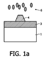
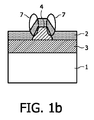
図1aには、有機材料6の堆積中の基板1が示されている。基板1は、透明な導体層3で覆われ、前記透明な導体層3には、分流線4が設けられる。この分流線4は、導体層3を覆う分流線の格子の一部であり、従って、付加的な配電チャネルとしての役割を果たす。
FIG. 1 a shows the
有機材料6は、表面積当たり一定の割合で透明な導体層3及び分流線4の上に堆積される。分流線は、この構成の表面の平面における障害となることから、分流線4上の有機材料6の成長は、この構成の残りの部分に比べて、薄くなる。上で既に述べたように、透明な導体層3に電圧が印加され、従って、分流線4に電圧が印加される場合には、分流線4の側部領域7における電界強度は、残りの部分における電界強度より高くなり、短絡形成及び装置故障を引き起こす。
The
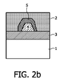
図2a及び2bに示されている本発明の実施例によれば、分流線4が、フォトレジストなどの電気絶縁材料5によって被覆されることから、分流線4の側部領域7における高い電界強度は解決される。このレジストは、電流が母線からOLEDの反対側電極(図示せず)の方へ引き込まれ得ることを防止する。このプロセスのためには、インクジェット印刷、グラビア印刷、スクリーン印刷などのような幾つかの堆積方法が使用可能である。
According to the embodiment of the invention shown in FIGS. 2a and 2b, the
一般的なフォトレジスト層は、十分な電気絶縁を供給するために、80nm程度の薄さで作成され得る。レーザ堆積分流線の場合は、有機層の層厚は、好ましくは、前記層の一般的な凸凹とほぼ同等である、又はそれより大きい。凸凹は、AFM(原子間力顕微鏡)測定において、100乃至500nm程度であると測定された。それ故、フォトレジスト層のためには、好ましくは、1乃至2μmの層厚が選択される。 A typical photoresist layer can be made as thin as 80 nm to provide sufficient electrical insulation. In the case of laser deposition shunt lines, the layer thickness of the organic layer is preferably approximately equal to or greater than the general irregularities of the layer. The unevenness was measured to be about 100 to 500 nm in AFM (Atomic Force Microscope) measurement. Therefore, a layer thickness of 1 to 2 μm is preferably selected for the photoresist layer.
ここに記載されている本発明の実施例によれば、堆積方法として、スクリーン印刷が選択された。この場合には、絶縁層5の最小線幅は、金属分流線4の最大幅に、金属パターンに対するスクリーン印刷パターンの位置合わせ精度をプラスすることで、与えられる。金属線の典型的な実験値は、80乃至150μmであり、位置合わせ精度は、200μm乃至300μm程度である。
According to the embodiment of the invention described here, screen printing was chosen as the deposition method. In this case, the minimum line width of the insulating
本発明の本実施例によれば、有機材料6の堆積後に、焼成ステップが加えられる。このステップは、2つの目的に適う。第1に、有機層と金属層との間の層接着が強化される。更に、有機層が、柔らかくなり、わずかに流れ、それによって、絶縁層5の小さな隙間を埋める。この焼成ステップは、20分乃至40分の期間の間、150℃と180℃との間の温度で行われる。
According to this embodiment of the invention, a baking step is added after the
本発明を、図面において図示し、上記の説明において詳細に説明しているが、このような図及び説明は、説明的なもの又は例示的なものとみなされるべきであって、限定するものとみなされるべきではない。本発明は、開示されている実施例に限定されない。 While the invention is illustrated in the drawings and has been described in detail in the foregoing description, such illustration and description are to be considered illustrative and exemplary and limited Should not be considered. The invention is not limited to the disclosed embodiments.
請求項に記載の発明を実施する当業者は、図面、明細及び添付の請求項の研究から、開示されている実施例に対する他の変形を、理解し、達成し得る。請求項において、「有する」という用語は、他の要素又はステップを除外せず、単数形表記は、複数の存在を除外しない。単に、特定の手段が、相互に異なる従属請求項において引用されているという事実は、これらの手段の組み合わせが有利になるように用いられることができないことを示すものではない。請求項におけるいかなる参照符号も、範囲を限定するものとして解釈されてはならない。 Those skilled in the art in practicing the claimed invention may understand and achieve other variations to the disclosed embodiments from a study of the drawings, the specification, and the appended claims. In the claims, the word “comprising” does not exclude other elements or steps, and the singular form does not exclude the presence of a plurality. The mere fact that certain measures are recited in mutually different dependent claims does not indicate that a combination of these measures cannot be used to advantage. Any reference signs in the claims should not be construed as limiting the scope.
Claims (14)
Applications Claiming Priority (3)
| Application Number | Priority Date | Filing Date | Title |
|---|---|---|---|
| EP08105477 | 2008-10-02 | ||
| EP08105477.7 | 2008-10-02 | ||
| PCT/IB2009/054209 WO2010038181A1 (en) | 2008-10-02 | 2009-09-25 | Oled device with covered shunt line |
Publications (1)
| Publication Number | Publication Date |
|---|---|
| JP2012504844A true JP2012504844A (en) | 2012-02-23 |
Family
ID=41480248
Family Applications (1)
| Application Number | Title | Priority Date | Filing Date |
|---|---|---|---|
| JP2011529658A Pending JP2012504844A (en) | 2008-10-02 | 2009-09-25 | OLED device with coated shunt line |
Country Status (8)
| Country | Link |
|---|---|
| US (1) | US20110186905A1 (en) |
| EP (1) | EP2332194A1 (en) |
| JP (1) | JP2012504844A (en) |
| KR (1) | KR20110082030A (en) |
| CN (1) | CN102171851B (en) |
| RU (1) | RU2507638C2 (en) |
| TW (1) | TW201028029A (en) |
| WO (1) | WO2010038181A1 (en) |
Cited By (4)
| Publication number | Priority date | Publication date | Assignee | Title |
|---|---|---|---|---|
| JP2012022878A (en) * | 2010-07-14 | 2012-02-02 | Nec Lighting Ltd | Organic electroluminescent illuminating device and manufacturing method thereof |
| WO2015173965A1 (en) * | 2014-05-16 | 2015-11-19 | パイオニア株式会社 | Light-emitting device |
| EP2983266A1 (en) | 2014-08-05 | 2016-02-10 | Panasonic Corporation | Power transmission device and wireless power transmission system |
| US11962163B2 (en) | 2014-08-05 | 2024-04-16 | Panasonic Holdings Corporation | Power transmission device and wireless power transmission system |
Families Citing this family (13)
| Publication number | Priority date | Publication date | Assignee | Title |
|---|---|---|---|---|
| JP2012009420A (en) * | 2010-05-21 | 2012-01-12 | Semiconductor Energy Lab Co Ltd | Light emitting device and illumination device |
| WO2012014759A1 (en) | 2010-07-26 | 2012-02-02 | Semiconductor Energy Laboratory Co., Ltd. | Light-emitting device, lighting device, and manufacturing method of light-emitting device |
| KR101972176B1 (en) * | 2010-08-23 | 2019-04-24 | 베이징 시아오미 모바일 소프트웨어 컴퍼니 리미티드 | Self-aligned coverage of opaque conductive areas |
| JPWO2012090903A1 (en) * | 2010-12-28 | 2014-06-05 | Necライティング株式会社 | ORGANIC ELECTROLUMINESCENT LIGHTING DEVICE AND MANUFACTURING METHOD FOR THE LIGHTING DEVICE |
| US8432095B2 (en) | 2011-05-11 | 2013-04-30 | Universal Display Corporation | Process for fabricating metal bus lines for OLED lighting panels |
| EP2736076A1 (en) * | 2012-11-23 | 2014-05-28 | Nederlandse Organisatie voor toegepast -natuurwetenschappelijk onderzoek TNO | Apparatus and method for manufacturing a layered product |
| KR101470515B1 (en) * | 2012-12-07 | 2014-12-09 | 주식회사 아모그린텍 | Organic thin film device and manufacturing mmethod thereof |
| US9484546B2 (en) | 2013-05-15 | 2016-11-01 | Universal Display Corporation | OLED with compact contact design and self-aligned insulators |
| CN105702875B (en) * | 2014-12-11 | 2018-04-27 | 财团法人工业技术研究院 | Light-emitting element, electrode structure and manufacturing method thereof |
| JP5999789B2 (en) * | 2015-03-02 | 2016-09-28 | Necライティング株式会社 | Method for manufacturing organic electroluminescent lighting device |
| DE102015119534A1 (en) * | 2015-11-12 | 2017-05-18 | Osram Oled Gmbh | Method for producing an optoelectronic component and optoelectronic component |
| KR101854701B1 (en) | 2016-05-31 | 2018-05-04 | 엘지디스플레이 주식회사 | Organic light emitting device and method of manufacturing the same |
| PL3784603T3 (en) | 2018-04-25 | 2022-05-23 | Autostore Technology AS | Container handling vehicle with first and second sections and larger wheel motors on two of the wheels in the second section |
Citations (11)
| Publication number | Priority date | Publication date | Assignee | Title |
|---|---|---|---|---|
| JPH10189244A (en) * | 1996-12-24 | 1998-07-21 | Casio Comput Co Ltd | Electro-luminescence panel |
| JP2000082588A (en) * | 1997-09-22 | 2000-03-21 | Fuji Electric Co Ltd | Organic light emitting element and manufacture therefor |
| JP2003096557A (en) * | 2001-09-25 | 2003-04-03 | Sanyo Electric Co Ltd | Apparatus and method for manufacturing organic el element |
| JP2003257663A (en) * | 2002-03-04 | 2003-09-12 | Rohm Co Ltd | Organic el display panel and its manufacturing method |
| WO2004077461A1 (en) * | 2003-02-26 | 2004-09-10 | Tdk Corporation | Multilayer unit containing electrode layer and dielectric layer |
| JP2005203196A (en) * | 2004-01-14 | 2005-07-28 | Fuji Electric Holdings Co Ltd | Passive matrix drive top emission type organic el element and its manufacturing method |
| JP2005276828A (en) * | 2004-03-23 | 2005-10-06 | Lg Electron Inc | Organic electroluminescence element and its manufacturing method |
| JP2006348274A (en) * | 2005-05-17 | 2006-12-28 | Sumitomo Chemical Co Ltd | Macromolecular composition for organic electroluminescence |
| JP2007242335A (en) * | 2006-03-07 | 2007-09-20 | Seiko Epson Corp | Manufacturing method of organic el device, and manufacturing apparatus of organic el device |
| JP2008004865A (en) * | 2006-06-26 | 2008-01-10 | Toyota Industries Corp | Organic electroluminescence display, and method for manufacturing the same |
| JP2008130355A (en) * | 2006-11-21 | 2008-06-05 | Toppan Printing Co Ltd | Method for manufacturing organic electroluminescence element |
Family Cites Families (18)
| Publication number | Priority date | Publication date | Assignee | Title |
|---|---|---|---|---|
| JPH05307997A (en) * | 1992-04-30 | 1993-11-19 | Pioneer Electron Corp | Organic electroluminescent element |
| US6111356A (en) * | 1998-04-13 | 2000-08-29 | Agilent Technologies, Inc. | Method for fabricating pixelated polymer organic light emitting devices |
| US6605826B2 (en) * | 2000-08-18 | 2003-08-12 | Semiconductor Energy Laboratory Co., Ltd. | Light-emitting device and display device |
| GB2388709A (en) * | 2002-05-17 | 2003-11-19 | Seiko Epson Corp | Circuit fabrication method |
| US6972261B2 (en) * | 2002-06-27 | 2005-12-06 | Xerox Corporation | Method for fabricating fine features by jet-printing and surface treatment |
| US7211461B2 (en) * | 2003-02-14 | 2007-05-01 | Semiconductor Energy Laboratory Co., Ltd. | Manufacturing apparatus |
| DE10324880B4 (en) * | 2003-05-30 | 2007-04-05 | Schott Ag | Process for the preparation of OLEDs |
| US7247986B2 (en) * | 2003-06-10 | 2007-07-24 | Samsung Sdi. Co., Ltd. | Organic electro luminescent display and method for fabricating the same |
| KR100741962B1 (en) * | 2003-11-26 | 2007-07-23 | 삼성에스디아이 주식회사 | Flat Panel Display |
| KR100549984B1 (en) * | 2003-12-29 | 2006-02-07 | 엘지.필립스 엘시디 주식회사 | Dual Panel Type Organic Electroluminescent Device and Method for Fabricating the same |
| RU2283855C2 (en) * | 2004-03-17 | 2006-09-20 | Самсунг Электроникс Ко., Лтд. | Luminescent semiconductor polymer material and a method for preparation thereof |
| WO2005106573A1 (en) * | 2004-04-30 | 2005-11-10 | Fuji Photo Film Co., Ltd. | Liquid crystal display and process for fabricating the same |
| KR100620851B1 (en) * | 2004-06-14 | 2006-09-19 | 엘지전자 주식회사 | Organic Electro-Luminescence Display Device And Fabricating Method Thereof |
| DE102005002837A1 (en) * | 2005-01-20 | 2006-08-17 | Schott Ag | Transparent electrode manufacturing method, e.g. for organic light emitting diode, involves providing data set that contains data representing structure of conductive paths to be manufactured, where paths form structured electrode layer |
| TWI284992B (en) * | 2005-01-21 | 2007-08-01 | Nat Univ Chung Cheng | Method of fabricating organic light emitting diode array |
| JP4591222B2 (en) * | 2005-06-09 | 2010-12-01 | セイコーエプソン株式会社 | Electro-optical device and image forming apparatus |
| JP4994727B2 (en) * | 2005-09-08 | 2012-08-08 | 株式会社リコー | Organic transistor active substrate, manufacturing method thereof, and electrophoretic display using the organic transistor active substrate |
| KR101376973B1 (en) * | 2007-04-27 | 2014-03-25 | 삼성디스플레이 주식회사 | Method of manufacturing thin film transistor substrate |
-
2009
- 2009-09-25 EP EP09787297A patent/EP2332194A1/en not_active Withdrawn
- 2009-09-25 JP JP2011529658A patent/JP2012504844A/en active Pending
- 2009-09-25 US US13/121,422 patent/US20110186905A1/en not_active Abandoned
- 2009-09-25 CN CN200980139286.9A patent/CN102171851B/en not_active Expired - Fee Related
- 2009-09-25 RU RU2011117180/28A patent/RU2507638C2/en not_active IP Right Cessation
- 2009-09-25 WO PCT/IB2009/054209 patent/WO2010038181A1/en active Application Filing
- 2009-09-25 KR KR1020117010043A patent/KR20110082030A/en active Search and Examination
- 2009-09-29 TW TW098133003A patent/TW201028029A/en unknown
Patent Citations (11)
| Publication number | Priority date | Publication date | Assignee | Title |
|---|---|---|---|---|
| JPH10189244A (en) * | 1996-12-24 | 1998-07-21 | Casio Comput Co Ltd | Electro-luminescence panel |
| JP2000082588A (en) * | 1997-09-22 | 2000-03-21 | Fuji Electric Co Ltd | Organic light emitting element and manufacture therefor |
| JP2003096557A (en) * | 2001-09-25 | 2003-04-03 | Sanyo Electric Co Ltd | Apparatus and method for manufacturing organic el element |
| JP2003257663A (en) * | 2002-03-04 | 2003-09-12 | Rohm Co Ltd | Organic el display panel and its manufacturing method |
| WO2004077461A1 (en) * | 2003-02-26 | 2004-09-10 | Tdk Corporation | Multilayer unit containing electrode layer and dielectric layer |
| JP2005203196A (en) * | 2004-01-14 | 2005-07-28 | Fuji Electric Holdings Co Ltd | Passive matrix drive top emission type organic el element and its manufacturing method |
| JP2005276828A (en) * | 2004-03-23 | 2005-10-06 | Lg Electron Inc | Organic electroluminescence element and its manufacturing method |
| JP2006348274A (en) * | 2005-05-17 | 2006-12-28 | Sumitomo Chemical Co Ltd | Macromolecular composition for organic electroluminescence |
| JP2007242335A (en) * | 2006-03-07 | 2007-09-20 | Seiko Epson Corp | Manufacturing method of organic el device, and manufacturing apparatus of organic el device |
| JP2008004865A (en) * | 2006-06-26 | 2008-01-10 | Toyota Industries Corp | Organic electroluminescence display, and method for manufacturing the same |
| JP2008130355A (en) * | 2006-11-21 | 2008-06-05 | Toppan Printing Co Ltd | Method for manufacturing organic electroluminescence element |
Cited By (6)
| Publication number | Priority date | Publication date | Assignee | Title |
|---|---|---|---|---|
| JP2012022878A (en) * | 2010-07-14 | 2012-02-02 | Nec Lighting Ltd | Organic electroluminescent illuminating device and manufacturing method thereof |
| WO2015173965A1 (en) * | 2014-05-16 | 2015-11-19 | パイオニア株式会社 | Light-emitting device |
| EP2983266A1 (en) | 2014-08-05 | 2016-02-10 | Panasonic Corporation | Power transmission device and wireless power transmission system |
| US9979235B2 (en) | 2014-08-05 | 2018-05-22 | Panasonic Corporation | Power transmission device and wireless power transmission system |
| US11056919B2 (en) | 2014-08-05 | 2021-07-06 | Panasonic Corporation | Power transmission device and wireless power transmission system |
| US11962163B2 (en) | 2014-08-05 | 2024-04-16 | Panasonic Holdings Corporation | Power transmission device and wireless power transmission system |
Also Published As
| Publication number | Publication date |
|---|---|
| TW201028029A (en) | 2010-07-16 |
| KR20110082030A (en) | 2011-07-15 |
| EP2332194A1 (en) | 2011-06-15 |
| WO2010038181A1 (en) | 2010-04-08 |
| CN102171851B (en) | 2014-05-07 |
| CN102171851A (en) | 2011-08-31 |
| RU2011117180A (en) | 2012-11-10 |
| RU2507638C2 (en) | 2014-02-20 |
| US20110186905A1 (en) | 2011-08-04 |
Similar Documents
| Publication | Publication Date | Title |
|---|---|---|
| JP2012504844A (en) | OLED device with coated shunt line | |
| TWI602333B (en) | Optoelectronic devices and processes for fabricating optoelectronic devices | |
| KR100672316B1 (en) | Oled device | |
| US8497626B2 (en) | Large area light emitting diode light source | |
| KR20080032128A (en) | Organic based device and method for manufacture thereof | |
| JP6223360B2 (en) | OLED element and its manufacture | |
| KR20110074518A (en) | Method for producing an organic radiation-emitting component and organic radiation-emitting component | |
| US8536779B2 (en) | Electroluminescent device with protective means for divide areas | |
| US20120295372A1 (en) | Method of maskless manufacturing of oled devices | |
| JP5656975B2 (en) | Photoelectric device and manufacturing method thereof | |
| JPWO2011136205A1 (en) | ORGANIC ELECTROLUMINESCENT LIGHTING DEVICE AND ITS MANUFACTURING METHOD | |
| KR20130061138A (en) | Method of manufacturing an oled device with spatially isolated light-emitting areas | |
| US20180374423A1 (en) | Light-Emitting Device | |
| US8816335B2 (en) | Method for creating serially-connected OLED devices | |
| US20170301874A1 (en) | Organic el panel and method for producing same | |
| US9882159B2 (en) | Voltage-light conversion device | |
| WO2011101766A1 (en) | Oled device and method of manufacturing the same | |
| KR20090112700A (en) | Radiationemitting apparatus?and method for the production of a radiationemitting apparatus | |
| US20170317311A1 (en) | Optoelectronic device with a fuse | |
| JP2023108047A (en) | Light-emitting device | |
| WO2012127400A1 (en) | Oled with a shunting layer |
Legal Events
| Date | Code | Title | Description |
|---|---|---|---|
| A621 | Written request for application examination |
Free format text: JAPANESE INTERMEDIATE CODE: A621 Effective date: 20120924 |
|
| A977 | Report on retrieval |
Free format text: JAPANESE INTERMEDIATE CODE: A971007 Effective date: 20130611 |
|
| A131 | Notification of reasons for refusal |
Free format text: JAPANESE INTERMEDIATE CODE: A131 Effective date: 20130613 |
|
| A521 | Request for written amendment filed |
Free format text: JAPANESE INTERMEDIATE CODE: A523 Effective date: 20130912 |
|
| A02 | Decision of refusal |
Free format text: JAPANESE INTERMEDIATE CODE: A02 Effective date: 20131203 |
|
| A521 | Request for written amendment filed |
Free format text: JAPANESE INTERMEDIATE CODE: A523 Effective date: 20140327 |
|
| A911 | Transfer to examiner for re-examination before appeal (zenchi) |
Free format text: JAPANESE INTERMEDIATE CODE: A911 Effective date: 20140416 |
|
| A912 | Re-examination (zenchi) completed and case transferred to appeal board |
Free format text: JAPANESE INTERMEDIATE CODE: A912 Effective date: 20140606 |