JP6223360B2 - OLED element and its manufacture - Google Patents
OLED element and its manufacture Download PDFInfo
- Publication number
- JP6223360B2 JP6223360B2 JP2014555367A JP2014555367A JP6223360B2 JP 6223360 B2 JP6223360 B2 JP 6223360B2 JP 2014555367 A JP2014555367 A JP 2014555367A JP 2014555367 A JP2014555367 A JP 2014555367A JP 6223360 B2 JP6223360 B2 JP 6223360B2
- Authority
- JP
- Japan
- Prior art keywords
- insulating material
- layer
- conductive coating
- conductive
- patterning
- Prior art date
- Legal status (The legal status is an assumption and is not a legal conclusion. Google has not performed a legal analysis and makes no representation as to the accuracy of the status listed.)
- Active
Links
Images


Classifications
-
- H—ELECTRICITY
- H10—SEMICONDUCTOR DEVICES; ELECTRIC SOLID-STATE DEVICES NOT OTHERWISE PROVIDED FOR
- H10K—ORGANIC ELECTRIC SOLID-STATE DEVICES
- H10K50/00—Organic light-emitting devices
- H10K50/80—Constructional details
- H10K50/84—Passivation; Containers; Encapsulations
- H10K50/844—Encapsulations
-
- H—ELECTRICITY
- H10—SEMICONDUCTOR DEVICES; ELECTRIC SOLID-STATE DEVICES NOT OTHERWISE PROVIDED FOR
- H10K—ORGANIC ELECTRIC SOLID-STATE DEVICES
- H10K50/00—Organic light-emitting devices
-
- H—ELECTRICITY
- H10—SEMICONDUCTOR DEVICES; ELECTRIC SOLID-STATE DEVICES NOT OTHERWISE PROVIDED FOR
- H10K—ORGANIC ELECTRIC SOLID-STATE DEVICES
- H10K71/00—Manufacture or treatment specially adapted for the organic devices covered by this subclass
- H10K71/621—Providing a shape to conductive layers, e.g. patterning or selective deposition
-
- H—ELECTRICITY
- H10—SEMICONDUCTOR DEVICES; ELECTRIC SOLID-STATE DEVICES NOT OTHERWISE PROVIDED FOR
- H10K—ORGANIC ELECTRIC SOLID-STATE DEVICES
- H10K50/00—Organic light-emitting devices
- H10K50/80—Constructional details
- H10K50/805—Electrodes
- H10K50/81—Anodes
- H10K50/816—Multilayers, e.g. transparent multilayers
-
- H—ELECTRICITY
- H10—SEMICONDUCTOR DEVICES; ELECTRIC SOLID-STATE DEVICES NOT OTHERWISE PROVIDED FOR
- H10K—ORGANIC ELECTRIC SOLID-STATE DEVICES
- H10K50/00—Organic light-emitting devices
- H10K50/80—Constructional details
- H10K50/805—Electrodes
- H10K50/82—Cathodes
- H10K50/828—Transparent cathodes, e.g. comprising thin metal layers
-
- H—ELECTRICITY
- H10—SEMICONDUCTOR DEVICES; ELECTRIC SOLID-STATE DEVICES NOT OTHERWISE PROVIDED FOR
- H10K—ORGANIC ELECTRIC SOLID-STATE DEVICES
- H10K71/00—Manufacture or treatment specially adapted for the organic devices covered by this subclass
Description
本発明は、OLED素子の製造方法を開示する。また、本発明はOLED素子の製造のための半製品、及びOLED素子に関する。 The present invention discloses a method for manufacturing an OLED element. The invention also relates to a semi-finished product for the manufacture of OLED elements and OLED elements.
OLED素子及び無機EL素子、すなわち、有機ELフィルム及び無機ELフィルムは、2つの電極層間の発光層が電極層によって電気的に刺激されて発光するという効果に基づく。無機ELフィルムにおいて、2つの電極は互いに電気的に絶縁され、コンデンサの両半分として機能する。このコンデンサに交流電圧をかけると、コンデンサは発光層を刺激して発光させる電界を発する。一方、OLED素子、すなわち有機ELフィルムにおいては、一方の電極から他方の電極に直流が流れることにより直流が発光層を通過し、やはり発光させる。 The OLED element and the inorganic EL element, that is, the organic EL film and the inorganic EL film are based on the effect that the light emitting layer between the two electrode layers is electrically stimulated by the electrode layer to emit light. In the inorganic EL film, the two electrodes are electrically insulated from each other and function as both halves of the capacitor. When an AC voltage is applied to the capacitor, the capacitor generates an electric field that stimulates the light emitting layer to emit light. On the other hand, in an OLED element, that is, an organic EL film, a direct current flows from one electrode to the other electrode, whereby the direct current passes through the light emitting layer and emits light.
OLED素子の製造は、2つの電極層(アノード及びカソード)及び有機発光層等の異なる機能層を高精度で形成(又は付加)する工程を要する、一般的には時間がかかるプロセスである。十分な寿命を実現するためには、OLED素子は外的影響に対して適切に密封されなければならず、また、十分な耐湿性及び安定性を有するキャリア上に構築されなければならない。好ましくは、全体として可撓性のOLED素子を提供するために、このキャリアは可撓性である。これは、第1に、厚い照明ソリューションを避けなければならないようなあらゆる環境において適用できる程度にOLED素子が非常に薄いという利点を有する。第2に、可撓性のOLED素子は、OLED素子が完全に平坦な平面に沿ってではなく、曲面等に沿って配置される場合にも適用できる。 Manufacturing an OLED element is a time-consuming process that generally requires a step of forming (or adding) different functional layers such as two electrode layers (anode and cathode) and an organic light emitting layer with high accuracy. In order to achieve a sufficient lifetime, the OLED element must be properly sealed against external influences and must be built on a carrier that has sufficient moisture resistance and stability. Preferably, the carrier is flexible in order to provide an overall flexible OLED element. This first has the advantage that the OLED element is so thin that it can be applied in any environment where thick lighting solutions must be avoided. Secondly, the flexible OLED element can also be applied when the OLED element is arranged along a curved surface or the like instead of along a completely flat plane.
可撓性のキャリア基板を実現する1つの選択可能なソリューションは、US6,911,666B2に示されるように金属フィルム又はホイルを使用することである。しかし、これは、OLEDの機能的な理由から回避しなければならない大きな欠点を有する。すなわち、金属フィルム又はホイルは一般的に導電性基板として特徴付けることができ、これは、それら自身の導電性が上記したようなOLEDデバイスの他の機能層に危険に干渉するおそれがあることを意味する。本質的に、このような導電性キャリア基板の導電性はショートをもたらす可能性がある。アノード及びカソードの両方がキャリア基板上の導体パッドを介して電気的に接触されなければならないので、電極の一方の導体パッドを他方の電極からガルバニック絶縁するよう実現する必要がある。 One alternative solution to realize a flexible carrier substrate is to use a metal film or foil as shown in US 6,911,666 B2. However, this has major drawbacks that must be avoided for functional reasons of OLEDs. That is, metal films or foils can generally be characterized as conductive substrates, which means that their own conductivity can potentially interfere with other functional layers of OLED devices as described above. To do. In essence, the conductivity of such a conductive carrier substrate can cause a short circuit. Since both the anode and cathode must be in electrical contact via conductor pads on the carrier substrate, it is necessary to realize that one conductor pad of the electrode is galvanically isolated from the other electrode.
これは、導電性キャリア基板の全表面にかけてキャリア基板上に非導電性コーティングを形成して、更に非導電性コーティングの上に分離された導電性コーティングを形成することによって、又は、1つの電極導体パッドの領域内に絶縁材料を局所的に堆積させることによって実現することができる。1つ目のケースの場合、非導電性コーティング層にわたってのみ電流を流すことができる。言い換えれば、キャリア基板の導電性は電流を輸送するために使用されない。また、このソリューションは材料の選択を限定し、大面積OLED素子においては比較的厚い層構造をもたらす。2つ目のケースの場合、絶縁材料上に導体パッドとして無機材料を堆積させなければならず、また、OLED素子の内部電極及び外部電源と接触させなければならず、これは、導体パッドがOLED素子の封止を横断することを意味する。また、このような絶縁層のパターニング堆積又はパターニング後処理は高コストであり、比較的非効率的である。有機絶縁体は耐湿層として機能することができず、よって比較的早期にOLED素子に機能的な欠陥を生じさせるため、有機絶縁体は使用することができない。 This can be done by forming a non-conductive coating on the carrier substrate over the entire surface of the conductive carrier substrate and then forming a separate conductive coating on the non-conductive coating, or one electrode conductor This can be achieved by locally depositing an insulating material in the region of the pad. In the first case, current can only flow across the non-conductive coating layer. In other words, the conductivity of the carrier substrate is not used to transport current. This solution also limits the choice of materials and results in a relatively thick layer structure in large area OLED devices. In the second case, the inorganic material must be deposited as a conductor pad on the insulating material, and it must be in contact with the internal electrode of the OLED element and an external power source, where the conductor pad is an OLED. This means traversing the element seal. Also, such patterning or post-patterning processing of the insulating layer is costly and relatively inefficient. The organic insulator cannot function as a moisture-resistant layer, and therefore causes a functional defect in the OLED element relatively early, so that the organic insulator cannot be used.
したがって、本発明の目的は、導電性キャリア基板を有するOLEDをより効率的に提供する可能性、特に、従来必要とされたものより単純なコーティング工程による製造を提供することである。 Accordingly, it is an object of the present invention to provide the possibility of providing an OLED with a conductive carrier substrate more efficiently, in particular the manufacture by a simpler coating process than previously required.
本発明の目的は、請求項1に係る方法、請求項14に係る半製品、及び請求項15に係るOLED素子によって達成される。
The object of the invention is achieved by a method according to claim 1, a semi-finished product according to claim 14 and an OLED element according to
本発明によれば、上記したような方法は、少なくとも、
−a)第1のキャリア表面及び第2のキャリア表面を有する導電性キャリア基板を提供するステップと、
−b)少なくとも第1のキャリア表面の全領域にかけて絶縁材料のパターニングされた層を構築するステップであって、好ましくは、絶縁材料の層は第1のキャリア表面を完全に覆い、また、絶縁材料の層は第1のキャリア表面の反対側に面する絶縁材料の層の上面から第1のキャリア表面に電気的にアクセス可能なように複数の孔によってパターニングされる、ステップと、
−c)絶縁材料の上面にパターニングされた導電性コーティングを構築するステップであって、導電性コーティングは、孔に入り込み、絶縁材料の全領域を覆い、また、導電性コーティング内に複数の個別の第1の電極領域が形成されるようパターニングされ、また、好ましくは導電性コーティングは実質的に絶縁材料を完全に覆う、ステップと、
−d)少なくとも1つの第1の電極領域上に有機発光層を形成するステップと、
−e)有機発光層上に第2の電極層を形成するステップと
を含む。
According to the invention, the method as described above is at least
-A) providing a conductive carrier substrate having a first carrier surface and a second carrier surface;
-B) constructing a patterned layer of insulating material over at least the entire area of the first carrier surface, preferably the layer of insulating material completely covers the first carrier surface, and the insulating material The layer of is patterned with a plurality of holes so that the first carrier surface is electrically accessible from the top surface of the layer of insulating material facing away from the first carrier surface;
-C) building a patterned conductive coating on the top surface of the insulating material, the conductive coating entering the hole, covering the entire area of the insulating material, and a plurality of individual coatings within the conductive coating Patterning to form a first electrode region, and preferably the conductive coating substantially completely covers the insulating material;
-D) forming an organic light emitting layer on the at least one first electrode region;
-E) forming a second electrode layer on the organic light emitting layer.
実際には導電性キャリア基板は全ての選択可能な材料を含み得るが、好ましくは金属層を含む。最も好ましくは、導電性キャリア基板は、非常に薄い厚さから(すなわち、25μmから)、硬いほぼ非可塑性の(すなわち、ほぼ曲がらない)キャリア基板を提供する厚さまで、実質的にあらゆる強度で利用可能な標準材料を構成することから、キャリア基板として使用可能な特に取り扱いやすい基材である金属フィルム又は金属ホイルから主に又は完全に構成される。しかし、OLED素子が可塑性のOLED素子としても設計できるよう、導電性キャリア基板が可塑性であることが好ましい。このような金属層又はフィルムは、例えばアルミニウムを含んでもよい。 In practice, the conductive carrier substrate may comprise any selectable material, but preferably comprises a metal layer. Most preferably, the conductive carrier substrate is utilized at virtually any strength, from very thin thicknesses (ie, 25 μm) to thicknesses that provide a hard, substantially non-plastic (ie, substantially unbent) carrier substrate. Because it constitutes a possible standard material, it consists mainly or completely of a metal film or metal foil, which is a particularly easy-to-handle substrate that can be used as a carrier substrate. However, the conductive carrier substrate is preferably plastic so that the OLED element can also be designed as a plastic OLED element. Such a metal layer or film may comprise, for example, aluminum.
第1のキャリア表面に形成される絶縁材料の層に関しては、この層は好ましくは無機材料を、最も好ましくは無機層を含む。 With respect to the layer of insulating material formed on the first carrier surface, this layer preferably comprises an inorganic material, most preferably an inorganic layer.
全領域の定義に関しては、これは、(絶縁材料の場合)端部において可能な限り小さいマージン(すなわち、最大で導電性キャリア基板の全平面範囲の10%)を有して導電性キャリア基板の範囲を実質的に覆う単一の領域を意味し、又は、(パターニングされた導電性コーティングの場合)OLED素子の発光領域の最大範囲を実質的に定める。しかし、絶縁材料の全領域は、導電性キャリア基板の第1の表面の全体を覆うことが好ましい。 With respect to the definition of the whole area, this means that (for insulating materials) the margin of the conductive carrier substrate with the smallest possible margin at the edge (ie up to 10% of the total planar area of the conductive carrier substrate). It means a single area that substantially covers the area or, in the case of a patterned conductive coating, substantially defines the maximum area of the light emitting area of the OLED element. However, the entire region of insulating material preferably covers the entire first surface of the conductive carrier substrate.
第1の電極領域は好ましくはOLED素子のアノードとして実現され、よって第2の電極層は好ましくはカソードとして実現される。第2の電極層は少なくとも有機発光層上に配置され、これは、第2の電極層が有機発光層の範囲を越えたより広い領域を覆ってもよいことを示唆する。 The first electrode region is preferably realized as the anode of the OLED element, and thus the second electrode layer is preferably realized as the cathode. The second electrode layer is disposed at least on the organic light emitting layer, suggesting that the second electrode layer may cover a wider area beyond the range of the organic light emitting layer.
第1の表面及び第2の表面の両方向から光を発する両面OLED素子が製造されるよう、キャリア基板の第2の表面において同様に同じプロセスを繰り返し実行してもよい。 The same process may be repeated in the same way on the second surface of the carrier substrate so that a double-sided OLED device emitting light from both directions of the first surface and the second surface is produced.
本質的に、この方法は、(標準的な)導電性キャリア材料をその導電性にも関わらず、また接触目的のためにその導電性を実際に利用して如何に使用するかの容易な可能性を提供する。したがって、この方法は、導電性キャリア基板を第1の電極への電力供給のための接触領域として使用することを可能にする。これにより、複数の孔は複数の供給点において第1の電極領域に電流を供給することを可能にする。これは、第1の電極領域の平面範囲全体にかけてのより均等な電流分布を提供する。OLED素子においては実際に電流が一方の電極から発光層を介して他方の電極に流れるので、これは、OLED素子において特に重要である。一方、上述したような無機ELフィルムにおいては、2つの電極間のあらゆる接触点において必要なAC電圧を供給することにより、はるかに容易に電界を生成することができる。したがって、無機ELにおいて実質的に自動的に均質な配光を達成することができる。よって、本発明に係る方法は、50x50〜300x300mm等のサイズの大きなOLED素子の製造において特に有用である。 In essence, this method makes it easy to use a (standard) conductive carrier material, regardless of its conductivity, and in practice using its conductivity for contact purposes. Provide sex. This method thus makes it possible to use the conductive carrier substrate as a contact area for supplying power to the first electrode. This allows the plurality of holes to supply current to the first electrode region at a plurality of supply points. This provides a more even current distribution over the entire planar area of the first electrode region. This is particularly important in an OLED element, because in an OLED element, current actually flows from one electrode to the other electrode through the light emitting layer. On the other hand, in the inorganic EL film as described above, an electric field can be generated much more easily by supplying a necessary AC voltage at every contact point between two electrodes. Accordingly, a homogeneous light distribution can be achieved substantially automatically in the inorganic EL. Therefore, the method according to the present invention is particularly useful in the manufacture of large OLED elements such as 50 × 50 to 300 × 300 mm.
上記プロセスから得られるのは、
−a)第1のキャリア表面及び第2のキャリア表面を有する導電性キャリア基板と、
−b)少なくとも第1のキャリア表面の全領域上にコーティングされた絶縁材料の層であって、好ましくは、絶縁材料の層は第1のキャリア表面を完全に覆い、また、絶縁材料の層は第1のキャリア表面の反対側に面する絶縁材料の層の上面から第1のキャリア表面に電気的にアクセス可能なように複数の孔を含むパターンを有する、絶縁材料の層と、
−c)絶縁材料の上面における導電性コーティングであって、導電性コーティングは孔内に入り込み、絶縁材料の全領域を覆い、また、導電性コーティング内に複数の個別の第1の電極領域が形成されるようなパターンを有する、導電性コーティングと、
−d)少なくとも1つの第1の電極領域上の有機発光層と、
−e)有機発光層上に形成された第2の電極層と
を含む、本発明に係るOLED素子である。
The above process results in
-A) a conductive carrier substrate having a first carrier surface and a second carrier surface;
-B) a layer of insulating material coated over at least the entire area of the first carrier surface, preferably the layer of insulating material completely covers the first carrier surface, and the layer of insulating material is A layer of insulating material having a pattern including a plurality of holes for electrical access to the first carrier surface from an upper surface of the layer of insulating material facing away from the first carrier surface;
-C) a conductive coating on the top surface of the insulating material, wherein the conductive coating penetrates into the holes and covers the entire area of the insulating material, and a plurality of individual first electrode regions are formed in the conductive coating A conductive coating having a pattern such as
-D) an organic light emitting layer on at least one first electrode region;
-E) An OLED device according to the present invention comprising a second electrode layer formed on the organic light emitting layer.
OLED素子の所望の特定のアウトレットに応じて、追加の層、特に接触層、絶縁層等を加えてもよい。 Depending on the desired specific outlet of the OLED element, additional layers, in particular contact layers, insulating layers, etc. may be added.
また、標準的な導電性キャリア基板の使用は標準的な半製品の製造も可能にし、半製品は、その後特定のニーズに応じて、すなわち、本発明に係るOLED素子の特定の設計に応じてエンド仕上げすることができる。したがって、大量の半製品を組み立て式でつくり(prefabricate)、その後それらの半製品をもとに少量の特定の(本発明に係る)OLED素子を、例えば特定のコンシューマニーズに基づいて製造することができる。 The use of a standard conductive carrier substrate also allows the production of a standard semi-finished product, which is then according to specific needs, ie according to the specific design of the OLED device according to the invention. End finish can be done. Thus, it is possible to prefabricate a large number of semi-finished products and then manufacture a small amount of specific (according to the invention) OLED elements based on these semi-finished products, for example based on specific consumer needs it can.
したがって、本発明は更に、OLED素子の生産のための半製品であって、
−a)第1のキャリア表面及び第2のキャリア表面を有する導電性キャリア基板と、
−b)少なくとも第1のキャリア表面の全領域上にコーティングされた絶縁材料の層であって、絶縁材料の層は、好ましくは第1のキャリア表面を絶縁材料によって完全に覆うようにコーティングされ、また、絶縁材料の層は、第1のキャリア表面の反対側に面する絶縁材料の層の上面から第1のキャリア表面への電気的アクセスが可能なように複数の孔を含むパターンを有する、絶縁材料の層と、
−c)孔内に入り込み、絶縁材料の全領域を覆う、絶縁材料の上面における導電性コーティングであって、好ましくは絶縁材料を完全に覆う導電性コーティングと
を含む、半製品にも関する。
Thus, the present invention is further a semi-finished product for the production of OLED elements,
-A) a conductive carrier substrate having a first carrier surface and a second carrier surface;
-B) a layer of insulating material coated over at least the entire area of the first carrier surface, wherein the layer of insulating material is preferably coated so that the first carrier surface is completely covered by the insulating material; In addition, the layer of insulating material has a pattern including a plurality of holes so as to allow electrical access to the first carrier surface from the top surface of the layer of insulating material facing away from the first carrier surface. A layer of insulating material;
C) also relates to a semi-finished product, comprising a conductive coating on the top surface of the insulating material that penetrates into the hole and covers the entire area of the insulating material, preferably completely covering the insulating material.
この文脈において(そして一般的に本発明の文脈において)、導電性コーティングは好ましくは透明又は半透明の導電性コーティングである。このようにすることで、絶縁層内の孔を光学的に(特に好ましくは自動的に)検出することができ、これは、後の形成、アブレーション、及び/又は切断ステップにおいて、検出されたパターンをオリエンテーション又は見当マークとして用いるために非常に好ましい。あるいは、不透明な導電性コーティングを施す場合、見当マークとして使用するための孔の位置は、(孔の位置による)導電性コーティングの表面内の凹凸を検出することによって検出できる。これも不可能な場合、規則的な孔パターンを使用して、単一の孔(又は複数の孔)の位置をマークするか又は記憶することにより、あらゆる孔の位置を再計算して孔の位置を定めることもできる。 In this context (and generally in the context of the present invention), the conductive coating is preferably a transparent or translucent conductive coating. In this way, the holes in the insulating layer can be detected optically (especially preferably automatically) by detecting the detected pattern in a subsequent forming, ablation and / or cutting step. Is highly preferred for use as an orientation or register mark. Alternatively, when applying an opaque conductive coating, the position of the hole for use as a registration mark can be detected by detecting irregularities in the surface of the conductive coating (depending on the position of the hole). If this is also not possible, use a regular hole pattern to recalculate the position of any hole by marking or remembering the position of a single hole (or holes). The position can also be determined.
場合によっては、後に半製品に基づいて作成され得る大量のOLED素子の製造にとって厳密に何が必要な標準要素と考えられるかに応じて、本発明に係るOLED素子の文脈において述べられた要素より多くが半製品に含まれてもよい。 Depending on what is considered to be the standard element that is strictly necessary for the production of large quantities of OLED elements that can later be made on the basis of semi-finished products, the elements mentioned in the context of the OLED element according to the invention Many may be included in the semi-finished product.
したがって、本発明に係る方法は好ましくは、少なくともステップa)及びb)、並びに、導電性コーティングが孔内に入り込み、絶縁材料の全領域を覆うよう絶縁材料の上面に導電性コーティングを構築するステップを含むプロセスにおいて半製品を生産することによって実現され、半製品は後に別個のプロセスにおいて処理される。この場合、別個のプロセスはステップc)〜e)から選択される残りのステップを含む。 Thus, the method according to the invention preferably comprises at least steps a) and b) and the step of constructing a conductive coating on the top surface of the insulating material so that the conductive coating enters the hole and covers the entire area of the insulating material. The semi-finished product is later processed in a separate process. In this case, the separate process includes the remaining steps selected from steps c) -e).
従属請求項及び下記の説明は、本発明の特に好適な実施形態及び特徴を開示する。請求項の特徴を適切に組み合わせることによって他の実施形態を実現してもよい。1つの請求項カテゴリの文脈において記載された特徴は、他の請求項カテゴリに等しく適用できる。 The dependent claims and the following description disclose particularly preferred embodiments and features of the invention. Other embodiments may be implemented by appropriately combining the features of the claims. Features described in the context of one claim category are equally applicable to other claim categories.
好ましい一実施形態によれば、構築ステップb)は、
−b1)絶縁材料の層によって少なくとも第1のキャリア表面の全領域をコーティングするステップと、
−b2)絶縁材料の層内に複数の孔を形成することによって絶縁材料の層をパターニングするステップと
を含み、且つ/又は、構築ステップc)は、
−c1)導電性コーティングが孔に入り込み、絶縁材料の全領域を覆うよう、絶縁材料の上面に導電性コーティングを形成するステップと、
−c2)複数の個別の第1の電極領域が導電性コーティング内に形成されるよう導電性コーティングをパターニングするステップとを含む。
According to one preferred embodiment, the construction step b)
-B1) coating at least the entire area of the first carrier surface with a layer of insulating material;
-B2) patterning the layer of insulating material by forming a plurality of holes in the layer of insulating material, and / or the building step c) comprises:
-C1) forming a conductive coating on the top surface of the insulating material so that the conductive coating enters the hole and covers the entire area of the insulating material;
-C2) patterning the conductive coating such that a plurality of individual first electrode regions are formed in the conductive coating.
したがって、ステップb)及び/又はc)の一方又は両方をサブステップに分割することができる。ステップb)は、第1の表面全体に(場合によっては端部に多少のマージンを残して)コーティングが施される第1のステップb1)を含んでもよい。コーティング処理中の絶縁材料のパターニングは比較的難しい可能性があるので、このような全コーティングステップb1)は特に実行しやすい。この場合、絶縁材料のパターニングはコーティングステップb1)の後に実行される。まとめられたコーティング/パターニング処理は短時間で済むがより複雑になる一方、コーティングステップb1)及びパターニングステップb2)の両ステップはともにそれら自体は比較的単純なステップである。 Thus, one or both of steps b) and / or c) can be divided into sub-steps. Step b) may comprise a first step b1) in which the entire first surface is coated (possibly leaving some margin at the edges). Since the patterning of the insulating material during the coating process can be relatively difficult, such an entire coating step b1) is particularly easy to perform. In this case, the patterning of the insulating material is performed after the coating step b1). While the combined coating / patterning process is short but more complicated, both the coating step b1) and the patterning step b2) are both relatively simple steps themselves.
絶縁材料に関して説明した方法と同様に2つのサブステップに分割できる導電性コーティングの形成にも同じ理論が適用できる。同様に、パターニングステップc2)は形成ステップc1)とは別個のステップであり、全体的な単純化、及びステップc1)及びc2)それぞれのより容易な取扱い等の同じ好適な効果を有する。 The same theory can be applied to the formation of a conductive coating that can be divided into two sub-steps in the same manner as described for the insulating material. Similarly, the patterning step c2) is a separate step from the formation step c1) and has the same preferred effects such as overall simplification and easier handling of each of steps c1) and c2).
少なくとも1つの個別の第1の電極領域が絶縁材料の複数の孔を介して導電性キャリア基板とガルバニック接触するよう導電性コーティングのパターニングが実行される場合、特に好適であることが証明された。これは、第1の電極領域が単一の接触領域(すなわち、孔)を介してではなく、複数のかかる接触領域を介して給電されることを意味する。特に、OLED素子のより均等な発光効果が得られるので、これは大面積OLED素子を製造する場合に好適であり、OLED素子が大きければ大きいほど、電極に大面積にわたって供給することが大きな意味を持つ。 It has proved particularly suitable when the patterning of the conductive coating is carried out such that at least one individual first electrode region is in galvanic contact with the conductive carrier substrate via a plurality of holes of insulating material. This means that the first electrode region is fed through a plurality of such contact regions rather than through a single contact region (ie, a hole). In particular, since a more uniform light emitting effect of the OLED element can be obtained, this is suitable when manufacturing a large area OLED element, and the larger the OLED element, the greater the significance of supplying the electrode over a large area. Have.
本発明の他の非常に好適な実施形態によれば、導電性コーティングのパターニング後、導電性コーティング内のギャップが絶縁材料、好ましくは印刷絶縁材料によって充填される。個別の第1の電極領域を絶縁するこれらのギャップは、導電性コーティングによって規定される平面に沿って第1の電極領域を囲う周辺領域から導電性コーティングをパターニングすることによって得られる。 According to another highly preferred embodiment of the invention, after patterning the conductive coating, the gap in the conductive coating is filled with an insulating material, preferably a printed insulating material. These gaps that insulate the individual first electrode regions are obtained by patterning the conductive coating from a peripheral region surrounding the first electrode region along a plane defined by the conductive coating.
ステップb)において先に使用されたものと同じ絶縁材料を使用することができるが、ステップb)の上記絶縁材料とは異なる印刷絶縁材料を使用してもよい。これは、ここでの絶縁材料はOLED素子の内部と外部を接続しないので、第1の表面上に付加される絶縁材料が好ましくは耐水バリアとして使用可能である一方、導電性コーティングギャップを充填する絶縁材料は必ずしもそうである必要がないという事実による。このような追加の絶縁ステップは、導電性コーティング上に他の(特に導電性の)層が堆積された場合、導電性コーティングの各領域間に電気的接続が存在しないという利点を有する。これは、発光領域の規定を著しく単純化する。 The same insulating material previously used in step b) can be used, but a printed insulating material different from the above insulating material in step b) may be used. This is because the insulating material here does not connect the inside and the outside of the OLED element, so that the insulating material added on the first surface can preferably be used as a water resistant barrier while filling the conductive coating gap. Due to the fact that the insulating material does not necessarily have to be. Such an additional insulating step has the advantage that there are no electrical connections between the regions of the conductive coating when other (especially conductive) layers are deposited on the conductive coating. This greatly simplifies the definition of the light emitting area.
一般的に、第2の電極層は、第1の電極領域、及び第1の電極領域とガルバニック接触する全ての導電層から電気的に絶縁されなければならない。例えば、これは、導電性コーティングのパターンによって定められる切断線に沿って、すなわち、OLED素子の発光領域の端部に沿ってOLED素子の全層を切断することによって達成できる。このようにすることで、第2の電極層は、導電性コーティングと接触するような領域まで(OLED素子の主要広がり面に沿って)延在しないので、第2の電極層は第1の電極層から完全に電気的に絶縁される。このような切断が望ましくない場合、導電性コーティングが第2の電極層とガルバニック接触するような接触領域において、導電性コーティングと導電性キャリア基板との間のコンタクトが除去されることが好ましい。例えば、第2の電極層が一方向において発光層の境界を(OLED素子の主要広がり面に沿って)越えて延在する一方、反対の方向においては、発光層の境界上までのみ延在してもよい。このような場合、導電性コーティングと導電性キャリア基板との間のコンタクトは、好ましくは第2の電極が発光層の境界を越えて延在する領域においてのみ取り除かれる。第2の電極層が二方向以上において発光層の境界を越えて(OLED素子の主要広がり面に沿って)延在する場合、例えば、場合によっては導電性コーティングの全範囲にわたって延在する場合、導電性コーティングと導電性キャリア基板との間のコンタクトは、発光層によって間接的に覆われていない孔によって規定される全接触領域において取り除かれなければならない。この実施形態は、第2の電極層の平面範囲の実質的にいずれの位置においても第2の電極層に接触可能にするという点で有利である。 In general, the second electrode layer must be electrically isolated from the first electrode region and all conductive layers in galvanic contact with the first electrode region. For example, this can be achieved by cutting the entire layer of the OLED element along a cutting line defined by the pattern of the conductive coating, ie along the edge of the light emitting area of the OLED element. In this way, the second electrode layer does not extend to a region in contact with the conductive coating (along the main spreading surface of the OLED element), so that the second electrode layer is the first electrode. Fully electrically isolated from the layers. If such cutting is not desired, the contact between the conductive coating and the conductive carrier substrate is preferably removed in the contact area where the conductive coating is in galvanic contact with the second electrode layer. For example, the second electrode layer extends in one direction beyond the boundary of the light emitting layer (along the main spreading surface of the OLED element), while in the opposite direction extends only up to the boundary of the light emitting layer. May be. In such a case, the contact between the conductive coating and the conductive carrier substrate is preferably removed only in the region where the second electrode extends beyond the boundary of the light emitting layer. If the second electrode layer extends beyond the boundary of the light emitting layer in more than one direction (along the main spreading surface of the OLED element), for example, in some cases it extends over the entire range of the conductive coating, The contact between the conductive coating and the conductive carrier substrate must be removed in the entire contact area defined by the holes that are not indirectly covered by the light emitting layer. This embodiment is advantageous in that it allows contact with the second electrode layer at virtually any position in the planar range of the second electrode layer.
このようにすることで、電流が導電性キャリア基板から第2の電極層に直接流れ、有機発光層を介した電流の流れを回避するショートが生じないことを確実にする。このような回避は、第1に、有機発光層において発光が生じないという結果をもたらし、また第2に、全OLED素子内の一部の(最も弱い)電気接続の過熱及び破壊により、OLED素子が全体として破壊される可能性が高い。 This ensures that no current flows directly from the conductive carrier substrate to the second electrode layer and a short circuit that avoids current flow through the organic light emitting layer does not occur. Such avoidance firstly results in no light emission in the organic light emitting layer, and secondly, OLED elements due to overheating and breakdown of some (weakest) electrical connections in all OLED elements. Is likely to be destroyed as a whole.
導電性コーティングと導電性キャリア基板との間のコンタクトの上記のような除去によるギャップを塞ぐために、コンタクトが除去された領域は絶縁材料、好ましくは導電性コーティング内のギャップについて用いられたものと同じ絶縁材料を用いて充填される。これは、コンタクトが除去された領域、及び導電性コーティング内のギャップへの絶縁材料の充填が1つのまとめられた充填ステップで実行されることが好ましいことを示唆し、これにより充填処理がより簡単に且つ短時間で実行できる。 To close the gap due to such removal of the contact between the conductive coating and the conductive carrier substrate, the area from which the contact has been removed is the same as that used for the insulating material, preferably the gap in the conductive coating. Filled with insulating material. This suggests that the filling of the insulating material into the areas where the contacts have been removed and the gaps in the conductive coating is preferably performed in one consolidated filling step, which makes the filling process easier. And can be executed in a short time.
好ましくは、上記パターニングステップb2)及び/又はc2)は、レーザーパターニング処理、又はフォトリソグラフィック・パターニング処理、及び/又はエッチング処理を含む。ここで、レーザーパターニングが非常に小さい孔径を得るのを容易にするのでステップb2)に特に好ましいのに対し、ステップc2)にはフォトリソグラフィが特に好ましいと推定することができる。これは、レーザーアブレーションは、導電性コーティング上の層の形成に影響し得るいくらかの残骸を生成し得るという事実による。絶縁材料の層に関しては、形成される孔が非常に小さく、残骸の大部分を容易に除去することが可能であるため、この残骸の効果は比較的無視できる。 Preferably, the patterning step b2) and / or c2) includes a laser patterning process, a photolithographic patterning process, and / or an etching process. Here, it can be presumed that photolithography is particularly preferred for step c2), whereas laser patterning facilitates obtaining very small hole diameters and is particularly preferred for step b2). This is due to the fact that laser ablation can produce some debris that can affect the formation of layers on the conductive coating. With respect to the layer of insulating material, the effect of this debris is relatively negligible because the holes formed are very small and most of the debris can be easily removed.
孔のサイズに関しては、絶縁材料の層のパターニングは、直径が最大500μm(フォトリソグラフィック処理によって実現可能)、好ましくは200μm、最も好ましくは50μm(肉眼によって確認不可能)の孔を生じるパターニング処理を好ましくは含む。これは、上述したようにレーザーパターニング処理の場合に小さな残骸のみが生成されるように、且つ、絶縁材料の非常に大きな部分が第1のキャリア表面上に残るよう、電流の配給にちょうど十分な非常に小さい孔が形成されることを意味する。 Regarding the size of the holes, the patterning of the layer of insulating material is preferably a patterning process that produces holes with a diameter of up to 500 μm (realizable by photolithographic process), preferably 200 μm, most preferably 50 μm (not visible to the naked eye). Includes. This is just enough to distribute the current so that only small debris is generated in the case of the laser patterning process as described above and a very large part of the insulating material remains on the first carrier surface. It means that very small holes are formed.
一般的に、絶縁層内の孔は、規則的パターン又は不規則パターンのいずれでも形成できる。標準半製品を製造するために、また、導電性キャリア基板から第1の電極領域への均等な電流の配給を保証するために、規則的パターンを実現することが好ましく、絶縁材料の層のパターニングは孔が一般的な分布に配置される、すなわち、例えば対称的な繰り返しパターンを有するパターニング処理を含む。 In general, the holes in the insulating layer can be formed in either a regular pattern or an irregular pattern. In order to produce a standard semi-finished product and to ensure an even current distribution from the conductive carrier substrate to the first electrode region, it is preferable to realize a regular pattern, and patterning a layer of insulating material Includes a patterning process in which the holes are arranged in a general distribution, i.e. for example having a symmetrical repeating pattern.
更に、第1の電極領域全体に十分な電流を供給するために、絶縁材料の層のパターニングが、2つの隣接する孔の間の最大距離が30mm、好ましくは20mm、最も好ましくは10mmで孔が配置されるパターニング処理を含むことが有利であることが証明された。したがって、各第1の電極に複数の孔を介して電流を供給するのに十分な程度に孔は互いに近い。また、(とりわけ)このようなパターニング処理により得られる半製品は、非常に少量のエンド仕上げ製品のためだけでなく、多様な用途に用いることができる。 Furthermore, in order to supply sufficient current across the first electrode region, the patterning of the layer of insulating material can be performed with a maximum distance between two adjacent holes of 30 mm, preferably 20 mm, most preferably 10 mm. It has proven advantageous to include a patterning process that is arranged. Accordingly, the holes are close to each other enough to supply current to each first electrode through the plurality of holes. Also, (among other things) the semi-finished product obtained by such a patterning process can be used for a variety of applications, not just for very small amounts of end-finished products.
ステップc)において施される導電性コーティングの材料については、好ましくは酸化インジウムスズ、アンチモン酸化物、酸化亜鉛、及び/又はPEDOT:PSS(すなわち、poly(3,4-ethylenedioxythiophene)poly(styrenesulfonate))を含む。これらの材料は全て比較的確立された選択であるので、規格品として供給され、OLED素子製造の分野において良く知られている標準的な方法によって付加できる。 For the conductive coating material applied in step c), preferably indium tin oxide, antimony oxide, zinc oxide, and / or PEDOT: PSS (ie poly (3,4-ethylenedioxythiophene) poly (styrenesulfonate)) including. Since these materials are all relatively established choices, they are supplied as standard products and can be added by standard methods well known in the field of OLED device manufacturing.
供給される電流は導電性キャリア基板の全平面上に分配されて、その後孔を介して局所的に供給されるので、導電性コーティングの導電性は特別に高くなくてもよい。したがって、所与の周辺材料の環境下で何が最適に(且つ場合によっては最も安価で)付加され得るかに単純に基づいて、任意の上記材料を使用することができる。また、導電性コーティングの実現において必要な導電性が比較的低いので、比較的薄い導電性コーティングを実現すれば十分である。したがって、構築ステップc)がスパッタリングステップ、あるいはスクリーン印刷ステップを含めば十分である。スクリーン印刷は導電性コーティングの厚い層を提供し得るが、OLED製造において他の処理ステップに容易に組み込むことができる処理であるので好適であり得る。 Since the supplied current is distributed over the entire plane of the conductive carrier substrate and then supplied locally via the holes, the conductivity of the conductive coating need not be particularly high. Thus, any of the above materials can be used based simply on what can be added optimally (and possibly cheapest) in the environment of a given peripheral material. Also, since the conductivity required to realize the conductive coating is relatively low, it is sufficient to realize a relatively thin conductive coating. It is therefore sufficient if the construction step c) includes a sputtering step or a screen printing step. Screen printing may provide a thick layer of conductive coating, but may be preferred because it is a process that can be easily incorporated into other processing steps in OLED manufacturing.
一般的に、本発明に係る方法に基づいて製造されたOLED素子は追加の層を有してもよい。特に、好ましくは銀、アルミニウム、及び/又はモリブデンを含む追加の導電層が、導電性キャリア基板、導電性コーティング、及び/又は第2の電極層上に配置されてもよい。このような追加の導電層は、上記層のうちの任意の層の導電性を特定的に向上させることができる。表現「上に配置される」は、追加の導電層が設けられる該当する層の両面のいずれかにおけるかかる導電層の直接又は間接的な堆積を含む。 In general, OLED devices manufactured according to the method according to the invention may have additional layers. In particular, an additional conductive layer, preferably comprising silver, aluminum, and / or molybdenum, may be disposed on the conductive carrier substrate, the conductive coating, and / or the second electrode layer. Such an additional conductive layer can specifically improve the conductivity of any of the above layers. The expression “arranged on” includes the direct or indirect deposition of such conductive layers on either side of the corresponding layer provided with an additional conductive layer.
OLED素子は、1つの分離された発光領域を有する単一の素子として製造されてもよい。また、OLED素子は、後に分離することができる複数の機能的に独立したOLED素子を有する導電性キャリア基板上に形成されてもよい、すなわち、行及び場合によっては列のアレイ状に並ぶ複数のパネルを有するOLED素子のアセンブリであってもよい。この場合、本発明に係る方法は、ステップa)〜e)の後、複数の発光領域のアレイから個別の発光領域(範囲は各第1の電極領域の範囲に基づく)を切り出すことにより更に進めることができる。 The OLED element may be manufactured as a single element with one isolated light emitting area. The OLED elements may also be formed on a conductive carrier substrate having a plurality of functionally independent OLED elements that can be separated later, i.e., a plurality of OLED elements arranged in an array of rows and possibly columns. It may be an assembly of OLED elements having a panel. In this case, the method according to the invention proceeds further by cutting out individual light emitting areas (range based on the range of each first electrode area) from the array of light emitting areas after steps a) to e). be able to.
図面において、同様な番号は一貫して同様な対象を指す。図面中のものは必ずしも縮尺通りに描かれていない。 In the drawings, like numerals refer to like objects throughout. Things in the drawings are not necessarily drawn to scale.
図1は、本発明の一実施形態に係るOLED素子を製造するために使用され得る導電性キャリア基板3(ここでは金属フィルム3)を示す。導電性キャリア基板3は、互いに反対側にある第1の表面3aと第2の表面3bとを有する。本発明に係る方法の一実施形態の第1のステップによれば、第1の表面3a上に絶縁材料の層5が構築される、すなわち供給及び配置される。この絶縁層5は、後程、第2の電極層から導電性キャリア基板3を絶縁する第1の絶縁部として機能する(図7参照)。絶縁層5は金属フィルム3の第1の表面3aの反対側に上面10を有する。
FIG. 1 shows a conductive carrier substrate 3 (here a metal film 3) that can be used to manufacture an OLED device according to an embodiment of the invention. The conductive carrier substrate 3 has a
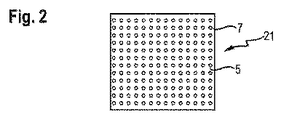
第2のステップにおいて、図2から分かるように、絶縁層5内に複数の孔7が、絶縁層5の行方向及び列方向の両方において1つの孔7から他の孔まで等距離10mmの繰り返しパターンで(レーザーアブレーションによって)形成される。これにより、孔7の一般的な分布が得られる。導電性キャリア基板3はパターニングされた絶縁層5とともに、本発明に係るOLED素子の製造のための基礎として使用することができる、本発明の一実施形態に係る半製品21を構成する。したがって、図3〜7を参照して説明される全ての後続のステップは、半製品21の製造直後に必ずしも実行する必要がないステップとして考えることができる。むしろ、それらはより後の時間、すなわち、少なくとも数日後、場合によっては数週間、数ヶ月、又は1年以上経過した後にさえ実行されてもよい。また、異なる用途のための異なるOLED素子を同じ半製品21をもとにして製造することができる。この文脈において、後述の図面を参照して説明される更なるステップが半製品21の製造に含まれてもよい。これは、図3と関連して説明されるステップに関して最も当てはまる。
In the second step, as can be seen from FIG. 2, a plurality of
ここで、第3のステップにおいて、例えばスクリーン印刷によって絶縁層5の上面10に導電性コーティング9が構築される。これにより、導電性コーティング9の材料が絶縁層5の孔7内にも流れ込み、孔7内に導電性キャリア基板3と導電性コーティング9との間の導電性コンタクト8が形成される。
Here, in a third step, a conductive coating 9 is constructed on the upper surface 10 of the insulating
第4のステップにおいて、導電性コーティング9がフォトリソグラフィック・パターニング処理によってパターニングされる。これにより、ギャップ23によって導電性コーティング9の他の部分から隔てられた複数の個別の第1の電極領域11又はアノード11が得られる。いずれのアノード11も、(導電性コーティング9の下に)複数の孔7が配列された領域を覆う。これは、複数の孔7が下側の導電性キャリア基板3から各アノード11に電流を供給することを意味する。
In the fourth step, the conductive coating 9 is patterned by a photolithographic patterning process. This provides a plurality of individual
図5は、本発明に係る方法の一実施形態における第5のステップの後の半製品21を示す。導電性コーティング9と導電性キャリア基板3との間の導電性コンタクト8の一部が、選択された孔7の領域内の導電性キャリア基板3の位置までの全材料を取り除くことによって除去されている。これにより、チャネル16が得られ、チャネル16は、それらが形成された領域内の孔7よりわずかに大きい直径を有する。チャネル16は、導電性キャリア基板3と導電性コーティング9との間の導電性接続を局所的に排除する。第1の電極領域11の外側の全ての導電性コンタクト8がチャネル16によって除去された場合、第1の電極領域11はギャップによって分離された周辺領域から電気的に絶縁される。図5に示すように、導電性キャリア基板3と導電性コーティング9とに電気的に接触する導電性コンタクト8がまだ残っている場合、下記のように切断線C1、C2、C3に沿って単一のOLED素子を切断するとき、導電性コーティングの少なくとも一部を導電性キャリア基板から電気的に絶縁するために、追加の絶縁ギャップ24を加えなければならない。絶縁ギャップは、例えばギャップ23とともにステップ4において加工されてもよいし、別個のステップにおいて加工されてもよい。図6に示すような第6のステップにおいて、これらのチャネル16がギャップ23及び絶縁ギャップとともに他の絶縁材料17、25によって充填される。この絶縁材料はアノード11を導電性コーティングの他の部分から絶縁し、また、絶縁チャネル16を提供する(図7に結果を示す)。
FIG. 5 shows the
ここで、第7及び後続の第8のステップにおいて、半製品21は本発明の一実施形態に係るOLED素子1に進められている。アノード11の上に、絶縁材料17を有するギャップ23によって縁取られた有機発光層13が形成される。発光層13上には、更に、(左側において)導電性コーティング9を部分的に覆い、(右側において)ギャップ23の絶縁体17まで広がる第2の電極層15又はカソード15が形成される。カソード15が導電性コーティング9と直接接触する領域において、絶縁チャネル16により導電性キャリア基板3への接続は封じられている。この端部領域19は、OLEDデバイス1のカソード15と電気接触するための接触領域として機能する。
Here, in the seventh and subsequent eighth steps, the
再び図5を参照して、複数の切断線C1、C2、C3を確認することができる。これらは、ここで製造されるようなOLED素子のアレイから切り出すことができる単一のOLED素子1の境界を定める。これらの切断線に沿って切断されると、図7に示す種類のOLED素子1を6つ生産できる。 Referring to FIG. 5 again, a plurality of cutting lines C1, C2, and C3 can be confirmed. These delimit a single OLED element 1 that can be cut from an array of OLED elements as manufactured here. When cut along these cutting lines, six OLED elements 1 of the type shown in FIG. 7 can be produced.
本発明は好ましい実施形態及びそれらの変形例の形態で開示されているが、本発明の範囲から逸脱することなく、多数の追加の改変及び変形を施し得ることが理解されるであろう。例えば、本発明に係るOLED素子はより多くの層を含んでもよい。また、OLED素子1をAC源と電気的に接触させるための接触領域は、OLEDの動作に適するアノード(及び導電性キャリア基板)及びカソードのいかなる選択されたスポットに規定されてもよい。 Although the present invention has been disclosed in the form of preferred embodiments and variations thereof, it will be understood that numerous additional modifications and variations may be made without departing from the scope of the invention. For example, the OLED element according to the present invention may include more layers. Also, the contact area for making the OLED element 1 in electrical contact with the AC source may be defined at any selected spot of the anode (and conductive carrier substrate) and cathode suitable for OLED operation.
明確にするために、本願を通じて要素は複数を除外せず、また、「含む(又は備える若しくは有する)」は他のステップ又は要素を除外しない。 For clarity, elements throughout the application do not exclude a plurality, and “include (or include)” does not exclude other steps or elements.
Claims (15)
−b)少なくとも前記第1のキャリア表面の全領域にかけて絶縁材料のパターニングされた層を構築するステップであって、前記絶縁材料の層は、前記第1のキャリア表面の反対側に面する前記絶縁材料の層の上面から前記第1のキャリア表面への電気的アクセスが可能なように複数の孔によってパターニングされる、ステップと、
−c)前記絶縁材料の上面にパターニングされた導電性コーティングを構築するステップであって、前記導電性コーティングは、前記孔に入り込み、前記絶縁材料の全領域を覆い、また、前記導電性コーティング内に複数の個別の第1の電極領域が形成されるようパターニングされる、ステップと、
−d)少なくとも1つの前記第1の電極領域上に有機発光層を形成するステップと、
−e)前記有機発光層上に第2の電極層を形成するステップと
を含む、OLEDの製造方法。 -A) providing a conductive carrier substrate in the form of a metal film or metal foil having a first carrier surface and a second carrier surface;
-B) building a patterned layer of insulating material over at least the entire area of the first carrier surface, the layer of insulating material facing away from the first carrier surface; Patterning with a plurality of holes to allow electrical access from an upper surface of a layer of material to the first carrier surface;
-C) constructing a patterned conductive coating on the top surface of the insulating material, the conductive coating entering the hole, covering the entire area of the insulating material, and within the conductive coating Patterning to form a plurality of individual first electrode regions;
-D) forming an organic light emitting layer on the at least one first electrode region;
And e) forming a second electrode layer on the organic light emitting layer.
−b1)前記絶縁材料の層によって少なくとも前記第1のキャリア表面の全領域をコーティングするステップと、
−b2)前記絶縁材料の層内に前記複数の孔を形成することによって前記絶縁材料の層をパターニングするステップと
を含み、且つ/又は、前記構築ステップc)は、
−c1)前記導電性コーティングが前記孔に入り込み、前記絶縁材料の全領域を覆うよう、前記絶縁材料の上面に前記導電性コーティングを形成するステップと、
−c2)前記複数の個別の第1の電極領域が前記導電性コーティング内に形成されるよう前記導電性コーティングをパターニングするステップと
を含む、請求項1に記載の方法。 The construction step b)
-B1) coating at least the entire area of the first carrier surface with the layer of insulating material;
-B2) patterning the layer of insulating material by forming the plurality of holes in the layer of insulating material, and / or the building step c)
-C1) forming the conductive coating on the top surface of the insulating material so that the conductive coating enters the hole and covers the entire area of the insulating material;
And c2) patterning the conductive coating such that the plurality of individual first electrode regions are formed in the conductive coating.
−a)第1のキャリア表面及び第2のキャリア表面を有する金属フィルム又は金属ホイルの形態の導電性キャリア基板と、
−b)少なくとも前記第1のキャリア表面の全領域上にコーティングされた絶縁材料の層であって、前記絶縁材料の層は、前記第1のキャリア表面の反対側に面する前記絶縁材料の層の上面から前記第1のキャリア表面への電気的アクセスが可能なように複数の孔を含むパターンを有する、絶縁材料の層と、
−c)前記孔内に入り込み、前記絶縁材料の全領域を覆い、また、前記導電性コーティング内に複数の個別の第1の電極領域が形成されるようなパターンを有する、前記絶縁材料の前記上面における導電性コーティングと
を含む、半製品。 A semi-finished product for the production of OLED elements,
-A) a conductive carrier substrate in the form of a metal film or metal foil having a first carrier surface and a second carrier surface;
-B) and at least a layer of the coated insulating material on the entire area of the first surface of the carrier, said layer of insulating material, said layer of insulating material facing away from the first carrier surface A layer of insulating material having a pattern comprising a plurality of holes to allow electrical access from the top surface of the first carrier surface to the first carrier surface;
-C) enters into said bore, said insulating the entire region has covering materials, also has a pattern such as a plurality of individual first electrode region on the conductive inside coating is formed, the insulating material A semi-finished product comprising a conductive coating on said top surface.
−b)少なくとも前記第1のキャリア表面の全領域上にコーティングされた絶縁材料の層であって、前記絶縁材料の層は、前記第1のキャリア表面の反対側に面する前記絶縁材料の層の上面から前記第1のキャリア表面への電気的アクセスが可能なように、複数の孔を含むパターンを有する、絶縁材料の層と、
−c)前記絶縁材料の前記上面における導電性コーティングであって、前記導電性コーティングは前記孔内に入り込み、前記絶縁材料の全領域を覆い、また、前記導電性コーティング内に複数の個別の第1の電極領域が形成されるようなパターンを有する、導電性コーティングと、
−d)少なくとも1つの前記第1の電極領域上の有機発光層と、
−e)前記有機発光層上に形成された第2の電極層と
を含む、OLED素子。 -A) a conductive carrier substrate in the form of a metal film or metal foil having a first carrier surface and a second carrier surface;
-B) a layer of insulating material coated over at least the entire area of the first carrier surface, wherein the layer of insulating material faces the opposite side of the first carrier surface A layer of insulating material having a pattern including a plurality of holes so as to allow electrical access from the top surface of the first carrier surface to the first carrier surface;
-C) a conductive coating on the top surface of the insulating material, wherein the conductive coating penetrates into the hole, covers the entire area of the insulating material, and a plurality of individual second layers within the conductive coating; A conductive coating having a pattern such that one electrode region is formed;
-D) an organic light emitting layer on at least one of the first electrode regions;
-E) OLED element containing the 2nd electrode layer formed on the said organic light emitting layer.
Applications Claiming Priority (3)
| Application Number | Priority Date | Filing Date | Title |
|---|---|---|---|
| US201261594434P | 2012-02-03 | 2012-02-03 | |
| US61/594,434 | 2012-02-03 | ||
| PCT/IB2013/050788 WO2013114295A1 (en) | 2012-02-03 | 2013-01-30 | Oled device and manufacture thereof |
Publications (3)
| Publication Number | Publication Date |
|---|---|
| JP2015505639A JP2015505639A (en) | 2015-02-23 |
| JP2015505639A5 JP2015505639A5 (en) | 2016-03-17 |
| JP6223360B2 true JP6223360B2 (en) | 2017-11-01 |
Family
ID=47915302
Family Applications (1)
| Application Number | Title | Priority Date | Filing Date |
|---|---|---|---|
| JP2014555367A Active JP6223360B2 (en) | 2012-02-03 | 2013-01-30 | OLED element and its manufacture |
Country Status (6)
| Country | Link |
|---|---|
| US (2) | US9543540B2 (en) |
| EP (1) | EP2810314B1 (en) |
| JP (1) | JP6223360B2 (en) |
| CN (1) | CN104094431B (en) |
| RU (1) | RU2626996C2 (en) |
| WO (1) | WO2013114295A1 (en) |
Families Citing this family (9)
| Publication number | Priority date | Publication date | Assignee | Title |
|---|---|---|---|---|
| EP3053204B1 (en) | 2013-10-03 | 2023-03-29 | OLEDWorks GmbH | Voltage-light conversion device |
| KR20150102180A (en) | 2014-02-27 | 2015-09-07 | 삼성디스플레이 주식회사 | Laser beam irradiation apparatus and manufacturing method of organic light emitting display apparatus using the same |
| DE102014110052B4 (en) * | 2014-07-17 | 2020-04-16 | Osram Oled Gmbh | Optoelectronic component and method for producing an optoelectronic component |
| DE102014112171B4 (en) | 2014-08-26 | 2018-01-25 | Osram Oled Gmbh | Method for detecting a short circuit in a first light emitting diode element and optoelectronic assembly |
| KR102460417B1 (en) | 2014-10-24 | 2022-10-31 | 코닝 인코포레이티드 | Oleds with improved light extraction using enhanced guided mode coupling |
| DE102015100099B4 (en) * | 2015-01-07 | 2017-10-19 | Osram Oled Gmbh | Method for producing an organic light-emitting component |
| CN109075265A (en) | 2016-04-05 | 2018-12-21 | 康宁公司 | Patterning Organic Light Emitting Diode (OLED) with enhancing light extraction |
| US11318458B2 (en) | 2017-04-03 | 2022-05-03 | Hewlett-Packard Development Company, L.P. | Cassette substrates made of polyetherimide |
| TWI718630B (en) * | 2019-08-20 | 2021-02-11 | 和碩聯合科技股份有限公司 | Light emitting device |
Family Cites Families (23)
| Publication number | Priority date | Publication date | Assignee | Title |
|---|---|---|---|---|
| JP4626018B2 (en) * | 2000-06-30 | 2011-02-02 | ソニー株式会社 | Organic electroluminescence display device |
| KR100484591B1 (en) * | 2001-12-29 | 2005-04-20 | 엘지.필립스 엘시디 주식회사 | an active matrix organic electroluminescence display and a manufacturing method of the same |
| JP3942017B2 (en) * | 2002-03-25 | 2007-07-11 | 富士フイルム株式会社 | Light emitting element |
| TWI255432B (en) * | 2002-06-03 | 2006-05-21 | Lg Philips Lcd Co Ltd | Active matrix organic electroluminescent display device and fabricating method thereof |
| US6642092B1 (en) | 2002-07-11 | 2003-11-04 | Sharp Laboratories Of America, Inc. | Thin-film transistors formed on a metal foil substrate |
| JP3994994B2 (en) * | 2003-10-23 | 2007-10-24 | セイコーエプソン株式会社 | Organic EL device manufacturing method, organic EL device, and electronic apparatus |
| EP1712109A4 (en) * | 2003-12-30 | 2008-03-19 | Agency Science Tech & Res | Flexible electroluminescent devices |
| KR100625999B1 (en) * | 2004-02-26 | 2006-09-20 | 삼성에스디아이 주식회사 | Donor sheet, manufacturing method of the donor sheet, manufacturing method of TFT using the donor sheet, and manufacturing method of flat panel display using the donor sheet |
| US20070077349A1 (en) * | 2005-09-30 | 2007-04-05 | Eastman Kodak Company | Patterning OLED device electrodes and optical material |
| RU2414018C2 (en) * | 2005-12-19 | 2011-03-10 | Конинклейке Филипс Электроникс Н.В. | Organic electroluminescent device |
| WO2008068293A1 (en) | 2006-12-07 | 2008-06-12 | Thomson Licensing | Panel of organic light-emitting diodes, provided with integrated top supply electrodes |
| JP5006108B2 (en) * | 2007-06-01 | 2012-08-22 | 株式会社ジャパンディスプレイイースト | Display device |
| JP5260647B2 (en) * | 2007-07-11 | 2013-08-14 | コーニンクレッカ フィリップス エレクトロニクス エヌ ヴィ | Organic functional element and method for producing the element |
| TW201001776A (en) * | 2008-02-22 | 2010-01-01 | Koninkl Philips Electronics Nv | Double sided organic light emitting diode (OLED) |
| JP2011517081A (en) * | 2008-04-02 | 2011-05-26 | コーニンクレッカ フィリップス エレクトロニクス エヌ ヴィ | Light emitting diode device |
| KR100982412B1 (en) * | 2008-05-29 | 2010-09-15 | (주)에이디에스 | Electro-optic device and mthod for manufacturing the same |
| JP5142846B2 (en) * | 2008-06-17 | 2013-02-13 | 株式会社日立製作所 | Organic light emitting device |
| CN102172101B (en) * | 2008-10-06 | 2015-07-08 | 旭硝子株式会社 | Substrate for electronic device, method for producing same, electronic device using same, method for producing same and substrate for organic led element |
| US8013525B2 (en) | 2009-04-09 | 2011-09-06 | Global Oled Technology Llc | Flexible OLED display with chiplets |
| EP2513999A1 (en) * | 2009-12-16 | 2012-10-24 | Koninklijke Philips Electronics N.V. | Method for creating serial connected oled-devices |
| EP2363905A1 (en) * | 2010-03-05 | 2011-09-07 | Nederlandse Organisatie voor toegepast -natuurwetenschappelijk onderzoek TNO | Opto-electrical device and method for manufacturing thereof |
| US8618731B2 (en) | 2010-05-18 | 2013-12-31 | General Electric Company | Large-area flexible OLED light source |
| KR101408463B1 (en) | 2010-09-01 | 2014-06-17 | 쇼와 덴코 가부시키가이샤 | Electroluminescent element, display device and lighting device |
-
2013
- 2013-01-30 JP JP2014555367A patent/JP6223360B2/en active Active
- 2013-01-30 WO PCT/IB2013/050788 patent/WO2013114295A1/en active Application Filing
- 2013-01-30 EP EP13711474.0A patent/EP2810314B1/en active Active
- 2013-01-30 RU RU2014135770A patent/RU2626996C2/en active
- 2013-01-30 US US14/375,279 patent/US9543540B2/en active Active
- 2013-01-30 CN CN201380007689.4A patent/CN104094431B/en active Active
-
2016
- 2016-11-18 US US15/355,174 patent/US9755185B2/en active Active
Also Published As
| Publication number | Publication date |
|---|---|
| EP2810314A1 (en) | 2014-12-10 |
| CN104094431B (en) | 2018-03-27 |
| US9543540B2 (en) | 2017-01-10 |
| CN104094431A (en) | 2014-10-08 |
| EP2810314B1 (en) | 2020-08-12 |
| WO2013114295A1 (en) | 2013-08-08 |
| RU2626996C2 (en) | 2017-08-02 |
| RU2014135770A (en) | 2016-03-27 |
| US20150008415A1 (en) | 2015-01-08 |
| US20170069875A1 (en) | 2017-03-09 |
| US9755185B2 (en) | 2017-09-05 |
| JP2015505639A (en) | 2015-02-23 |
Similar Documents
| Publication | Publication Date | Title |
|---|---|---|
| JP6223360B2 (en) | OLED element and its manufacture | |
| EP2483944B1 (en) | Process for fabricating a monolithic parallel interconnect structure of an optoelectronic device | |
| US9680123B2 (en) | Light emitting device, electrode structure and manufacturing method thereof | |
| US20110186905A1 (en) | Oled device with covered shunt line | |
| US8692457B2 (en) | Large area light emitting electrical package with current spreading bus | |
| JP2015505639A5 (en) | ||
| TWI517746B (en) | Electroluminescent device | |
| JP5396036B2 (en) | Organic EL device | |
| US20120295372A1 (en) | Method of maskless manufacturing of oled devices | |
| JP2013514621A (en) | Method for producing series-connected OLED devices | |
| US10141535B2 (en) | Optoelectronic component and a method for producing an optoelectronic component | |
| US20170301874A1 (en) | Organic el panel and method for producing same | |
| JP6163334B2 (en) | Organic EL device | |
| KR102174809B1 (en) | Voltage-light conversion device | |
| JP6190606B2 (en) | Organic EL device and method for manufacturing organic EL device | |
| KR101032950B1 (en) | Method for manufacturing organic electroluminescence device | |
| JP2017162765A (en) | Light-emitting device | |
| JP2014203527A (en) | Joining structure and light-emitting device |
Legal Events
| Date | Code | Title | Description |
|---|---|---|---|
| A521 | Request for written amendment filed |
Free format text: JAPANESE INTERMEDIATE CODE: A523 Effective date: 20160128 |
|
| A621 | Written request for application examination |
Free format text: JAPANESE INTERMEDIATE CODE: A621 Effective date: 20160128 |
|
| A977 | Report on retrieval |
Free format text: JAPANESE INTERMEDIATE CODE: A971007 Effective date: 20161020 |
|
| A131 | Notification of reasons for refusal |
Free format text: JAPANESE INTERMEDIATE CODE: A131 Effective date: 20161206 |
|
| A521 | Request for written amendment filed |
Free format text: JAPANESE INTERMEDIATE CODE: A523 Effective date: 20170301 |
|
| TRDD | Decision of grant or rejection written | ||
| A01 | Written decision to grant a patent or to grant a registration (utility model) |
Free format text: JAPANESE INTERMEDIATE CODE: A01 Effective date: 20170904 |
|
| A61 | First payment of annual fees (during grant procedure) |
Free format text: JAPANESE INTERMEDIATE CODE: A61 Effective date: 20171003 |
|
| R150 | Certificate of patent or registration of utility model |
Ref document number: 6223360 Country of ref document: JP Free format text: JAPANESE INTERMEDIATE CODE: R150 |
|
| R250 | Receipt of annual fees |
Free format text: JAPANESE INTERMEDIATE CODE: R250 |
|
| R250 | Receipt of annual fees |
Free format text: JAPANESE INTERMEDIATE CODE: R250 |
|
| R250 | Receipt of annual fees |
Free format text: JAPANESE INTERMEDIATE CODE: R250 |
|
| R250 | Receipt of annual fees |
Free format text: JAPANESE INTERMEDIATE CODE: R250 |