JP2012503338A - CVD reactor having a plurality of processing levels and a biaxial motor lift mechanism - Google Patents
CVD reactor having a plurality of processing levels and a biaxial motor lift mechanism Download PDFInfo
- Publication number
- JP2012503338A JP2012503338A JP2011527949A JP2011527949A JP2012503338A JP 2012503338 A JP2012503338 A JP 2012503338A JP 2011527949 A JP2011527949 A JP 2011527949A JP 2011527949 A JP2011527949 A JP 2011527949A JP 2012503338 A JP2012503338 A JP 2012503338A
- Authority
- JP
- Japan
- Prior art keywords
- substrate
- processing
- lift
- substrate support
- support
- Prior art date
- Legal status (The legal status is an assumption and is not a legal conclusion. Google has not performed a legal analysis and makes no representation as to the accuracy of the status listed.)
- Pending
Links
- 230000007246 mechanism Effects 0.000 title abstract description 12
- 239000000758 substrate Substances 0.000 claims abstract description 173
- 238000000034 method Methods 0.000 claims abstract description 61
- 230000008569 process Effects 0.000 claims abstract description 51
- 239000004065 semiconductor Substances 0.000 claims description 9
- 238000005192 partition Methods 0.000 claims description 6
- 230000033001 locomotion Effects 0.000 abstract description 11
- 230000000737 periodic effect Effects 0.000 abstract description 2
- 238000010924 continuous production Methods 0.000 abstract 1
- 238000009434 installation Methods 0.000 abstract 1
- 239000007789 gas Substances 0.000 description 47
- 238000000151 deposition Methods 0.000 description 21
- 230000008878 coupling Effects 0.000 description 19
- 238000010168 coupling process Methods 0.000 description 19
- 238000005859 coupling reaction Methods 0.000 description 19
- 230000008021 deposition Effects 0.000 description 17
- 239000010453 quartz Substances 0.000 description 16
- VYPSYNLAJGMNEJ-UHFFFAOYSA-N silicon dioxide Inorganic materials O=[Si]=O VYPSYNLAJGMNEJ-UHFFFAOYSA-N 0.000 description 16
- 239000002243 precursor Substances 0.000 description 10
- XUIMIQQOPSSXEZ-UHFFFAOYSA-N Silicon Chemical compound [Si] XUIMIQQOPSSXEZ-UHFFFAOYSA-N 0.000 description 8
- 229910052710 silicon Inorganic materials 0.000 description 8
- 239000010703 silicon Substances 0.000 description 8
- 238000006243 chemical reaction Methods 0.000 description 7
- 238000009826 distribution Methods 0.000 description 7
- 239000000463 material Substances 0.000 description 7
- 230000006835 compression Effects 0.000 description 5
- 238000007906 compression Methods 0.000 description 5
- 230000005855 radiation Effects 0.000 description 5
- 229910000577 Silicon-germanium Inorganic materials 0.000 description 4
- LEVVHYCKPQWKOP-UHFFFAOYSA-N [Si].[Ge] Chemical compound [Si].[Ge] LEVVHYCKPQWKOP-UHFFFAOYSA-N 0.000 description 4
- 238000013459 approach Methods 0.000 description 4
- 238000000407 epitaxy Methods 0.000 description 4
- 239000006227 byproduct Substances 0.000 description 3
- 238000005137 deposition process Methods 0.000 description 3
- 238000004519 manufacturing process Methods 0.000 description 3
- 238000010926 purge Methods 0.000 description 3
- 239000000376 reactant Substances 0.000 description 3
- 238000004140 cleaning Methods 0.000 description 2
- 239000000112 cooling gas Substances 0.000 description 2
- 238000010586 diagram Methods 0.000 description 2
- 229910052732 germanium Inorganic materials 0.000 description 2
- GNPVGFCGXDBREM-UHFFFAOYSA-N germanium atom Chemical compound [Ge] GNPVGFCGXDBREM-UHFFFAOYSA-N 0.000 description 2
- 238000010438 heat treatment Methods 0.000 description 2
- 238000011068 loading method Methods 0.000 description 2
- 229910044991 metal oxide Inorganic materials 0.000 description 2
- 150000004706 metal oxides Chemical class 0.000 description 2
- 230000004044 response Effects 0.000 description 2
- HBMJWWWQQXIZIP-UHFFFAOYSA-N silicon carbide Chemical compound [Si+]#[C-] HBMJWWWQQXIZIP-UHFFFAOYSA-N 0.000 description 2
- 229910010271 silicon carbide Inorganic materials 0.000 description 2
- 239000002210 silicon-based material Substances 0.000 description 2
- 229910001220 stainless steel Inorganic materials 0.000 description 2
- 239000010935 stainless steel Substances 0.000 description 2
- ZOXJGFHDIHLPTG-UHFFFAOYSA-N Boron Chemical compound [B] ZOXJGFHDIHLPTG-UHFFFAOYSA-N 0.000 description 1
- 230000004913 activation Effects 0.000 description 1
- 229910052782 aluminium Inorganic materials 0.000 description 1
- XAGFODPZIPBFFR-UHFFFAOYSA-N aluminium Chemical compound [Al] XAGFODPZIPBFFR-UHFFFAOYSA-N 0.000 description 1
- 238000000137 annealing Methods 0.000 description 1
- 230000003466 anti-cipated effect Effects 0.000 description 1
- 230000004888 barrier function Effects 0.000 description 1
- 230000008901 benefit Effects 0.000 description 1
- 229910052796 boron Inorganic materials 0.000 description 1
- 229910010293 ceramic material Inorganic materials 0.000 description 1
- 238000005229 chemical vapour deposition Methods 0.000 description 1
- 238000004891 communication Methods 0.000 description 1
- 230000000295 complement effect Effects 0.000 description 1
- 238000011109 contamination Methods 0.000 description 1
- 238000001816 cooling Methods 0.000 description 1
- 230000001419 dependent effect Effects 0.000 description 1
- 238000003795 desorption Methods 0.000 description 1
- 230000001066 destructive effect Effects 0.000 description 1
- 239000003085 diluting agent Substances 0.000 description 1
- 239000002019 doping agent Substances 0.000 description 1
- 238000005530 etching Methods 0.000 description 1
- 230000005669 field effect Effects 0.000 description 1
- 239000007770 graphite material Substances 0.000 description 1
- 239000007943 implant Substances 0.000 description 1
- 230000006872 improvement Effects 0.000 description 1
- 238000011065 in-situ storage Methods 0.000 description 1
- 230000006698 induction Effects 0.000 description 1
- 230000001939 inductive effect Effects 0.000 description 1
- 238000009616 inductively coupled plasma Methods 0.000 description 1
- 239000012212 insulator Substances 0.000 description 1
- 239000000203 mixture Substances 0.000 description 1
- 230000005693 optoelectronics Effects 0.000 description 1
- 229920000642 polymer Polymers 0.000 description 1
- 238000002360 preparation method Methods 0.000 description 1
- 239000012495 reaction gas Substances 0.000 description 1
- 229910021332 silicide Inorganic materials 0.000 description 1
- FVBUAEGBCNSCDD-UHFFFAOYSA-N silicide(4-) Chemical compound [Si-4] FVBUAEGBCNSCDD-UHFFFAOYSA-N 0.000 description 1
- 238000001179 sorption measurement Methods 0.000 description 1
- 238000006557 surface reaction Methods 0.000 description 1
Images
Classifications
-
- H—ELECTRICITY
- H01—ELECTRIC ELEMENTS
- H01L—SEMICONDUCTOR DEVICES NOT COVERED BY CLASS H10
- H01L21/00—Processes or apparatus adapted for the manufacture or treatment of semiconductor or solid state devices or of parts thereof
- H01L21/67—Apparatus specially adapted for handling semiconductor or electric solid state devices during manufacture or treatment thereof; Apparatus specially adapted for handling wafers during manufacture or treatment of semiconductor or electric solid state devices or components ; Apparatus not specifically provided for elsewhere
- H01L21/67005—Apparatus not specifically provided for elsewhere
- H01L21/67011—Apparatus for manufacture or treatment
- H01L21/67098—Apparatus for thermal treatment
- H01L21/67115—Apparatus for thermal treatment mainly by radiation
-
- C—CHEMISTRY; METALLURGY
- C23—COATING METALLIC MATERIAL; COATING MATERIAL WITH METALLIC MATERIAL; CHEMICAL SURFACE TREATMENT; DIFFUSION TREATMENT OF METALLIC MATERIAL; COATING BY VACUUM EVAPORATION, BY SPUTTERING, BY ION IMPLANTATION OR BY CHEMICAL VAPOUR DEPOSITION, IN GENERAL; INHIBITING CORROSION OF METALLIC MATERIAL OR INCRUSTATION IN GENERAL
- C23C—COATING METALLIC MATERIAL; COATING MATERIAL WITH METALLIC MATERIAL; SURFACE TREATMENT OF METALLIC MATERIAL BY DIFFUSION INTO THE SURFACE, BY CHEMICAL CONVERSION OR SUBSTITUTION; COATING BY VACUUM EVAPORATION, BY SPUTTERING, BY ION IMPLANTATION OR BY CHEMICAL VAPOUR DEPOSITION, IN GENERAL
- C23C16/00—Chemical coating by decomposition of gaseous compounds, without leaving reaction products of surface material in the coating, i.e. chemical vapour deposition [CVD] processes
- C23C16/44—Chemical coating by decomposition of gaseous compounds, without leaving reaction products of surface material in the coating, i.e. chemical vapour deposition [CVD] processes characterised by the method of coating
- C23C16/455—Chemical coating by decomposition of gaseous compounds, without leaving reaction products of surface material in the coating, i.e. chemical vapour deposition [CVD] processes characterised by the method of coating characterised by the method used for introducing gases into reaction chamber or for modifying gas flows in reaction chamber
- C23C16/45523—Pulsed gas flow or change of composition over time
- C23C16/45525—Atomic layer deposition [ALD]
- C23C16/45544—Atomic layer deposition [ALD] characterized by the apparatus
- C23C16/45548—Atomic layer deposition [ALD] characterized by the apparatus having arrangements for gas injection at different locations of the reactor for each ALD half-reaction
- C23C16/45551—Atomic layer deposition [ALD] characterized by the apparatus having arrangements for gas injection at different locations of the reactor for each ALD half-reaction for relative movement of the substrate and the gas injectors or half-reaction reactor compartments
-
- H—ELECTRICITY
- H01—ELECTRIC ELEMENTS
- H01L—SEMICONDUCTOR DEVICES NOT COVERED BY CLASS H10
- H01L21/00—Processes or apparatus adapted for the manufacture or treatment of semiconductor or solid state devices or of parts thereof
- H01L21/67—Apparatus specially adapted for handling semiconductor or electric solid state devices during manufacture or treatment thereof; Apparatus specially adapted for handling wafers during manufacture or treatment of semiconductor or electric solid state devices or components ; Apparatus not specifically provided for elsewhere
- H01L21/683—Apparatus specially adapted for handling semiconductor or electric solid state devices during manufacture or treatment thereof; Apparatus specially adapted for handling wafers during manufacture or treatment of semiconductor or electric solid state devices or components ; Apparatus not specifically provided for elsewhere for supporting or gripping
- H01L21/687—Apparatus specially adapted for handling semiconductor or electric solid state devices during manufacture or treatment thereof; Apparatus specially adapted for handling wafers during manufacture or treatment of semiconductor or electric solid state devices or components ; Apparatus not specifically provided for elsewhere for supporting or gripping using mechanical means, e.g. chucks, clamps or pinches
- H01L21/68714—Apparatus specially adapted for handling semiconductor or electric solid state devices during manufacture or treatment thereof; Apparatus specially adapted for handling wafers during manufacture or treatment of semiconductor or electric solid state devices or components ; Apparatus not specifically provided for elsewhere for supporting or gripping using mechanical means, e.g. chucks, clamps or pinches the wafers being placed on a susceptor, stage or support
- H01L21/68742—Apparatus specially adapted for handling semiconductor or electric solid state devices during manufacture or treatment thereof; Apparatus specially adapted for handling wafers during manufacture or treatment of semiconductor or electric solid state devices or components ; Apparatus not specifically provided for elsewhere for supporting or gripping using mechanical means, e.g. chucks, clamps or pinches the wafers being placed on a susceptor, stage or support characterised by a lifting arrangement, e.g. lift pins
-
- H—ELECTRICITY
- H01—ELECTRIC ELEMENTS
- H01L—SEMICONDUCTOR DEVICES NOT COVERED BY CLASS H10
- H01L21/00—Processes or apparatus adapted for the manufacture or treatment of semiconductor or solid state devices or of parts thereof
- H01L21/67—Apparatus specially adapted for handling semiconductor or electric solid state devices during manufacture or treatment thereof; Apparatus specially adapted for handling wafers during manufacture or treatment of semiconductor or electric solid state devices or components ; Apparatus not specifically provided for elsewhere
- H01L21/683—Apparatus specially adapted for handling semiconductor or electric solid state devices during manufacture or treatment thereof; Apparatus specially adapted for handling wafers during manufacture or treatment of semiconductor or electric solid state devices or components ; Apparatus not specifically provided for elsewhere for supporting or gripping
- H01L21/687—Apparatus specially adapted for handling semiconductor or electric solid state devices during manufacture or treatment thereof; Apparatus specially adapted for handling wafers during manufacture or treatment of semiconductor or electric solid state devices or components ; Apparatus not specifically provided for elsewhere for supporting or gripping using mechanical means, e.g. chucks, clamps or pinches
- H01L21/68714—Apparatus specially adapted for handling semiconductor or electric solid state devices during manufacture or treatment thereof; Apparatus specially adapted for handling wafers during manufacture or treatment of semiconductor or electric solid state devices or components ; Apparatus not specifically provided for elsewhere for supporting or gripping using mechanical means, e.g. chucks, clamps or pinches the wafers being placed on a susceptor, stage or support
- H01L21/68792—Apparatus specially adapted for handling semiconductor or electric solid state devices during manufacture or treatment thereof; Apparatus specially adapted for handling wafers during manufacture or treatment of semiconductor or electric solid state devices or components ; Apparatus not specifically provided for elsewhere for supporting or gripping using mechanical means, e.g. chucks, clamps or pinches the wafers being placed on a susceptor, stage or support characterised by the construction of the shaft
Abstract
基板を処理するための装置は、プロセシングチャンバならびにチャンバ内に配置された基板支持部およびリフトピンアセンブリを備える。基板支持部およびリフトピンを設置することを制御し、基板支持部の回転を与えるリフト機構に、基板支持部およびリフトピンアセンブリを連結する。リフト機構は、基板支持部とリフトピンとの間のクリアランスが基板支持部の回転を始めることを許容するときに信号を発生することが可能な少なくとも1つのセンサを含む。同時の軸方向の動作および回転が可能な基板支持部を、端部リングによって分離された複数のプロセシングゾーンを備えるプロセシングチャンバ内で使用することができる。基板は、複数のプロセシングゾーン間を動かすことによって連続するプロセスまたは周期的なプロセスを受けることができる。 An apparatus for processing a substrate includes a processing chamber and a substrate support and lift pin assembly disposed within the chamber. The substrate support and the lift pin assembly are coupled to a lift mechanism that controls the installation of the substrate support and the lift pins and provides rotation of the substrate support. The lift mechanism includes at least one sensor capable of generating a signal when the clearance between the substrate support and the lift pins allows the substrate support to begin rotating. A substrate support capable of simultaneous axial movement and rotation can be used in a processing chamber comprising a plurality of processing zones separated by end rings. The substrate may be subjected to a continuous process or a periodic process by moving between multiple processing zones.
Description
本発明の実施形態は、エピタキシャル堆積プロセスまたは他の化学気相堆積プロセスなどの、半導体基板上の堆積反応およびエッチ反応に関する。より詳しくは、本発明の実施形態は、かかるプロセスを実行するために基板を巧みに操作するための装置に関する。 Embodiments of the present invention relate to deposition and etch reactions on semiconductor substrates, such as epitaxial deposition processes or other chemical vapor deposition processes. More particularly, embodiments of the present invention relate to an apparatus for manipulating a substrate to perform such a process.
シリコン膜および/またはゲルマニウム含有膜のエピタキシャル成長は、多くのデバイスの中で特に、先端ロジックデバイスおよびDRAMデバイスに対する新たな応用のために重要性が増してきている。より小さなトランジスタが製造されるに従って、シリコン含有MOSFET(金属酸化物半導体電界効果型トランジスタ)デバイスなどの、サブ100nmCMOS(相補型金属酸化物半導体)デバイス用の超シャローソース/ドレイン接合は、作製することがさらに困難になってきている。シリコン系材料を、MOSFETデバイス用のデバイス製作の際に使用することができる。例えば、PMOS応用例では、トランジスタのリセスした領域中の膜は、通常シリコン−ゲルマニウムであり、NMOS応用例に対しては、リセスした領域中の膜をSiCとすることができる。接合抵抗を減少させるためにシリコン単独よりもより多くのボロンを注入するために、シリコン−ゲルマニウムを有利に使用することができ、これはデバイス性能を改善する、例えば、基板表面のところにシリサイド層のあるシリコン−ゲルマニウム界面は、シリコン−ゲルマニウムとシリコン界面よりも低いショットキーバリアを有する。 Epitaxial growth of silicon and / or germanium-containing films is becoming increasingly important for new applications, especially for advanced logic devices and DRAM devices, among many devices. As smaller transistors are fabricated, ultra-shallow source / drain junctions for sub-100 nm CMOS (complementary metal oxide semiconductor) devices, such as silicon-containing MOSFET (metal oxide semiconductor field effect transistor) devices, must be created. Has become even more difficult. Silicon-based materials can be used in device fabrication for MOSFET devices. For example, in a PMOS application, the film in the recessed region of the transistor is typically silicon-germanium, and for an NMOS application, the film in the recessed region can be SiC. Silicon-germanium can be advantageously used to implant more boron than silicon alone to reduce junction resistance, which improves device performance, for example, a silicide layer at the substrate surface Some silicon-germanium interfaces have a lower Schottky barrier than silicon-germanium and silicon interfaces.
選択的なシリコン−エピタキシャル(Si−エピタキシャル)堆積およびシリコン−ゲルマニウム−エピタキシャル堆積は、絶縁体領域上に何も成長させずにシリコン(Si)モート上にエピ層の成長を可能にする。ソース/ドレイン内や、ソース/ドレインエクステンション内や、コンタクトプラグ内や、バイポーラデバイスのベース層堆積物内など、半導体デバイスにおいて、選択エピタキシを使用することができる。それに加えて、選択エピタキシは、その場ドーピングによるほぼ完全なドーパントの活性化を可能にし、その結果、ポストアニーリングプロセスを省略することができる。それゆえ、シリコンエッチングおよび選択エピタキシによって、接合深さを正確に定めることができる。接合深さの改善は、やはり、圧縮応力を生成する。デバイス製作の際のシリコン含有材料の使用の一例は、MOSFETデバイス用である。 Selective silicon-epitaxial (Si-epitaxial) deposition and silicon-germanium-epitaxial deposition allow the growth of an epi layer on a silicon (Si) mote without growing anything on the insulator region. Selective epitaxy can be used in semiconductor devices, such as in a source / drain, in a source / drain extension, in a contact plug, or in a base layer deposit of a bipolar device. In addition, selective epitaxy allows almost complete dopant activation by in-situ doping, so that the post-annealing process can be omitted. Therefore, the junction depth can be accurately determined by silicon etching and selective epitaxy. The improvement in the joint depth still generates compressive stress. One example of the use of silicon-containing materials in device fabrication is for MOSFET devices.
大部分のプロセスにおけるように、エピタキシャルプロセスの際に基板の効率的で非破壊の巧みな操作が望まれる。例えば、多くのエピタキシャルプロセスでは、一様な堆積を確実にするために基板を回転させる。それに加えて、処理のための準備の際に、およびやはり処理後に、基板を、一般に上昇させたり下降させたりする。基板のハンドリングが、プロセシングチャンバ内に微粒子を発生させることがあるため、かかるハンドリングを比較的穏やかにすることが望まれている。処理中に基板設置の制御は、やはり堆積する膜の品質に影響を与えることがある。従って、最も望まれるように基板を設置し、微粒子を発生させずに基板をハンドリングしつつ、基板上にエピタキシャル膜を堆積させることが可能な装置に対する必要性がある。 As in most processes, efficient and non-destructive manipulation of the substrate during the epitaxial process is desired. For example, in many epitaxial processes, the substrate is rotated to ensure uniform deposition. In addition, the substrate is generally raised or lowered during preparation for processing and also after processing. Since substrate handling can generate particulates in the processing chamber, it is desirable to make such handling relatively gentle. Control of substrate placement during processing can also affect the quality of the deposited film. Accordingly, there is a need for an apparatus capable of depositing an epitaxial film on a substrate while placing the substrate as most desired and handling the substrate without generating particulates.
本発明の実施形態は、一般に、蓋や、フロアや、壁を備えたプロセシングチャンバと、プロセシングチャンバ内に配置され、フロアを貫通するリフトシャフトを有する基板支持部と、チャンバ内で垂直に基板を移動させ、基板支持部の上方に基板を持ち上げるようにリフトピンを動作させ、チャンバ内で基板を移動させながら基板を回転させるように構成されたリフト機構とを備える、基板を処理するための装置を提供する。ある実施形態は、回転を与えるためのモータに連結された磁気アクチュエータを具備し、リフトシャフトに取り付けられた磁気的にアクチュエートされるロータを取り上げる。 Embodiments of the present invention generally include a processing chamber with a lid, a floor, and walls, a substrate support disposed within the processing chamber and having a lift shaft passing through the floor, and a substrate vertically in the chamber. An apparatus for processing a substrate, comprising: a lift mechanism configured to move and operate lift pins to lift the substrate above the substrate support and to rotate the substrate while moving the substrate within the chamber. provide. One embodiment picks up a magnetically actuated rotor that includes a magnetic actuator coupled to a motor for providing rotation and is attached to a lift shaft.
他の実施形態は、プロセスチャンバの内部体積を画定する側壁や上面や底面と、側壁に沿って配置された複数の端部リングであって、各端部リングがプロセスチャンバの内部体積内で少なくとも1つのプロセシングゾーンの境界を画定する、複数の端部リングと、チャンバの内部体積内に配置され、基板支持部の中心軸に平行な方向に動かしながら中心軸の周りを回転させるように構成された基板支持部と、プロセシングチャンバの各プロセシングゾーンに連結されたガス導管とを備える、半導体基板を処理するためのプロセスチャンバを提供する。 Other embodiments include sidewalls, top and bottom surfaces defining an interior volume of the process chamber, and a plurality of end rings disposed along the sidewalls, wherein each end ring is at least within the interior volume of the process chamber. A plurality of end rings that define the boundaries of one processing zone and are disposed within the interior volume of the chamber and are configured to rotate about a central axis while moving in a direction parallel to the central axis of the substrate support. A process chamber for processing a semiconductor substrate is provided that includes a substrate support and a gas conduit coupled to each processing zone of the processing chamber.
他の実施形態は、プロセシングチャンバ内の基板支持部上に基板を設置するステップと、基板支持部上の基板を回転させるステップと、基板を回転させながら回転の軸に沿って基板を動かすステップとを備える、半導体基板を処理する方法を提供する。 Other embodiments include placing a substrate on a substrate support in a processing chamber, rotating the substrate on the substrate support, and moving the substrate along an axis of rotation while rotating the substrate. A method for processing a semiconductor substrate is provided.
従って、本発明の上に記述した特徴を詳細に理解することが可能な方式で、上記に簡潔に要約されている本発明のより明細な説明を、その一部が添付した図面に図示されている実施形態を参照することによって知ることができる。しかしながら、添付した図面が本発明の典型的な実施形態だけを図示し、それゆえ、本発明に関して他の同様に有効な実施形態を許容することができる本発明の範囲を限定するようには見なされないことに、留意すべきである。 Accordingly, a more detailed description of the invention, briefly summarized above, may be found in part in the accompanying drawings, in a manner that provides a thorough understanding of the features described above. By referring to certain embodiments. However, the accompanying drawings illustrate only typical embodiments of the invention and are therefore viewed as limiting the scope of the invention which may allow other equally effective embodiments with respect to the invention. It should be noted that this is not done.
理解を容易にするために、可能である場合には、複数の図に共通な同一の要素を示すために、同一の参照番号を使用している。一実施形態において開示した要素を、具体的な記述がなくとも他の実施形態において利益をもたらすように利用することができることが予想される。 To facilitate understanding, identical reference numerals have been used, where possible, to designate identical elements that are common to the figures. It is anticipated that elements disclosed in one embodiment can be utilized to benefit in other embodiments without specific description.
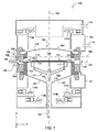
本発明の実施形態は、一般に、基板上に膜を堆積させるための装置を提供する。図1は、エピタキシャル堆積のために構成された堆積チャンバ100の概略的断面図であり、Santa Clara、CaliforniaのApplied Materials,Inc.から入手可能なCENTURA(登録商標)統合プロセシングシステムの一部であり得る。堆積チャンバ100は、アルミニウムまたはステンレス鋼、例えば、316Lステンレス鋼などの、プロセスに耐性のある材料から作られる収納構造物101を含む。収納構造物101は、上部チャンバ105および下部チャンバ124を含み、プロセシング体積118を中に含有する石英チャンバ130などの、プロセスチャンバ100の様々な機能要素を納める。反応種を、ガス分配アセンブリ150によって石英チャンバ130に供給し、真空源(図示せず)と典型的には連通している排出口138によって、プロセシング副生成物をプロセシング体積118から除去する。
Embodiments of the present invention generally provide an apparatus for depositing a film on a substrate. FIG. 1 is a schematic cross-sectional view of a
基板支持部117の表面116上のプロセシング体積118へと移送される基板114を受け取るように、基板支持部117を適合させる。基板支持部117を、セラミック材料または炭化シリコンなどのシリコン材料もしくは他のプロセスに耐性のある材料でコーティングしたグラファイト材料から作ることができる。前駆体反応性物質からの反応種を、基板114の露出した表面に与え、副生成物を基板114の表面からその後で除去することができる。基板114および/またはプロセシング体積118を加熱することを、上部ランプモジュール110Aおよび下部ランプモジュール110Bなどの放射光源によって行うことができる。基板支持部117を、支持シャフト140の移動によって中心軸102に平行な方向に動かしつつ、基板支持部の中心軸102の周りを回転させることができる。基板支持部117の表面116を貫通し、プロセシングチャンバ内への搬送およびチャンバから外への搬送のために基板支持部117の上方に基板114を持ち上げるリフトピン170が設けられる。リフトピン170は、リフトピンカラー174によって支持シャフト140に連結される。
The
一実施形態では、上部ランプモジュール110Aおよび下部ランプモジュール110Bは、赤外線(IR)ランプである。非熱エネルギーまたはランプモジュール110Aおよび110Bからの放射光は、上部石英チャンバ105の上部石英窓104を通り、下部石英チャンバ124の下部石英部分103を通り進む。上部石英チャンバ105用の冷却ガスは、必要であれば、注入口112を介して入り、排出口113を介して出る。前駆体反応性物質および、希釈ガスや、チャンバ100用のパージガスや、ベントガスは、ガス分配アセンブリ150を介して入り、排出口138を介して出る。
In one embodiment, the
反応種を活性化させ、反応物の吸着および基板114の表面116からのプロセス副生成物の脱着を助けるために使用するプロセシング体積118中への短波長放射光は、例えば、エピタキシャル成長させようとする膜の組成に応じて、与えるべき様々な波長と組み合わせて、典型的には約0.8μmから約1.2μmの範囲、例えば、約0.95μmから約1.05μmの間の範囲である。別の一実施形態では、ランプモジュール110Aおよび110Bを、紫外線(UV)光源とすることができる。一実施形態では、UV光源は、エキシマランプである。別の一実施形態では、上部石英チャンバ105および下部石英チャンバ124の一方または両方において、UV光源をIR光源と組み合わせて使用することができる。IR放射光源と組み合わせて使用するUV放射光源の一例を、2004年6月10日に出願した米国特許出願第10/866,471号中に見出すことができ、その出願は米国特許出願公開第2005/0277272号として2005年12月15日に公開されており、その全体が引用によって組み込まれている。
Short-wavelength radiation into the
成分ガスは、ポート部ライナ154を有することができるポート158を介し、流路152Nを介してガス分配アセンブリ150を通りプロセシング体積118に入る。ポート部ライナ154を、ある実施形態ではノズルとすることができる。ガス分配アセンブリ150は、導管224N中に配置され、プロセスガスがプロセシングチャンバに入る前に所望の温度にプロセスガスを加熱する管状加熱素子156を含む。概して122で示したように、ガスはガス分配アセンブリ150から流入し、ポート138を介して出る。基板表面をクリーニングし/不動態化するために、またはエピタキシャル成長させようとしているシリコン膜および/またはゲルマニウム含有膜を形成するために使用する成分ガスの組み合わせは、プロセシング体積中へと入る前に典型的には混合される。プロセシング体積118内の全圧力を、排出ポート138上の弁(図示せず)によって調節することができる。プロセシング体積118の内部表面の少なくとも一部分は、ライナ131によって覆われる。一実施形態では、ライナ131は、不透明である石英材料からなる。このようにして、チャンバ壁を、プロセシング体積118内の熱から遮断する。
The component gas enters the
上部石英窓104の上方に設置された上部ランプモジュール110Aからの放射光と組み合わせて、ポート112を介して入りポート113と介して出る冷却ガスの流れによって、プロセシング体積118内の表面の温度を、約200℃から約600℃またはそれよりも高い温度範囲内に制御することができる。示されていないブロアユニットの速度を調節することによって、および下部石英チャンバ124の下方に配置された下部ランプモジュール110Bからの放射光によって、下部石英チャンバ124の温度を、約200℃から約600℃またはそれよりも高い温度範囲内に制御することができる。プロセシング体積118内の圧力を、約5Torrから約30Torrの間などの、約0.1Torrから約600Torrの間とすることができる。
In combination with the radiation from the
下部石英チャンバ124内の下部ランプモジュール110Bへの電力調節によって、または上部石英チャンバ105の上にある上部ランプモジュール110Aおよび下部石英チャンバ124内の下部ランプモジュール110Bの両方への電力調節によって、基板114の表面上の温度を制御することができる。プロセシング体積118内の電力密度を、約80W/cm2から約120W/cm2の間などの、約40W/cm2から約400W/cm2の間とすることができる。
The
一態様では、ガス分配アセンブリ150を、チャンバ100または基板114の縦軸102に対して垂直に、すなわち縦軸に対して径方向106に配置する。この向きでは、基板114の表面を横切る径方向106に、すなわち表面に平行にプロセスガスを流すように、ガス分配アセンブリ150を適合させる。一応用例では、プロセシング体積118への導入に先立って前にガスのプレヒートを起こすため、および/またはガス中の特定の結合を切るために、プロセスガスをチャンバ100の導入点のところでプレヒートする。このようにして、表面反応速度を、基板114の熱による温度とは無関係に変更することができる。
In one aspect, the
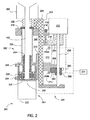
図2は、図1の堆積チャンバの一部分の断面詳細図である。図2は、プロセシングチャンバ内で基板を処理するために使用する基板支持部用の支持機構200を図示する。支持機構200は、支持シャフトアセンブリ202およびリフトアセンブリ250を備える。支持シャフトアセンブリ202を、支持ブラケット204によってリフトアセンブリ250に連結する。支持ブラケット204は、開口部(図示せず)を有し、支持シャフトアセンブリ202の構成要素をリフトアセンブリ250の構成要素に連結することを可能にする。
2 is a detailed cross-sectional view of a portion of the deposition chamber of FIG. FIG. 2 illustrates a
リフトアセンブリ250は、リフトアクチュエータ256に連結されたリフトモータ252を備える。リフトアクチュエータ256を、ある実施形態ではリフトモータ252に回転可能に連結されたネジ型アクチュエータとすることができる。リフトアクチュエータ256を、リフトカップリング258に連結する。リフトカップリング258は、下記にさらに詳細に説明するように、支持シャフトアセンブリ202の構成要素に連結する。リフトアクチュエータ256がネジ型アクチュエータである実施形態では、リフトカップリング258をねじ込みカラーとすることができる。ねじ込みリフトカラーおよびネジ型リフトアクチュエータを取り上げた実施形態では、リフトカラーは、リフトカラー上のネジ山とかみ合うリフトアクチュエータ上のネジ山によってリフトアクチュエータの縦方向に沿って支えられて動く。モータがリフトアクチュエータを回すので、リフトカラー上のネジ山とかみ合ったリフトアクチュエータ上のネジ山は、縦方向にリフトアクチュエータに沿ってリフトカラーを強制的に動かす。代替実施形態では、リフトカップリング258を、レールまたはロッドに沿って滑るネジ山のないカラーとかみ合うグライドカップリングとすることができ、レールまたはネジ山のないカラーの、どちらもリフトモータ252に連結されたリニアアクチュエータによってアクチュエートすることができる。
The
リフトアクチュエータ256が回転する実施形態では、固定具(図示せず)により圧縮シート262に連結された圧縮ブラケット260によって、リフトカップリング258が回転することを防止することができる。リフトカップリング258への圧縮ブラケット260および圧縮シート262の適用は、回転を防止するリフトカップリング258に摩擦力を結果としてもたらす。別の一実施形態では、リフトアクチュエータ256に実質的に平行なガイドロッドを設け、リフトカップリング258の一部分を通過させることによって、リフトカップリング258が回転することを防止することができる。かかる実施形態では、リフトアクチュエータ256を具備するリフトカップリング258の回転を防止するロッドガイドに沿って、リフトカップリング258は支えられて動くことができる。他の代替実施形態では、モータ252に固定された、レールなどの部材中の溝とかみ合うことが可能であるリフトカップリング258の外側表面上に突起部またはタブを設けることによるなどの他の方法で、ネジ山付きリフトカラーが回転することを防止することができる。
In an embodiment in which the
支持シャフトアセンブリ202は、支持シャフト140や、回転アセンブリ240や、チャンバカップリング220や、上部ベローズ232や、下部ベローズ234を備える。支持シャフト140は、表面116の回転運動および移動運動をもたらすために支持シャフト140の第1の終端部120(図1)のところで基板支持部117の表面116と連結し、支持シャフト140の第2の終端部230のところで回転アセンブリ240と連結する。回転アセンブリ240は、支持シャフト140および回転モータ222に連結された支持カップ214を備える。支持カップ214は、回転モータ222に連結され、ロータ226に磁気的に連結された磁気アクチュエータ224を備える。磁気ロータとすることができるロータ226は、支持シャフト140に取り付けられ、回転モータ222から支持シャフト140への回転動作を伝える。
The
回転アセンブリ240を第1のリフト部材206によってリフトアセンブリ250と連結する。第1のリフト部材206は、回転アセンブリ240をリフトカップリング258に連結する第1の伸展部208を備える。第1の伸展部208は、支持ブラケット204を通って延び、リフトカップリング258または圧縮シート262または両方に連結する。リフトカップリング258が動くにつれて、第1のリフト部材206は、それに従って支持シャフトアセンブリ202を動かす。第1のリフト部材206は、やはりある実施形態では、支持板210を備えることができる。支持板210は、支持ブラケット204中のチャネルまたは開口部とかみ合う突起部または伸展部(図示せず)によって支持シャフトアセンブリ202の動作を一次元にほぼ束縛する。
The
支持シャフトアセンブリ202は、第2のリフト部材216をさらに備える。第2のリフト部材216を、第2の伸展部218および弾性部材266によってリフトアセンブリ250に連結する。リフトピン170が第2のリフト部材216とともに進むように、第2の伸展部218は、やはり、リフトピンアクチュエータ228によって、図1のリフトピンカラー174およびリフトピン170などのリフトピンアセンブリに支持機構200を連結する。弾性部材266によって支持ブラケット204に取り付けることができる、モータマウント264などのリフトアセンブリ250の動かない部分に、第2の伸展部218を弾性的にかみ合わせる。一実施形態では、弾性部材266はスプリングであるが、変形したときに復元力を与える任意の部材を使用することができる。例えば、ある実施形態では、弾性部材266をポリマのパッドまたはクッションとすることができる。
The
第2のリフト部材216は、下部ベローズ234によって支持シャフトアセンブリ202とともに動く。第2のリフト部材216の移動は、しかしながら、リフトアセンブリ250の構成によって束縛される。第2のリフト部材216がプロセシングチャンバに向けて動くにつれて、復元力が弾性部材266中に生じ、第2のリフト部材216がプロセシングチャンバから離れることを促すようにする。それに加えて、支持ブラケット204またはモータマウント264などのリフトアセンブリ250に動かないように固定された任意の構成に対して所望の場所に、上部止め具268を設置する。第2のリフト部材216が上部止め具268に突き当たるときに、プロセシングチャンバに向けての第2のリフト部材216の移動が止まる。
リフトアセンブリ250の構成は、やはり、第2のリフト部材216の戻りを束縛する。第2のリフト部材216がプロセシングチャンバから遠くへと動くにつれて、復元力が弾性部材266中に生じ、プロセシングチャンバに向けて第2のリフト部材を促すようにする。それに加えて、第2のリフト部材216の戻りを束縛するために、下部止め具270をやはり設ける。図2の実施形態では、モータマウント264には、第2の伸展部218によって第2のリフト部材216用の下部止め具270を設けてある。第2の伸展部218が下部止め具270に突き当たるときに、プロセシングチャンバから離れる第2のカップリングブラケットの移動が止まる。図2の実施形態が下部止め具としてのモータマウント264の使用を取り上げているが、他の実施形態は、下部止め具として設けられるもう1つの部材を取り上げることができる。支持ブラケット204か、モータマウント264か、またはモータ252に固定することによってなどで、任意のかかる部材をリフトアセンブリ250に固定することができる。
The configuration of the
支持シャフト140がリフトモータ252によって下降するので、第2のリフト部材216は、下部ベローズ234によって支持シャフト140とともに初めは進み、従って、基板支持部117とともにリフトピン170(図1)を下降させる。第2の伸展部218が下部止め具270に近づくにつれて、復元力が弾性部材266中に生じる。第2の伸展部218が下部止め具270に突き当たるときに、第2のリフト部材216が動きを止め、やはり、リフトピン170(図1)が動きを止める。支持シャフト140が動き続けるので、基板支持部117(図1)は、下降し続けるが、リフトピン170(図1)は止まったままである。リフトピン(170)は、従って、基板支持部117の表面116の上方に突き出し、基板支持部117の上方に基板114を持ち上げる。
Since the
支持シャフト140をリフトモータ252によって上昇させたときに、弾性部材266の復元力、下部ベローズ234中の張力が、弾性部材266中の復元力に初めは打ち勝ち、下部止め具270に対して第2の伸展部218を保持し、定位置にリフトピン170(図1)を保つ。基板支持部117は、従って、リフトピン170によって基板支持部117の上方に保持された基板114に近づく。弾性部材266の復元力が下部ベローズ234中の張力に打ち勝つ点まで支持シャフト140を上昇させたときに、第2のリフト部材216は、支持シャフト140とともに動き始め、リフトピン170もやはり、基板支持部117とともに動き始める。弾性部材266が平衡位置に到達するので、基板114が基板支持部117上に配置されるように、リフトピン170が引っ込む。
When the
第2の伸展部218が上部止め具268に到達するときに、第2のリフト部材216およびリフトピン170(図1)は動きを止める。支持シャフト140および基板支持部117は、プロセシング位置へと基板114を動かし続ける。従って、リフトピン170と基板支持部117との間の距離が大きくなる。この距離は、リフトピン170を危険にさらすことなく基板支持部117が回転することを可能にする。
When the
支持シャフト140がプロセシングチャンバ中へと進み、プロセシングチャンバが低い圧力にほぼ維持されるため、プロセシングチャンバ内部の反応ゾーンの汚染を避けるために、支持シャフト140を低い圧力環境に概して維持する。上部ベローズ232は、第2のリフト部材216とチャンバカップリング220との間に低圧筐体を形成する。下部ベローズ234は、第2のリフト部材216と第1のリフト部材206との間に低圧筐体を形成する。このようにして、支持シャフト140をプロセシングチャンバと同じ圧力に維持された環境中に収納することができる。
センサ板272を、例えば、支持ブラケット204に固定することによってリフトアセンブリ250に連結することができる。センサ板272は、リフト機構の動作を制御するために使用することができるセンサをマウントするための場所を提供する。図2の実施形態は、2つのセンサ268Aおよび268Bを取り上げている。センサ268Aおよび268Bを、光−電子スイッチまたは圧力スイッチなどの、リフトアセンブリ250に対する支持シャフトアセンブリ202の接近または通過を検出することが可能な任意のタイプのセンサとすることができる。センサ268Bを、支持シャフトアセンブリ202がホーム位置に到達したときにリフトモータ252をオフに切り換えるホームセンサとすることができる。センサ268Aを回転モータ222に連結することができ、リフトシャフトアセンブリがセンサ268Aを通過したときにリフトシャフトの回転を可能にするインターロック能力を与える。基板支持部117とリフトピン170との間の最小クリアランスを作る支持シャフト140の位置を指示するように、センサ268Aを設置することができる。センサ268Aからの信号に応じて回転モータ222の電源を入れ、電源を切り、センサ268Bからの信号に応じてリフトモータ252の電源を入れ、電源を切るコントローラ274に、センサ268A/Bを、やはり連結することができる。
The
基板支持部117が中心軸102に平行な方向に動く間に、回転インターロックセンサとして機能するセンサ268Aが、基板114(図1)の回転を可能にすることに、留意すべきである。この能力は、プロセシング位置へと基板114を動かしつつ回転を実現することによってチャンバ内での全体のプロセシング時間を短縮する。それに加えて、図2のリフト機構200は、支持シャフト140によって基板支持部117の精密な制御を可能にし、その結果、基板支持部117を、最大速度で基板114に向けて上昇させ、基板支持部117と基板114との間の小さな力の接触をもたらすために、基板114に接触する直前に減速させることができる。小さな力の接触は、基板の物理的な破砕およびそれによる微粒子発生を最小にする。最後に、基板の回転および移動の独立した制御は、大きなプロセスウィンドウを可能にする。例えば、堆積反応を制御するために、基板を流路152Nに対して任意の点のところに設置することができる。一実施形態では、基板を、流路152Nの約0.6インチ(15.2mm)下方と流路152Nの約0.2インチ(5.1mm)上方との間に回転可能に設置することができる。他の実施形態では、基板の位置を、回転を止めずに反応中に変更することができる。従って、堆積の進行を制御し、堆積する膜の特性をうまく操作するために、位置プロファイルを反応中に実行することができる。
It should be noted that the
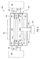
同時の軸運動および回転運動を具備する支持機構200は、やはり、プロセシングチャンバ内の異なるレベルのところで、すなわちプロセシングチャンバの異なるプロセシングゾーン中で基板を処理することを可能にする。図3は、堆積チャンバ300の別の一実施形態の概略的断面図である。チャンバ300は、内部体積342を画定する筐体302を備える。基板支持部304を、チャンバ300の内部体積342内に配置し、筐体302の開口部344を通り延びるシャフト308によってアクチュエータ306に連結する。アクチュエータ306は、回転させながら、チャンバ300の内部体積342内の異なるプロセシング位置312および314へと基板支持部を動かす。チャンバ300の内部体積342にエネルギーを加えるために、各々を一塊の加熱ランプとすることができるエネルギー源322および324を、別々にまたは一緒に使用することができる。
The
チャンバ300は、内部体積342内でプロセシングゾーンを画定する1個または複数の端部リング348をさらに備える。端部リング348は、5個までの端部リング、例えば、1個と5個との間の端部リングを備えることができる。ある実施形態では、チャンバは、複数の端部リングを有することができる。図3の実施形態では、3個の端部リング316、318および320を示す。
The
各端部リングは、少なくとも1つのプロセシングゾーンの境界、およびプロセシングゾーンの低い方を画定するために基板支持部304を設置する開口部を画定する。例えば、第1のプロセシングゾーンは、第1の端部リングおよび第1の端部リングの上方の第2の端部リングによって画定される。第1のプロセシングゾーンの下側境界は、第1の端部リングによって画定され、第1のプロセシングゾーンの上側境界は、第2の端部リングによって画定され、第2の端部リングはやはり、第1のプロセシングゾーンの上方の第2のプロセシングゾーンの下側境界を画定することができる。基板支持部を第1の端部リングに近接して設置するとき、第1の端部リングによって画定される開口部内では、基板支持部が第1のプロセシングゾーンのためのフロアを与え、基板がその中で処理される。
Each end ring defines an opening in which to place the
複数の端部リング348は、基板支持部304の肩部350の上方に突き出して延びる1個の端部リング320を備え、その端部リング320は通常はチャンバの最上部の端部リングである。他の端部リング、例えば、図3の端部リング316および318は、端部リングによって画定される様々なプロセシングゾーンにアクセスするために基板支持部304が通過することができる開口部を、各々が有する。
The plurality of end rings 348 include a
基板支持部が端部リング316および318に近接して設置されるので、第1のギャップおよび第2のギャップ、それぞれ352および354は、端部リング316および318の内径ならびに基板支持部304の端部部分356によって画定される。例えば、第1の端部リング316は、基板支持部を第1の端部リング316に近接して設置するときに、第1の端部リング316の内径と基板支持部304の端部部分356との間のギャップ352を画定し、第2の端部リング318は、基板支持部を第2の端部リング318に近接して設置するときに、第2の端部リング318の内径と基板支持部304の端部部分356との間のギャップ354を画定する。
Since the substrate support is located proximate to the end rings 316 and 318, the first gap and the second gap, 352 and 354, respectively, are the inner diameter of the end rings 316 and 318 and the end of the
ギャップ352および354、または3個よりも多くのまたは少ない端部リング取り上げる実施形態における、端部リングと基板支持部304との間のすべてのかかるギャップは、チャンバの幾何学的形状および所望のプロセシング特性に応じて幅が変わることがある。大部分の実施形態では、ギャップは、基板支持部304の端部部分356とチャンバ筐体302との間の距離「D」の約0.5%と約75%との間の幅「W」をそれぞれが有する。300mm基板を処理するように適合したチャンバでは、ギャップは、約1mmと約100mmとの間の幅をそれぞれが有することができる。ある実施形態では、ギャップは、すべてが同じ幅Wを有することができるが、図3に示したものなどの他の実施形態では、ギャップは、異なる幅Wを有することができる。例えば、図3に示したように、ギャップ354は、ギャップ352の幅Wより小さな幅Wを有することができる。
All such gaps between the end rings and the
ガスは、各々がプロセシングゾーンに連結された複数のガス導管を介し、端部リングによって画定される様々なプロセシングゾーンに供給される。図3では、3つのガス導管326、328および330は、それぞれ端部リング316、318および320によって画定される3つのプロセシングゾーンにガスを供給する。1つのガス源338が3つのガス導管326、328および330にガスを供給するように示されているが、複数のガス源をやはり、いかなる考え得る構成においても任意の数の導管を与えるために使用することができる。ガスはチャンバから、順に、ガス導管と同様にそれぞれがプロセシングゾーンに連結されている複数の排出導管を介して排出される。図3では、3つの排出導管332、334および336が排出システム340にガスを排出し、その排出システム340は、いかなる考え得る構成においても、任意の数の導管に連結された任意の数の排出システムを表わすことができる。
Gas is supplied to the various processing zones defined by the end rings via a plurality of gas conduits each connected to the processing zone. In FIG. 3, three
基板は最下部のプロセシングゾーンの下方の開口部310を通ってチャンバに供給され、チャンバから取り出される。図2に関連して上に論じたように、基板支持部304が開口部310に近接するローディング位置またはアンローディング位置に接近すると、リフト機構は、近接センサまたはスイッチの動作よって回転機構を止め、リフトピンは配置につく。
The substrate is fed into the chamber through the
動作では、基板支持部は、端部リング318などの端部リングのうちの1つに近接して設置される。図3の実施形態ではガス導管328であり、端部リング318および基板支持部304によって画定されるプロセシングゾーンを取り扱う導管を介してガスを供給する。堆積プロセスを実行するために、ガスは基板支持部304上に配置された基板を横切って流れ、余分なガスは、排出導管334を介して排出システム340へと流れ出る。反応ガスが隣接するゾーンを介してアクティブなプロセシングゾーンから逃げることを防止するために、アクティブなプロセシングゾーンの上方および/または下方のプロセシングゾーンを介して、ガスをやはり供給することができる。例えば、端部リング318によって画定される下側境界のあるゾーン内での処理中に、端部リング320の上方および端部リング318の下方のゾーン中の反応性ガス濃度を最小にするために、ガス導管330および326を介して非反応性ガスまたはパージガスを供給することができる。
In operation, the substrate support is placed proximate to one of the end rings, such as
第1のプロセシングゾーン内での処理後に、基板支持部304の軸に沿って動かすことによって、基板支持部304を第2のプロセシングゾーンへと動かす。非生産時間を最小にするために、プロセシングゾーン間の移動中に、基板支持部の回転を維持する。処理に直ちに取り掛かるように、基板支持部を位置へと移動させる前に、第2のプロセシングゾーン中でのプロセシング条件を設定することができる。
After processing in the first processing zone, the
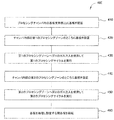
図4は、別の一実施形態による方法400を要約した流れ図である。方法400は、ALDプロセスや、CVDプロセスや、エピタキシプロセスや、エッチプロセスなどの半導体基板上に周期的なプロセスを実行するために有用である。
FIG. 4 is a flow diagram summarizing a
410において、プロセシングチャンバ内の基板支持部上に基板を配置する。図3のチャンバ300などのプロセシングチャンバを、方法400を実施するために使用することができる。
At 410, a substrate is placed on a substrate support in the processing chamber. A processing chamber such as
420において、プロセスチャンバ内側の第1のプロセシングゾーンのところに基板を設置する。410におけるローディング位置またはアンローディング位置から第1のプロセシングゾーンへと基板支持部を動かす。ある実施形態では、第1のプロセシングゾーンを、第1の仕切りによって画定することができ、第1の仕切りを、第1のプロセシングゾーンを画定する第1の複数の仕切りとすることができる。基板支持部が第1の仕切りに近接する位置に動くので、基板支持部上に配置された基板は、第1のプロセシングゾーンに入る。
At 420, a substrate is placed at a first processing zone inside the process chamber. The substrate support is moved from the loading or unloading position at 410 to the first processing zone. In certain embodiments, the first processing zone can be defined by a first partition, and the first partition can be a first plurality of partitions that define a first processing zone. Since the substrate support portion moves to a position close to the first partition, the substrate disposed on the substrate support portion enters the first processing zone.
430において、第1のプロセシングゾーン内の基板上に、第1のプロセシングサイクルを実行する。第1のガスを第1のプロセシングゾーンに供給し、基板支持部またはプロセシングチャンバの内側または外側に設置した別の1つのエネルギー源を使用して、エネルギーを加えることができる。一実施形態では、処理中に基板を加熱するために、熱源をチャンバの上方もしくは下方または両方に設置することができる。一実施形態では、基板温度および基板上方の圧力などのプロセシング条件を、基板が第1のプロセシングゾーンに到達する時点で実現することができる。他の実施形態では、基板支持部を設置する前に、所望のプロセシング条件を第1のプロセシングゾーン内に設定することができる。どちらの実施形態でも、基板が第1のプロセシングゾーンに入ったときに、処理を直ちに始めることができる。 At 430, a first processing cycle is performed on a substrate in the first processing zone. A first gas can be supplied to the first processing zone and energy can be applied using another energy source located inside or outside the substrate support or processing chamber. In one embodiment, a heat source can be placed above or below the chamber or both to heat the substrate during processing. In one embodiment, processing conditions such as substrate temperature and pressure above the substrate can be realized when the substrate reaches the first processing zone. In other embodiments, the desired processing conditions can be set in the first processing zone prior to installing the substrate support. In either embodiment, processing can begin immediately when the substrate enters the first processing zone.
440において、基板支持部を動かすことによって、基板を第2のプロセシングゾーンのところに設置する。第1のプロセシングゾーンと同様に、1つのプロセシングゾーンから別の1つへのガスのクロスフローを最小にするために、第2のプロセシングゾーンを第2の仕切りによって画定することができる。ガスカーテンをやはり、プロセシングゾーン間に設けることができる。ガスカーテンは、やはり、2つの堆積操作またはエッチ操作間に冷却操作を実行するために有用であり得る。ガスカーテンは、やはり、操作間に基板表面から反応物をパージするために有用であり得る。 At 440, the substrate is placed at the second processing zone by moving the substrate support. Similar to the first processing zone, the second processing zone can be defined by a second partition to minimize the cross-flow of gas from one processing zone to another. A gas curtain can again be provided between the processing zones. The gas curtain can again be useful for performing a cooling operation between two deposition or etch operations. The gas curtain can also be useful for purging reactants from the substrate surface during operation.
450において、第2のプロセシングゾーン内の基板上に、第2のプロセシングサイクルを実行する。第2のガスを第2のプロセシングゾーンに供給する。第1のプロセシングゾーンで用いたように、同じエネルギー源または異なるエネルギー源を使用して、エネルギーを第2のプロセシングゾーンに加えることができる。例えば、第1のプロセシングゾーンが第1のエネルギー源に近接し、第2のプロセシングゾーンが第2のエネルギー源に近接する場合には、第1のプロセシングサイクル中に第1のエネルギー源を使用することができ、第2のプロセシングサイクル中に第2のエネルギー源を使用することができる。 At 450, a second processing cycle is performed on the substrate in the second processing zone. A second gas is supplied to the second processing zone. As used in the first processing zone, energy can be applied to the second processing zone using the same energy source or different energy sources. For example, if the first processing zone is proximate to the first energy source and the second processing zone is proximate to the second energy source, the first energy source is used during the first processing cycle. And a second energy source can be used during the second processing cycle.
460において、基板を処理中に間回転させ、基板を処理し設置している間、回転を維持する。回転が有利でないプロセスサイクルに対して、回転を止めることができ、その後、回転が望まれる引き続くプロセスサイクルに対して再開することができる。基板が次のプロセシングゾーンに入るときに処理を直ちに開始することができるように、概して、プロセシングゾーン間で基板を動かしつつ、回転を維持する。所望のRPMを実現するために、回転を待つために時間を浪費しない。 At 460, the substrate is rotated during processing and the rotation is maintained while the substrate is processed and installed. For process cycles where rotation is not advantageous, rotation can be stopped and then resumed for subsequent process cycles where rotation is desired. In general, rotation is maintained while moving the substrate between the processing zones so that processing can begin immediately when the substrate enters the next processing zone. No time is wasted waiting for rotation to achieve the desired RPM.
例示的な一実施形態では、図3のチャンバ300に類似の3つのプロセシングゾーンを有するチャンバを、ALDプロセスを効率的に実行するために使用することができる。基板上に第1の前駆体を堆積させるためのプロセシング条件を、第1のプロセシングゾーン、例えば、最下部のプロセシングゾーンに設定することができ、第1の前駆体と反応するために第2の前駆体を堆積させるための条件を、第2のプロセシングゾーンに設定することができる。ALD堆積を実行することは、次に、指示されたやり方で2つのプロセシングゾーン間で基板を動かすことになる。基板がゾーン間を動くので、基板からのどんな余分な反応物でも除去するために、ガスカーテンをプロセシングゾーン間に設けることができる。ALDプロセスを第1のプロセシングゾーンおよび第2のプロセシングゾーン内で実行した後で、望まれる場合には、クリーニング操作を、第3のプロセシングゾーン内で実行することができる。
In one exemplary embodiment, a chamber having three processing zones similar to
別の例示的な一実施形態では、隣接するプロセシングゾーンに2つのプロセスのためのプロセス条件を設定し、指示されたやり方でこれらのゾーン間で基板を動かすことによって、逐次的な堆積プロセスおよびエッチプロセスをかかるチャンバ内で実行することができる。使用されていないプロセシングゾーン内でプロセシング条件を調節することによって、3つ以上の多くの操作を伴う長く複雑なプロセスを実行するために、3つ以上のプロセシングゾーンを有するプロセシングチャンバを使用することができることに、留意すべきである。例えば、3つの異なるプロセシングゾーンにおいて3つの操作を実行した後で、基板上に4番目の操作や、5番目の操作や、または追加の操作を実行するために、使用されていないプロセシングゾーンのプロセシング条件を変更することができる。 In another exemplary embodiment, a sequential deposition process and etch is performed by setting process conditions for two processes in adjacent processing zones and moving the substrate between these zones in the manner indicated. The process can be performed in such a chamber. Using a processing chamber with more than two processing zones to perform a long and complex process with more than two operations by adjusting the processing conditions within the unused processing zones It should be noted that it can be done. For example, after performing three operations in three different processing zones, processing a processing zone that is not being used to perform a fourth, fifth, or additional operation on the substrate. Conditions can be changed.
ある実施形態では、プロセシングゾーンに設定したプロセシング条件は、活性化した前駆体を必然的に含むことがある。一実施形態では、遠くで活性化した前駆体を1つまたは複数のプロセシングゾーンに供給することができる。活性化していない前駆体または不活性な前駆体でさえも、隣接するプロセシングゾーンに供給しつつ、遠くで活性化した前駆体を1つのプロセシングゾーンに供給することができる。一実施形態では、最上部のプロセシングゾーンまたは最下部のプロセシングゾーン内に誘導結合プラズマを生成させるための誘導源に隣接して、プロセシングゾーン、例えば、最上部のプロセシングゾーンまたは最下部のプロセシングゾーンを設置することができる。プロセシングゾーン内の反応を促進させるように選択した電力レベルで所望のプロセシングゾーンへとエネルギーを結合させ、一方で隣接するプロセシングゾーン内では反応を促進させるために必要なものよりも低いレベルに低下させる方法で、誘導源を動作させることができる。かかる条件は、操作のより大きなシーケンスの一部としてプラズマ堆積操作か、プラズマエッチ操作か、またはプラズマクリーニング操作を実行するために有用であり得る。必要であれば、あるプロセシングゾーンにおけるある操作に対して望まれる場合には、電気的なバイアスを基板支持部に結合させることができる。 In certain embodiments, the processing conditions set in the processing zone may necessarily include activated precursors. In one embodiment, remotely activated precursors can be provided to one or more processing zones. Distant activated precursors can be fed into one processing zone while feeding unactivated precursors or even inactive precursors into adjacent processing zones. In one embodiment, a processing zone, e.g., a top processing zone or a bottom processing zone, is adjacent to an inductive source for generating an inductively coupled plasma in the top processing zone or the bottom processing zone. Can be installed. Bind energy to the desired processing zone at a power level selected to promote the reaction in the processing zone, while reducing it to a lower level in the adjacent processing zone than is necessary to promote the reaction In the manner, the induction source can be operated. Such conditions can be useful for performing a plasma deposition operation, a plasma etch operation, or a plasma cleaning operation as part of a larger sequence of operations. If desired, an electrical bias can be coupled to the substrate support if desired for certain operations in certain processing zones.
前述は本発明の実施形態に向けられているが、本発明の他の実施形態およびさらなる実施形態を、本発明の基本的な範囲から乖離せずに考案することができる。 While the foregoing is directed to embodiments of the invention, other and further embodiments of the invention may be devised without departing from the basic scope thereof.
Claims (15)
前記プロセスチャンバの内部体積を画定する筐体と、
前記筐体に沿って配置された1個または複数の端部リングであって、各端部リングが前記プロセスチャンバの前記内部体積内で少なくとも1つのプロセシングゾーンの境界を画定する、端部リングと、
前記チャンバの前記内部体積内に配置され、基板支持部の中心軸に平行な方向に動かしながら前記中心軸の周りを回転させるように構成された、基板支持部と、
前記プロセシングチャンバの各プロセシングゾーンに連結されたガス導管と
を備える、プロセスチャンバ。 A process chamber for processing a semiconductor substrate, comprising:
A housing defining an internal volume of the process chamber;
One or more end rings disposed along the housing, each end ring defining at least one processing zone boundary within the interior volume of the process chamber; ,
A substrate support disposed within the internal volume of the chamber and configured to rotate about the central axis while moving in a direction parallel to the central axis of the substrate support;
And a gas conduit coupled to each processing zone of the processing chamber.
プロセシングチャンバ内の基板支持部上に前記基板を設置するステップと、
前記基板支持部上の前記基板を回転させるステップと、
前記基板を回転させながら回転の軸に沿って前記基板を動かすステップと
を備える方法。 A method for processing a semiconductor substrate, comprising:
Placing the substrate on a substrate support in a processing chamber;
Rotating the substrate on the substrate support;
Moving the substrate along an axis of rotation while rotating the substrate.
前記基板の回転を維持するステップと、
第2のプロセシングゾーンへ前記回転の軸に沿って前記基板を動かすステップと、
前記第2のプロセシングゾーン内で前記基板を処理するステップと
をさらに備える、請求項7に記載の方法。 Processing the substrate in a first processing zone;
Maintaining the rotation of the substrate;
Moving the substrate along the axis of rotation to a second processing zone;
The method of claim 7, further comprising processing the substrate in the second processing zone.
を備えるプロセスチャンバであって、前記基板支持部が、
前記プロセスチャンバのフロアを通って延びる支持シャフトの第1の終端部に連結され、前記支持シャフトの第2の終端部のところで回転アセンブリに連結された基板支持部表面と、
前記回転アセンブリおよびリフトアクチュエータに連結された第1のリフト部材ならびに、前記支持シャフトおよびリフトピンアクチュエータに連結された第2のリフト部材を備えるリフトアセンブリと
を備える、プロセスチャンバ。 A process chamber comprising a substrate support disposed within the process chamber, wherein the substrate support is
A substrate support surface coupled to a first end of a support shaft extending through the floor of the process chamber and coupled to a rotating assembly at a second end of the support shaft;
A process chamber comprising: a first lift member coupled to the rotary assembly and a lift actuator; and a lift assembly comprising a second lift member coupled to the support shaft and a lift pin actuator.
Applications Claiming Priority (5)
| Application Number | Priority Date | Filing Date | Title |
|---|---|---|---|
| US9869908P | 2008-09-19 | 2008-09-19 | |
| US61/098,699 | 2008-09-19 | ||
| US12/560,073 | 2009-09-15 | ||
| US12/560,073 US20100075488A1 (en) | 2008-09-19 | 2009-09-15 | Cvd reactor with multiple processing levels and dual-axis motorized lift mechanism |
| PCT/US2009/057252 WO2010033659A1 (en) | 2008-09-19 | 2009-09-17 | Cvd reactor with multiple processing levels and dual-axis motorized lift mechanism |
Publications (2)
| Publication Number | Publication Date |
|---|---|
| JP2012503338A true JP2012503338A (en) | 2012-02-02 |
| JP2012503338A5 JP2012503338A5 (en) | 2012-08-23 |
Family
ID=42038097
Family Applications (1)
| Application Number | Title | Priority Date | Filing Date |
|---|---|---|---|
| JP2011527949A Pending JP2012503338A (en) | 2008-09-19 | 2009-09-17 | CVD reactor having a plurality of processing levels and a biaxial motor lift mechanism |
Country Status (6)
| Country | Link |
|---|---|
| US (1) | US20100075488A1 (en) |
| JP (1) | JP2012503338A (en) |
| KR (1) | KR20110056553A (en) |
| CN (1) | CN102160147A (en) |
| TW (1) | TW201017726A (en) |
| WO (1) | WO2010033659A1 (en) |
Cited By (1)
| Publication number | Priority date | Publication date | Assignee | Title |
|---|---|---|---|---|
| JP2015043420A (en) * | 2013-08-13 | 2015-03-05 | ラム リサーチ コーポレーションLam Research Corporation | Plasma processing devices having multi-port valve assemblies |
Families Citing this family (198)
| Publication number | Priority date | Publication date | Assignee | Title |
|---|---|---|---|---|
| JP4523661B1 (en) * | 2009-03-10 | 2010-08-11 | 三井造船株式会社 | Atomic layer deposition apparatus and thin film forming method |
| US20120270384A1 (en) * | 2011-04-22 | 2012-10-25 | Applied Materials, Inc. | Apparatus for deposition of materials on a substrate |
| US9512520B2 (en) * | 2011-04-25 | 2016-12-06 | Applied Materials, Inc. | Semiconductor substrate processing system |
| US20130023129A1 (en) | 2011-07-20 | 2013-01-24 | Asm America, Inc. | Pressure transmitter for a semiconductor processing environment |
| US9499905B2 (en) * | 2011-07-22 | 2016-11-22 | Applied Materials, Inc. | Methods and apparatus for the deposition of materials on a substrate |
| US20130052333A1 (en) * | 2011-08-22 | 2013-02-28 | Soitec | Deposition systems having reaction chambers configured for in-situ metrology and related methods |
| US9644285B2 (en) | 2011-08-22 | 2017-05-09 | Soitec | Direct liquid injection for halide vapor phase epitaxy systems and methods |
| JP5807511B2 (en) * | 2011-10-27 | 2015-11-10 | 東京エレクトロン株式会社 | Film forming apparatus and operation method thereof |
| US9682398B2 (en) | 2012-03-30 | 2017-06-20 | Applied Materials, Inc. | Substrate processing system having susceptorless substrate support with enhanced substrate heating control |
| US10714315B2 (en) | 2012-10-12 | 2020-07-14 | Asm Ip Holdings B.V. | Semiconductor reaction chamber showerhead |
| US20160376700A1 (en) | 2013-02-01 | 2016-12-29 | Asm Ip Holding B.V. | System for treatment of deposition reactor |
| US10941490B2 (en) | 2014-10-07 | 2021-03-09 | Asm Ip Holding B.V. | Multiple temperature range susceptor, assembly, reactor and system including the susceptor, and methods of using the same |
| SG11201705062PA (en) * | 2015-02-17 | 2017-09-28 | Applied Materials Inc | Apparatus for adjustable light source |
| US10276355B2 (en) * | 2015-03-12 | 2019-04-30 | Asm Ip Holding B.V. | Multi-zone reactor, system including the reactor, and method of using the same |
| US10458018B2 (en) | 2015-06-26 | 2019-10-29 | Asm Ip Holding B.V. | Structures including metal carbide material, devices including the structures, and methods of forming same |
| US10211308B2 (en) | 2015-10-21 | 2019-02-19 | Asm Ip Holding B.V. | NbMC layers |
| US11139308B2 (en) | 2015-12-29 | 2021-10-05 | Asm Ip Holding B.V. | Atomic layer deposition of III-V compounds to form V-NAND devices |
| US10529554B2 (en) | 2016-02-19 | 2020-01-07 | Asm Ip Holding B.V. | Method for forming silicon nitride film selectively on sidewalls or flat surfaces of trenches |
| US11453943B2 (en) | 2016-05-25 | 2022-09-27 | Asm Ip Holding B.V. | Method for forming carbon-containing silicon/metal oxide or nitride film by ALD using silicon precursor and hydrocarbon precursor |
| US10612137B2 (en) | 2016-07-08 | 2020-04-07 | Asm Ip Holdings B.V. | Organic reactants for atomic layer deposition |
| US9859151B1 (en) | 2016-07-08 | 2018-01-02 | Asm Ip Holding B.V. | Selective film deposition method to form air gaps |
| US9812320B1 (en) | 2016-07-28 | 2017-11-07 | Asm Ip Holding B.V. | Method and apparatus for filling a gap |
| US9887082B1 (en) | 2016-07-28 | 2018-02-06 | Asm Ip Holding B.V. | Method and apparatus for filling a gap |
| US11532757B2 (en) | 2016-10-27 | 2022-12-20 | Asm Ip Holding B.V. | Deposition of charge trapping layers |
| US10714350B2 (en) | 2016-11-01 | 2020-07-14 | ASM IP Holdings, B.V. | Methods for forming a transition metal niobium nitride film on a substrate by atomic layer deposition and related semiconductor device structures |
| KR102546317B1 (en) | 2016-11-15 | 2023-06-21 | 에이에스엠 아이피 홀딩 비.브이. | Gas supply unit and substrate processing apparatus including the same |
| KR20180068582A (en) | 2016-12-14 | 2018-06-22 | 에이에스엠 아이피 홀딩 비.브이. | Substrate processing apparatus |
| US11447861B2 (en) | 2016-12-15 | 2022-09-20 | Asm Ip Holding B.V. | Sequential infiltration synthesis apparatus and a method of forming a patterned structure |
| US11581186B2 (en) | 2016-12-15 | 2023-02-14 | Asm Ip Holding B.V. | Sequential infiltration synthesis apparatus |
| US10269558B2 (en) | 2016-12-22 | 2019-04-23 | Asm Ip Holding B.V. | Method of forming a structure on a substrate |
| JP6899217B2 (en) * | 2016-12-28 | 2021-07-07 | 株式会社Screenホールディングス | Board processing equipment, board processing method and board processing system |
| US11390950B2 (en) | 2017-01-10 | 2022-07-19 | Asm Ip Holding B.V. | Reactor system and method to reduce residue buildup during a film deposition process |
| US10468261B2 (en) | 2017-02-15 | 2019-11-05 | Asm Ip Holding B.V. | Methods for forming a metallic film on a substrate by cyclical deposition and related semiconductor device structures |
| US10770286B2 (en) | 2017-05-08 | 2020-09-08 | Asm Ip Holdings B.V. | Methods for selectively forming a silicon nitride film on a substrate and related semiconductor device structures |
| US10770314B2 (en) * | 2017-05-31 | 2020-09-08 | Taiwan Semiconductor Manufacturing Company, Ltd. | Semiconductor device, tool, and method of manufacturing |
| US11306395B2 (en) | 2017-06-28 | 2022-04-19 | Asm Ip Holding B.V. | Methods for depositing a transition metal nitride film on a substrate by atomic layer deposition and related deposition apparatus |
| KR20190009245A (en) | 2017-07-18 | 2019-01-28 | 에이에스엠 아이피 홀딩 비.브이. | Methods for forming a semiconductor device structure and related semiconductor device structures |
| US11374112B2 (en) | 2017-07-19 | 2022-06-28 | Asm Ip Holding B.V. | Method for depositing a group IV semiconductor and related semiconductor device structures |
| US10590535B2 (en) | 2017-07-26 | 2020-03-17 | Asm Ip Holdings B.V. | Chemical treatment, deposition and/or infiltration apparatus and method for using the same |
| US10692741B2 (en) | 2017-08-08 | 2020-06-23 | Asm Ip Holdings B.V. | Radiation shield |
| US10770336B2 (en) | 2017-08-08 | 2020-09-08 | Asm Ip Holding B.V. | Substrate lift mechanism and reactor including same |
| US11769682B2 (en) | 2017-08-09 | 2023-09-26 | Asm Ip Holding B.V. | Storage apparatus for storing cassettes for substrates and processing apparatus equipped therewith |
| US11830730B2 (en) | 2017-08-29 | 2023-11-28 | Asm Ip Holding B.V. | Layer forming method and apparatus |
| US11295980B2 (en) | 2017-08-30 | 2022-04-05 | Asm Ip Holding B.V. | Methods for depositing a molybdenum metal film over a dielectric surface of a substrate by a cyclical deposition process and related semiconductor device structures |
| US10658205B2 (en) | 2017-09-28 | 2020-05-19 | Asm Ip Holdings B.V. | Chemical dispensing apparatus and methods for dispensing a chemical to a reaction chamber |
| CN111344522B (en) | 2017-11-27 | 2022-04-12 | 阿斯莫Ip控股公司 | Including clean mini-environment device |
| KR102597978B1 (en) | 2017-11-27 | 2023-11-06 | 에이에스엠 아이피 홀딩 비.브이. | Storage device for storing wafer cassettes for use with batch furnaces |
| US10872771B2 (en) | 2018-01-16 | 2020-12-22 | Asm Ip Holding B. V. | Method for depositing a material film on a substrate within a reaction chamber by a cyclical deposition process and related device structures |
| CN111630203A (en) | 2018-01-19 | 2020-09-04 | Asm Ip私人控股有限公司 | Method for depositing gap filling layer by plasma auxiliary deposition |
| TW202325889A (en) | 2018-01-19 | 2023-07-01 | 荷蘭商Asm 智慧財產控股公司 | Deposition method |
| US11081345B2 (en) | 2018-02-06 | 2021-08-03 | Asm Ip Holding B.V. | Method of post-deposition treatment for silicon oxide film |
| US10755955B2 (en) * | 2018-02-12 | 2020-08-25 | Applied Materials, Inc. | Substrate transfer mechanism to reduce back-side substrate contact |
| US10896820B2 (en) | 2018-02-14 | 2021-01-19 | Asm Ip Holding B.V. | Method for depositing a ruthenium-containing film on a substrate by a cyclical deposition process |
| EP3737779A1 (en) | 2018-02-14 | 2020-11-18 | ASM IP Holding B.V. | A method for depositing a ruthenium-containing film on a substrate by a cyclical deposition process |
| KR102636427B1 (en) | 2018-02-20 | 2024-02-13 | 에이에스엠 아이피 홀딩 비.브이. | Substrate processing method and apparatus |
| US10975470B2 (en) | 2018-02-23 | 2021-04-13 | Asm Ip Holding B.V. | Apparatus for detecting or monitoring for a chemical precursor in a high temperature environment |
| US11473195B2 (en) | 2018-03-01 | 2022-10-18 | Asm Ip Holding B.V. | Semiconductor processing apparatus and a method for processing a substrate |
| US11629406B2 (en) | 2018-03-09 | 2023-04-18 | Asm Ip Holding B.V. | Semiconductor processing apparatus comprising one or more pyrometers for measuring a temperature of a substrate during transfer of the substrate |
| KR102646467B1 (en) | 2018-03-27 | 2024-03-11 | 에이에스엠 아이피 홀딩 비.브이. | Method of forming an electrode on a substrate and a semiconductor device structure including an electrode |
| US11230766B2 (en) | 2018-03-29 | 2022-01-25 | Asm Ip Holding B.V. | Substrate processing apparatus and method |
| TW202344708A (en) | 2018-05-08 | 2023-11-16 | 荷蘭商Asm Ip私人控股有限公司 | Methods for depositing an oxide film on a substrate by a cyclical deposition process and related device structures |
| KR102596988B1 (en) | 2018-05-28 | 2023-10-31 | 에이에스엠 아이피 홀딩 비.브이. | Method of processing a substrate and a device manufactured by the same |
| US11270899B2 (en) | 2018-06-04 | 2022-03-08 | Asm Ip Holding B.V. | Wafer handling chamber with moisture reduction |
| US11718913B2 (en) | 2018-06-04 | 2023-08-08 | Asm Ip Holding B.V. | Gas distribution system and reactor system including same |
| US11286562B2 (en) | 2018-06-08 | 2022-03-29 | Asm Ip Holding B.V. | Gas-phase chemical reactor and method of using same |
| US10797133B2 (en) | 2018-06-21 | 2020-10-06 | Asm Ip Holding B.V. | Method for depositing a phosphorus doped silicon arsenide film and related semiconductor device structures |
| KR102568797B1 (en) | 2018-06-21 | 2023-08-21 | 에이에스엠 아이피 홀딩 비.브이. | Substrate processing system |
| US11492703B2 (en) | 2018-06-27 | 2022-11-08 | Asm Ip Holding B.V. | Cyclic deposition methods for forming metal-containing material and films and structures including the metal-containing material |
| WO2020003000A1 (en) | 2018-06-27 | 2020-01-02 | Asm Ip Holding B.V. | Cyclic deposition methods for forming metal-containing material and films and structures including the metal-containing material |
| US10612136B2 (en) | 2018-06-29 | 2020-04-07 | ASM IP Holding, B.V. | Temperature-controlled flange and reactor system including same |
| US10388513B1 (en) | 2018-07-03 | 2019-08-20 | Asm Ip Holding B.V. | Method for depositing silicon-free carbon-containing film as gap-fill layer by pulse plasma-assisted deposition |
| US10755922B2 (en) | 2018-07-03 | 2020-08-25 | Asm Ip Holding B.V. | Method for depositing silicon-free carbon-containing film as gap-fill layer by pulse plasma-assisted deposition |
| US11456203B2 (en) * | 2018-07-13 | 2022-09-27 | Taiwan Semiconductor Manufacturing Co., Ltd | Wafer release mechanism |
| US11430674B2 (en) | 2018-08-22 | 2022-08-30 | Asm Ip Holding B.V. | Sensor array, apparatus for dispensing a vapor phase reactant to a reaction chamber and related methods |
| KR20200030162A (en) | 2018-09-11 | 2020-03-20 | 에이에스엠 아이피 홀딩 비.브이. | Method for deposition of a thin film |
| US11024523B2 (en) | 2018-09-11 | 2021-06-01 | Asm Ip Holding B.V. | Substrate processing apparatus and method |
| CN110970344A (en) | 2018-10-01 | 2020-04-07 | Asm Ip控股有限公司 | Substrate holding apparatus, system including the same, and method of using the same |
| US11232963B2 (en) | 2018-10-03 | 2022-01-25 | Asm Ip Holding B.V. | Substrate processing apparatus and method |
| KR102592699B1 (en) | 2018-10-08 | 2023-10-23 | 에이에스엠 아이피 홀딩 비.브이. | Substrate support unit and apparatuses for depositing thin film and processing the substrate including the same |
| KR102546322B1 (en) | 2018-10-19 | 2023-06-21 | 에이에스엠 아이피 홀딩 비.브이. | Substrate processing apparatus and substrate processing method |
| KR102605121B1 (en) | 2018-10-19 | 2023-11-23 | 에이에스엠 아이피 홀딩 비.브이. | Substrate processing apparatus and substrate processing method |
| US11087997B2 (en) | 2018-10-31 | 2021-08-10 | Asm Ip Holding B.V. | Substrate processing apparatus for processing substrates |
| KR20200051105A (en) | 2018-11-02 | 2020-05-13 | 에이에스엠 아이피 홀딩 비.브이. | Substrate support unit and substrate processing apparatus including the same |
| US11572620B2 (en) | 2018-11-06 | 2023-02-07 | Asm Ip Holding B.V. | Methods for selectively depositing an amorphous silicon film on a substrate |
| US10818758B2 (en) | 2018-11-16 | 2020-10-27 | Asm Ip Holding B.V. | Methods for forming a metal silicate film on a substrate in a reaction chamber and related semiconductor device structures |
| US11217444B2 (en) | 2018-11-30 | 2022-01-04 | Asm Ip Holding B.V. | Method for forming an ultraviolet radiation responsive metal oxide-containing film |
| KR102636428B1 (en) | 2018-12-04 | 2024-02-13 | 에이에스엠 아이피 홀딩 비.브이. | A method for cleaning a substrate processing apparatus |
| US11158513B2 (en) | 2018-12-13 | 2021-10-26 | Asm Ip Holding B.V. | Methods for forming a rhenium-containing film on a substrate by a cyclical deposition process and related semiconductor device structures |
| JP2020096183A (en) | 2018-12-14 | 2020-06-18 | エーエスエム・アイピー・ホールディング・ベー・フェー | Method of forming device structure using selective deposition of gallium nitride, and system for the same |
| TWI819180B (en) | 2019-01-17 | 2023-10-21 | 荷蘭商Asm 智慧財產控股公司 | Methods of forming a transition metal containing film on a substrate by a cyclical deposition process |
| KR20200091543A (en) | 2019-01-22 | 2020-07-31 | 에이에스엠 아이피 홀딩 비.브이. | Semiconductor processing device |
| TW202044325A (en) | 2019-02-20 | 2020-12-01 | 荷蘭商Asm Ip私人控股有限公司 | Method of filling a recess formed within a surface of a substrate, semiconductor structure formed according to the method, and semiconductor processing apparatus |
| KR20200102357A (en) | 2019-02-20 | 2020-08-31 | 에이에스엠 아이피 홀딩 비.브이. | Apparatus and methods for plug fill deposition in 3-d nand applications |
| TW202104632A (en) | 2019-02-20 | 2021-02-01 | 荷蘭商Asm Ip私人控股有限公司 | Cyclical deposition method and apparatus for filling a recess formed within a substrate surface |
| KR102626263B1 (en) | 2019-02-20 | 2024-01-16 | 에이에스엠 아이피 홀딩 비.브이. | Cyclical deposition method including treatment step and apparatus for same |
| TW202100794A (en) | 2019-02-22 | 2021-01-01 | 荷蘭商Asm Ip私人控股有限公司 | Substrate processing apparatus and method for processing substrate |
| KR20200108248A (en) | 2019-03-08 | 2020-09-17 | 에이에스엠 아이피 홀딩 비.브이. | STRUCTURE INCLUDING SiOCN LAYER AND METHOD OF FORMING SAME |
| KR20200108242A (en) | 2019-03-08 | 2020-09-17 | 에이에스엠 아이피 홀딩 비.브이. | Method for Selective Deposition of Silicon Nitride Layer and Structure Including Selectively-Deposited Silicon Nitride Layer |
| JP2020167398A (en) | 2019-03-28 | 2020-10-08 | エーエスエム・アイピー・ホールディング・ベー・フェー | Door opener and substrate processing apparatus provided therewith |
| KR20200116855A (en) | 2019-04-01 | 2020-10-13 | 에이에스엠 아이피 홀딩 비.브이. | Method of manufacturing semiconductor device |
| KR20200123380A (en) | 2019-04-19 | 2020-10-29 | 에이에스엠 아이피 홀딩 비.브이. | Layer forming method and apparatus |
| KR20200125453A (en) | 2019-04-24 | 2020-11-04 | 에이에스엠 아이피 홀딩 비.브이. | Gas-phase reactor system and method of using same |
| US11251067B2 (en) * | 2019-04-26 | 2022-02-15 | Applied Materials, Inc. | Pedestal lift for semiconductor processing chambers |
| KR20200130118A (en) | 2019-05-07 | 2020-11-18 | 에이에스엠 아이피 홀딩 비.브이. | Method for Reforming Amorphous Carbon Polymer Film |
| KR20200130121A (en) | 2019-05-07 | 2020-11-18 | 에이에스엠 아이피 홀딩 비.브이. | Chemical source vessel with dip tube |
| KR20200130652A (en) | 2019-05-10 | 2020-11-19 | 에이에스엠 아이피 홀딩 비.브이. | Method of depositing material onto a surface and structure formed according to the method |
| JP2020188255A (en) | 2019-05-16 | 2020-11-19 | エーエスエム アイピー ホールディング ビー.ブイ. | Wafer boat handling device, vertical batch furnace, and method |
| USD947913S1 (en) | 2019-05-17 | 2022-04-05 | Asm Ip Holding B.V. | Susceptor shaft |
| USD975665S1 (en) | 2019-05-17 | 2023-01-17 | Asm Ip Holding B.V. | Susceptor shaft |
| KR20200141003A (en) | 2019-06-06 | 2020-12-17 | 에이에스엠 아이피 홀딩 비.브이. | Gas-phase reactor system including a gas detector |
| KR20200143254A (en) | 2019-06-11 | 2020-12-23 | 에이에스엠 아이피 홀딩 비.브이. | Method of forming an electronic structure using an reforming gas, system for performing the method, and structure formed using the method |
| USD944946S1 (en) | 2019-06-14 | 2022-03-01 | Asm Ip Holding B.V. | Shower plate |
| KR20210005515A (en) | 2019-07-03 | 2021-01-14 | 에이에스엠 아이피 홀딩 비.브이. | Temperature control assembly for substrate processing apparatus and method of using same |
| JP2021015791A (en) | 2019-07-09 | 2021-02-12 | エーエスエム アイピー ホールディング ビー.ブイ. | Plasma device and substrate processing method using coaxial waveguide |
| CN112216646A (en) | 2019-07-10 | 2021-01-12 | Asm Ip私人控股有限公司 | Substrate supporting assembly and substrate processing device comprising same |
| KR20210010307A (en) | 2019-07-16 | 2021-01-27 | 에이에스엠 아이피 홀딩 비.브이. | Substrate processing apparatus |
| KR20210010820A (en) | 2019-07-17 | 2021-01-28 | 에이에스엠 아이피 홀딩 비.브이. | Methods of forming silicon germanium structures |
| KR20210010816A (en) | 2019-07-17 | 2021-01-28 | 에이에스엠 아이피 홀딩 비.브이. | Radical assist ignition plasma system and method |
| US11643724B2 (en) | 2019-07-18 | 2023-05-09 | Asm Ip Holding B.V. | Method of forming structures using a neutral beam |
| CN112242296A (en) | 2019-07-19 | 2021-01-19 | Asm Ip私人控股有限公司 | Method of forming topologically controlled amorphous carbon polymer films |
| CN112309843A (en) | 2019-07-29 | 2021-02-02 | Asm Ip私人控股有限公司 | Selective deposition method for achieving high dopant doping |
| CN112309900A (en) | 2019-07-30 | 2021-02-02 | Asm Ip私人控股有限公司 | Substrate processing apparatus |
| CN112309899A (en) | 2019-07-30 | 2021-02-02 | Asm Ip私人控股有限公司 | Substrate processing apparatus |
| US11587814B2 (en) | 2019-07-31 | 2023-02-21 | Asm Ip Holding B.V. | Vertical batch furnace assembly |
| US11227782B2 (en) | 2019-07-31 | 2022-01-18 | Asm Ip Holding B.V. | Vertical batch furnace assembly |
| US11587815B2 (en) | 2019-07-31 | 2023-02-21 | Asm Ip Holding B.V. | Vertical batch furnace assembly |
| KR20210018759A (en) | 2019-08-05 | 2021-02-18 | 에이에스엠 아이피 홀딩 비.브이. | Liquid level sensor for a chemical source vessel |
| USD965044S1 (en) | 2019-08-19 | 2022-09-27 | Asm Ip Holding B.V. | Susceptor shaft |
| USD965524S1 (en) | 2019-08-19 | 2022-10-04 | Asm Ip Holding B.V. | Susceptor support |
| JP2021031769A (en) | 2019-08-21 | 2021-03-01 | エーエスエム アイピー ホールディング ビー.ブイ. | Production apparatus of mixed gas of film deposition raw material and film deposition apparatus |
| USD940837S1 (en) | 2019-08-22 | 2022-01-11 | Asm Ip Holding B.V. | Electrode |
| KR20210024423A (en) | 2019-08-22 | 2021-03-05 | 에이에스엠 아이피 홀딩 비.브이. | Method for forming a structure with a hole |
| USD979506S1 (en) | 2019-08-22 | 2023-02-28 | Asm Ip Holding B.V. | Insulator |
| USD949319S1 (en) | 2019-08-22 | 2022-04-19 | Asm Ip Holding B.V. | Exhaust duct |
| KR20210024420A (en) | 2019-08-23 | 2021-03-05 | 에이에스엠 아이피 홀딩 비.브이. | Method for depositing silicon oxide film having improved quality by peald using bis(diethylamino)silane |
| US11286558B2 (en) | 2019-08-23 | 2022-03-29 | Asm Ip Holding B.V. | Methods for depositing a molybdenum nitride film on a surface of a substrate by a cyclical deposition process and related semiconductor device structures including a molybdenum nitride film |
| KR20210029090A (en) | 2019-09-04 | 2021-03-15 | 에이에스엠 아이피 홀딩 비.브이. | Methods for selective deposition using a sacrificial capping layer |
| KR20210029663A (en) | 2019-09-05 | 2021-03-16 | 에이에스엠 아이피 홀딩 비.브이. | Substrate processing apparatus |
| US11562901B2 (en) | 2019-09-25 | 2023-01-24 | Asm Ip Holding B.V. | Substrate processing method |
| CN112593212B (en) | 2019-10-02 | 2023-12-22 | Asm Ip私人控股有限公司 | Method for forming topologically selective silicon oxide film by cyclic plasma enhanced deposition process |
| TW202129060A (en) | 2019-10-08 | 2021-08-01 | 荷蘭商Asm Ip控股公司 | Substrate processing device, and substrate processing method |
| KR20210043460A (en) | 2019-10-10 | 2021-04-21 | 에이에스엠 아이피 홀딩 비.브이. | Method of forming a photoresist underlayer and structure including same |
| KR20210045930A (en) | 2019-10-16 | 2021-04-27 | 에이에스엠 아이피 홀딩 비.브이. | Method of Topology-Selective Film Formation of Silicon Oxide |
| US11637014B2 (en) | 2019-10-17 | 2023-04-25 | Asm Ip Holding B.V. | Methods for selective deposition of doped semiconductor material |
| KR20210047808A (en) | 2019-10-21 | 2021-04-30 | 에이에스엠 아이피 홀딩 비.브이. | Apparatus and methods for selectively etching films |
| US11646205B2 (en) | 2019-10-29 | 2023-05-09 | Asm Ip Holding B.V. | Methods of selectively forming n-type doped material on a surface, systems for selectively forming n-type doped material, and structures formed using same |
| KR20210054983A (en) | 2019-11-05 | 2021-05-14 | 에이에스엠 아이피 홀딩 비.브이. | Structures with doped semiconductor layers and methods and systems for forming same |
| US11501968B2 (en) | 2019-11-15 | 2022-11-15 | Asm Ip Holding B.V. | Method for providing a semiconductor device with silicon filled gaps |
| KR20210062561A (en) | 2019-11-20 | 2021-05-31 | 에이에스엠 아이피 홀딩 비.브이. | Method of depositing carbon-containing material on a surface of a substrate, structure formed using the method, and system for forming the structure |
| CN112951697A (en) | 2019-11-26 | 2021-06-11 | Asm Ip私人控股有限公司 | Substrate processing apparatus |
| KR20210065848A (en) | 2019-11-26 | 2021-06-04 | 에이에스엠 아이피 홀딩 비.브이. | Methods for selectivley forming a target film on a substrate comprising a first dielectric surface and a second metallic surface |
| CN112885692A (en) | 2019-11-29 | 2021-06-01 | Asm Ip私人控股有限公司 | Substrate processing apparatus |
| CN112885693A (en) | 2019-11-29 | 2021-06-01 | Asm Ip私人控股有限公司 | Substrate processing apparatus |
| JP2021090042A (en) | 2019-12-02 | 2021-06-10 | エーエスエム アイピー ホールディング ビー.ブイ. | Substrate processing apparatus and substrate processing method |
| KR20210070898A (en) | 2019-12-04 | 2021-06-15 | 에이에스엠 아이피 홀딩 비.브이. | Substrate processing apparatus |
| TW202125596A (en) | 2019-12-17 | 2021-07-01 | 荷蘭商Asm Ip私人控股有限公司 | Method of forming vanadium nitride layer and structure including the vanadium nitride layer |
| KR20210080214A (en) | 2019-12-19 | 2021-06-30 | 에이에스엠 아이피 홀딩 비.브이. | Methods for filling a gap feature on a substrate and related semiconductor structures |
| JP2021109175A (en) | 2020-01-06 | 2021-08-02 | エーエスエム・アイピー・ホールディング・ベー・フェー | Gas supply assembly, components thereof, and reactor system including the same |
| KR20210095050A (en) | 2020-01-20 | 2021-07-30 | 에이에스엠 아이피 홀딩 비.브이. | Method of forming thin film and method of modifying surface of thin film |
| TW202130846A (en) | 2020-02-03 | 2021-08-16 | 荷蘭商Asm Ip私人控股有限公司 | Method of forming structures including a vanadium or indium layer |
| TW202146882A (en) | 2020-02-04 | 2021-12-16 | 荷蘭商Asm Ip私人控股有限公司 | Method of verifying an article, apparatus for verifying an article, and system for verifying a reaction chamber |
| US11776846B2 (en) | 2020-02-07 | 2023-10-03 | Asm Ip Holding B.V. | Methods for depositing gap filling fluids and related systems and devices |
| US11781243B2 (en) | 2020-02-17 | 2023-10-10 | Asm Ip Holding B.V. | Method for depositing low temperature phosphorous-doped silicon |
| KR20210116240A (en) | 2020-03-11 | 2021-09-27 | 에이에스엠 아이피 홀딩 비.브이. | Substrate handling device with adjustable joints |
| US11876356B2 (en) | 2020-03-11 | 2024-01-16 | Asm Ip Holding B.V. | Lockout tagout assembly and system and method of using same |
| KR20210117157A (en) | 2020-03-12 | 2021-09-28 | 에이에스엠 아이피 홀딩 비.브이. | Method for Fabricating Layer Structure Having Target Topological Profile |
| KR20210124042A (en) | 2020-04-02 | 2021-10-14 | 에이에스엠 아이피 홀딩 비.브이. | Thin film forming method |
| CN111334861A (en) * | 2020-04-03 | 2020-06-26 | 哈尔滨科友半导体产业装备与技术研究院有限公司 | Chemical vapor deposition epitaxial device and method for preparing AlN seed crystals by PVT method |
| TW202146689A (en) | 2020-04-03 | 2021-12-16 | 荷蘭商Asm Ip控股公司 | Method for forming barrier layer and method for manufacturing semiconductor device |
| TW202145344A (en) | 2020-04-08 | 2021-12-01 | 荷蘭商Asm Ip私人控股有限公司 | Apparatus and methods for selectively etching silcon oxide films |
| US11821078B2 (en) | 2020-04-15 | 2023-11-21 | Asm Ip Holding B.V. | Method for forming precoat film and method for forming silicon-containing film |
| KR20210132605A (en) | 2020-04-24 | 2021-11-04 | 에이에스엠 아이피 홀딩 비.브이. | Vertical batch furnace assembly comprising a cooling gas supply |
| US11898243B2 (en) | 2020-04-24 | 2024-02-13 | Asm Ip Holding B.V. | Method of forming vanadium nitride-containing layer |
| KR20210132600A (en) | 2020-04-24 | 2021-11-04 | 에이에스엠 아이피 홀딩 비.브이. | Methods and systems for depositing a layer comprising vanadium, nitrogen, and a further element |
| KR20210134226A (en) | 2020-04-29 | 2021-11-09 | 에이에스엠 아이피 홀딩 비.브이. | Solid source precursor vessel |
| KR20210134869A (en) | 2020-05-01 | 2021-11-11 | 에이에스엠 아이피 홀딩 비.브이. | Fast FOUP swapping with a FOUP handler |
| KR20210141379A (en) | 2020-05-13 | 2021-11-23 | 에이에스엠 아이피 홀딩 비.브이. | Laser alignment fixture for a reactor system |
| KR20210143653A (en) | 2020-05-19 | 2021-11-29 | 에이에스엠 아이피 홀딩 비.브이. | Substrate processing apparatus |
| KR20210145078A (en) | 2020-05-21 | 2021-12-01 | 에이에스엠 아이피 홀딩 비.브이. | Structures including multiple carbon layers and methods of forming and using same |
| TW202201602A (en) | 2020-05-29 | 2022-01-01 | 荷蘭商Asm Ip私人控股有限公司 | Substrate processing device |
| TW202218133A (en) | 2020-06-24 | 2022-05-01 | 荷蘭商Asm Ip私人控股有限公司 | Method for forming a layer provided with silicon |
| TW202217953A (en) | 2020-06-30 | 2022-05-01 | 荷蘭商Asm Ip私人控股有限公司 | Substrate processing method |
| TW202219628A (en) | 2020-07-17 | 2022-05-16 | 荷蘭商Asm Ip私人控股有限公司 | Structures and methods for use in photolithography |
| TW202204662A (en) | 2020-07-20 | 2022-02-01 | 荷蘭商Asm Ip私人控股有限公司 | Method and system for depositing molybdenum layers |
| KR20220027026A (en) | 2020-08-26 | 2022-03-07 | 에이에스엠 아이피 홀딩 비.브이. | Method and system for forming metal silicon oxide and metal silicon oxynitride |
| USD990534S1 (en) | 2020-09-11 | 2023-06-27 | Asm Ip Holding B.V. | Weighted lift pin |
| USD1012873S1 (en) | 2020-09-24 | 2024-01-30 | Asm Ip Holding B.V. | Electrode for semiconductor processing apparatus |
| TW202229613A (en) | 2020-10-14 | 2022-08-01 | 荷蘭商Asm Ip私人控股有限公司 | Method of depositing material on stepped structure |
| KR20220053482A (en) | 2020-10-22 | 2022-04-29 | 에이에스엠 아이피 홀딩 비.브이. | Method of depositing vanadium metal, structure, device and a deposition assembly |
| TW202223136A (en) | 2020-10-28 | 2022-06-16 | 荷蘭商Asm Ip私人控股有限公司 | Method for forming layer on substrate, and semiconductor processing system |
| TW202235675A (en) | 2020-11-30 | 2022-09-16 | 荷蘭商Asm Ip私人控股有限公司 | Injector, and substrate processing apparatus |
| US11946137B2 (en) | 2020-12-16 | 2024-04-02 | Asm Ip Holding B.V. | Runout and wobble measurement fixtures |
| TW202231903A (en) | 2020-12-22 | 2022-08-16 | 荷蘭商Asm Ip私人控股有限公司 | Transition metal deposition method, transition metal layer, and deposition assembly for depositing transition metal on substrate |
| USD980813S1 (en) | 2021-05-11 | 2023-03-14 | Asm Ip Holding B.V. | Gas flow control plate for substrate processing apparatus |
| USD980814S1 (en) | 2021-05-11 | 2023-03-14 | Asm Ip Holding B.V. | Gas distributor for substrate processing apparatus |
| USD981973S1 (en) | 2021-05-11 | 2023-03-28 | Asm Ip Holding B.V. | Reactor wall for substrate processing apparatus |
| USD1023959S1 (en) | 2021-05-11 | 2024-04-23 | Asm Ip Holding B.V. | Electrode for substrate processing apparatus |
| USD990441S1 (en) | 2021-09-07 | 2023-06-27 | Asm Ip Holding B.V. | Gas flow control plate |
Citations (3)
| Publication number | Priority date | Publication date | Assignee | Title |
|---|---|---|---|---|
| JPH06318630A (en) * | 1993-02-26 | 1994-11-15 | Applied Materials Inc | Mechanism for driving susceptor and displacing wafer |
| JPH1154496A (en) * | 1997-08-07 | 1999-02-26 | Tokyo Electron Ltd | Heat treatment system and gas processing system |
| JP2005019499A (en) * | 2003-06-24 | 2005-01-20 | Tokyo Electron Ltd | Device and method for forming film |
Family Cites Families (15)
| Publication number | Priority date | Publication date | Assignee | Title |
|---|---|---|---|---|
| US4559099A (en) * | 1984-08-24 | 1985-12-17 | Technics Gmbh Europa | Etching device |
| US4929840A (en) * | 1989-02-28 | 1990-05-29 | Eaton Corporation | Wafer rotation control for an ion implanter |
| EP0606751B1 (en) * | 1993-01-13 | 2002-03-06 | Applied Materials, Inc. | Method for depositing polysilicon films having improved uniformity and apparatus therefor |
| US5336366A (en) * | 1993-04-05 | 1994-08-09 | Vlsi Technology, Inc. | New dry etch technique |
| US5911834A (en) * | 1996-11-18 | 1999-06-15 | Applied Materials, Inc. | Gas delivery system |
| JP4294791B2 (en) * | 1999-05-17 | 2009-07-15 | アプライド マテリアルズ インコーポレイテッド | Semiconductor manufacturing equipment |
| US6298685B1 (en) * | 1999-11-03 | 2001-10-09 | Applied Materials, Inc. | Consecutive deposition system |
| US6460369B2 (en) * | 1999-11-03 | 2002-10-08 | Applied Materials, Inc. | Consecutive deposition system |
| US6436796B1 (en) * | 2000-01-31 | 2002-08-20 | Mattson Technology, Inc. | Systems and methods for epitaxial processing of a semiconductor substrate |
| JP2002302770A (en) * | 2001-04-09 | 2002-10-18 | Hitachi Kokusai Electric Inc | Substrate treating device |
| US7085616B2 (en) * | 2001-07-27 | 2006-08-01 | Applied Materials, Inc. | Atomic layer deposition apparatus |
| US7651583B2 (en) * | 2004-06-04 | 2010-01-26 | Tokyo Electron Limited | Processing system and method for treating a substrate |
| US20060281310A1 (en) * | 2005-06-08 | 2006-12-14 | Applied Materials, Inc. | Rotating substrate support and methods of use |
| JP4777173B2 (en) * | 2006-07-24 | 2011-09-21 | 株式会社日立国際電気 | Substrate processing apparatus and semiconductor device manufacturing method |
| US20080081112A1 (en) * | 2006-09-29 | 2008-04-03 | Paul Brabant | Batch reaction chamber employing separate zones for radiant heating and resistive heating |
-
2009
- 2009-09-15 US US12/560,073 patent/US20100075488A1/en not_active Abandoned
- 2009-09-17 JP JP2011527949A patent/JP2012503338A/en active Pending
- 2009-09-17 WO PCT/US2009/057252 patent/WO2010033659A1/en active Application Filing
- 2009-09-17 KR KR1020117008927A patent/KR20110056553A/en not_active Application Discontinuation
- 2009-09-17 CN CN2009801361894A patent/CN102160147A/en active Pending
- 2009-09-18 TW TW098131639A patent/TW201017726A/en unknown
Patent Citations (3)
| Publication number | Priority date | Publication date | Assignee | Title |
|---|---|---|---|---|
| JPH06318630A (en) * | 1993-02-26 | 1994-11-15 | Applied Materials Inc | Mechanism for driving susceptor and displacing wafer |
| JPH1154496A (en) * | 1997-08-07 | 1999-02-26 | Tokyo Electron Ltd | Heat treatment system and gas processing system |
| JP2005019499A (en) * | 2003-06-24 | 2005-01-20 | Tokyo Electron Ltd | Device and method for forming film |
Cited By (1)
| Publication number | Priority date | Publication date | Assignee | Title |
|---|---|---|---|---|
| JP2015043420A (en) * | 2013-08-13 | 2015-03-05 | ラム リサーチ コーポレーションLam Research Corporation | Plasma processing devices having multi-port valve assemblies |
Also Published As
| Publication number | Publication date |
|---|---|
| CN102160147A (en) | 2011-08-17 |
| TW201017726A (en) | 2010-05-01 |
| WO2010033659A1 (en) | 2010-03-25 |
| US20100075488A1 (en) | 2010-03-25 |
| KR20110056553A (en) | 2011-05-30 |
Similar Documents
| Publication | Publication Date | Title |
|---|---|---|
| JP2012503338A (en) | CVD reactor having a plurality of processing levels and a biaxial motor lift mechanism | |
| JP7046162B2 (en) | Epitaxy system integrated with highly selective oxide removal and high temperature pollutant removal | |
| TWI687966B (en) | Method of processing substrate and vacuum processing system and apparatus | |
| TWI335618B (en) | Substrate processing apparatus using a batch processing chamber | |
| WO2013027682A1 (en) | Method for forming ge-sb-te film, method for forming ge-te film, method for forming sb-te film, and program | |
| TW201619429A (en) | Methods and apparatuses for stable deposition rate control in low temperature ALD systems by showerhead active heating and/or pedestal cooling | |
| JP7029522B2 (en) | Integrated epitaxy and pre-cleaning system | |
| WO2018200288A1 (en) | Euv photopatterning and selective deposition for negative pattern mask | |
| KR20170021210A (en) | Composition-matched curtain gas mixtures for edge uniformity modulation in large-volume ald reactors | |
| JP2008507130A (en) | Low temperature plasma chemical vapor deposition of silicon-nitrogen-containing films | |
| KR102312827B1 (en) | Methods and apparatus for deposition of low-K films | |
| WO2001012875A1 (en) | Film forming device | |
| JP6758428B2 (en) | A device that enhances the uniformity of deposition within the spatial ALD processing chamber | |
| TW202217457A (en) | Surface modification for metal-containing photoresist deposition | |
| WO2020112923A1 (en) | Throughput improvement with interval conditioning purging | |
| KR101970378B1 (en) | In-situ hydroxylation apparatus | |
| WO2010036999A2 (en) | Substrate processing chamber with off-center gas delivery funnel | |
| TWI838697B (en) | Semiconductor device manufacturing method, substrate processing device and program | |
| KR102662595B1 (en) | Suppressing interfacial reactions by varying wafer temperature throughout deposition | |
| KR20240059612A (en) | Suppressing interfacial reactions by varying wafer temperature throughout deposition | |
| JP2001040481A (en) | Gas treatment device | |
| JP2009135158A (en) | Vapor phase growth apparatus and vapor phase growth method |
Legal Events
| Date | Code | Title | Description |
|---|---|---|---|
| A521 | Request for written amendment filed |
Free format text: JAPANESE INTERMEDIATE CODE: A523 Effective date: 20120704 |
|
| A621 | Written request for application examination |
Free format text: JAPANESE INTERMEDIATE CODE: A621 Effective date: 20120704 |
|
| A131 | Notification of reasons for refusal |
Free format text: JAPANESE INTERMEDIATE CODE: A131 Effective date: 20130924 |
|
| A977 | Report on retrieval |
Free format text: JAPANESE INTERMEDIATE CODE: A971007 Effective date: 20130926 |
|
| A601 | Written request for extension of time |
Free format text: JAPANESE INTERMEDIATE CODE: A601 Effective date: 20131219 |
|
| A602 | Written permission of extension of time |
Free format text: JAPANESE INTERMEDIATE CODE: A602 Effective date: 20131227 |
|
| A521 | Request for written amendment filed |
Free format text: JAPANESE INTERMEDIATE CODE: A523 Effective date: 20140306 |
|
| A131 | Notification of reasons for refusal |
Free format text: JAPANESE INTERMEDIATE CODE: A131 Effective date: 20140617 |
|
| A601 | Written request for extension of time |
Free format text: JAPANESE INTERMEDIATE CODE: A601 Effective date: 20140916 |
|
| A602 | Written permission of extension of time |
Free format text: JAPANESE INTERMEDIATE CODE: A602 Effective date: 20140924 |
|
| A02 | Decision of refusal |
Free format text: JAPANESE INTERMEDIATE CODE: A02 Effective date: 20150407 |