JP2012242344A - Acceleration detector, acceleration detection device and electronic apparatus - Google Patents

Acceleration detector, acceleration detection device and electronic apparatus Download PDF

Info

Publication number
JP2012242344A
JP2012242344A JP2011115478A JP2011115478A JP2012242344A JP 2012242344 A JP2012242344 A JP 2012242344A JP 2011115478 A JP2011115478 A JP 2011115478A JP 2011115478 A JP2011115478 A JP 2011115478A JP 2012242344 A JP2012242344 A JP 2012242344A
Authority
JP
Japan
Prior art keywords
acceleration
acceleration detector
base
acceleration detection
movable
Prior art date
Legal status (The legal status is an assumption and is not a legal conclusion. Google has not performed a legal analysis and makes no representation as to the accuracy of the status listed.)
Withdrawn
Application number
JP2011115478A
Other languages
Japanese (ja)
Inventor
Jun Watanabe
潤 渡辺
Kazuyuki Nakasendo
和之 中仙道
Takahiro Kameda
高弘 亀田
Current Assignee (The listed assignees may be inaccurate. Google has not performed a legal analysis and makes no representation or warranty as to the accuracy of the list.)
Seiko Epson Corp
Original Assignee
Seiko Epson Corp
Priority date (The priority date is an assumption and is not a legal conclusion. Google has not performed a legal analysis and makes no representation as to the accuracy of the date listed.)
Filing date
Publication date
Application filed by Seiko Epson Corp filed Critical Seiko Epson Corp
Priority to JP2011115478A priority Critical patent/JP2012242344A/en
Publication of JP2012242344A publication Critical patent/JP2012242344A/en
Withdrawn legal-status Critical Current

Links

Images

Abstract

PROBLEM TO BE SOLVED: To provide an acceleration detector capable of avoiding malfunction due to abnormal oscillation of an acceleration detection element caused by electrical coupling and avoiding erroneous detection of applied acceleration and lowering of detection accuracy.SOLUTION: An acceleration detector 1 comprises: a base section 10; a joint section 11; a movable section 12; and acceleration detection elements 13A and 13B. The movable section 12 is displaced by specifying the joint section 11 as a fulcrum according to the applied acceleration. The pair of acceleration detection elements 13A and 13B convert applied force into electric signals according to the displacement of the movable section 12. The base section 10 includes first wiring patterns 10c and 10d which are connected to the acceleration detection element 13A and in which one electric signal flows on one main surface 10a and includes second wiring patterns 10e and 10f which are connected to the acceleration detection element 13B and in which the other electric signal flows on the other main surface 10b. The first wiring patterns 10c and 10d and the second wiring patterns 10e and 10f are arranged not to be overlapped with each other in a plan view.

Description

本発明は、加速度検出器、この加速度検出器を備えた、加速度検出デバイス及び電子機器に関する。   The present invention relates to an acceleration detector, an acceleration detection device and an electronic apparatus including the acceleration detector.

加速度検出器には、例えば、圧電振動素子に検出軸方向の力が作用すると圧電振動素子の共振周波数が変化する現象を利用して、この共振周波数の変化から加速度検出器に印加される加速度を検出するように構成されているものがある。
例えば、特許文献1には、フレーム状の平行四辺形枠の一方の対角に双音叉型圧電振動素子を接合し、他方の対角に圧縮力、または引っ張り力を加える構成の加速度計(加速度検出器)が開示されている。
The acceleration detector uses, for example, a phenomenon in which the resonance frequency of the piezoelectric vibration element changes when a force in the detection axis direction acts on the piezoelectric vibration element, and the acceleration applied to the acceleration detector is determined from the change in the resonance frequency. Some are configured to detect.
For example, in Patent Document 1, an accelerometer (acceleration having a configuration in which a double tuning fork type piezoelectric vibration element is bonded to one diagonal of a frame-like parallelogram frame and a compressive force or tensile force is applied to the other diagonal. Detector).

特許文献1の加速度検出器は、固定部と可動部(震性マス)とを備えた略平板状の中央素子と、中央素子の両面に配置され、双音叉型圧電振動素子が組み込まれた略平板状の一対のトランスジューサー素子と、を備えている(特許文献1の図3参照)。
上記加速度検出器は、一対の双音叉型圧電振動素子間の、印加される加速度に応じて変化する共振周波数の差(周波数差)によって、加速度を検出するように構成されている。
The acceleration detector of Patent Document 1 is a substantially flat central element having a fixed part and a movable part (seismic mass), and is arranged on both surfaces of the central element, and is an approximately built-in double tuning fork type piezoelectric vibration element. A pair of flat transducer elements (see FIG. 3 of Patent Document 1).
The acceleration detector is configured to detect acceleration based on a difference in resonance frequency (frequency difference) that changes according to applied acceleration between a pair of double tuning fork type piezoelectric vibrating elements.

特開平8−54411号公報JP-A-8-54411

上記加速度検出器は、中央素子の両面に配置された一対のトランスジューサー素子の双音叉型圧電振動素子から引き出されたそれぞれの配線パターン(リード)が、中央素子の外周に設けられたリング状の支持部材である隔離リングまで延在し、隔離リングの両面で、平面視において、互いに重なるように配置されている構成と考えられる。   In the acceleration detector, each of the wiring patterns (leads) drawn from the double tuning fork type piezoelectric vibration element of the pair of transducer elements arranged on both surfaces of the central element is a ring-shaped element provided on the outer periphery of the central element. It is considered that the structure extends to the isolation ring that is the support member, and is arranged so as to overlap each other in plan view on both sides of the isolation ring.

これにより、上記加速度検出器は、それぞれの配線パターンに流れる発振信号(電気信号)同士が電気結合(カップリング)を生じ、双音叉型圧電振動素子(加速度検出素子)が、例えば、本来の共振周波数と異なる共振周波数で発振したり、共振周波数がふらついたり、共振周波数が突然大きく変化したりする異常発振によって、誤動作する虞がある。
この結果、上記加速度検出器は、印加される加速度の誤検出や、検出精度の低下などの不具合が発生する虞がある。
As a result, in the acceleration detector, the oscillation signals (electrical signals) flowing through the respective wiring patterns generate electrical coupling (coupling), and the double tuning fork type piezoelectric vibrating element (acceleration detecting element) is, for example, the original resonance. There is a risk of malfunction due to abnormal oscillation that oscillates at a resonance frequency different from the frequency, fluctuates in resonance frequency, or suddenly changes in resonance frequency.
As a result, there is a possibility that the acceleration detector may have problems such as erroneous detection of applied acceleration and a decrease in detection accuracy.

本発明は、上記課題の少なくとも一部を解決するためになされたものであり、以下の形態または適用例として実現することが可能である。   SUMMARY An advantage of some aspects of the invention is to solve at least a part of the problems described above, and the invention can be implemented as the following forms or application examples.

[適用例1]本適用例にかかる加速度検出器は、平板状のベース部と、該ベース部に継ぎ手部を介して接続された平板状の可動部と、前記ベース部及び前記可動部の、一方の主面間及び他方の主面間に架け渡された一対の加速度検出素子と、を備え、前記可動部は、加わる加速度に応じて、前記継ぎ手部を支点にして前記主面と交差する方向に変位可能であり、一対の前記加速度検出素子は、前記可動部の変位に応じて、それぞれに加わる互いに逆方向の力を電気信号に変換可能であり、前記ベース部は、一方の前記主面に、一方の前記加速度検出素子と接続され一方の前記電気信号が流れる第1配線パターンを有し、他方の前記主面に、他方の前記加速度検出素子と接続され他方の前記電気信号が流れる第2配線パターンを有し、前記第1配線パターンと、前記第2配線パターンとが、平面視において、互いに重ならないように配置されていることを特徴とする。   Application Example 1 An acceleration detector according to this application example includes a flat base portion, a flat movable portion connected to the base portion via a joint portion, the base portion, and the movable portion. A pair of acceleration detection elements that span between one main surface and the other main surface, and the movable portion intersects the main surface using the joint portion as a fulcrum according to the applied acceleration. The pair of acceleration detecting elements can convert forces in opposite directions applied to each of the acceleration detecting elements into electric signals according to the displacement of the movable part, and the base part is one of the main parts. A first wiring pattern connected to one of the acceleration detection elements on the surface and through which the one electrical signal flows; and the other main signal connected to the other acceleration detection element and flowing through the other main surface. A second wiring pattern; The line pattern, and the second wiring pattern in a plan view, characterized in that it is arranged so as not to overlap each other.

これによれば、加速度検出器は、ベース部(固定部に相当)が、一方の主面に、一方の加速度検出素子と接続され一方の電気信号が流れる第1配線パターンを有し、他方の主面に、他方の加速度検出素子と接続され他方の電気信号が流れる第2配線パターンを有し、第1配線パターンと、第2配線パターンとが、平面視において、互いに重ならないように配置されている。
この結果、加速度検出器は、第1配線パターンと第2配線パターンとが、平面視において、互いに重ならないことから、一方の電気信号と他方の電気信号との電気結合を抑制することが可能となる。
したがって、加速度検出器は、電気結合に起因する一対の加速度検出素子の異常発振による誤動作を回避し、印加される加速度の誤検出や検出精度の低下などの不具合の発生を低減することができる。
According to this, the acceleration detector has the first wiring pattern in which the base portion (corresponding to the fixed portion) is connected to one of the acceleration detection elements and the one electrical signal flows on one main surface. The main surface has a second wiring pattern connected to the other acceleration detecting element and through which the other electrical signal flows, and the first wiring pattern and the second wiring pattern are arranged so as not to overlap each other in plan view. ing.
As a result, since the first wiring pattern and the second wiring pattern do not overlap each other in plan view, the acceleration detector can suppress electrical coupling between one electrical signal and the other electrical signal. Become.
Therefore, the acceleration detector can avoid malfunction due to abnormal oscillation of the pair of acceleration detection elements due to electrical coupling, and can reduce the occurrence of problems such as erroneous detection of applied acceleration and a decrease in detection accuracy.

[適用例2]上記適用例にかかる加速度検出器において、前記ベース部から前記可動部に沿って延びる部位を有した支持部を更に備え、前記第1配線パターン及び前記第2配線パターンが、前記支持部に延在し、平面視において、互いに重ならないように配置されていることが好ましい。   Application Example 2 In the acceleration detector according to the application example, the acceleration detector further includes a support portion having a portion extending from the base portion along the movable portion, and the first wiring pattern and the second wiring pattern are It is preferable that they extend to the support part and are arranged so as not to overlap each other in plan view.

これによれば、加速度検出器は、ベース部から可動部に沿って延びる部位を有した支持部を備え、第1配線パターン及び第2配線パターンが、支持部に延在し、平面視において、互いに重ならないように配置されている。
この結果、加速度検出器は、一方の電気信号と他方の電気信号との電気結合を抑制しつつ、安定した姿勢で外部部材に支持(固定)され、且つ導通をとる(電気的に接続される)ことができる。
According to this, the acceleration detector includes a support portion having a portion extending from the base portion along the movable portion, and the first wiring pattern and the second wiring pattern extend to the support portion, and in plan view, They are arranged so as not to overlap each other.
As a result, the acceleration detector is supported (fixed) by the external member in a stable posture and is electrically connected (electrically connected) while suppressing electrical coupling between one electrical signal and the other electrical signal. )be able to.

[適用例3]上記適用例2にかかる加速度検出器において、前記支持部は、平面視において、前記ベース部とによって前記可動部を囲む枠状に形成されていることが好ましい。   Application Example 3 In the acceleration detector according to Application Example 2, it is preferable that the support portion is formed in a frame shape surrounding the movable portion with the base portion in plan view.

これによれば、加速度検出器は、平面視において、支持部がベース部とによって可動部を囲む枠状に形成されている。
この結果、加速度検出器は、一方の電気信号と他方の電気信号との電気結合を抑制しつつ、剛性が向上した支持部によって、更に安定した姿勢で外部部材に支持され、且つ導通をとることができる。
According to this, the acceleration detector is formed in a frame shape in which the support portion surrounds the movable portion with the base portion in plan view.
As a result, the acceleration detector is supported by the external member in a more stable posture and is made conductive by the support portion having improved rigidity while suppressing the electrical coupling between one electrical signal and the other electrical signal. Can do.

[適用例4]上記適用例にかかる加速度検出器において、前記加速度検出素子は、前記ベース部と前記可動部とを結ぶ方向に沿って延びる少なくとも一以上の振動梁を有する加速度検出部と、該加速度検出部の両端に接続された一対の基部と、を備え、一方の前記基部が前記ベース部に固定され、他方の前記基部が前記可動部に固定されていることが好ましい。   Application Example 4 In the acceleration detector according to the application example, the acceleration detection element includes an acceleration detection unit including at least one vibration beam extending along a direction connecting the base unit and the movable unit, And a pair of bases connected to both ends of the acceleration detection unit, wherein one of the bases is fixed to the base and the other base is fixed to the movable unit.

これによれば、加速度検出器は、加速度検出素子が少なくとも一以上の振動梁を有する加速度検出部と、加速度検出部の両端に接続された一対の基部と、を備え、一方の基部がベース部に固定され、他方の基部が可動部に固定されている。
この結果、本構成の加速度検出器は、一方の電気信号と他方の電気信号との電気結合を抑制しつつ、加速度検出素子に、例えば、構成がシンプルで検出特性に優れた双音叉型圧電振動素子などを採用可能なことから、検出特性に優れた加速度検出器を提供することができる。
According to this, the acceleration detector includes an acceleration detection unit in which the acceleration detection element has at least one vibration beam and a pair of bases connected to both ends of the acceleration detection unit, and one base is a base unit. And the other base is fixed to the movable part.
As a result, the acceleration detector of this configuration suppresses the electrical coupling between one electric signal and the other electric signal, while the acceleration detecting element has, for example, a double tuning fork type piezoelectric vibration having a simple configuration and excellent detection characteristics. Since an element etc. are employable, the acceleration detector excellent in the detection characteristic can be provided.

[適用例5]本適用例にかかる加速度検出デバイスは、上記適用例のいずれか一例に記載の加速度検出器と、前記加速度検出器を収容するパッケージと、を備えたことを特徴とする   Application Example 5 An acceleration detection device according to this application example includes the acceleration detector according to any one of the application examples described above, and a package that houses the acceleration detector.

これによれば、加速度検出デバイスは、上記適用例のいずれか一例に記載の加速度検出器と、加速度検出器を収容するパッケージと、を備えたことから、上記適用例のいずれか一例に記載の効果を奏する加速度検出デバイスを提供することができる。   According to this, since the acceleration detection device includes the acceleration detector according to any one of the application examples described above and the package that houses the acceleration detector, the acceleration detection device according to any one of the application examples described above. An acceleration detection device having an effect can be provided.

[適用例6]本適用例にかかる電子機器は、上記適用例のいずれか一例に記載の加速度検出器を備えたことを特徴とする。   Application Example 6 An electronic apparatus according to this application example includes the acceleration detector according to any one of the application examples described above.

これによれば、電子機器は、上記適用例のいずれか一例に記載の加速度検出器を備えたことから、上記適用例のいずれか一例に記載の効果を奏する電子機器を提供することができる。   According to this, since the electronic device includes the acceleration detector described in any one of the application examples, it is possible to provide an electronic device that exhibits the effects described in any one of the application examples.

第1実施形態の加速度検出器の概略構成を示す部分展開模式斜視図。The partial expansion model perspective view which shows schematic structure of the acceleration detector of 1st Embodiment. 第1実施形態の加速度検出器の概略構成を示す模式平断面図であり、(a)は平面図、(b)は(a)のA−A線での断面図。It is a model plane sectional view showing a schematic structure of an acceleration detector of a 1st embodiment, (a) is a top view and (b) is a sectional view in an AA line of (a). 加速度検出器の動作について説明する模式断面図であり、(a)は可動部が−Z方向に変位した状態を示し、(b)は可動部が+Z方向に変位した状態を示す。It is a schematic cross section explaining the operation of the acceleration detector, (a) shows a state where the movable part is displaced in the -Z direction, (b) shows a state where the movable part is displaced in the + Z direction. 一対の加速度検出素子を含む発振回路の回路図。The circuit diagram of the oscillation circuit containing a pair of acceleration detection element. 変形例の加速度検出器の概略構成を示す模式平断面図であり、(a)は平面図、(b)は(a)のD−D線での断面図、(c)は(a)のE−E線での断面図。It is a model plane sectional view showing a schematic structure of an acceleration detector of a modification, (a) is a top view, (b) is a sectional view in the DD line of (a), (c) is a sectional view of (a). Sectional drawing in the EE line. 第2実施形態の加速度検出デバイスの概略構成を示す模式平断面図であり、(a)はリッド(蓋体)側から俯瞰した平面図、(b)は(a)のF−F線での断面図。It is a model plane sectional view which shows schematic structure of the acceleration detection device of 2nd Embodiment, (a) is a top view seen from the lid (lid body) side, (b) is the FF line of (a). Sectional drawing. 第3実施形態の傾斜計を示す模式斜視図。The model perspective view which shows the inclinometer of 3rd Embodiment. 傾斜計の内部に収容された傾斜センサーモジュールの概略構成を示す部分展開模式斜視図。The partial expansion model perspective view which shows schematic structure of the inclination sensor module accommodated in the inside of an inclinometer.

以下、本発明を具体化した実施形態について図面を参照して説明する。   DESCRIPTION OF EXEMPLARY EMBODIMENTS Hereinafter, embodiments of the invention will be described with reference to the drawings.

(第1実施形態)
最初に、加速度検出器の一例について説明する。
図1は、第1実施形態の加速度検出器の概略構成を示す部分展開模式斜視図である。図2は、第1実施形態の加速度検出器の概略構成を示す模式平断面図である。図2(a)は、平面図、図2(b)は、図2(a)のA−A線での断面図である。なお、一部の配線は省略してあり、各構成要素の寸法比率は実際と異なる。
(First embodiment)
First, an example of the acceleration detector will be described.
FIG. 1 is a partially developed schematic perspective view showing a schematic configuration of the acceleration detector of the first embodiment. FIG. 2 is a schematic plan sectional view showing a schematic configuration of the acceleration detector according to the first embodiment. 2A is a plan view, and FIG. 2B is a cross-sectional view taken along line AA in FIG. 2A. In addition, some wiring is abbreviate | omitted and the dimensional ratio of each component differs from actual.

図1、図2に示すように、加速度検出器1は、平板状のベース部10と、ベース部10に継ぎ手部11を介して接続された矩形平板状の可動部12と、ベース部10及び可動部12の、一方の主面10a,12a間及び他方の主面10b,12b間に架け渡された一対の加速度検出素子13A,13Bとを備えている。
そして、加速度検出器1は、平面視において、ベース部10から可動部12の両側に沿って延び、ベース部10とによって可動部12を囲む略矩形の枠状に形成されている平板状の支持部14を、更に備えている。
As shown in FIG. 1 and FIG. 2, the acceleration detector 1 includes a flat base portion 10, a rectangular flat movable portion 12 connected to the base portion 10 via a joint portion 11, a base portion 10, The movable portion 12 includes a pair of acceleration detection elements 13A and 13B extending between one main surface 10a and 12a and the other main surface 10b and 12b.
The acceleration detector 1 is a flat plate-like support that extends from the base portion 10 along both sides of the movable portion 12 in a plan view and is formed in a substantially rectangular frame shape surrounding the movable portion 12 with the base portion 10. A portion 14 is further provided.

可動部12は、平板の表裏面に相当する両主面12a,12bに、平面視において、一部が支持部14と重なる一対の質量部(錘)15が配置されている。質量部15は、接合材16を介して両主面12a,12bに接合されている。
ベース部10、継ぎ手部11、可動部12、支持部14は、例えば、水晶の原石などから所定の角度で切り出された水晶基板を用いて、一体で略平板状に形成されている。なお、可動部12と支持部14との間には、両者を分割するスリット状の孔が設けられている。
ベース部10、継ぎ手部11、可動部12、支持部14の外形形状は、フォトリソグラフィー、エッチングなどの技術を用いて精度よく形成されている。なお、一例として、ベース部10、可動部12、支持部14の厚さは、100〜200μm程度であり、継ぎ手部11の厚さは、20μm程度である。
The movable part 12 has a pair of mass parts (weights) 15 partially overlapping the support part 14 in plan view on both main surfaces 12a and 12b corresponding to the front and back surfaces of the flat plate. The mass portion 15 is bonded to both the main surfaces 12 a and 12 b via the bonding material 16.
The base part 10, the joint part 11, the movable part 12, and the support part 14 are integrally formed in a substantially flat plate shape, for example, using a quartz substrate cut out from a quartz crystal or the like at a predetermined angle. A slit-like hole is provided between the movable portion 12 and the support portion 14 to divide both.
The outer shapes of the base portion 10, the joint portion 11, the movable portion 12, and the support portion 14 are accurately formed using techniques such as photolithography and etching. In addition, as an example, the thickness of the base part 10, the movable part 12, and the support part 14 is about 100-200 micrometers, and the thickness of the joint part 11 is about 20 micrometers.

継ぎ手部11は、両主面12a,12b側からのハーフエッチングによって、ベース部10と可動部12とを区切るように、ベース部10と可動部12とを結ぶ方向(Y軸方向)と直交する方向(X軸方向)に沿って有底の溝部11aが形成されている。
溝部11aにより、継ぎ手部11のY軸方向に沿った断面形状(図2(b)の形状)は、略H字状に形成されている。
この、継ぎ手部11により、可動部12は、一方の主面12a(他方の主面12b)と交差する方向(Z軸方向)に加わる加速度に応じて、継ぎ手部11を支点(回転軸)にして一方の主面12aと交差する方向(Z軸方向)に変位(回動)可能となっている。
The joint portion 11 is orthogonal to the direction connecting the base portion 10 and the movable portion 12 (Y-axis direction) so as to divide the base portion 10 and the movable portion 12 by half-etching from both the main surfaces 12a and 12b. A bottomed groove portion 11a is formed along the direction (X-axis direction).
The cross-sectional shape (shape of FIG. 2B) along the Y-axis direction of the joint portion 11 is formed in a substantially H shape by the groove portion 11a.
By this joint part 11, the movable part 12 makes the joint part 11 a fulcrum (rotation axis) according to the acceleration applied in the direction (Z-axis direction) intersecting one main surface 12a (the other main surface 12b). And can be displaced (rotated) in a direction (Z-axis direction) intersecting with one main surface 12a.

質量部15は、可動部12の一方の主面12a(他方の主面12b)側に突出する円柱状(円板状)の凸部15aを有し、凸部15aの先端部が、可動部12の一方の主面12a及び他方の主面12bに接合材16を介して接合されている。
なお、凸部15aは、熱応力の抑制の観点から、可動部12への接合に必要な面積を確保しつつ、平面サイズを極力小さくすることが好ましい。また、質量部15は、接合時の傾き回避の観点から、平面視において、質量部15の重心が凸部15a内に収まることが好ましい。
質量部15は、加速度検出器1の感度向上を図るべく平面サイズを極力大きくするために、可動部12における継ぎ手部11側とは反対側の自由端側から、加速度検出素子13A,13Bを避けて二股状で継ぎ手部11近傍まで延び、平面視において、略U字状に形成されている。
質量部15には、例えば、Cu、Auなどの金属に代表される比較的比重の大きい材料が用いられている。
接合材16には、弾性に優れたシリコーン系樹脂(変成シリコーン樹脂など)を含む接着剤として、例えば、シリコーン系熱硬化型接着剤が用いられている。
The mass portion 15 has a columnar (disc-like) convex portion 15a that protrudes toward the one main surface 12a (the other main surface 12b) of the movable portion 12, and the tip of the convex portion 15a is a movable portion. 12 are joined to one main surface 12 a and the other main surface 12 b via a bonding material 16.
In addition, it is preferable that the convex part 15a makes plane size as small as possible, ensuring the area required for joining to the movable part 12, from a viewpoint of suppression of thermal stress. Moreover, it is preferable that the gravity center of the mass part 15 is settled in the convex part 15a in planar view from a viewpoint of the inclination avoidance at the time of joining.
The mass portion 15 avoids the acceleration detection elements 13A and 13B from the free end side opposite to the joint portion 11 side in the movable portion 12 in order to increase the plane size as much as possible in order to improve the sensitivity of the acceleration detector 1. It is bifurcated and extends to the vicinity of the joint 11 and is formed in a substantially U shape in plan view.
For the mass portion 15, for example, a material having a relatively large specific gravity represented by a metal such as Cu or Au is used.
For the bonding material 16, for example, a silicone-based thermosetting adhesive is used as an adhesive including a silicone-based resin (such as a modified silicone resin) having excellent elasticity.

加速度検出器1は、質量部15と支持部14とが重なる領域B(図2(a)のハッチング部分)では、図2(b)に示すように、質量部15と支持部14との間に隙間Cが設けられている。本実施形態では、隙間Cを凸部15aの厚さ(突出高さ)で管理している。   In the region B where the mass portion 15 and the support portion 14 overlap (the hatched portion in FIG. 2A), the acceleration detector 1 is located between the mass portion 15 and the support portion 14 as shown in FIG. A gap C is provided in In the present embodiment, the gap C is managed by the thickness (projection height) of the convex portion 15a.

一対の加速度検出素子13A,13Bは、ベース部10と可動部12とを結ぶ方向(Y軸方向)に沿って延びる少なくとも一以上(ここでは2本)の角柱状であって、X軸方向に屈曲振動をする振動梁13c,13dを有する加速度検出部13eと、加速度検出部13eの両端に接続された一対の基部13f,13gと、を備えている。
加速度検出素子13A,13Bは、圧電材料を用いて2本の振動梁13c,13dと一対の基部13f,13gとで二組の音叉を構成することから、双音叉型圧電振動素子(双音叉素子、双音叉型振動片)とも呼ばれている。
The pair of acceleration detection elements 13A and 13B has at least one (two in this case) prismatic shape extending in the direction connecting the base portion 10 and the movable portion 12 (Y-axis direction), and extending in the X-axis direction. An acceleration detector 13e having vibration beams 13c and 13d that bend and vibrate, and a pair of base portions 13f and 13g connected to both ends of the acceleration detector 13e are provided.
Since the acceleration detecting elements 13A and 13B use a piezoelectric material, the two vibrating beams 13c and 13d and the pair of base portions 13f and 13g constitute two sets of tuning forks, so that a double tuning fork type piezoelectric vibrating element (double tuning fork element) It is also called a double tuning fork type vibration piece).

加速度検出素子13A,13Bは、例えば、圧電材料である水晶の原石などから所定の角度で切り出された水晶基板を用いて、加速度検出部13eと基部13f,13gとが一体で略平板状に形成されている。また、加速度検出素子13A,13Bの外形形状は、フォトリソグラフィー、エッチングなどの技術を用いて精度よく形成されている。
加速度検出素子13A,13Bは、可動部12の変位に応じて、それぞれに加わる互いに逆方向の力を圧電効果により電気信号に変換可能である。
For example, the acceleration detection elements 13A and 13B are formed in a substantially flat plate shape by integrating the acceleration detection unit 13e and the bases 13f and 13g using a quartz substrate cut out from a quartz or the like, which is a piezoelectric material, at a predetermined angle. Has been. Further, the outer shapes of the acceleration detection elements 13A and 13B are accurately formed by using techniques such as photolithography and etching.
The acceleration detection elements 13A and 13B can convert forces in opposite directions applied to each of the acceleration detection elements 13A and 13B into electrical signals by the piezoelectric effect.

一方の加速度検出素子13Aは、一方の基部13fが可動部12の一方の主面12aに、例えば、低融点ガラス、共晶接合可能なAu/Sn合金被膜などの接合部材17を介して固定され、他方の基部13gがベース部10の一方の主面10aに接合部材17を介して固定されている。
同様に、他方の加速度検出素子13Bは、一方の基部13fが可動部12の他方の主面12bに、接合部材17を介して固定され、他方の基部13gがベース部10の他方の主面10bに接合部材17を介して固定されている。
In one acceleration detection element 13A, one base portion 13f is fixed to one main surface 12a of the movable portion 12 via a joining member 17 such as, for example, low-melting glass, Au / Sn alloy coating capable of eutectic bonding. The other base portion 13g is fixed to one main surface 10a of the base portion 10 via a joining member 17.
Similarly, in the other acceleration detecting element 13B, one base portion 13f is fixed to the other main surface 12b of the movable portion 12 via the joining member 17, and the other base portion 13g is fixed to the other main surface 10b of the base portion 10. It is fixed via a joining member 17.

なお、加速度検出素子13A,13Bと、ベース部10の両主面10a,10b及び可動部12の両主面12a,12bとの間には、可動部12の変位時に加速度検出素子13A,13Bとベース部10及び可動部12とが互いに接触しないように、所定の隙間が設けられている。この隙間は、本実施形態では、接合部材17の厚さで管理されている。
具体的には、例えば、ベース部10及び可動部12と加速度検出素子13A,13Bとの間に、所定の隙間に相当する厚さに形成されたスペーサーを挟んだ状態で、ベース部10及び可動部12と加速度検出素子13A,13Bとを接合部材17によって固定することで、隙間を所定の範囲内に管理することができる。
It should be noted that the acceleration detection elements 13A, 13B and the main surfaces 10a, 10b of the base portion 10 and the main surfaces 12a, 12b of the movable portion 12 are connected to the acceleration detection elements 13A, 13B when the movable portion 12 is displaced. A predetermined gap is provided so that the base portion 10 and the movable portion 12 do not contact each other. This gap is managed by the thickness of the joining member 17 in this embodiment.
Specifically, for example, the base portion 10 and the movable portion 12 are movable in a state where a spacer formed in a thickness corresponding to a predetermined gap is sandwiched between the base portion 10 and the movable portion 12 and the acceleration detection elements 13A and 13B. By fixing the portion 12 and the acceleration detection elements 13A and 13B with the joining member 17, the gap can be managed within a predetermined range.

一方の加速度検出素子13Aは、振動梁13c,13dの図示しない励振電極(駆動電極)から基部13gに引き出された引き出し電極13h,13iが、例えば、金属フィラーなどの導電性物質が混合された導電性接着剤(例えば、シリコーン系導電性接着剤)18によって、ベース部10の一方の主面10aに設けられた第1配線パターン10c,10dと接続されている。
詳述すると、引き出し電極13hは、第1配線パターン10cと接続され、引き出し電極13iは、第1配線パターン10dと接続されている。
One acceleration detecting element 13A is configured such that lead electrodes 13h and 13i drawn from excitation electrodes (drive electrodes) (not shown) of the vibrating beams 13c and 13d to the base portion 13g are mixed with a conductive material such as a metal filler, for example. The first wiring patterns 10 c and 10 d provided on one main surface 10 a of the base portion 10 are connected by a conductive adhesive (for example, a silicone-based conductive adhesive) 18.
Specifically, the lead electrode 13h is connected to the first wiring pattern 10c, and the lead electrode 13i is connected to the first wiring pattern 10d.

第1配線パターン10c,10dは、それぞれベース部10から支持部14に沿って可動部12の両側に延び、支持部14における可動部12の自由端近傍まで延在している。そして、第1配線パターン10c,10dは、先端部において、スルーホール14cを介して支持部14の一方の主面14aから他方の主面14bに回りこみ、スルーホール14cの周囲に外部部材(例えば、パッケージ)への導通部分が形成さている。
第1配線パターン10c,10dは、一方の加速度検出素子13Aと接続されることにより、一方の電気信号が流れることになる。
なお、第1配線パターン10c,10dは、支持部14において質量部15と接触しないように配置される。
The first wiring patterns 10 c and 10 d extend from the base portion 10 to both sides of the movable portion 12 along the support portion 14 and extend to the vicinity of the free end of the movable portion 12 in the support portion 14. The first wiring patterns 10c and 10d are routed from one main surface 14a of the support portion 14 to the other main surface 14b via the through hole 14c at the tip, and an external member (for example, around the through hole 14c) , A conductive portion to the package) is formed.
When the first wiring patterns 10c and 10d are connected to one acceleration detection element 13A, one electrical signal flows.
The first wiring patterns 10c and 10d are arranged so as not to contact the mass part 15 in the support part 14.

同様に、他方の加速度検出素子13Bは、振動梁13c,13dの励振電極から基部13gに引き出された引き出し電極13h,13iが、導電性接着剤18によって、ベース部10の他方の主面10bに設けられた第2配線パターン10e,10fと接続されている。
詳述すると、引き出し電極13hは、第2配線パターン10eと接続され、引き出し電極13iは、第2配線パターン10fと接続されている。
第2配線パターン10e,10fは、それぞれベース部10から支持部14の根元部分まで延在している。第2配線パターン10e,10fは、支持部14の角部近傍に形成された部分が外部部材への導通部分となっている。
第2配線パターン10e,10fは、他方の加速度検出素子13Bと接続されることにより、他方の電気信号が流れることになる。
Similarly, in the other acceleration detecting element 13B, the lead electrodes 13h and 13i drawn from the excitation electrodes of the vibrating beams 13c and 13d to the base portion 13g are formed on the other main surface 10b of the base portion 10 by the conductive adhesive 18. The second wiring patterns 10e and 10f provided are connected.
Specifically, the extraction electrode 13h is connected to the second wiring pattern 10e, and the extraction electrode 13i is connected to the second wiring pattern 10f.
The second wiring patterns 10e and 10f extend from the base portion 10 to the root portion of the support portion 14, respectively. In the second wiring patterns 10e and 10f, portions formed in the vicinity of the corners of the support portion 14 are conductive portions to external members.
When the second wiring patterns 10e and 10f are connected to the other acceleration detection element 13B, the other electrical signal flows.

ここで、図2(a)に示すように、加速度検出器1は、第1配線パターン10c,10dと第2配線パターン10e,10fとが、平面視において、互いに重ならないように配置されている。
なお、励振電極、引き出し電極13h,13i、第1配線パターン10c,10d、第2配線パターン10e,10fは、例えば、Crを下地層とし、その上にAuが積層された構成となっている。
Here, as shown in FIG. 2A, the acceleration detector 1 is arranged such that the first wiring patterns 10c, 10d and the second wiring patterns 10e, 10f do not overlap each other in plan view. .
The excitation electrodes, lead electrodes 13h and 13i, first wiring patterns 10c and 10d, and second wiring patterns 10e and 10f have a structure in which, for example, Cr is used as a base layer and Au is stacked thereon.

ここで、加速度検出器1の動作について説明する。
図3は、加速度検出器の動作について説明する模式断面図である。図3(a)は、可動部が紙面下方(−Z方向)に変位した状態を示し、図3(b)は、可動部が紙面上方(+Z方向)に変位した状態を示す。
Here, the operation of the acceleration detector 1 will be described.
FIG. 3 is a schematic cross-sectional view for explaining the operation of the acceleration detector. FIG. 3A shows a state where the movable part is displaced downward (−Z direction) in the drawing, and FIG. 3B shows a state where the movable part is displaced upward (+ Z direction) in the drawing.

図3(a)に示すように、加速度検出器1は、Z軸方向に加わる加速度+αに応じた慣性力によって、可動部12が、継ぎ手部11を支点にして−Z方向に変位した場合、一方の加速度検出素子13Aには、Y軸方向に基部13fと基部13gとが互いに離れる方向の引っ張り力が加わり、加速度検出部13eの振動梁13c,13dに引っ張り応力が生じる。
これにより、加速度検出素子13Aは、例えば、巻き上げられた弦楽器の弦のように、加速度検出部13eの振動梁13c,13dの振動周波数(以下、共振周波数ともいう)が高くなる方に変化する。
このとき、他方の加速度検出素子13Bには、Y軸方向に基部13fと基部13gとが互いに近づく方向の圧縮力が加わり、加速度検出部13eの振動梁13c,13dに圧縮応力が生じる。
これにより、加速度検出素子13Bは、例えば、巻き戻された弦楽器の弦のように、加速度検出部13eの振動梁13c,13dの共振周波数が低くなる方に変化する。
As shown in FIG. 3A, the acceleration detector 1 is configured such that when the movable part 12 is displaced in the −Z direction with the joint part 11 as a fulcrum by an inertial force corresponding to the acceleration + α applied in the Z-axis direction, One acceleration detecting element 13A receives a tensile force in the direction in which the base portion 13f and the base portion 13g are separated from each other in the Y-axis direction, and tensile stress is generated in the vibrating beams 13c and 13d of the acceleration detecting portion 13e.
As a result, the acceleration detecting element 13A changes, for example, to a higher vibration frequency (hereinafter also referred to as a resonance frequency) of the vibration beams 13c and 13d of the acceleration detection unit 13e like a string of a wound string instrument.
At this time, a compressive force is applied to the other acceleration detecting element 13B in the direction in which the base portion 13f and the base portion 13g approach each other in the Y-axis direction, and compressive stress is generated in the vibrating beams 13c and 13d of the acceleration detecting portion 13e.
Thereby, the acceleration detection element 13B changes, for example like the string of the rewinded stringed instrument, so that the resonant frequency of the vibration beams 13c and 13d of the acceleration detection unit 13e becomes lower.

反対に、図3(b)に示すように、加速度検出器1は、Z軸方向に加わる加速度−αに応じた慣性力によって、可動部12が、継ぎ手部11を支点にして+Z方向に変位した場合、一方の加速度検出素子13Aには、Y軸方向に基部13fと基部13gとが互いに近づく方向の圧縮力が加わり、加速度検出部13eの振動梁13c,13dに圧縮応力が生じる。
これにより、加速度検出素子13Aは、加速度検出部13eの振動梁13c,13dの共振周波数が低くなる方に変化する。
このとき、他方の加速度検出素子13Bには、Y軸方向に基部13fと基部13gとが互いに離れる方向の引っ張り力が加わり、加速度検出部13eの振動梁13c,13dに引っ張り応力が生じる。
これにより、加速度検出素子13Bは、加速度検出部13eの振動梁13c,13dの共振周波数が高くなる方に変化する。
なお、加速度検出素子13Aと加速度検出素子13Bとは、加速度が加わらない状態では、略同一の共振周波数で発振(共振)している。
On the other hand, as shown in FIG. 3B, the acceleration detector 1 causes the movable portion 12 to be displaced in the + Z direction with the joint portion 11 as a fulcrum by an inertial force corresponding to the acceleration −α applied in the Z-axis direction. In this case, one acceleration detecting element 13A is applied with a compressive force in a direction in which the base 13f and the base 13g approach each other in the Y-axis direction, and compressive stress is generated in the vibrating beams 13c and 13d of the acceleration detecting unit 13e.
As a result, the acceleration detecting element 13A changes so that the resonance frequencies of the vibrating beams 13c and 13d of the acceleration detecting unit 13e become lower.
At this time, the tensile force in the direction in which the base portion 13f and the base portion 13g are separated from each other in the Y-axis direction is applied to the other acceleration detecting element 13B, and tensile stress is generated in the vibrating beams 13c and 13d of the acceleration detecting portion 13e.
As a result, the acceleration detecting element 13B changes so that the resonance frequency of the vibrating beams 13c and 13d of the acceleration detecting unit 13e becomes higher.
The acceleration detection element 13A and the acceleration detection element 13B oscillate (resonate) at substantially the same resonance frequency when no acceleration is applied.

加速度検出器1は、この一方の加速度検出素子13Aの共振周波数と、他方の加速度検出素子13Bの共振周波数との、周波数差を検出可能な構成となっている。Z軸方向に加わる加速度(+α、−α)は、この検出された周波数差の変化の割合に応じて、ルックアップテーブルなどによって定められた数値に変換することで導出される。   The acceleration detector 1 is configured to detect a frequency difference between the resonance frequency of the one acceleration detection element 13A and the resonance frequency of the other acceleration detection element 13B. The acceleration (+ α, −α) applied in the Z-axis direction is derived by converting it into a numerical value determined by a look-up table or the like according to the detected change rate of the frequency difference.

ここで、図3(a)に示すように、加速度検出器1は、Z軸方向に加わる加速度+αが所定の大きさより大きい場合、可動部12の一方の主面12aに固定された質量部15の、平面視において支持部14と重なる部分が支持部14に接触する。
これにより、加速度検出器1は、加速度+αに応じて−Z方向に変位する可動部12の変位を、所定の範囲(隙間Cに相当、図2(b)参照)内に規制する。
Here, as shown in FIG. 3A, the acceleration detector 1 has a mass portion 15 fixed to one main surface 12a of the movable portion 12 when the acceleration + α applied in the Z-axis direction is larger than a predetermined magnitude. The part which overlaps with the support part 14 in planar view contacts the support part 14.
Thereby, the acceleration detector 1 restricts the displacement of the movable portion 12 that is displaced in the −Z direction according to the acceleration + α within a predetermined range (corresponding to the gap C, see FIG. 2B).

一方、図3(b)に示すように、加速度検出器1は、Z軸方向に加わる加速度−αが所定の大きさより大きい場合、可動部12の他方の主面12bに固定された質量部15の、平面視において支持部14と重なる部分が支持部14に接触する。
これにより、加速度検出器1は、加速度−αに応じて+Z方向に変位する可動部12の変位を、所定の範囲(隙間Cに相当、図2(b)参照)内に規制する。
On the other hand, as shown in FIG. 3 (b), the acceleration detector 1 has the mass portion 15 fixed to the other main surface 12 b of the movable portion 12 when the acceleration −α applied in the Z-axis direction is larger than a predetermined magnitude. The part which overlaps with the support part 14 in planar view contacts the support part 14.
Thereby, the acceleration detector 1 regulates the displacement of the movable part 12 that is displaced in the + Z direction according to the acceleration −α within a predetermined range (corresponding to the gap C, see FIG. 2B).

上述したように、第1実施形態の加速度検出器1は、ベース部10が、一方の主面10aに、一方の加速度検出素子13Aと接続され一方の電気信号が流れる第1配線パターン10c,10dを有し、他方の主面10bに、他方の加速度検出素子13Bと接続され他方の電気信号が流れる第2配線パターン10e,10fを有している。
そして、加速度検出器1は、第1配線パターン10c,10dと、第2配線パターン10e,10fとが、平面視において、互いに重ならないように配置されている。
As described above, in the acceleration detector 1 according to the first embodiment, the base portion 10 is connected to the one main surface 10a with the one acceleration detection element 13A, and the first wiring patterns 10c and 10d through which one electrical signal flows. The other main surface 10b includes second wiring patterns 10e and 10f that are connected to the other acceleration detecting element 13B and through which the other electrical signal flows.
The acceleration detector 1 is arranged such that the first wiring patterns 10c and 10d and the second wiring patterns 10e and 10f do not overlap each other in plan view.

この結果、加速度検出器1は、第1配線パターン10c,10dと第2配線パターン10e,10fとが、平面視において、互いに重ならないことから、一方の電気信号と他方の電気信号との電気結合を抑制することが可能となる。
したがって、加速度検出器1は、電気結合に起因する一対の加速度検出素子13A,13Bの異常発振による誤動作を回避し、印加される加速度の誤検出や検出精度の低下などの不具合の発生を低減することができる。
As a result, in the acceleration detector 1, since the first wiring patterns 10c and 10d and the second wiring patterns 10e and 10f do not overlap each other in plan view, electrical coupling between one electrical signal and the other electrical signal is performed. Can be suppressed.
Therefore, the acceleration detector 1 avoids malfunction due to abnormal oscillation of the pair of acceleration detection elements 13A and 13B due to electrical coupling, and reduces the occurrence of problems such as erroneous detection of applied acceleration and a decrease in detection accuracy. be able to.

上記について、図を用いて詳述する。
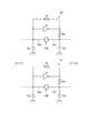
図4は、一対の加速度検出素子を含む発振回路の回路図である。なお、説明の便宜上、回路図中の該当箇所に第1配線パターン10c,10d及び第2配線パターン10e,10fの符号を付してある。
図4に示すように、発振回路50,51は、双音叉型圧電振動素子の一般的な発振回路であって、それぞれ加速度検出素子13A,13Bと、インバーターIvと、帰還抵抗Rfと、ドレイン抵抗Rdと、ゲート容量Cgと、ドレイン容量Cdと、を備えている。
この構成により、加速度検出素子13A,13Bは、加速度が印加されていない状態において、所定の共振周波数(例えば、約32kHz)で発振している。
The above will be described in detail with reference to the drawings.
FIG. 4 is a circuit diagram of an oscillation circuit including a pair of acceleration detection elements. For convenience of explanation, reference numerals of the first wiring patterns 10c and 10d and the second wiring patterns 10e and 10f are attached to the corresponding portions in the circuit diagram.
As shown in FIG. 4, the oscillation circuits 50 and 51 are general oscillation circuits of a double tuning fork type piezoelectric vibration element, and are acceleration detection elements 13A and 13B, an inverter Iv, a feedback resistor Rf, and a drain resistance, respectively. Rd, gate capacitance Cg, and drain capacitance Cd are provided.
With this configuration, the acceleration detection elements 13A and 13B oscillate at a predetermined resonance frequency (for example, about 32 kHz) in a state where no acceleration is applied.

ここで、平面視において、第1配線パターン10dと第2配線パターン10eとが重なり、第1配線パターン10cと第2配線パターン10fとが重なっていると仮定すると、電気結合作用により、第1配線パターン10dと第2配線パターン10eとの間には、静電容量C1が発生し、第1配線パターン10cと第2配線パターン10fとの間には、静電容量C2が発生する。
静電容量C0は、次式(1)で表すことができる。
C0=E×S/D…………(1)
ここで、Eは誘電率、Sは対向する電極面積、Dは電極間の距離を表す。
式(1)から、静電容量C0は、電極間の距離に反比例することが分かる。そうすると、加速度検出器1は、ベース部10、支持部14の厚さが、例えば、100〜200μm程度であり、数百μm〜数mm程度の厚さの一般的な回路基板などと比較して、静電容量C0が大きくなる傾向にあるといえる。
Here, in a plan view, assuming that the first wiring pattern 10d and the second wiring pattern 10e overlap, and the first wiring pattern 10c and the second wiring pattern 10f overlap, the first wiring pattern is caused by the electrical coupling action. A capacitance C1 is generated between the pattern 10d and the second wiring pattern 10e, and a capacitance C2 is generated between the first wiring pattern 10c and the second wiring pattern 10f.
The capacitance C0 can be expressed by the following formula (1).
C0 = E x S / D (1)
Here, E is the dielectric constant, S is the area of the opposing electrodes, and D is the distance between the electrodes.
From equation (1), it can be seen that the capacitance C0 is inversely proportional to the distance between the electrodes. Then, the acceleration detector 1 has a thickness of the base portion 10 and the support portion 14 of, for example, about 100 to 200 μm, as compared with a general circuit board having a thickness of about several hundred μm to several mm. It can be said that the capacitance C0 tends to increase.

加速度検出素子13A,13Bは、発振回路50,51に静電容量C1,C2が付加されることにより、例えば、本来の共振周波数と異なる共振周波数で発振したり、共振周波数がふらついたり、共振周波数が突然大きく変化したりする異常発振によって、誤動作する虞がある。
加えて、加速度検出素子13A,13Bは、この異常発振によって、互いに機械的にも干渉し合い、異常発振を増大させる虞がある。
The acceleration detection elements 13A and 13B are oscillated at a resonance frequency different from the original resonance frequency, or the resonance frequency fluctuates, for example, by adding capacitances C1 and C2 to the oscillation circuits 50 and 51. May malfunction due to abnormal oscillation that suddenly changes greatly.
In addition, the acceleration detecting elements 13A and 13B may interfere with each other mechanically due to the abnormal oscillation, and increase the abnormal oscillation.

このような不具合を避けるため、本実施形態の加速度検出器1では、平面視において、第1配線パターン10dと第2配線パターン10eとが重ならず、第1配線パターン10cと第2配線パターン10fとが重ならないように配置されている。
この結果、加速度検出器1では、静電容量C1,C2を無視できるレベルまで低減することが可能である。
なお、静電容量C1,C2を更に低減するためには、引き出し電極13h,13iと第1配線パターン10c,10d及び第2配線パターン10e,10fとの接続に、導電性接着剤18に代えて、金属ワイヤーを用いることが好ましい。
これによれば、加速度検出器1は、導電性接着剤18のような塗布時の広がりがなく、第1配線パターン10c,10d側と第2配線パターン10e,10f側との対向する電極面積(S)を減らすことができ、静電容量C1,C2を更に低減することが可能となる。
In order to avoid such a problem, in the acceleration detector 1 of the present embodiment, the first wiring pattern 10d and the second wiring pattern 10e do not overlap in plan view, and the first wiring pattern 10c and the second wiring pattern 10f are not overlapped. It is arranged so that and do not overlap.
As a result, in the acceleration detector 1, the capacitances C1 and C2 can be reduced to a level that can be ignored.
In order to further reduce the capacitances C1 and C2, instead of the conductive adhesive 18, the connection between the lead electrodes 13h and 13i and the first wiring patterns 10c and 10d and the second wiring patterns 10e and 10f is used. It is preferable to use a metal wire.
According to this, the acceleration detector 1 does not have a spread at the time of application like the conductive adhesive 18, and the electrode areas facing the first wiring patterns 10 c and 10 d side and the second wiring patterns 10 e and 10 f side ( S) can be reduced, and the capacitances C1 and C2 can be further reduced.

また、加速度検出器1は、ベース部10から可動部12に沿って延びる部位を有した支持部14を備え、第1配線パターン10c,10d及び第2配線パターン10e,10fが、支持部14に延在し、平面視において、互いに重ならないように配置されている。
この結果、加速度検出器1は、一方の電気信号と他方の電気信号との電気結合を抑制しつつ、支持部14によって安定した姿勢で外部部材に支持(固定)され、且つ外部部材の端子と確実に導通をとる(電気的に接続される)ことができる。
Further, the acceleration detector 1 includes a support portion 14 having a portion extending from the base portion 10 along the movable portion 12, and the first wiring patterns 10 c and 10 d and the second wiring patterns 10 e and 10 f are provided on the support portion 14. It extends and is arranged so as not to overlap each other in plan view.
As a result, the acceleration detector 1 is supported (fixed) on the external member in a stable posture by the support portion 14 while suppressing electrical coupling between one electrical signal and the other electrical signal, and the terminal of the external member Conduction can be reliably established (electrically connected).

また、加速度検出器1は、支持部14が平面視において、ベース部10とによって可動部12を囲む略矩形の枠状に形成されている。
この結果、加速度検出器1は、一方の電気信号と他方の電気信号との電気結合を抑制しつつ、枠状でない場合と比較して剛性が向上した支持部14によって、更に安定した姿勢で外部部材に支持され、且つ外部部材の端子と確実に導通をとることができる。
In the acceleration detector 1, the support portion 14 is formed in a substantially rectangular frame shape surrounding the movable portion 12 with the base portion 10 in plan view.
As a result, the acceleration detector 1 suppresses the electrical coupling between the one electric signal and the other electric signal, and further improves the rigidity of the acceleration detector 1 with the support portion 14 having improved rigidity as compared with the case where it is not frame-shaped. It is supported by the member and can be reliably connected to the terminal of the external member.

また、加速度検出器1は、加速度検出素子13A,13Bが少なくとも一以上の振動梁を有する加速度検出部13eと、加速度検出部13eの両端に接続された一対の基部13f,13gと、を備え、一方の基部13fが可動部12に固定され、他方の基部13gがベース部10に固定されている。
この結果、本構成の加速度検出器1は、一方の電気信号と他方の電気信号との電気結合を抑制しつつ、加速度検出素子13A,13Bに、例えば、構成がシンプルで検出特性に優れた双音叉型圧電振動素子などを採用可能なことから、検出特性に優れた加速度検出器を提供することができる。
The acceleration detector 1 includes an acceleration detection unit 13e in which the acceleration detection elements 13A and 13B have at least one vibration beam, and a pair of bases 13f and 13g connected to both ends of the acceleration detection unit 13e. One base portion 13 f is fixed to the movable portion 12, and the other base portion 13 g is fixed to the base portion 10.
As a result, the acceleration detector 1 of this configuration suppresses the electrical coupling between one electrical signal and the other electrical signal, while the acceleration detection elements 13A and 13B have, for example, a dual configuration with a simple configuration and excellent detection characteristics. Since a tuning fork type piezoelectric vibration element or the like can be employed, an acceleration detector having excellent detection characteristics can be provided.

また、加速度検出器1は、可動部12の両主面12a,12bに、平面視において、一部が支持部14と重なる質量部15が配置され、可動部12がZ軸方向に加わる加速度(+α、−α)に応じて継ぎ手部11を支点にしてZ軸方向に変位可能であり、質量部15と支持部14とが重なる領域Bにおける質量部15と支持部14との間に隙間Cが設けられている。
このことから、加速度検出器1は、加速度に応じてZ軸方向に変位する可動部12の変位を、可動部12の両主面12a,12bに固定された質量部15が隙間C分変位して支持部14と接触することによって、所定の範囲内に規制することができる。
Further, in the acceleration detector 1, a mass portion 15 that partially overlaps the support portion 14 in a plan view is disposed on both the main surfaces 12 a and 12 b of the movable portion 12, and the acceleration that the movable portion 12 applies in the Z-axis direction ( + Α, −α), which can be displaced in the Z-axis direction with the joint portion 11 as a fulcrum, and a gap C between the mass portion 15 and the support portion 14 in a region B where the mass portion 15 and the support portion 14 overlap. Is provided.
From this, the acceleration detector 1 causes the displacement of the movable portion 12 that is displaced in the Z-axis direction according to the acceleration, and the mass portion 15 fixed to both the main surfaces 12a and 12b of the movable portion 12 is displaced by the gap C. Then, the contact with the support portion 14 can be regulated within a predetermined range.

この結果、加速度検出器1は、自身に可動部12の変位を規制するストッパーを設けたことから、例えば、外部部材であるパッケージに依存することなく可動部12の変位を自身で規制することが可能となる。
したがって、加速度検出器1は、例えば、外部部材であるパッケージの内面と加速度検出器1との隙間を、質量部15と支持部14との隙間Cよりも十分に大きく設定することが可能となり、パッケージの内面との衝突や強度の限界を超える変位による、可動部12や加速度検出素子13A,13Bの破損を回避することができる。
As a result, since the acceleration detector 1 is provided with a stopper that restricts the displacement of the movable portion 12, for example, the acceleration detector 1 can regulate the displacement of the movable portion 12 without depending on a package that is an external member. It becomes possible.
Therefore, for example, the acceleration detector 1 can set the gap between the inner surface of the package as an external member and the acceleration detector 1 to be sufficiently larger than the gap C between the mass portion 15 and the support portion 14. It is possible to avoid damage to the movable portion 12 and the acceleration detection elements 13A and 13B due to collision with the inner surface of the package or displacement exceeding the limit of strength.

また、加速度検出器1は、自身に可動部12の変位を規制するストッパーを設けたことから、可動部12の変位の規制具合を、例えば、パッケージなどの外部部材に収容する前に確認することができる。
これにより、加速度検出器1は、良品率が格段に向上し、実使用時における破損などの不具合を低減することができる。
In addition, since the acceleration detector 1 is provided with a stopper for restricting the displacement of the movable portion 12, the acceleration detector 1 confirms the degree of restriction of the displacement of the movable portion 12 before being accommodated in an external member such as a package, for example. Can do.
Thereby, the acceleration detector 1 can remarkably improve the yield rate, and can reduce problems such as breakage during actual use.

また、加速度検出器1は、平面視において、支持部14がベース部10とによって可動部12を囲む略矩形の枠状に形成されていることから、例えば、後述する変形例のような、支持部14が可動部12の両側に分割されている場合と比較して、支持部14における質量部15の接触時(衝突時)の強度(耐衝撃性)を向上させることができる。   Further, since the acceleration detector 1 is formed in a substantially rectangular frame shape surrounding the movable portion 12 with the base portion 10 in a plan view, the acceleration detector 1 is supported, for example, as in a modification described later. Compared with the case where the portion 14 is divided on both sides of the movable portion 12, the strength (impact resistance) of the support portion 14 when the mass portion 15 is in contact (collision) can be improved.

また、加速度検出器1は、質量部15が可動部12の一方の主面12a(他方の主面12b)側に突出する凸部15aを有し、凸部15aの先端部が可動部12の一方の主面12a及び他方の主面12bに接合材16を介して接合されている。
これにより、加速度検出器1は、例えば、凸部15aのない質量部15が接合材16で可動部12の両主面12a,12bに広範囲に亘って接着されている構成と比較して、質量部15の接合範囲を狭くできることから、周囲の温度変化に起因する熱応力に伴う可動部12の歪みを抑制することができる。
この結果、加速度検出器1は、上記歪みに起因する応力が低減され、加速度検出精度や温度特性などの加速度検出特性を向上させることができる。
Further, the acceleration detector 1 has a convex portion 15 a in which the mass portion 15 protrudes toward the one main surface 12 a (the other main surface 12 b) of the movable portion 12, and the tip portion of the convex portion 15 a is the movable portion 12. The main surface 12a and the other main surface 12b are joined via a joining material 16.
Thereby, the acceleration detector 1 has a mass compared with a configuration in which, for example, the mass portion 15 without the convex portion 15a is bonded to both the main surfaces 12a and 12b of the movable portion 12 with the bonding material 16 over a wide range. Since the joining range of the part 15 can be narrowed, the distortion of the movable part 12 due to the thermal stress caused by the ambient temperature change can be suppressed.
As a result, the acceleration detector 1 can reduce the stress caused by the distortion, and can improve acceleration detection characteristics such as acceleration detection accuracy and temperature characteristics.

また、加速度検出器1は、接合材16がシリコーン系樹脂を含む接着剤としてのシリコーン系熱硬化型接着剤であることから、シリコーン系樹脂特有の弾性により質量部15と支持部14との接触時(衝突時)の衝撃力を緩和及び吸収することができる。
この結果、加速度検出器1は、質量部15と支持部14との接触時の損傷を低減することができ、耐衝撃性能を向上させることが可能となる。
Further, in the acceleration detector 1, since the bonding material 16 is a silicone thermosetting adhesive as an adhesive containing a silicone resin, the mass portion 15 and the support portion 14 are brought into contact with each other due to the elasticity unique to the silicone resin. The impact force at the time (collision) can be relaxed and absorbed.
As a result, the acceleration detector 1 can reduce damage at the time of contact between the mass portion 15 and the support portion 14, and can improve the impact resistance performance.

なお、加速度検出器1は、耐衝撃性能に支障がなければ、平面視において、質量部15と支持部14とを重ねなくてもよい(ストッパーを除去してもよい)。
また、加速度検出器1は、質量部15における接着箇所の位置ズレ、接着範囲の想定外の広がり、接着高さ(隙間C)のばらつきなどが殆どないと考えられる場合には、質量部15に凸部15aを設けなくてもよい。
The acceleration detector 1 may not overlap the mass portion 15 and the support portion 14 in plan view (the stopper may be removed) as long as the impact resistance performance is not hindered.
In addition, the acceleration detector 1 may be arranged in the mass portion 15 in the case where it is considered that there is almost no positional deviation of the adhesion portion in the mass portion 15, an unexpected spread of the adhesion range, and a variation in adhesion height (gap C). The convex portion 15a may not be provided.

(変形例)
次に、第1実施形態の変形例について説明する。
図5は、第1実施形態の変形例の加速度検出器の概略構成を示す模式平断面図である。図5(a)は、平面図、図5(b)は、図5(a)のD−D線での断面図、図5(c)は、図5(a)のE−E線での断面図である。なお、一部の配線は省略してあり、各構成要素の寸法比率は実際と異なる。
また、上記第1実施形態との共通部分には、同一符号を付して詳細な説明を省略し、上記第1実施形態と異なる部分を中心に説明する。
(Modification)
Next, a modification of the first embodiment will be described.
FIG. 5 is a schematic plan sectional view showing a schematic configuration of an acceleration detector according to a modification of the first embodiment. 5A is a plan view, FIG. 5B is a cross-sectional view taken along the line DD in FIG. 5A, and FIG. 5C is a cross-sectional view taken along the line EE in FIG. FIG. In addition, some wiring is abbreviate | omitted and the dimensional ratio of each component differs from actual.
Also, common parts with the first embodiment will be denoted by the same reference numerals, detailed description thereof will be omitted, and different parts from the first embodiment will be mainly described.

図5に示すように、加速度検出器2は、支持部114における可動部112の自由端側(−Y側)の、第1実施形態ではX軸方向に延びて繋がっていた部分が、Y軸方向からX軸方向に屈曲した根元部分を残して切り取られ、支持部114が可動部112の+X側と−X側との2つに分割されている。
また、加速度検出器2は、支持部114の切り取られたスペースに可動部112の自由端側が延在している。
As shown in FIG. 5, in the acceleration detector 2, the portion on the free end side (−Y side) of the movable portion 112 in the support portion 114 that extends and is connected in the X-axis direction in the first embodiment is the Y-axis. The support part 114 is divided into two parts, that is, the + X side and the −X side of the movable part 112, leaving a root portion bent in the X-axis direction from the direction.
Further, in the acceleration detector 2, the free end side of the movable portion 112 extends in the space where the support portion 114 is cut out.

加速度検出器2は、可動部112の上記延在した部分に加速度検出素子113A,113Bが配置可能なように、質量部115が+X側と−X側との2つにそれぞれ分割されている。そして、2つに分割された質量部115が、加速度検出素子113A,113Bを+X側と−X側とから挟むように配置されている。
質量部115は、可動部112の一方の主面112a(他方の主面112b)側に突出する円柱状(円板状)の凸部115aを有し、凸部115aの先端部が、可動部112の一方の主面112a及び他方の主面112bに接合材16を介して接合されている。
In the acceleration detector 2, the mass part 115 is divided into two parts, a + X side and a −X side, so that the acceleration detection elements 113 </ b> A and 113 </ b> B can be arranged in the extended part of the movable part 112. The mass section 115 divided into two is arranged so as to sandwich the acceleration detection elements 113A and 113B from the + X side and the −X side.
The mass portion 115 has a columnar (disc-shaped) convex portion 115a that protrudes toward the one main surface 112a (the other main surface 112b) of the movable portion 112, and the tip of the convex portion 115a is a movable portion. 112 is bonded to one main surface 112 a and the other main surface 112 b via a bonding material 16.

質量部115の一部は、平面視において、支持部114における可動部112の自由端側のY軸方向からX軸方向に屈曲した部分(先端部分)と重なっている(図5(a)のハッチング部分、領域B)。
質量部115と支持部114とが重なる領域Bでは、図5(c)に示すように、質量部115と支持部114との間に隙間Cが設けられている。
なお、加速度検出器2の動作については、第1実施形態に準じるので説明を省略する。
A part of the mass portion 115 overlaps with a portion (tip portion) bent in the X-axis direction from the Y-axis direction on the free end side of the movable portion 112 in the support portion 114 in plan view (see FIG. 5A). Hatched portion, region B).
In the region B where the mass portion 115 and the support portion 114 overlap, a gap C is provided between the mass portion 115 and the support portion 114 as shown in FIG.
Note that the operation of the acceleration detector 2 is the same as in the first embodiment, and a description thereof will be omitted.

上記構成により、加速度検出器2は、加速度検出素子113A,113Bの一方の基部13fを可動部112の自由端側の端部に移動させ、他方の基部13gを第1実施形態と同じ位置に配置することができる。
このことから、加速度検出器2は、第1実施形態と比較して、Y軸方向のサイズを大きくすることなく、加速度検出素子113A,113Bの加速度検出部113eの振動梁113c,113dを第1実施形態よりも長くすることが可能となる。
With the above configuration, the acceleration detector 2 moves one base portion 13f of the acceleration detection elements 113A and 113B to the end portion on the free end side of the movable portion 112, and arranges the other base portion 13g at the same position as in the first embodiment. can do.
From this, the acceleration detector 2 does not increase the size in the Y-axis direction as compared with the first embodiment, and the vibration beams 113c and 113d of the acceleration detection unit 113e of the acceleration detection elements 113A and 113B are the first. It becomes possible to make it longer than the embodiment.

上述したように、変形例の加速度検出器2は、第1実施形態と比較して、Y軸方向のサイズを大きくすることなく、加速度検出素子113A,113Bの振動梁113c,113dを第1実施形態よりも長くすることが可能なことから、加速度による可動部112の僅かな変位でも振動梁113c,113dが伸縮しやすくなり、周波数差の変化が発生しやすくなる。
この結果、加速度検出器2は、第1実施形態と比較して、Y軸方向のサイズを大きくすることなく、加速度の検出感度を向上させることができる。
As described above, the acceleration detector 2 according to the modified example includes the vibrating beams 113c and 113d of the acceleration detection elements 113A and 113B in the first embodiment without increasing the size in the Y-axis direction as compared with the first embodiment. Since it can be made longer than the shape, the vibration beams 113c and 113d are easily expanded and contracted even with a slight displacement of the movable portion 112 due to acceleration, and a change in frequency difference is likely to occur.
As a result, the acceleration detector 2 can improve the acceleration detection sensitivity without increasing the size in the Y-axis direction as compared with the first embodiment.

なお、加速度検出器2は、第1実施形態と同様に、耐衝撃性能に支障がなければ、平面視において、質量部115と支持部114とを重ねなくてもよい(ストッパーを除去してもよい)。
また、加速度検出器2は、質量部115における接着箇所の位置ズレ、接着範囲の想定外の広がり、接着高さ(隙間C)のばらつきなどが殆どないと考えられる場合には、質量部115に凸部115aを設けなくてもよい。
As in the first embodiment, the acceleration detector 2 does not have to overlap the mass portion 115 and the support portion 114 in plan view as long as the impact resistance performance is not hindered (even if the stopper is removed). Good).
In addition, the acceleration detector 2 may be connected to the mass portion 115 when it is considered that there is almost no misalignment of the adhesion portion in the mass portion 115, an unexpected expansion of the adhesion range, or a variation in adhesion height (gap C). The convex 115a may not be provided.

(第2実施形態)
次に、上記第1実施形態及び変形例で述べた加速度検出器を備えた加速度検出デバイスについて説明する。
図6は、第2実施形態の加速度検出デバイスの概略構成を示す模式平断面図である。図6(a)は、リッド(蓋体)側から俯瞰した平面図であり、図6(b)は、図6(a)のF−F線での断面図である。なお、平面図では、リッドを省略してある。また、一部の配線は省略してある。
なお、上記第1実施形態との共通部分には、同一符号を付して詳細な説明を省略し、上記第1実施形態と異なる部分を中心に説明する。
(Second Embodiment)
Next, an acceleration detection device including the acceleration detector described in the first embodiment and the modification will be described.
FIG. 6 is a schematic plan sectional view showing a schematic configuration of the acceleration detection device of the second embodiment. 6A is a plan view seen from the lid (lid body) side, and FIG. 6B is a cross-sectional view taken along line FF in FIG. 6A. In the plan view, the lid is omitted. Some wiring is omitted.
In addition, the same code | symbol is attached | subjected to a common part with the said 1st Embodiment, detailed description is abbreviate | omitted, and it demonstrates centering on a different part from the said 1st Embodiment.

図6に示すように、加速度検出デバイス3は、上記第1実施形態で述べた加速度検出器1と、加速度検出器1を収容するパッケージ20と、を備えている。
パッケージ20は、平面形状が略矩形で凹部を有したパッケージベース21と、パッケージベース21の凹部を覆う平面形状が略矩形で平板状のリッド22と、を有し、略直方体形状に形成されている。
パッケージベース21には、セラミックグリーンシートを成形して積層し焼成した酸化アルミニウム質焼結体、水晶、ガラス、シリコンなどが用いられている。
リッド22には、パッケージベース21と同材料、または、コバール、42アロイ、ステンレス鋼などの金属が用いられている。
As shown in FIG. 6, the acceleration detection device 3 includes the acceleration detector 1 described in the first embodiment and a package 20 that houses the acceleration detector 1.
The package 20 includes a package base 21 having a substantially rectangular planar shape and a recess, and a lid 22 having a substantially rectangular planar shape covering the recess of the package base 21 and is formed in a substantially rectangular parallelepiped shape. Yes.
The package base 21 is made of an aluminum oxide sintered body, crystal, glass, silicon, or the like formed by laminating and firing ceramic green sheets.
The lid 22 is made of the same material as the package base 21 or a metal such as Kovar, 42 alloy, or stainless steel.

パッケージベース21には、内底面(凹部の内側の底面)23の外周部分から凹部の内壁に沿って突出した対向する2箇所の段差部23aに、内部端子24a,24b,25a,25bが設けられている。
内部端子24a,24b,25a,25bは、各段差部23aの長手方向の両端であって、加速度検出器1の支持部14に延在する第1配線パターン10c,10d及び第2配線パターン10e,10fの導通部分と対向する位置(平面視において重なる位置)に設けられている。
The package base 21 is provided with internal terminals 24a, 24b, 25a, and 25b at two opposing step portions 23a that protrude from the outer peripheral portion of the inner bottom surface (the bottom surface inside the recess) 23 along the inner wall of the recess. ing.
The internal terminals 24a, 24b, 25a, 25b are the first wiring patterns 10c, 10d and the second wiring patterns 10e, which extend at the longitudinal ends of the step portions 23a and extend to the support portion 14 of the acceleration detector 1. It is provided at a position (a position overlapping in plan view) that faces the conductive portion 10f.

パッケージベース21の外底面(内底面23の反対側の面、外側の底面)26には、電子機器などの外部部材に実装される際に用いられる外部端子27a,27b,28a,28bが形成されている。
外部端子27a,27b,28a,28bは、図示しない内部配線によって内部端子24a,24b,25a,25bと接続されている。例えば、外部端子27aは、内部端子24aと接続され、外部端子27bは、内部端子24bと接続され、外部端子28aは、内部端子25aと接続され、外部端子28bは、内部端子25bと接続されている。
内部端子24a,24b,25a,25b及び外部端子27a,27b,28a,28bは、W、Moなどのメタライズ層にNi、Auなどの各被膜をメッキなどの方法により積層した金属膜からなる。
External terminals 27a, 27b, 28a, and 28b used for mounting on an external member such as an electronic device are formed on the outer bottom surface (the surface opposite to the inner bottom surface 23, the outer bottom surface) 26 of the package base 21. ing.
The external terminals 27a, 27b, 28a, 28b are connected to the internal terminals 24a, 24b, 25a, 25b by internal wiring (not shown). For example, the external terminal 27a is connected to the internal terminal 24a, the external terminal 27b is connected to the internal terminal 24b, the external terminal 28a is connected to the internal terminal 25a, and the external terminal 28b is connected to the internal terminal 25b. Yes.
The internal terminals 24a, 24b, 25a, 25b and the external terminals 27a, 27b, 28a, 28b are made of a metal film obtained by laminating each film such as Ni or Au on a metallized layer such as W or Mo by a method such as plating.

パッケージベース21には、凹部の底部にパッケージ20の内部を封止する封止部29が設けられている。
封止部29は、パッケージベース21に形成された、外底面26側の孔径が内底面23側の孔径より大きい段付きの貫通孔29aに、Au/Ge合金、ハンダなどからなる封止材29bを投入し、加熱溶融後、固化させることでパッケージ20の内部を気密に封止する構成となっている。
The package base 21 is provided with a sealing portion 29 that seals the inside of the package 20 at the bottom of the recess.
The sealing portion 29 is formed in a stepped through hole 29a formed in the package base 21 and having a hole diameter on the outer bottom surface 26 side larger than that on the inner bottom surface 23 side, and a sealing material 29b made of Au / Ge alloy, solder, or the like. The inside of the package 20 is hermetically sealed by charging and solidifying after heating and melting.

加速度検出デバイス3は、加速度検出器1の支持部14に延在する第1配線パターン10c,10d及び第2配線パターン10e,10fの導通部分が、例えば、金属フィラーなどの導電性物質が混合された導電性接着剤(例えば、シリコーン系導電性接着剤)30を介して、パッケージベース21の段差部23aの内部端子24a,24b,25a,25bに固定されている。
これにより、第1配線パターン10c,10d及び第2配線パターン10e,10fは、内部端子24a,24b,25a,25bと導通をとることができる(電気的に接続される)。
In the acceleration detection device 3, the conductive portions of the first wiring patterns 10c and 10d and the second wiring patterns 10e and 10f extending to the support portion 14 of the acceleration detector 1 are mixed with a conductive material such as a metal filler, for example. The conductive adhesive (for example, silicone-based conductive adhesive) 30 is fixed to the internal terminals 24a, 24b, 25a, and 25b of the step portion 23a of the package base 21.
Thus, the first wiring patterns 10c and 10d and the second wiring patterns 10e and 10f can be electrically connected (electrically connected) to the internal terminals 24a, 24b, 25a, and 25b.

加速度検出デバイス3は、加速度検出器1がパッケージベース21の内部端子24a,24b,25a,25bに固定された状態で、パッケージベース21の凹部がリッド22により覆われ、パッケージベース21とリッド22とがシームリング、低融点ガラス、接着剤などの接合部材22aで接合される。
加速度検出デバイス3は、リッド22の接合後、パッケージ20の内部が減圧された状態(真空度の高い状態)で、封止部29の貫通孔29aに封止材29bが投入され、加熱溶融後、固化されることにより、パッケージ20の内部が気密に封止される。
なお、パッケージ20の内部は、窒素、ヘリウム、アルゴンなどの不活性ガスが充填されていてもよい。
なお、パッケージは、パッケージベース及びリッドの両方に凹部を有していてもよい。
In the acceleration detection device 3, the recess of the package base 21 is covered with the lid 22 in a state where the acceleration detector 1 is fixed to the internal terminals 24 a, 24 b, 25 a, and 25 b of the package base 21, and the package base 21, the lid 22, Are joined by a joining member 22a such as a seam ring, a low-melting glass, or an adhesive.
In the acceleration detecting device 3, after the lid 22 is joined, the sealing material 29b is put into the through hole 29a of the sealing portion 29 in a state where the inside of the package 20 is decompressed (high vacuum state), and after heating and melting By solidifying, the inside of the package 20 is hermetically sealed.
Note that the inside of the package 20 may be filled with an inert gas such as nitrogen, helium, or argon.
The package may have a recess in both the package base and the lid.

加速度検出デバイス3は、外部端子27a,27b,28a,28b、内部端子24a,24b,25a,25b、第1配線パターン10c,10d及び第2配線パターン10e,10fなどを経由して加速度検出器1の励振電極に印加される駆動信号によって、加速度検出器1の加速度検出素子13A,13Bのそれぞれの振動梁13c,13dが所定の周波数で発振(共振)する。
そして、加速度検出デバイス3は、加わる加速度に応じて変化する加速度検出器1の加速度検出素子13A,13Bのそれぞれの共振周波数を出力信号として出力する。
The acceleration detection device 3 includes the acceleration detector 1 via the external terminals 27a, 27b, 28a, 28b, the internal terminals 24a, 24b, 25a, 25b, the first wiring patterns 10c, 10d and the second wiring patterns 10e, 10f. The vibration beams 13c and 13d of the acceleration detection elements 13A and 13B of the acceleration detector 1 oscillate (resonate) at a predetermined frequency by the drive signal applied to the excitation electrodes.
And the acceleration detection device 3 outputs each resonance frequency of the acceleration detection elements 13A and 13B of the acceleration detector 1 which changes according to the applied acceleration as an output signal.

上述したように、第2実施形態の加速度検出デバイス3は、加速度検出器1を備えたことから、上記第1実施形態に記載された効果を奏する加速度検出デバイス(例えば、電気結合に起因する加速度検出素子13A,13Bの異常発振による誤動作を回避し、印加される加速度の誤検出や検出精度の低下などの不具合の発生を低減することができる加速度検出デバイス)を提供することができる。
なお、加速度検出デバイス3は、加速度検出器1に代えて加速度検出器2を備えた場合においても、上記と同様の効果及び加速度検出器2の特有の効果を奏する加速度検出デバイスを提供することができる。
As described above, since the acceleration detection device 3 of the second embodiment includes the acceleration detector 1, the acceleration detection device that exhibits the effect described in the first embodiment (for example, acceleration caused by electrical coupling). It is possible to provide an acceleration detection device that can avoid malfunction due to abnormal oscillation of the detection elements 13A and 13B and reduce occurrence of problems such as erroneous detection of applied acceleration and a decrease in detection accuracy.
Note that the acceleration detection device 3 can provide an acceleration detection device that exhibits the same effects as described above and the unique effects of the acceleration detector 2 even when the acceleration detector 2 is provided instead of the acceleration detector 1. it can.

(第3実施形態)
次に、上記実施形態及び変形例で述べた加速度検出器を備えた電子機器としての傾斜計について説明する。
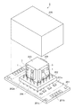
図7は、第3実施形態の傾斜計を示す模式斜視図である。図8は、傾斜計の内部に収容された傾斜センサーモジュールの概略構成を示す部分展開模式斜視図である。
図7、図8に示すように、傾斜計4は、上記第1実施形態で述べた加速度検出器1を、傾斜センサーモジュール5の傾斜センサーとして備えている。
図8に示すように、傾斜センサーモジュール5は、ベース基板201と、断熱基板202と、基台203と、加速度検出器1を備えた加速度検出デバイス3と、発振器204と、キャップ205と、を備え、傾斜計4の内部に収容されている。
(Third embodiment)
Next, an inclinometer as an electronic apparatus provided with the acceleration detector described in the embodiment and the modification will be described.
FIG. 7 is a schematic perspective view showing the inclinometer of the third embodiment. FIG. 8 is a partially developed schematic perspective view showing a schematic configuration of the tilt sensor module housed in the inclinometer.
As shown in FIGS. 7 and 8, the inclinometer 4 includes the acceleration detector 1 described in the first embodiment as a tilt sensor of the tilt sensor module 5.
As shown in FIG. 8, the inclination sensor module 5 includes a base substrate 201, a heat insulating substrate 202, a base 203, an acceleration detection device 3 including the acceleration detector 1, an oscillator 204, and a cap 205. And is accommodated inside the inclinometer 4.

矩形平板状のベース基板201には、例えば、FR−4(ガラス布入りエポキシ樹脂基板)が用いられ、搭載された回路素子201aによって、加速度検出デバイス3や発振器204に関わる周辺回路が構成されている。また、ベース基板201には、外部(傾斜計本体)との入出力のための端子201bや、傾斜計本体への取り付け孔201cが形成されている。
矩形平板状の断熱基板202は、PBT(ポリブチレンテレフタレート)、LCP(液晶ポリマー)などの低熱伝導率で耐熱性、電気特性、寸法安定性などに優れた樹脂が用いられ、厚み方向に貫通して固定されている細いピン状(棒状)の複数の接続ピン202aによって、ベース基板201に隙間を有して接続されている。
基台203は、アルミニウム、アルミニウム合金、銅、銅合金などの金属を用いて、削り出しまたは板金加工により略直方体形状に形成され、断熱基板202に、例えば、接着剤などで固定されている。なお、基台203には、上記の樹脂や酸化アルミニウム質焼結体(セラミック類)などを用いてもよい。
For example, FR-4 (epoxy resin substrate with glass cloth) is used for the rectangular flat base substrate 201, and peripheral circuits related to the acceleration detection device 3 and the oscillator 204 are configured by the mounted circuit elements 201a. Yes. Further, the base substrate 201 is formed with a terminal 201b for input / output with the outside (inclinometer body) and a mounting hole 201c to the inclinometer body.
The rectangular flat heat insulating substrate 202 is made of a resin having a low thermal conductivity such as PBT (polybutylene terephthalate) or LCP (liquid crystal polymer) and having excellent heat resistance, electrical characteristics, dimensional stability, etc., and penetrates in the thickness direction. A plurality of thin pin-shaped (pin-shaped) connection pins 202 a are connected to the base substrate 201 with a gap.
The base 203 is formed into a substantially rectangular parallelepiped shape by cutting or sheet metal processing using a metal such as aluminum, aluminum alloy, copper, or copper alloy, and is fixed to the heat insulating substrate 202 with, for example, an adhesive. The base 203 may be made of the above resin or aluminum oxide sintered body (ceramics).

加速度検出デバイス3及び発振器204は、基台203の側面(断熱基板202に対して直立する面)に、例えば、導電性接着剤などによって固定されている。2つの加速度検出デバイス3は、基台203における隣り合う直角に接続された側面にそれぞれ固定されている。これにより、傾斜センサーモジュール5は、互いに直交する2軸に対する傾斜を検出することができる。
発振器204は、基台203における一方の加速度検出デバイス3が固定された側面と対向する側面(換言すれば、他方の加速度検出デバイス3が固定された側面と隣り合う側面)に固定されている。
加速度検出デバイス3及び発振器204は、リード線206によって断熱基板202の接続ピン202aに接続され、接続ピン202aを経由してベース基板201に接続されている。
The acceleration detection device 3 and the oscillator 204 are fixed to the side surface of the base 203 (the surface standing upright with respect to the heat insulating substrate 202) with, for example, a conductive adhesive. The two acceleration detection devices 3 are respectively fixed to side surfaces of the base 203 that are connected at right angles to each other. Thereby, the inclination sensor module 5 can detect the inclination with respect to two axes orthogonal to each other.
The oscillator 204 is fixed to the side surface of the base 203 that faces the side surface to which one acceleration detection device 3 is fixed (in other words, the side surface adjacent to the side surface to which the other acceleration detection device 3 is fixed).
The acceleration detection device 3 and the oscillator 204 are connected to the connection pins 202a of the heat insulating substrate 202 by lead wires 206, and are connected to the base substrate 201 via the connection pins 202a.

なお、一方の加速度検出デバイス3の近傍には、周辺の温度を検知するサーミスター207(温度センサー)が備えられている。サーミスター207は、周辺の温度を検知して、加速度検出デバイス3及び発振器204の周波数特性の温度補償(温度補正)をする際の、温度検知手段として備えられている。
サーミスター207は、上記加速度検出デバイス3及び発振器204と同様に、リード線206によって断熱基板202の接続ピン202aに接続され、接続ピン202aを経由してベース基板201に接続されている。
発振器204は、加速度検出時における加速度検出デバイス3(加速度検出器1)の共振周波数と比較する比較回路の基準周波数(基準共振周波数)発振源として備えられている。
A thermistor 207 (temperature sensor) that detects the ambient temperature is provided in the vicinity of one acceleration detection device 3. The thermistor 207 is provided as a temperature detection means for detecting the ambient temperature and performing temperature compensation (temperature correction) of the frequency characteristics of the acceleration detection device 3 and the oscillator 204.
Similar to the acceleration detection device 3 and the oscillator 204, the thermistor 207 is connected to the connection pin 202a of the heat insulating substrate 202 by a lead wire 206, and is connected to the base substrate 201 via the connection pin 202a.
The oscillator 204 is provided as a reference frequency (reference resonance frequency) oscillation source of a comparison circuit that compares with the resonance frequency of the acceleration detection device 3 (acceleration detector 1) at the time of acceleration detection.

ベース基板201側に開口部を備えた箱状のキャップ205には、断熱基板202と同様に低熱伝導率の樹脂(PBT、ABS、PCなど)が用いられ、ベース基板201上の断熱基板202、基台203、加速度検出デバイス3、サーミスター207、発振器204、回路素子201aなどを覆うようにベース基板201に固定されている。   For the box-shaped cap 205 having an opening on the base substrate 201 side, a low thermal conductivity resin (PBT, ABS, PC, etc.) is used similarly to the heat insulating substrate 202, and the heat insulating substrate 202 on the base substrate 201, It is fixed to the base substrate 201 so as to cover the base 203, the acceleration detection device 3, the thermistor 207, the oscillator 204, the circuit element 201a, and the like.

これらの構成により、傾斜センサーモジュール5は、周囲の温度変化の加速度検出デバイス3への到達を遅延させることができる。詳述すると、ベース基板201からの接触による熱伝導は、細いピン状の接続ピン202aや低熱伝導率の樹脂が用いられた断熱基板202により遅延され、加速度検出デバイス3の周辺の大気の対流や、外部部材の放射熱(輻射熱)による熱伝導は、低熱伝導率の樹脂が用いられたキャップ205による外気及び放射熱源からの遮断によって遅延される。
このように、傾斜センサーモジュール5は、周囲の温度変化の加速度検出デバイス3への到達を遅延させることで、加速度検出デバイス3の温度変化をなだらかにすることが可能となることから、加速度検出デバイス3(加速度検出器1)の、例えば、加速度検出精度などの加速度検出特性を良好な状態に維持することができる。
With these configurations, the inclination sensor module 5 can delay the arrival of the ambient temperature change to the acceleration detection device 3. More specifically, the heat conduction due to the contact from the base substrate 201 is delayed by the thin pin-like connection pins 202a and the heat insulating substrate 202 using a low thermal conductivity resin, and the convection of the atmosphere around the acceleration detection device 3 The heat conduction by the radiant heat (radiant heat) of the external member is delayed by the shielding from the outside air and the radiant heat source by the cap 205 using a resin having a low thermal conductivity.
As described above, the inclination sensor module 5 can moderate the temperature change of the acceleration detection device 3 by delaying the arrival of the ambient temperature change to the acceleration detection device 3. 3 (acceleration detector 1), for example, acceleration detection characteristics such as acceleration detection accuracy can be maintained in a good state.

図7に戻って、傾斜計4は、例えば、山の斜面、道路の法面、盛土の擁壁面などの被計測場所に設置される。傾斜計4は、外部からケーブル40を介して電源が供給され、または電源を内蔵し、図示しない駆動回路によって傾斜センサーモジュール5(加速度検出器1)に駆動信号が送られている。
そして、傾斜計4は、図示しない検出回路によって、傾斜センサーモジュール5(加速度検出器1)に加わる重力加速度に応じて変化する各共振周波数の周波数差から、傾斜計4の姿勢の変化(傾斜計4に対する重力加速度が加わる方向の変化)を検出し、それを角度に換算して、例えば、無線またはケーブル40などで基地局にデータ転送する。これにより、傾斜計4は、日常の管理や異常の早期発見に貢献することができる。
なお、傾斜計4は、加速度検出器1に代えて加速度検出器2を傾斜センサーとして備えていてもよい。
Returning to FIG. 7, the inclinometer 4 is installed at a measurement site such as a mountain slope, a road slope, or a retaining wall of embankment. The inclinometer 4 is supplied with power from the outside via a cable 40 or has a built-in power supply, and a drive signal is sent to the tilt sensor module 5 (acceleration detector 1) by a drive circuit (not shown).
Then, the inclinometer 4 changes the attitude of the inclinometer 4 (inclinometer from the frequency difference of each resonance frequency that changes according to the gravitational acceleration applied to the inclination sensor module 5 (acceleration detector 1) by a detection circuit (not shown). Change in the direction in which gravitational acceleration is applied to 4) is detected, converted into an angle, and data is transferred to the base station, for example, by radio or cable 40. Thereby, the inclinometer 4 can contribute to daily management and early detection of abnormality.
Note that the inclinometer 4 may include the acceleration detector 2 as an inclination sensor instead of the acceleration detector 1.

上述した加速度検出器1,2は、上記傾斜計に限らず、地震計、ナビゲーション装置、姿勢制御装置、ゲームコントローラー、携帯電話などの加速度センサー、傾斜センサーなどとして好適に用いることができ、いずれの場合にも上記実施形態及び変形例で説明した効果を奏する電子機器を提供することができる。   The above-described acceleration detectors 1 and 2 are not limited to the inclinometer, and can be suitably used as an acceleration sensor such as a seismometer, a navigation device, an attitude control device, a game controller, a mobile phone, an inclination sensor, etc. Even in this case, it is possible to provide an electronic device that exhibits the effects described in the embodiment and the modification.

なお、上記各実施形態及び変形例において、ベース部、継ぎ手部、可動部、支持部の材料は、水晶に限定するものではなく、ガラス、またはシリコンなどの半導体材料であってもよい。
また、加速度検出素子の基材は、水晶に限定するものではなく、タンタル酸リチウム(LiTaO3)、四ホウ酸リチウム(Li247)、ニオブ酸リチウム(LiNbO3)、チタン酸ジルコン酸鉛(PZT)、酸化亜鉛(ZnO)、窒化アルミニウム(AlN)などの圧電材料、または酸化亜鉛(ZnO)、窒化アルミニウム(AlN)などの圧電材料を被膜として備えたシリコンなどの半導体材料であってもよい。
In each of the above embodiments and modifications, the material of the base part, the joint part, the movable part, and the support part is not limited to quartz, but may be a semiconductor material such as glass or silicon.
The substrate of the acceleration detecting element is not limited to quartz, but lithium tantalate (LiTaO 3 ), lithium tetraborate (Li 2 B 4 O 7 ), lithium niobate (LiNbO 3 ), zirconate titanate It is a semiconductor material such as silicon provided with a piezoelectric material such as lead oxide (PZT), zinc oxide (ZnO), aluminum nitride (AlN), or a piezoelectric material such as zinc oxide (ZnO) or aluminum nitride (AlN) as a film. May be.

1,2…加速度検出器、3…加速度検出デバイス、4…電子機器としての傾斜計、5…傾斜センサーモジュール、10…ベース部、10a…一方の主面、10b…他方の主面、10c,10d…第1配線パターン、10e,10f…第2配線パターン、11…継ぎ手部、11a…溝部、12…可動部、12a…一方の主面、12b…他方の主面、13A,13B…加速度検出素子、13c,13d…振動梁、13e…加速度検出部、13f,13g…基部、13h,13i…引き出し電極、14…支持部、14a…一方の主面、14b…他方の主面、14c…スルーホール、15…質量部、15a…凸部、16…接合材、17…接合部材、18…導電性接着剤、20…パッケージ、21…パッケージベース、22…リッド、22a…接合部材、23…内底面、23a…段差部、24a,24b,25a,25b…内部端子、26…外底面、27a,27b,28a,28b…外部端子、29…封止部、29a…貫通孔、29b…封止材、30…導電性接着剤、40…ケーブル、112…可動部、112a…一方の主面、112b…他方の主面、113A,113B…加速度検出素子、113c,113d…振動梁、113e…加速度検出部、114…支持部、115…質量部、115a…凸部、201…ベース基板、201a…回路素子、201b…端子、201c…取り付け孔、202…断熱基板、202a…接続ピン、203…基台、204…発振器、205…キャップ、206…リード線、207…サーミスター、B…質量部と支持部とが重なる領域。   DESCRIPTION OF SYMBOLS 1, 2 ... Acceleration detector, 3 ... Acceleration detection device, 4 ... Inclinometer as electronic equipment, 5 ... Inclination sensor module, 10 ... Base part, 10a ... One main surface, 10b ... Other main surface, 10c, 10d ... 1st wiring pattern, 10e, 10f ... 2nd wiring pattern, 11 ... Joint part, 11a ... Groove part, 12 ... Movable part, 12a ... One main surface, 12b ... Other main surface, 13A, 13B ... Acceleration detection Element, 13c, 13d ... vibrating beam, 13e ... acceleration detector, 13f, 13g ... base, 13h, 13i ... extraction electrode, 14 ... support, 14a ... one main surface, 14b ... other main surface, 14c ... through Hole: 15 ... Mass part, 15a ... Convex part, 16 ... Joining material, 17 ... Joining member, 18 ... Conductive adhesive, 20 ... Package, 21 ... Package base, 22 ... Lid, 22a ... Joining member 23 ... Inner bottom surface, 23a ... Stepped portion, 24a, 24b, 25a, 25b ... Internal terminal, 26 ... Outer bottom surface, 27a, 27b, 28a, 28b ... External terminal, 29 ... Sealing portion, 29a ... Through hole, 29b ... Sealing material, 30 ... conductive adhesive, 40 ... cable, 112 ... movable part, 112a ... one main surface, 112b ... the other main surface, 113A, 113B ... acceleration detecting element, 113c, 113d ... vibrating beam, 113e DESCRIPTION OF SYMBOLS ... Acceleration detection part, 114 ... Support part, 115 ... Mass part, 115a ... Convex part, 201 ... Base substrate, 201a ... Circuit element, 201b ... Terminal, 201c ... Mounting hole, 202 ... Thermal insulation board, 202a ... Connection pin, 203 ... Base, 204 ... Oscillator, 205 ... Cap, 206 ... Lead wire, 207 ... Thermistor, B ... A region where the mass part and the support part overlap.

Claims (6)

平板状のベース部と、
該ベース部に継ぎ手部を介して接続された平板状の可動部と、
前記ベース部及び前記可動部の、一方の主面間及び他方の主面間に架け渡された一対の加速度検出素子と、を備え、
前記可動部は、加わる加速度に応じて、前記継ぎ手部を支点にして前記主面と交差する方向に変位可能であり、
一対の前記加速度検出素子は、前記可動部の変位に応じて、それぞれに加わる互いに逆方向の力を電気信号に変換可能であり、
前記ベース部は、一方の前記主面に、一方の前記加速度検出素子と接続され一方の前記電気信号が流れる第1配線パターンを有し、他方の前記主面に、他方の前記加速度検出素子と接続され他方の前記電気信号が流れる第2配線パターンを有し、
前記第1配線パターンと、前記第2配線パターンとが、平面視において、互いに重ならないように配置されていることを特徴とする加速度検出器。
A flat base portion;
A plate-like movable part connected to the base part via a joint part;
A pair of acceleration detection elements spanned between one main surface and the other main surface of the base portion and the movable portion,
The movable part can be displaced in a direction intersecting the main surface with the joint part as a fulcrum according to an applied acceleration,
The pair of acceleration detecting elements can convert forces in opposite directions applied to each into an electric signal according to the displacement of the movable part,
The base portion has a first wiring pattern connected to one of the acceleration detection elements on one of the main surfaces and through which one of the electrical signals flows, and the other acceleration detection element on the other main surface. A second wiring pattern through which the other electrical signal is connected,
The acceleration detector, wherein the first wiring pattern and the second wiring pattern are arranged so as not to overlap each other in plan view.
請求項1に記載の加速度検出器において、前記ベース部から前記可動部に沿って延びる部位を有した支持部を更に備え、
前記第1配線パターン及び前記第2配線パターンが、前記支持部に延在し、平面視において、互いに重ならないように配置されていることを特徴とする加速度検出器。
The acceleration detector according to claim 1, further comprising a support portion having a portion extending from the base portion along the movable portion,
The acceleration detector, wherein the first wiring pattern and the second wiring pattern extend to the support portion and are arranged so as not to overlap each other in plan view.
請求項2に記載の加速度検出器において、前記支持部は、平面視において、前記ベース部とによって前記可動部を囲む枠状に形成されていることを特徴とする加速度検出器。   The acceleration detector according to claim 2, wherein the support portion is formed in a frame shape surrounding the movable portion with the base portion in a plan view. 請求項1ないし請求項3のいずれか一項に記載の加速度検出器において、前記加速度検出素子は、前記ベース部と前記可動部とを結ぶ方向に沿って延びる少なくとも一以上の振動梁を有する加速度検出部と、該加速度検出部の両端に接続された一対の基部と、を備え、
一方の前記基部が前記ベース部に固定され、他方の前記基部が前記可動部に固定されていることを特徴とする加速度検出器。
4. The acceleration detector according to claim 1, wherein the acceleration detection element includes at least one vibration beam extending along a direction connecting the base portion and the movable portion. 5. A detection unit, and a pair of bases connected to both ends of the acceleration detection unit,
One of the base portions is fixed to the base portion, and the other base portion is fixed to the movable portion.
請求項1ないし請求項4のいずれか一項に記載の加速度検出器と、
前記加速度検出器を収容するパッケージと、を備えたことを特徴とする加速度検出デバイス。
The acceleration detector according to any one of claims 1 to 4,
An acceleration detection device comprising: a package that houses the acceleration detector.
請求項1ないし請求項4のいずれか一項に記載の加速度検出器を備えたことを特徴とする電子機器。   An electronic apparatus comprising the acceleration detector according to any one of claims 1 to 4.
JP2011115478A 2011-05-24 2011-05-24 Acceleration detector, acceleration detection device and electronic apparatus Withdrawn JP2012242344A (en)

Priority Applications (1)

Application Number Priority Date Filing Date Title
JP2011115478A JP2012242344A (en) 2011-05-24 2011-05-24 Acceleration detector, acceleration detection device and electronic apparatus

Applications Claiming Priority (1)

Application Number Priority Date Filing Date Title
JP2011115478A JP2012242344A (en) 2011-05-24 2011-05-24 Acceleration detector, acceleration detection device and electronic apparatus

Publications (1)

Publication Number Publication Date
JP2012242344A true JP2012242344A (en) 2012-12-10

Family

ID=47464192

Family Applications (1)

Application Number Title Priority Date Filing Date
JP2011115478A Withdrawn JP2012242344A (en) 2011-05-24 2011-05-24 Acceleration detector, acceleration detection device and electronic apparatus

Country Status (1)

Country Link
JP (1) JP2012242344A (en)

Cited By (2)

* Cited by examiner, † Cited by third party
Publication number Priority date Publication date Assignee Title
RU2579552C1 (en) * 2014-12-26 2016-04-10 Российская Федерация, от имени которой выступает Государственная корпорация по атомной энергии "Росатом" Resonator sensor
CN114527297A (en) * 2020-11-05 2022-05-24 株式会社东芝 Sensor and electronic device

Cited By (3)

* Cited by examiner, † Cited by third party
Publication number Priority date Publication date Assignee Title
RU2579552C1 (en) * 2014-12-26 2016-04-10 Российская Федерация, от имени которой выступает Государственная корпорация по атомной энергии "Росатом" Resonator sensor
CN114527297A (en) * 2020-11-05 2022-05-24 株式会社东芝 Sensor and electronic device
CN114527297B (en) * 2020-11-05 2024-03-22 株式会社东芝 Sensor and electronic device

Similar Documents

Publication Publication Date Title
JP5678741B2 (en) Acceleration detector, acceleration detection device, and electronic apparatus
JP2013050321A (en) Physical quantity detector and electronic apparatus
US11342899B2 (en) Crystal resonator device
US9018826B2 (en) Mesa-type quartz-crystal vibrating piece and quartz crystal device
JP2013096806A (en) Physical quantity detection device, physical quantity detector and electronic apparatus
JP6547825B2 (en) Piezoelectric vibration device
JP2012220296A (en) Sensor module, sensor device, sensor device manufacturing method and electronic apparatus
JPWO2020122179A1 (en) Piezoelectric vibration device
JP5712755B2 (en) Acceleration detector, acceleration detection device, and electronic apparatus
JP5982889B2 (en) Physical quantity sensor module and electronic device
JP2012242344A (en) Acceleration detector, acceleration detection device and electronic apparatus
JP5838694B2 (en) Physical quantity detector, physical quantity detection device, and electronic apparatus
JP2013201638A (en) Vibration device
JP5867631B2 (en) Acceleration detector, acceleration detection device, and electronic apparatus
JP2016170074A (en) Angular velocity sensor and sensor element
JP2013024828A (en) Physical quantity detector, physical quantity detection device, electronic apparatus and manufacturing method of physical quantity detector
US11757409B2 (en) Oscillator
JP2014098565A (en) Electronic device, method of manufacturing electronic device, electronic apparatus, and moving body
JP5451266B2 (en) Electronic devices
JP2013181799A (en) Physical quantity detection device, electronic apparatus
JP2013170865A (en) Physical quantity detection device, physical quantity detector, and electronic apparatus
JP2013246121A (en) Pressure sensor element and method for manufacturing the same, pressure sensor, and electronic apparatus
JP2023002019A (en) vibration device
JP2011133299A (en) Sensor device, sensor device manufacturing method, motion sensor, and motion sensor manufacturing method
JP5776278B2 (en) Manufacturing method of sensor device

Legal Events

Date Code Title Description
A300 Application deemed to be withdrawn because no request for examination was validly filed

Free format text: JAPANESE INTERMEDIATE CODE: A300

Effective date: 20140805