JP2012241237A - Film deposition apparatus - Google Patents
Film deposition apparatus Download PDFInfo
- Publication number
- JP2012241237A JP2012241237A JP2011112672A JP2011112672A JP2012241237A JP 2012241237 A JP2012241237 A JP 2012241237A JP 2011112672 A JP2011112672 A JP 2011112672A JP 2011112672 A JP2011112672 A JP 2011112672A JP 2012241237 A JP2012241237 A JP 2012241237A
- Authority
- JP
- Japan
- Prior art keywords
- substrate
- forming apparatus
- frame
- vapor deposition
- film
- Prior art date
- Legal status (The legal status is an assumption and is not a legal conclusion. Google has not performed a legal analysis and makes no representation as to the accuracy of the status listed.)
- Withdrawn
Links
Images

Landscapes
- Physical Vapour Deposition (AREA)
Abstract
【課題】基板に蒸着される膜の膜厚均一性を向上させることができる成膜装置を提供する。
【解決手段】成膜装置10は、基板Sを収容する処理チャンバ12と、基板Sを保持するステージ14と、蒸着材料を含むガスGを基板Sに噴き付ける複数のノズル16cを有する蒸着ヘッド18cとを備える。ノズル16cはY方向に沿って配列される。成膜装置10は、ノズル16cに対して相対的に基板SがY方向と交差するX方向に沿って移動するように、蒸着ヘッド18c及びステージ14の少なくとも一方を駆動する駆動装置22と、Y方向に沿った基板Sの側面SaとX方向に沿った基板Sの側面Sbとを覆う枠Fとを備える。
【選択図】図1A film forming apparatus capable of improving the film thickness uniformity of a film deposited on a substrate.
A deposition apparatus includes a processing chamber that accommodates a substrate, a stage that holds the substrate, and a deposition head that includes a plurality of nozzles that spray a gas containing a deposition material onto the substrate. With. The nozzles 16c are arranged along the Y direction. The film forming apparatus 10 includes a driving device 22 that drives at least one of the vapor deposition head 18c and the stage 14 such that the substrate S moves relative to the nozzle 16c along the X direction intersecting the Y direction, A frame F that covers the side surface Sa of the substrate S along the direction and the side surface Sb of the substrate S along the X direction.
[Selection] Figure 1
Description
本発明は、成膜装置に関する。 The present invention relates to a film forming apparatus.
有機EL素子を製造する際に、ガラス基板上に有機材料を蒸着する成膜装置が用いられている。成膜装置としては、1つのノズルから有機材料を含むガスを噴き出すポイントソース型の成膜装置と、アレイ状に配列された複数のノズルから有機材料を含むガスを噴き出すリニアソース型の成膜装置とが知られている。リニアソース型の成膜装置では、ステージ上のガラス基板を、複数のノズルの配列方向と交差する方向に移動させて蒸着を行う(例えば特許文献1参照)。 When manufacturing an organic EL element, a film forming apparatus for depositing an organic material on a glass substrate is used. As a film forming apparatus, a point source type film forming apparatus that ejects a gas containing an organic material from one nozzle and a linear source type film forming apparatus that ejects a gas containing an organic material from a plurality of nozzles arranged in an array Is known. In a linear source type film forming apparatus, vapor deposition is performed by moving a glass substrate on a stage in a direction intersecting with an arrangement direction of a plurality of nozzles (see, for example, Patent Document 1).
本発明者らは、鋭意検討を行った結果、上記成膜装置では、ガラス基板の周縁部において蒸着された有機膜の膜厚が、ガラス基板の中心部において蒸着された有機膜の膜厚に比べて小さくなってしまうことを見出した。これは、ガラス基板の周縁部とステージによって段差が形成され、当該段差によって、ノズルとステージ又はガラス基板との間の距離が変化し、ノズルから噴き出すガスの流れ(ガスの噴き出し角度等)が変化してしまうためと考えられる。ガラス基板の周縁部において有機膜の膜厚均一性が低下すると、製造される有機EL素子の製造歩留まりが低くなってしまう。 As a result of intensive studies, the inventors have determined that the film thickness of the organic film deposited on the peripheral portion of the glass substrate is equal to the thickness of the organic film deposited on the central portion of the glass substrate. I found out that it would be smaller. This is because a step is formed by the peripheral edge of the glass substrate and the stage, and the distance between the nozzle and the stage or the glass substrate changes due to the step, and the flow of gas (such as the gas injection angle) changes from the nozzle. It is thought to be because. When the film thickness uniformity of the organic film is reduced at the peripheral edge of the glass substrate, the manufacturing yield of the manufactured organic EL element is lowered.
本発明は、上記事情に鑑みて為されたものであり、基板に蒸着される膜の膜厚均一性を向上させることができる成膜装置を提供することを目的とする。 The present invention has been made in view of the above circumstances, and an object thereof is to provide a film forming apparatus capable of improving the film thickness uniformity of a film deposited on a substrate.
上述の課題を解決するため、本発明の一側面に係る成膜装置は、基板を収容する処理チャンバと、前記基板を保持するステージと、蒸着材料を含むガスを前記基板に噴き付ける複数のノズルを有する蒸着ヘッドであり、前記複数のノズルが第1の方向に沿って配列される、前記蒸着ヘッドと、前記複数のノズルに対して相対的に前記基板が前記第1の方向と交差する第2の方向に沿って移動するように、前記蒸着ヘッド及び前記ステージの少なくとも一方を駆動する駆動装置と、前記第1の方向に沿った前記基板の側面と前記第2の方向に沿った前記基板の側面とを覆う枠とを備える。 In order to solve the above-described problem, a film forming apparatus according to one aspect of the present invention includes a processing chamber that houses a substrate, a stage that holds the substrate, and a plurality of nozzles that spray a gas containing a deposition material onto the substrate. A plurality of nozzles arranged along a first direction, and the substrate intersects the first direction relative to the plurality of nozzles. A driving device that drives at least one of the vapor deposition head and the stage so as to move along the direction of 2, the side surface of the substrate along the first direction, and the substrate along the second direction And a frame covering the side surface of the frame.
この成膜装置では、複数のノズルが配列される第1の方向に沿った基板の側面を枠が覆っている。このため、複数のノズルに対して相対的に基板が第2の方向に沿って移動した場合に、第1の方向に沿った基板の側面において、枠によって基板とステージとの間の段差が小さくなる。よって、第1の方向に沿った基板の側面を複数のノズルが通過する際に、複数のノズルから噴き出すガスの流れ(ガスの噴き出し角度等)が変化し難くなる。また、第2の方向に沿った基板の側面においても、枠によって基板とステージとの間の段差が小さくなるので、複数のノズルから噴き出すガスの流れが変化し難くなる。したがって、上記成膜装置では、基板に蒸着される膜の膜厚均一性を向上させることができる。 In this film forming apparatus, the frame covers the side surface of the substrate along the first direction in which the plurality of nozzles are arranged. For this reason, when the substrate moves along the second direction relative to the plurality of nozzles, the step between the substrate and the stage is reduced by the frame on the side surface of the substrate along the first direction. Become. Therefore, when the plurality of nozzles pass through the side surface of the substrate along the first direction, the flow of gas (such as the gas ejection angle) that is ejected from the plurality of nozzles is difficult to change. Also, on the side surface of the substrate along the second direction, the step between the substrate and the stage is reduced by the frame, so that the flow of gas ejected from the plurality of nozzles is difficult to change. Therefore, in the film forming apparatus, the film thickness uniformity of the film deposited on the substrate can be improved.
前記枠が、前記基板の周囲全体を取り囲んでもよい。この場合、基板の周囲全体において、基板に蒸着される膜の膜厚均一性を向上させることができる。 The frame may surround the entire periphery of the substrate. In this case, the film thickness uniformity of the film deposited on the substrate can be improved over the entire periphery of the substrate.
前記枠の表面が、前記基板の成膜面を延長した仮想面に沿うように設定されてもよい。この場合、基板の側面において、ノズルと基板との間の距離とノズルと枠との間の距離が略一定になる。その結果、基板に蒸着される膜の膜厚均一性を更に向上させることができる。 The surface of the frame may be set along a virtual plane obtained by extending the film formation surface of the substrate. In this case, on the side surface of the substrate, the distance between the nozzle and the substrate and the distance between the nozzle and the frame are substantially constant. As a result, the film thickness uniformity of the film deposited on the substrate can be further improved.
前記第1の方向における前記蒸着ヘッドの長さが、前記第1の方向における前記基板の長さよりも大きくてもよい。この場合、第2の方向に沿った基板の側面において、基板に蒸着される膜の膜厚均一性を更に向上させることができる。 The length of the vapor deposition head in the first direction may be larger than the length of the substrate in the first direction. In this case, the film thickness uniformity of the film deposited on the substrate can be further improved on the side surface of the substrate along the second direction.
前記第1の方向における前記蒸着ヘッドの長さが、前記第1の方向における前記枠の長さ以下であってもよい。この場合、基板及び枠ではなく処理チャンバに蒸着材料が付着することを抑制できる。このため、処理チャンバ内の汚染が抑制され、処理チャンバのメンテナンス頻度を少なくすることができる。また、蒸着材料の使用量も抑制することができる。 The length of the vapor deposition head in the first direction may be less than or equal to the length of the frame in the first direction. In this case, it is possible to suppress the deposition material from adhering to the processing chamber instead of the substrate and the frame. For this reason, the contamination in the processing chamber is suppressed, and the maintenance frequency of the processing chamber can be reduced. Moreover, the usage-amount of vapor deposition material can also be suppressed.
本発明によれば、基板に蒸着される膜の膜厚均一性を向上させることができる成膜装置が提供される。 ADVANTAGE OF THE INVENTION According to this invention, the film-forming apparatus which can improve the film thickness uniformity of the film | membrane vapor-deposited on a board | substrate is provided.
以下、添付図面を参照しながら本発明の実施形態を詳細に説明する。なお、図面の説明において、同一又は同等の要素には同一符号を用い、重複する説明を省略する。 Hereinafter, embodiments of the present invention will be described in detail with reference to the accompanying drawings. In the description of the drawings, the same reference numerals are used for the same or equivalent elements, and duplicate descriptions are omitted.
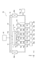
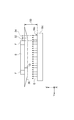
図1は、一実施形態に係る成膜装置を模式的に示す図である。図2は、図1のZ方向から見た成膜装置の一部を模式的に示す図である。図1及び図2には、XYZ直交座標系が示されている。 FIG. 1 is a diagram schematically illustrating a film forming apparatus according to an embodiment. FIG. 2 is a diagram schematically showing a part of the film forming apparatus viewed from the Z direction in FIG. 1 and 2 show an XYZ orthogonal coordinate system.
図1に示される成膜装置10は、基板Sを収容する処理チャンバ12と、基板Sを保持するステージ14とを備える。基板Sは、例えばガラス基板等の透明基板である。基板Sの形状は、例えば矩形である。基板Sの一方の面(成膜面)は例えば鉛直方向において下を向いている。すなわち、成膜装置10はフェースダウン型の成膜装置である。処理チャンバ12には、配管12gを介して真空ポンプ15が接続されている。真空ポンプ15により、処理チャンバ12内を減圧することができる。ステージ14は、基板Sを保持する静電チャックを内蔵してもよい。
A
成膜装置10は、蒸着材料を含むガスGを基板Sに噴き付ける複数のノズル16cを有する蒸着ヘッド18cを備える。成膜装置10は、ノズル16cと同様の構造を有するノズル16a,16b,16d,16e,16fをそれぞれ有する蒸着ヘッド18a,18b,18d,18e,18fを備えてもよい。ノズル16a,16b,16d,16e,16fからは、ノズル16cから噴き出す蒸着材料とは別の蒸着材料であって、かつ、互いに異なる蒸着材料が噴き出してもよい。これにより、基板S上に複数種類の膜を連続的に蒸着させることができる。
The
蒸着ヘッド18a〜18fには、処理チャンバ12外に配置されたガス供給源20a〜20fがそれぞれ配管12a〜12fを介して接続されている。例えば、ガス供給源20cからガスGがノズル16cに供給される。ノズル16a〜16fは、図2に示されるようにそれぞれY方向(第1の方向)に沿って配列される。すなわち、成膜装置10は、いわゆるリニアソース型の成膜装置である。ノズル16a〜16fの先端には例えば円形の開口が形成されている。この開口から蒸着材料を含むガスが放出される。ノズル16a〜16fの開口上には、蒸着材料を遮断可能なシャッター17a〜17fがそれぞれ配置されてもよい。図1ではシャッター17cが開いているので、ノズル16cの開口から噴き出すガスGは基板Sに到達する。シャッター17a,17b,17d,17e,17fは閉じているので、ノズル16a,16b,16d,16e,16fの開口から噴き出すガスは基板Sに到達しない。シャッター17a〜17fは、処理チャンバ12に接続されており、例えばY方向に沿った回転軸を中心に回転する。これにより、シャッター17a〜17fを、必要に応じてノズル16a〜16fの開口上に配置したり当該開口上から退避させたりすることができる。
ガスGに含まれる蒸着材料は、気化した1種類又は複数種類の有機材料であってもよい。ガスGは不活性ガスを含んでもよい。例えば、ガス供給源20a〜20fにおいて、固体の有機材料を加熱して気化させ、不活性ガスにより蒸気材料を搬送する。不活性ガスとしては、例えばAr等の希ガスや窒素等が挙げられる。不活性ガスは、気化した有機材料を搬送するキャリアガスとしての役割を果たす。基板S上には、シャドウマスクを配置してもよい。これにより、基板Sの一方の面において所望の場所に所望の有機材料が選択的に蒸着され、有機膜が形成される。シャドウマスクは、例えば、成膜装置10に基板Sを導入する前にアライナーによって基板Sと位置合わせされる。シャドウマスクの厚みは例えば0.1〜0.2mm程度である。
The vapor deposition material contained in the gas G may be one or more kinds of vaporized organic materials. The gas G may contain an inert gas. For example, in the
成膜装置10は、Y方向と交差するX方向(第2の方向)にステージ14を駆動する駆動装置22を備える。これにより、ノズル16a〜16fに対して相対的に基板SがX方向に沿って移動する。基板Sは、X方向に移動することによって、ノズル16a〜16fの開口に順番に対向配置されることとなる。矢印Aはステージ14の移動方向を示す。ステージ14は、例えば支持部14aによってレール24に接続されている。レール24は処理チャンバ12に接続されている。この場合、駆動装置22によってステージ14及び支持部14aはレール24上をスライドするように移動する。基板Sは、処理チャンバ12に形成されたゲートバルブ26aを通って処理チャンバ12内に導入可能であり、処理チャンバ12に形成されたゲートバルブ26bを通って処理チャンバ12外に搬出可能である。
The
成膜装置10は、図2に示されるように、Y方向に沿った基板Sの側面SaとX方向に沿った基板Sの側面Sbとを覆う枠Fを備える。枠Fは、基板Sの周囲全体を取り囲んでいるが、一部破断していてもよい。枠Fの形状は、例えば板状である。枠Fは、ステージ14と別体である。このため、枠Fが汚れた場合でも交換可能である。枠Fは、例えばガラス、金属等からなる。金属としては、ステンレス、アルミニウム等が挙げられる。枠Fは、基板Sと同じ材料からなってもよい。この場合、枠Fが蒸着処理に与える影響が小さくなる。枠Fの厚みは、例えば0.5〜0.7mmである。基板S上に設けられるシャドウマスクを枠F上にも設けてもよい。これにより、蒸着材料が枠Fに付着して枠Fが汚染されることを抑制できる。
As illustrated in FIG. 2, the
X方向(基板Sの長手方向)における基板Sの長さX2は例えば920mm以上であり、Y方向(短手方向)における基板Sの長さY3は例えば730mm以上である(図2参照)。X方向における枠Fの長さX1は、X方向における基板Sの長さX2より大きい。Y方向における蒸着ヘッド18cの長さY2は、Y方向における基板Sの長さY3より大きい。Y方向における蒸着ヘッド18cの長さY2は、Y方向における枠Fの長さY1以下である。
The length X2 of the substrate S in the X direction (longitudinal direction of the substrate S) is, for example, 920 mm or more, and the length Y3 of the substrate S in the Y direction (short direction) is, for example, 730 mm or more (see FIG. 2). The length X1 of the frame F in the X direction is larger than the length X2 of the substrate S in the X direction. The length Y2 of the
本実施形態の成膜装置10では、Y方向に沿った基板Sの側面Saを枠Fが覆っている。このため、ノズル16cに対して相対的に基板SがX方向に沿って移動した場合に、基板Sの側面Saにおいて、枠Fによって基板Sとステージ14との間の段差が小さくなる。よって、基板Sの側面Saをノズル16cが通過する際に、ノズル16cから噴き出すガスGの流れが変化し難くなる。また、X方向に沿った基板Sの側面Sbにおいても、枠Fによって基板Sとステージ14との間の段差が小さくなるので、ノズル16cから噴き出すガスGの流れが変化し難くなる。したがって、成膜装置10では、基板Sに蒸着される膜の膜厚均一性を向上させることができる。さらに、ガスGが複数種類の蒸着材料を含む場合には、蒸着される膜中の混合比率の深さ分布を均一化することができる。
In the
また、枠Fが基板Sの周囲全体を取り囲む場合、基板Sの周囲全体において、基板Sに蒸着される膜の膜厚均一性を向上させることができる。さらに、枠Fの表面が基板Sの成膜面を延長した仮想面に沿うように設定されていると、基板Sの側面Sa,Sbにおいて、ノズル16cと基板Sとの間の距離とノズル16cと枠Fとの間の距離が略一定になる。その結果、基板Sに蒸着される膜の膜厚均一性を更に向上させることができる。基板Sの成膜面を延長した仮想面に沿うように枠Fの表面を設定するためには、基板Sの厚み方向における枠Fの厚みをS基板の厚みと同じにしてもよい。
Further, when the frame F surrounds the entire periphery of the substrate S, the film thickness uniformity of the film deposited on the substrate S can be improved in the entire periphery of the substrate S. Further, when the surface of the frame F is set so as to be along a virtual plane obtained by extending the film formation surface of the substrate S, the distance between the
また、Y方向における蒸着ヘッド18cの長さY2が、Y方向における基板Sの長さY3よりも大きい場合、基板Sの側面Sbにおいて、基板Sに蒸着される膜の膜厚均一性を更に向上させることができる。さらに、Y方向における蒸着ヘッド18cの長さY2が、Y方向における枠Fの長さY1以下である場合、基板S及び枠Fではなく処理チャンバ12に蒸着材料が付着することを抑制できる。このため、処理チャンバ12内の汚染が抑制され、処理チャンバ12のメンテナンス頻度を少なくすることができる。また、蒸着材料の使用量も抑制することができる。基板Sとノズル16cとの間のギャップ30を狭くすると、枠Fの長さY1を蒸着ヘッド18cの長さY2に近づけても高い膜厚均一性を維持することができる。
Further, when the length Y2 of the
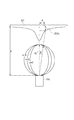
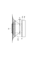
図3は、図1のX方向から見た成膜装置の一部を模式的に示す図である。図3には、XYZ直交座標系が示されている。図3に示されるように、蒸着ヘッド18cのノズル16cから噴き出すガスGが基板S及び枠Fに到達すると、膜36が基板S及び枠F上に形成される。膜36の厚みDは、基板S及び枠F上及び枠Fの外側に位置する片側クリアランス領域32上において略一定である。片側クリアランス領域32から外側では膜36の厚みDは徐々に小さくなる。片側クリアランス領域32の外側には、最も外側のノズル16cの位置まで延びるマージン領域34がある。マージン領域34は、加工精度や取り付け誤差等に起因する成膜装置10の個体差(機差)を吸収可能である。なお、片側クリアランス領域32及びマージン領域34を含む枠Fよりも外側の領域では、膜36は基板S及び枠F上には形成されずに、例えば処理チャンバ12等に付着する。
FIG. 3 is a diagram schematically showing a part of the film forming apparatus viewed from the X direction of FIG. FIG. 3 shows an XYZ orthogonal coordinate system. As shown in FIG. 3, when the gas G ejected from the
図4は、ノズルから噴き出す蒸着材料の空間分布モデルの一例を模式的に示す図である。図4に示されるように、単一のノズル16cから噴き出す蒸着材料の強度Z(X)は以下の式(1)で表される。式(1)中のθは以下の式(2)で表される。
Z(X)=Z0cosnθ … (1)
θ=arctan(X/h) … (2)
Xは、ノズル16cの軸線方向からの距離(変位)を示す。蒸着材料の強度Z(X)は、変位Xにおける蒸着材料の量に対応する。Z0はX=0の場合のZ(X)の値を示す。θは、ノズル16cの軸線方向に対するノズル16cの噴き出し角度を表す。nはノズル16cの開口の寸法に対応するパラメータである。hは、基板S及び枠Fを含む仮想基板S1とノズル16cとの間のギャップ30を表す。
FIG. 4 is a diagram schematically illustrating an example of a spatial distribution model of the vapor deposition material ejected from the nozzle. As shown in FIG. 4, the strength Z (X) of the vapor deposition material ejected from the
Z (X) = Z 0 cos n θ (1)
θ = arctan (X / h) (2)
X shows the distance (displacement) from the axial direction of the
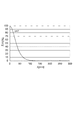
図5は、ノズルから噴き出す蒸着材料の空間分布の一例を示すグラフである。図5に示されるのは、図4に示される空間分布モデルにおいて、n=7の場合の蒸着材料の空間分布である。横軸は変位X(mm)を示す。縦軸は蒸着材料の強度Z(X)(%)を示す。 FIG. 5 is a graph showing an example of the spatial distribution of the vapor deposition material ejected from the nozzle. FIG. 5 shows the spatial distribution of the vapor deposition material when n = 7 in the spatial distribution model shown in FIG. The horizontal axis indicates the displacement X (mm). The vertical axis represents the strength Z (X) (%) of the vapor deposition material.
図6は、ノズルから噴き出す蒸着材料の空間分布の一例を模式的に示す図である。図6では、1次元的に配列された複数のノズル16cに対して図4に示される空間分布モデルを適用した場合の結果が示されている。図6に示される蒸着材料の強度Z(X)は、蒸着される膜の膜厚分布に対応している。仮想基板S1上の蒸着材料の強度Z(X)は所定範囲D内に収まっており、仮想基板S1に蒸着される膜の膜厚均一性が高いことが分かる。図4に示されるモデルにおいて、θを小さくするようにノズル16cの開口の寸法を変化させると、図6に示される蒸着材料の強度Z(X)において両端の傾斜が急になる。その結果、蒸着ヘッド18cの長さを短くできることになり、蒸着材料の使用量が減少する。また、処理チャンバ12内の汚染が抑制され、処理チャンバ12のメンテナンス頻度を少なくすることができる。θを小さくするためには、例えば、ノズル16cの開口の寸法を小さくしてもよい。
FIG. 6 is a diagram schematically illustrating an example of a spatial distribution of the vapor deposition material ejected from the nozzle. FIG. 6 shows a result when the spatial distribution model shown in FIG. 4 is applied to a plurality of
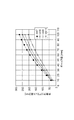
図7は、ノズルと基板との間のギャップ値と片側クリアランス値との関係を示すグラフである。横軸は、図3のギャップ30に対応するギャップ値(mm)を示す。縦軸は、図3の片側クリアランス領域32の幅に対応する片側クリアランス値(mm)を示す。図7のグラフでは、n=7,8,9,11の場合について、ギャップ値に対する片側クリアランス値がプロットされている。片側クリアランス値は、蒸着材料の強度Z(X)が所定の閾値(例えば中心点の強度Z(X)が0.25%以内に保たれる値である)となる場合の値である。図7のグラフによれば、ギャップ値を大きくすると片側クリアランス値も大きくなることが分かる。なお、蒸着材料の強度Z(X)における0.25〜99.75%の部分を用いてプロットを行った(図5参照)。すなわち、X=0付近の99.75〜100%及び0〜0.25%を除去してプロットを行った。
FIG. 7 is a graph showing the relationship between the gap value between the nozzle and the substrate and the one-side clearance value. The horizontal axis indicates a gap value (mm) corresponding to the
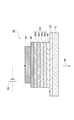
図8は、本実施形態に係る成膜装置を用いて製造される有機EL素子の一例を模式的に示す図である。図8に示される有機EL素子50は、基板S上に形成された陽極52と陰極54とを備えている。陽極52と陰極54との間には、発光層56が設けられている。発光層56と陽極52との間にはホール輸送層58が設けられている。発光層56と陰極54との間には電子輸送層60が設けられている。発光層56は、非発光層56a、青発光層56b、赤発光層56c及び緑発光層56dを備えている。非発光層56a、青発光層56b、赤発光層56c及び緑発光層56dは、ホール輸送層58から電子輸送層60に向かってこの順に設けられている。陽極52と陰極54との間には、配線を介して電源62が接続されている。電源62により電流が発光層56に注入されると、発光層56から放出された光64が陽極52及び基板Sを通過して外部に放出される。
FIG. 8 is a diagram schematically illustrating an example of an organic EL element manufactured using the film forming apparatus according to the present embodiment. The
ホール輸送層58、非発光層56a、青発光層56b、赤発光層56c、緑発光層56d及び電子輸送層60は、成膜装置10により形成可能である。この場合、これら6層を形成するための6種類の蒸着材料をノズル16a〜16fからそれぞれ供給する。成膜装置10を用いると膜厚均一性の高い6層が形成されるので、良好な特性を有する有機EL素子50を製造することができる。
The
以上、本発明の好適な実施形態について詳細に説明したが、本発明は上記実施形態に限定されない。 As mentioned above, although preferred embodiment of this invention was described in detail, this invention is not limited to the said embodiment.
例えば、成膜装置10は、フェースアップ型の成膜装置であってもよい。すなわち、基板Sの一方の面(成膜面)が鉛直方向において上を向いてもよい。また、成膜装置10を用いて、有機EL素子50以外のデバイスを製造することもできる。そのようなデバイスとしては、例えば半導体デバイス、太陽電池、光デバイス、電子デバイス等が挙げられる。さらに、ステージ14に対して蒸着ヘッド18cをX方向に駆動してもよい。
For example, the
10…成膜装置、12…処理チャンバ、14…ステージ、16a〜16f…ノズル、18a〜18f…蒸着ヘッド、22…駆動装置、F…枠、G…蒸着材料を含むガス、S…基板、Sa…第1の方向に沿った基板の側面、Sb…第2の方向に沿った基板の側面。
DESCRIPTION OF
Claims (5)
前記基板を保持するステージと、
蒸着材料を含むガスを前記基板に噴き付ける複数のノズルを有する蒸着ヘッドであり、前記複数のノズルが第1の方向に沿って配列される、前記蒸着ヘッドと、
前記複数のノズルに対して相対的に前記基板が前記第1の方向と交差する第2の方向に沿って移動するように、前記蒸着ヘッド及び前記ステージの少なくとも一方を駆動する駆動装置と、
前記第1の方向に沿った前記基板の側面と前記第2の方向に沿った前記基板の側面とを覆う枠と、
を備える、成膜装置。 A processing chamber containing a substrate;
A stage for holding the substrate;
A deposition head having a plurality of nozzles for spraying a gas containing a deposition material onto the substrate, wherein the plurality of nozzles are arranged along a first direction; and
A driving device that drives at least one of the vapor deposition head and the stage so that the substrate moves along a second direction intersecting the first direction relative to the plurality of nozzles;
A frame that covers a side surface of the substrate along the first direction and a side surface of the substrate along the second direction;
A film forming apparatus comprising:
Priority Applications (1)
| Application Number | Priority Date | Filing Date | Title |
|---|---|---|---|
| JP2011112672A JP2012241237A (en) | 2011-05-19 | 2011-05-19 | Film deposition apparatus |
Applications Claiming Priority (1)
| Application Number | Priority Date | Filing Date | Title |
|---|---|---|---|
| JP2011112672A JP2012241237A (en) | 2011-05-19 | 2011-05-19 | Film deposition apparatus |
Publications (1)
| Publication Number | Publication Date |
|---|---|
| JP2012241237A true JP2012241237A (en) | 2012-12-10 |
Family
ID=47463271
Family Applications (1)
| Application Number | Title | Priority Date | Filing Date |
|---|---|---|---|
| JP2011112672A Withdrawn JP2012241237A (en) | 2011-05-19 | 2011-05-19 | Film deposition apparatus |
Country Status (1)
| Country | Link |
|---|---|
| JP (1) | JP2012241237A (en) |
Cited By (2)
| Publication number | Priority date | Publication date | Assignee | Title |
|---|---|---|---|---|
| KR101477598B1 (en) * | 2014-05-21 | 2014-12-30 | 주식회사 아르케 | Deposition apparatus |
| JP2018003121A (en) * | 2016-07-05 | 2018-01-11 | キヤノントッキ株式会社 | Vapor deposition apparatus and evaporation source |
-
2011
- 2011-05-19 JP JP2011112672A patent/JP2012241237A/en not_active Withdrawn
Cited By (5)
| Publication number | Priority date | Publication date | Assignee | Title |
|---|---|---|---|---|
| KR101477598B1 (en) * | 2014-05-21 | 2014-12-30 | 주식회사 아르케 | Deposition apparatus |
| JP2018003121A (en) * | 2016-07-05 | 2018-01-11 | キヤノントッキ株式会社 | Vapor deposition apparatus and evaporation source |
| CN107574412A (en) * | 2016-07-05 | 2018-01-12 | 佳能特机株式会社 | evaporation device and evaporation source |
| CN107574412B (en) * | 2016-07-05 | 2021-04-27 | 佳能特机株式会社 | Evaporation device and evaporation source |
| CN113151787A (en) * | 2016-07-05 | 2021-07-23 | 佳能特机株式会社 | Evaporation device and evaporation source |
Similar Documents
| Publication | Publication Date | Title |
|---|---|---|
| US10072328B2 (en) | High-precision shadow-mask-deposition system and method therefor | |
| US8802200B2 (en) | Method and apparatus for cleaning organic deposition materials | |
| US8852687B2 (en) | Organic layer deposition apparatus | |
| TWI633197B (en) | High-precision shadow mask deposition system and method thereof | |
| CN106435477B (en) | Organic layer deposition apparatus, organic light emitting display apparatus, and display apparatus manufacturing method | |
| US9174250B2 (en) | Method and apparatus for cleaning organic deposition materials | |
| US11778890B2 (en) | Organic layer deposition apparatus and method of manufacturing organic light-emitting display apparatus using the same | |
| KR102595355B1 (en) | Deposition apparatus and depositon method using the same | |
| KR20100133677A (en) | Thin film deposition apparatus | |
| US8431493B2 (en) | Replaceable substrate masking on carrier and method for processing a substrate | |
| KR20140010304A (en) | Flat panel display device and manufacturing method thereof | |
| JP2013206820A (en) | Organic el device manufacturing apparatus and organic el device manufacturing method | |
| JP2013206820A6 (en) | Organic EL device manufacturing apparatus and organic EL device manufacturing method | |
| JP2012241237A (en) | Film deposition apparatus | |
| WO2020186671A1 (en) | Evaporation deposition equipment and use method thereof | |
| KR20150113742A (en) | Evaporation source and deposition apparatus including the same | |
| TW201418507A (en) | Deposition apparatus and method for manufacturing organic light emitting diode display using the same | |
| KR102132434B1 (en) | Glass deposition apparatus | |
| KR102608846B1 (en) | Deposition sorce and method of manufacturing the same | |
| US9054342B2 (en) | Apparatus and method for etching organic layer | |
| JP2013209696A (en) | Vacuum deposition device and vapor deposition source of the same | |
| KR101648489B1 (en) | Apparatus for depositing thin films and method using the same | |
| US20180309091A1 (en) | Restriction unit, vapor deposition device, production method for vapor deposition film, production method for electroluminescence display device, and electroluminescence display device | |
| KR20150045805A (en) | Thin film deposition apparatus and thin film deposition system | |
| KR102722670B1 (en) | Micro-pattern forming device using electron beam |
Legal Events
| Date | Code | Title | Description |
|---|---|---|---|
| A300 | Withdrawal of application because of no request for examination |
Free format text: JAPANESE INTERMEDIATE CODE: A300 Effective date: 20140805 |