JP2012226041A - Electro-optic device - Google Patents
Electro-optic device Download PDFInfo
- Publication number
- JP2012226041A JP2012226041A JP2011091941A JP2011091941A JP2012226041A JP 2012226041 A JP2012226041 A JP 2012226041A JP 2011091941 A JP2011091941 A JP 2011091941A JP 2011091941 A JP2011091941 A JP 2011091941A JP 2012226041 A JP2012226041 A JP 2012226041A
- Authority
- JP
- Japan
- Prior art keywords
- pixel
- gradation level
- pixels
- frame
- time
- Prior art date
- Legal status (The legal status is an assumption and is not a legal conclusion. Google has not performed a legal analysis and makes no representation as to the accuracy of the status listed.)
- Pending
Links
- 230000008859 change Effects 0.000 claims abstract description 20
- 239000004973 liquid crystal related substance Substances 0.000 claims description 41
- 238000002834 transmittance Methods 0.000 description 15
- 230000004048 modification Effects 0.000 description 14
- 238000012986 modification Methods 0.000 description 14
- 238000006243 chemical reaction Methods 0.000 description 11
- 230000005684 electric field Effects 0.000 description 11
- 238000010586 diagram Methods 0.000 description 10
- 239000003990 capacitor Substances 0.000 description 7
- 238000000034 method Methods 0.000 description 7
- 239000003086 colorant Substances 0.000 description 6
- 230000007423 decrease Effects 0.000 description 6
- 230000005540 biological transmission Effects 0.000 description 3
- 230000000694 effects Effects 0.000 description 2
- 230000006870 function Effects 0.000 description 2
- 238000004519 manufacturing process Methods 0.000 description 2
- 239000011159 matrix material Substances 0.000 description 2
- 230000010287 polarization Effects 0.000 description 2
- 230000003247 decreasing effect Effects 0.000 description 1
- 238000001514 detection method Methods 0.000 description 1
- 229910052736 halogen Inorganic materials 0.000 description 1
- 150000002367 halogens Chemical class 0.000 description 1
- 230000003287 optical effect Effects 0.000 description 1
- 230000008569 process Effects 0.000 description 1
- 230000007480 spreading Effects 0.000 description 1
- 238000003892 spreading Methods 0.000 description 1
- 238000003860 storage Methods 0.000 description 1
- 239000010409 thin film Substances 0.000 description 1
Images


Classifications
-
- G—PHYSICS
- G09—EDUCATION; CRYPTOGRAPHY; DISPLAY; ADVERTISING; SEALS
- G09G—ARRANGEMENTS OR CIRCUITS FOR CONTROL OF INDICATING DEVICES USING STATIC MEANS TO PRESENT VARIABLE INFORMATION
- G09G3/00—Control arrangements or circuits, of interest only in connection with visual indicators other than cathode-ray tubes
- G09G3/20—Control arrangements or circuits, of interest only in connection with visual indicators other than cathode-ray tubes for presentation of an assembly of a number of characters, e.g. a page, by composing the assembly by combination of individual elements arranged in a matrix no fixed position being assigned to or needed to be assigned to the individual characters or partial characters
- G09G3/2007—Display of intermediate tones
- G09G3/2018—Display of intermediate tones by time modulation using two or more time intervals
- G09G3/2022—Display of intermediate tones by time modulation using two or more time intervals using sub-frames
-
- G—PHYSICS
- G09—EDUCATION; CRYPTOGRAPHY; DISPLAY; ADVERTISING; SEALS
- G09G—ARRANGEMENTS OR CIRCUITS FOR CONTROL OF INDICATING DEVICES USING STATIC MEANS TO PRESENT VARIABLE INFORMATION
- G09G3/00—Control arrangements or circuits, of interest only in connection with visual indicators other than cathode-ray tubes
- G09G3/20—Control arrangements or circuits, of interest only in connection with visual indicators other than cathode-ray tubes for presentation of an assembly of a number of characters, e.g. a page, by composing the assembly by combination of individual elements arranged in a matrix no fixed position being assigned to or needed to be assigned to the individual characters or partial characters
- G09G3/34—Control arrangements or circuits, of interest only in connection with visual indicators other than cathode-ray tubes for presentation of an assembly of a number of characters, e.g. a page, by composing the assembly by combination of individual elements arranged in a matrix no fixed position being assigned to or needed to be assigned to the individual characters or partial characters by control of light from an independent source
- G09G3/36—Control arrangements or circuits, of interest only in connection with visual indicators other than cathode-ray tubes for presentation of an assembly of a number of characters, e.g. a page, by composing the assembly by combination of individual elements arranged in a matrix no fixed position being assigned to or needed to be assigned to the individual characters or partial characters by control of light from an independent source using liquid crystals
- G09G3/3611—Control of matrices with row and column drivers
- G09G3/3648—Control of matrices with row and column drivers using an active matrix
-
- G—PHYSICS
- G09—EDUCATION; CRYPTOGRAPHY; DISPLAY; ADVERTISING; SEALS
- G09G—ARRANGEMENTS OR CIRCUITS FOR CONTROL OF INDICATING DEVICES USING STATIC MEANS TO PRESENT VARIABLE INFORMATION
- G09G2300/00—Aspects of the constitution of display devices
- G09G2300/04—Structural and physical details of display devices
- G09G2300/0421—Structural details of the set of electrodes
- G09G2300/0434—Flat panel display in which a field is applied parallel to the display plane
-
- G—PHYSICS
- G09—EDUCATION; CRYPTOGRAPHY; DISPLAY; ADVERTISING; SEALS
- G09G—ARRANGEMENTS OR CIRCUITS FOR CONTROL OF INDICATING DEVICES USING STATIC MEANS TO PRESENT VARIABLE INFORMATION
- G09G2320/00—Control of display operating conditions
- G09G2320/02—Improving the quality of display appearance
- G09G2320/0266—Reduction of sub-frame artefacts
-
- G—PHYSICS
- G09—EDUCATION; CRYPTOGRAPHY; DISPLAY; ADVERTISING; SEALS
- G09G—ARRANGEMENTS OR CIRCUITS FOR CONTROL OF INDICATING DEVICES USING STATIC MEANS TO PRESENT VARIABLE INFORMATION
- G09G3/00—Control arrangements or circuits, of interest only in connection with visual indicators other than cathode-ray tubes
- G09G3/20—Control arrangements or circuits, of interest only in connection with visual indicators other than cathode-ray tubes for presentation of an assembly of a number of characters, e.g. a page, by composing the assembly by combination of individual elements arranged in a matrix no fixed position being assigned to or needed to be assigned to the individual characters or partial characters
- G09G3/34—Control arrangements or circuits, of interest only in connection with visual indicators other than cathode-ray tubes for presentation of an assembly of a number of characters, e.g. a page, by composing the assembly by combination of individual elements arranged in a matrix no fixed position being assigned to or needed to be assigned to the individual characters or partial characters by control of light from an independent source
- G09G3/36—Control arrangements or circuits, of interest only in connection with visual indicators other than cathode-ray tubes for presentation of an assembly of a number of characters, e.g. a page, by composing the assembly by combination of individual elements arranged in a matrix no fixed position being assigned to or needed to be assigned to the individual characters or partial characters by control of light from an independent source using liquid crystals
- G09G3/3611—Control of matrices with row and column drivers
- G09G3/3648—Control of matrices with row and column drivers using an active matrix
- G09G3/3655—Details of drivers for counter electrodes, e.g. common electrodes for pixel capacitors or supplementary storage capacitors
Landscapes
- Engineering & Computer Science (AREA)
- Physics & Mathematics (AREA)
- Computer Hardware Design (AREA)
- General Physics & Mathematics (AREA)
- Theoretical Computer Science (AREA)
- Chemical & Material Sciences (AREA)
- Crystallography & Structural Chemistry (AREA)
- Liquid Crystal Display Device Control (AREA)
- Control Of Indicators Other Than Cathode Ray Tubes (AREA)
- Liquid Crystal (AREA)
Abstract
Description
本発明は、複数のサブフィールドの各々において、画素をオンまたはオフのいずれかで駆動する技術に関する。 The present invention relates to a technique for driving a pixel either on or off in each of a plurality of subfields.
液晶素子などの表示素子を画素として有する電気光学装置において中間階調を表現するために、サブフィールド駆動を用いた技術が提案されている。サブフィールド駆動を用いた技術とは、フレーム(フィールド)を分割した複数のサブフィールド毎に、画素をオンまたはオフのいずれか一方で駆動するとともに、1フレームにおけるオンとオフに駆動された時間の割合を変化させることによって中間階調を表現する技術である(例えば、特許文献1)。 In order to express intermediate gradation in an electro-optical device having a display element such as a liquid crystal element as a pixel, a technique using subfield driving has been proposed. The technique using subfield driving is a method in which a pixel is driven either on or off for each of a plurality of subfields into which a frame (field) is divided, and the time during which one frame is driven on and off. This is a technique for expressing halftones by changing the ratio (for example, Patent Document 1).
特許文献1に記載された技術のように、サブフィールド駆動においては、各サブフィールドにおける画素の駆動内容(オンまたはオフ)を1フレーム分規定したサブフィールドコード(以下、SFコードという)が用いられる。このSFコードに基づいて、各画素の液晶素子にオン電圧またはオフ電圧が印加される。隣接した画素において指定された階調レベルが異なる場合、それぞれのSFコードのうち駆動内容が異なるサブフィールドの期間においては、隣接画素間においてオン電圧とオフ電圧との差から横電界が発生する。この横電界の影響により隣接画素間にはディスクリネーションが発生し、表示に影響を与える。そのため、隣接した画素において駆動内容が異なるサブフィールドが多いほど、隣接画素間に発生するディスクリネーションの表示への影響が大きくなる。 As in the technique described in Patent Document 1, in subfield driving, a subfield code (hereinafter referred to as SF code) that defines the driving contents (on or off) of pixels in each subfield for one frame is used. . Based on the SF code, an on voltage or an off voltage is applied to the liquid crystal element of each pixel. When the designated gradation levels are different in adjacent pixels, a lateral electric field is generated between adjacent pixels due to the difference between the on-voltage and the off-voltage in the sub-field period of different driving contents in each SF code. Due to the influence of the horizontal electric field, disclination occurs between adjacent pixels, which affects the display. Therefore, the more subfields having different driving contents in adjacent pixels, the greater the influence on the display of disclination that occurs between adjacent pixels.
ここで、少ないサブフィールド数で多くの階調レベルの表現をする場合には、各サブフィールドの時間を大きく異ならせて、サブフィールドの時間に重み付けする必要がある。このような場合には、隣接階調レベル間において長い時間のサブフィールドの駆動内容が異なる場合もある。隣接する画素の階調レベルは隣接する階調レベルとなることがあるが、上記の場合には、横電界が発生する時間も長くなり、隣接画素間に発生するディスクリネーションの表示に与える影響が大きくなる。 Here, when expressing a large number of gradation levels with a small number of subfields, it is necessary to weight the subfield times by making the time of each subfield significantly different. In such a case, the driving content of the subfield for a long time may be different between adjacent gradation levels. The gradation level of adjacent pixels may be the adjacent gradation level, but in the above case, the time during which the horizontal electric field is generated becomes longer, and the influence on the display of the disclination generated between adjacent pixels. Becomes larger.
本発明は、上述した事情に鑑みてなされたものであり、その目的の一つは、隣接階調レベル間において長い時間のサブフィールドの駆動内容が異なる場合であっても、その駆動内容の違いに起因するディスクリネーションの表示に与える影響を抑えることにある。 The present invention has been made in view of the above-described circumstances, and one of the purposes thereof is a difference in driving contents even when the driving contents of a subfield for a long time are different between adjacent gradation levels. It is to suppress the influence on the display of the disclination caused by.
上述の課題を解決するため、本発明は、各々が液晶素子を有する複数の画素と、前記画素に対して指定される階調レベルに応じて、1フレームを分割したサブフィールド毎に当該画素を明状態または暗状態に駆動する駆動部とを具備し、1フレームにおける少なくとも一の前記サブフィールドの時間は他の前記サブフィールドの時間とは異なり、前記駆動部は、前記複数の画素に特定の階調レベルが指定された場合に、少なくとも一の前記画素と、当該一の画素に隣接する前記画素とは1フレーム中の駆動内容が異なるように、前記画素を駆動し、前記特定の階調レベルは、隣接する暗い側の階調レベルから当該特定の階調レベルに変化した場合において、前記一の画素の前記駆動内容が、暗状態から明状態に変化したサブフィールドのうち最も長い時間のサブフィールドと、変化後の当該駆動内容が明状態であるサブフィールドのうち最も長い時間のサブフィールドとが一致する関係を満たし、前記隣接する画素の前記駆動内容が、当該関係を満たさない階調レベルを示すことを特徴とする電気光学装置を提供する。
この電気光学装置によれば、隣接階調レベル間において長い時間のサブフィールドの駆動内容が異なる場合であっても、その駆動内容の違いに起因するディスクリネーションの表示に与える影響を抑えることができる。
In order to solve the above-described problem, the present invention relates to a plurality of pixels each having a liquid crystal element and a pixel for each subfield divided into one frame according to a gradation level designated for the pixel. A driving unit that drives in a bright state or a dark state, and the time of at least one of the subfields in one frame is different from the time of the other subfield, and the driving unit is specific to the pixels. When a gradation level is specified, the pixel is driven so that at least one of the pixels and the pixel adjacent to the one pixel have different driving contents in one frame, and the specific gradation The level is a subfield in which the driving content of the one pixel changes from a dark state to a bright state when the adjacent dark side gradation level changes to the specific gradation level. Satisfy the relationship in which the subfield of the long time matches the subfield of the longest time among the subfields in which the drive content after the change is in the bright state, and the drive content of the adjacent pixel satisfies the relationship An electro-optical device is provided that exhibits a gray level that is not satisfied.
According to this electro-optical device, even when the driving content of the subfield for a long time differs between adjacent gradation levels, the influence on the display of the disclination due to the difference in the driving content can be suppressed. it can.
また、本発明は、各々が液晶素子を有する複数の画素と、前記画素に対して指定される階調レベルに応じて、1フレームを分割したサブフィールド毎に当該画素を明状態または暗状態に駆動する駆動部とを具備し、1フレームにおける少なくとも一の前記サブフィールドの時間は他の前記サブフィールドの時間とは異なり、前記駆動部は、前記複数の画素に特定の階調レベルが指定された場合に、少なくとも一の前記画素と、当該一の画素に隣接する前記画素とは1フレーム中の駆動内容が異なるように、前記画素を駆動し、前記特定の階調レベルは、隣接する暗い側の階調レベルから当該特定の階調レベルに変化した場合において、前記一の画素の前記駆動内容が、変化後の当該駆動内容が明状態であるサブフィールドの時間の合計に対する前記駆動内容が変化したサブフィールドの時間の合計の割合が予め決められた割合以上になる関係を満たし、前記隣接する画素の前記駆動内容が、当該関係を満たさない階調レベルを示すことを特徴とする電気光学装置を提供する。
この電気光学装置によれば、隣接階調レベル間において長い時間のサブフィールドの駆動内容が異なる場合であっても、その駆動内容の違いに起因するディスクリネーションの表示に与える影響を抑えることができる。
In addition, according to the present invention, a plurality of pixels each having a liquid crystal element and a pixel in a bright state or a dark state for each subfield divided into one frame according to a gradation level designated for the pixel. A drive unit for driving, wherein a time of at least one of the subfields in one frame is different from a time of the other subfield, and the drive unit assigns a specific gradation level to the plurality of pixels. The at least one pixel and the pixel adjacent to the one pixel are driven such that the driving content in one frame is different, and the specific gradation level is adjacent to dark When the gradation level on the side changes to the specific gradation level, the drive content of the one pixel is relative to the total time of subfields in which the drive content after the change is in a bright state. The ratio of the total time of the subfields in which the drive content has changed satisfies a relationship that is equal to or greater than a predetermined rate, and the drive content of the adjacent pixels indicates a gray level that does not satisfy the relationship. An electro-optical device is provided.
According to this electro-optical device, even when the driving content of the subfield for a long time differs between adjacent gradation levels, the influence on the display of the disclination due to the difference in the driving content can be suppressed. it can.
また、別の好ましい態様において、前記液晶素子は、ノーマリーブラックモードで駆動され、前記特定の階調レベルにおける1フレーム中の明状態の時間は、当該階調レベルに隣接する暗い側と明るい側との階調レベルにおける1フレーム中の明状態の時間の平均よりも長くなるように決められていることを特徴とする。
この電気光学装置によれば、ノーマリーブラックモードにおいて、連続した画素に同一の階調レベルが指定された場合に、連続した画素間においてディスクリネーションが生じて透過率が減少しても、これらの画素全体として指定された階調レベルの表現をすることができる。
In another preferred embodiment, the liquid crystal element is driven in a normally black mode, and the time of the bright state in one frame at the specific gradation level is the dark side and the bright side adjacent to the gradation level. It is determined to be longer than the average of the time of the bright state in one frame at the gradation level.
According to this electro-optical device, in the normally black mode, when the same gradation level is designated for consecutive pixels, even if disclination occurs between consecutive pixels and the transmittance decreases, these The gradation level specified for the entire pixel can be expressed.
また、別の好ましい態様において、前記液晶素子は、ノーマリーホワイトモードで駆動され、前記特定の階調レベルにおける1フレーム中の明状態の時間は、当該階調レベルに隣接する暗い側と明るい側との階調レベルにおける1フレーム中の明状態の時間の平均よりも短くなるように決められていることを特徴とする。
この電気光学装置によれば、ノーマリーホワイトモードにおいて、連続した画素に同一の階調レベルが指定された場合に、連続した画素間においてディスクリネーションが生じて透過率が減少しても、これらの画素全体として指定された階調レベルの表現をすることができる。
In another preferable aspect, the liquid crystal element is driven in a normally white mode, and the time of the bright state in one frame at the specific gradation level is the dark side and the bright side adjacent to the gradation level. The gray level is determined so as to be shorter than the average of the time of the bright state in one frame.
According to this electro-optical device, in the normally white mode, when the same gradation level is designated for consecutive pixels, even if disclination occurs between consecutive pixels and the transmittance decreases, these The gradation level specified for the entire pixel can be expressed.
また、別の好ましい態様において、前記液晶素子は、ノーマリーブラックモードで駆動され、前記特定の階調レベルにおける1フレーム中の明状態の時間は、当該階調レベルに隣接する明るい側の階調レベルにおける1フレーム中の明状態の時間よりも長くなるように決められていることを特徴とする。
この電気光学装置によれば、ノーマリーブラックモードにおいて、連続した画素に同一の階調レベルが指定された場合に、連続した画素間においてディスクリネーションが生じて透過率が減少しても、これらの画素全体として指定された階調レベルの表現をすることができる。
In another preferable aspect, the liquid crystal element is driven in a normally black mode, and the time of the bright state in one frame at the specific gradation level is the gradation on the bright side adjacent to the gradation level. The level is determined to be longer than the time of the bright state in one frame in the level.
According to this electro-optical device, in the normally black mode, when the same gradation level is designated for consecutive pixels, even if disclination occurs between consecutive pixels and the transmittance decreases, these The gradation level specified for the entire pixel can be expressed.
また、別の好ましい態様において、前記液晶素子は、ノーマリーホワイトモードで駆動され、前記特定の階調レベルにおける1フレーム中の明状態の時間は、当該階調レベルに隣接する暗い側の階調レベルにおける1フレーム中の明状態の時間よりも短くなるように決められていることを特徴とする。
この電気光学装置によれば、ノーマリーホワイトモードにおいて、連続した画素に同一の階調レベルが指定された場合に、連続した画素間においてディスクリネーションが生じて透過率が減少しても、これらの画素全体として指定された階調レベルの表現をすることができる。
In another preferred embodiment, the liquid crystal element is driven in a normally white mode, and the time of the bright state in one frame at the specific gradation level is a dark side gradation adjacent to the gradation level. It is characterized in that it is determined to be shorter than the time of the bright state in one frame in the level.
According to this electro-optical device, in the normally white mode, when the same gradation level is designated for consecutive pixels, even if disclination occurs between consecutive pixels and the transmittance decreases, these The gradation level specified for the entire pixel can be expressed.
また、別の好ましい態様において、前記駆動部は、前記複数の画素における前記少なくとも一の画素の位置を、1フレームまたは複数フレーム毎に変化させるように、前記画素を駆動することを特徴とする。
この電気光学装置によれば、隣接階調レベル間において長い時間のサブフィールドの駆動内容が異なる場合であっても、その駆動内容の違いに起因するディスクリネーションの表示に与える影響を、効果的に抑えることができる。
In another preferable aspect, the driving unit drives the pixel so that the position of the at least one pixel in the plurality of pixels is changed for each frame or every plurality of frames.
According to this electro-optical device, even when the driving contents of the subfield for a long time are different between adjacent gradation levels, the effect on the display of the disclination due to the difference in the driving contents is effectively reduced. Can be suppressed.
また、別の好ましい態様において、前記駆動部は、前記複数の画素に前記特定の階調レベルが指定された場合に、全ての前記画素を、隣接する前記画素とは1フレーム中の前記駆動内容が異なるように駆動することを特徴とする。
この電気光学装置によれば、隣接階調レベル間において長い時間のサブフィールドの駆動内容が異なる場合であっても、その駆動内容の違いに起因するディスクリネーションの表示に与える影響を、効果的に抑えることができる。
In another preferable aspect, when the specific gradation level is designated for the plurality of pixels, the driving unit sets all the pixels to the adjacent pixels and the driving content in one frame. Are driven differently.
According to this electro-optical device, even when the driving contents of the subfield for a long time are different between adjacent gradation levels, the effect on the display of the disclination due to the difference in the driving contents is effectively reduced. Can be suppressed.
また、別の好ましい態様において、前記駆動部は、前記複数の画素に前記特定の階調レベルが指定された場合に、前記少なくとも一の画素における明状態の時間と、前記隣接する画素における明状態の時間との差は、これらの和に対して10%以内となるように、前記画素を駆動することを特徴とする。
この電気光学装置によれば、階調レベルを良好に表現した表示を行うことができる。
In another preferable aspect, when the specific gradation level is designated for the plurality of pixels, the driving unit performs a bright state time in the at least one pixel and a bright state in the adjacent pixels. The pixel is driven so that the difference from the time is within 10% of the sum thereof.
According to this electro-optical device, it is possible to perform display in which gradation levels are well expressed.
<実施形態>
[プロジェクター2000の構成]
図1は、実施形態におけるプロジェクター2000の構成を示す平面図である。プロジェクター2000は、ハロゲンランプ等の白色光源となるランプユニット220を有する。ランプユニット220から射出された投射光は、第1マルチレンズ2303、第2マルチレンズ2304、偏光変換素子2305、重畳レンズ2306を通過し、2枚のダイクロイックミラー2301および3枚のミラー2302によってR(赤)、G(緑)、B(青)の3原色に分離される。分離された各光は、集光レンズ2308を介して、各原色に対応する表示パネル100R、100Gおよび100Bにそれぞれ導かれる。なお、B光は、R光、G光と比較すると、光路が長いことによる損失を防ぐために、3枚のレンズ2307を用いたリレーレンズ系を介して導かれる。
<Embodiment>
[Configuration of Projector 2000]
FIG. 1 is a plan view illustrating a configuration of a
表示パネル100R、100G、100Bは、光を変調する液晶パネルなどのライトバルブである。表示パネル100R、100G、100Bは、後述するように、R、G、Bの各色に対応する映像信号Vidを画素毎に決められたLUT(Look up Table)を参照して変換したSFコードに基づいてそれぞれ駆動される。これにより、表示パネル100R、100G、100Bには、各色の縮小画像が形成される。表示パネル100R、100G、100Bによってそれぞれ形成された縮小画像、すなわち、変調光は、ダイクロイックプリズム240に3方向から入射する。そして、このダイクロイックプリズム240において、R光およびB光は90度に反射する一方、G光は直進する。したがって、各色の画像が合成された後、スクリーン3000には、投射レンズ250によってカラー画像が投射されることとなる。
The
なお、表示パネル100R、100G、100Bには、ダイクロイックミラー2301によって、R色、G色、B色のそれぞれに対応する光が入射するので、カラーフィルタを設ける必要はない。また、表示パネル100R、100Bの透過像は、ダイクロイックプリズム240により反射した後に投射されるのに対し、表示パネル100Gの透過像はそのまま投射されるので、表示パネル100R、100Bによる水平走査方向は、表示パネル100Gによる水平走査方向と逆向きにして、左右を反転させた像を表示する構成となっている。
Since light corresponding to each of the R color, G color, and B color is incident on the
[機能構成]
図2は、実施形態におけるプロジェクター2000の機能構成を説明する図である。プロジェクター2000は、表示パネル100R、100G、100Bに縮小画像を形成させるための駆動部であるコントローラー10と、表示パネル100R、100G、100Bと、複数のLUTを有する。コントローラー10は、タイミング制御回路11、画質調整部12、SFコード変換部13、メモリー制御部14、メモリー15、駆動回路16R、16G、16Bを有する。複数のLUTは、この例においては、LUT(A)31およびLUT(B)32である。
なお、表示パネル100R、100G、100Bは、各々同じ構成であるため、以下の説明において特にそれぞれを区別する必要のない場合には、表示パネル100と記す。
[Function configuration]
FIG. 2 is a diagram illustrating a functional configuration of the
Since the
コントローラー10には、図示省略した上位回路から映像信号Vidおよび同期信号Syncが供給される。映像信号Vidは、画像を3つの原色(赤(R)色、緑(G)色、青(B)色の三成分)で表す信号である。映像信号Vidは、画像における各画素の階調レベルをR、G、Bの色毎にそれぞれ規定する。なお、映像信号Vidは、同期信号Syncに含まれる垂直走査信号、水平走査信号などにしたがって走査される画素の順で供給される。
The
タイミング制御回路11は、同期信号Syncに基づいて各部を制御する。
画質調整部12は、映像信号Vidで規定される画像の明るさおよび色合いなどを、表示パネル100の表示特性、図示省略した各種操作子を用いて設定された内容に合わせて前処理するとともに、処理した映像信号Daを出力する。なお、この例において、上位回路から供給される映像信号Vidは、アナログ信号でもあってもよいし、デジタル信号でもあってもよいが、アナログ信号であれば、画質調整部12によってデジタル信号に変換される。
なお、この例においては、映像信号Daを8ビットとして、各画素において表現すべき階調レベルを十進値で、最も暗い「0」から最も明るい「255」まで「1」刻みで256段階の階調レベルを指定している。
The
The image
In this example, the video signal Da is 8 bits, and the gradation level to be expressed in each pixel is a decimal value in 256 steps in increments of “1” from the darkest “0” to the brightest “255”. The gradation level is specified.
SFコード変換部13は、LUT(A)31およびLUT(B)32を参照して、映像信号Daの階調レベルを、R成分、G成分、B成分の色毎にSFコードScr、Scg、Scbに変換して出力するものである。SFコード変換部13は、LUT(A)31およびLUT(B)32のうち、各画素に対応して予め決められたいずれか一方を参照する。このSFコードScr、Scg、Scbは、ビットc1、c2、・・・c16の16ビットのブロックを2回繰り返した32ビットで構成される。各ビットは各サブフィールドにおける画素の駆動内容を示し、オンに駆動するサブフィールドを「1」、オフに駆動するサブフィールドを「0」として示している。すなわち、SFコードは、1フレームを32のサブフィールドに分割した各サブフィールドにおける画素の駆動内容を示している。なお、この例においては、後述するように、液晶素子120は、ノーマリーブラックモードでの駆動されるものとする。したがって、オンに駆動するサブフィールドは明状態となり、オフに駆動するサブフィールドは暗状態となる。
The SF
メモリー制御部14は、タイミング制御回路11による制御にしたがって、SFコードScr、Scg、Scbをメモリー15に書きこむ。また、メモリー制御部14は、タイミング制御回路11による制御にしたがって、メモリー15に記憶されたSFコードScr、Scg、Scbを読み出し、読み出したSFコードのビットのうち、表示パネル100における駆動タイミング(サブフィールド)に対応するビットをSFビットSbr、Sbg、Sbbとして出力する。例えば、表示パネル100における駆動タイミングが13番目のサブフィールドとなるSFビットは、ビットc13となる。
The
[表示パネル100Rおよび駆動回路16Rの構成]
図3は、実施形態における表示パネル100Rおよび駆動回路16Rの構成を説明する図である。表示パネル100Rは、例えばアクティブ・マトリクス型であって透過型の液晶表示パネルであり、画素毎に透過率を変調した透過像を生成するものである。
図3に示されるように、表示パネル100Rには、例えば1、2、3、…、1080行の走査線112が図において横方向に延在するように設けられ、また、1、2、3、…、1920列のデータ線114が図において縦方向に延在するように、かつ、各走査線112と互いに電気的に絶縁を保つように設けられている。そして、1080行の走査線112と1920列のデータ線114との交点のそれぞれに対応して、画素110がそれぞれ配列している。したがって、画素110が縦1080行×横1920列でマトリクス状に配列することになる。
[Configuration of
FIG. 3 is a diagram illustrating the configuration of the
As shown in FIG. 3, for example, 1, 2, 3,..., 1080 rows of scanning
表示パネル100Rの周辺には、駆動回路16Rが設けられている。駆動回路16Rは、走査線駆動回路161とデータ線駆動回路162とを有する。走査線駆動回路161は、1〜1080行の走査線112にそれぞれ走査信号を供給する。この例においては、走査線駆動回路161は、タイミング制御回路11から供給される制御信号Yctによって走査線112を1、2、3、…、1080行目という順番で選択するとともに、選択した走査線への走査信号を選択電圧とする一方、それ以外の、非選択に係る走査線への走査信号を非選択電圧とする。なお、図3において、1、2、3、…、1080行目の走査線112に供給される走査信号をそれぞれG1、G2、G3、・・・G1080と表記している。
A
データ線駆動回路162は、タイミング制御回路11から供給される制御信号Xctにしたがって、1〜1920列目のデータ線114の各々にそれぞれデータ信号を供給する。データ線駆動回路162は、メモリー制御部14から供給されるSFビットSbrに応じたデータ信号を供給する。なお、図3において、1、2、3、…、1920列目のデータ線114に供給されるデータ信号を、それぞれd1、d2、d3、・・・d1920と表記している。
The data line driving
ここでは、表示パネル100Rおよび駆動回路16Rを例として説明し、同様な構成である表示パネル100G、100Bおよび駆動回路16G、16Bについては、供給される信号が異なるだけであるため、その説明を省略する。なお、表示パネル100Gのデータ線駆動回路162は、メモリー制御部14からSFビットSbgが供給され、SFビットSbrに応じたデータ信号を供給する。また、表示パネル100Bのデータ線駆動回路162は、メモリー制御部14からSFビットSbbが供給され、SFビットSbbに応じたデータ信号を供給する。
Here, the
[画素110の構成]
図4は、実施形態における画素110の等価回路を説明する図である。画素110は、画素電極118とコモン電極108とで液晶105を挟持した液晶素子120と、走査線112に選択電圧が印加されたときにデータ線114と画素電極118との間で導通状態となり、非選択電圧が印加されたときに非導通状態となる薄膜トランジスター(Thin Film Transistor:以下単に「TFT」と表記する)116とを有する構成である。
コモン電極108は各画素にわたって共通であり、コントローラー10に含まれる図示省略した回路によって電圧LCcomが印加される。また、画素110では、液晶素子120に対して並列に補助容量(蓄積容量)125が設けられる。この補助容量125は、一端が画素電極118に接続され、他端が容量線115に共通接続されている。コントローラー10に含まれる図示省略した回路によって、容量線115は時間的に一定の電圧に保たれている。
[Configuration of Pixel 110]
FIG. 4 is a diagram illustrating an equivalent circuit of the
The
このような構成において、画素110では、走査線112に選択電圧が印加されたときにTFT116が導通状態になって、データ線114に供給されたデータ信号の電圧が画素電極118に印加される。一方、走査線112への選択電圧の印加が終了して非選択電圧が印加されたときにTFT116が非導通状態になるが、液晶素子120は、TFT116の導通状態であったときに画素電極118に印加されたデータ信号の電圧を、その容量性によって走査線112に選択電圧が再び印加されるまで保持する。
In such a configuration, in the
ところで、画素110はオンまたはオフのいずれかで駆動されるため、データ信号は、SFビットの「1」に応じたオンレベル、または「0」に応じたオフレベルのいずれかとなる。この例においては、液晶素子120がノーマリーブラックモードで駆動される。そのため、オンレベルとは、液晶素子120に電圧(例えば5V)を印加して明状態にさせるデータ信号をいい、オフレベルとは、液晶素子120に電圧を印加しないで(または、印加電圧をゼロ近傍とする電圧を印加して)暗状態にさせるデータ信号をいう。
この例においては、液晶素子120を交流駆動するため、オンレベルは、振幅中心電圧に対して高位側とする正極性と、振幅中心電圧に対して低位側とする負極性との2種類が必要となる。なお、交流駆動しない場合には、一方の極性のみでよい。
一方、オフレベルは、液晶素子120に電圧を印加しないのであれば、コモン電極108に印加される電圧LCcomの1種類であり、極性に無関係である。液晶素子120を交流駆動し、印加電圧をゼロ近傍とする電圧を印加するのであれば、振幅中心電圧に対して正極性と、負極性との2種類が必要となる。なお、交流駆動しない場合には、一方の極性のみでよい。
Incidentally, since the
In this example, since the
On the other hand, the off level is one type of voltage LCcom applied to the
なお、本説明において、走査信号やデータ信号の電圧については、図示省略した接地電位GNDを電圧ゼロの基準としている。ただし、液晶素子120の印加電圧については、コモン電極108の電圧LCcomと画素電極118との電位差とする。また、コモン電極108に印加される電圧LCcomは、上記振幅中心電圧と同電圧と考えてよい。ただし、nチャネル型のTFT116のオフリーク等を考慮して、電圧LCcomを振幅中心電圧よりも低位となるように調整されることがある。
In this description, for the voltages of the scanning signal and the data signal, the ground potential GND (not shown) is used as a reference of zero voltage. However, the voltage applied to the
[画素110の駆動態様]
図5は、実施形態における駆動回路16R、16G、16Bに供給される信号を説明する図である。ここでは、供給される信号のうち、制御信号Yctに含まれる垂直同期信号Vsync、およびスタートパルスDy、制御信号Xctに含まれる極性指定信号Frpについて説明する。
図5(a)に示すように、垂直同期信号Vsyncは、表示の単位期間である1フレームを規定する信号である。この例においては、1フレームは16.67ms(60Hz)に相当する。極性指定信号Frpは、液晶素子120を交流駆動するときのオンレベルを正極性とする期間と負極性とする期間を規定する信号である。この極性指定信号Frpによっては、1フレームの前半を正極性の期間、後半を負極性の期間として規定する。これにより液晶素子120に印加される電圧の極性バランスをとることができる。
[Driving Mode of Pixel 110]
FIG. 5 is a diagram illustrating signals supplied to the
As shown in FIG. 5A, the vertical synchronization signal Vsync is a signal that defines one frame that is a unit period of display. In this example, one frame corresponds to 16.67 ms (60 Hz). The polarity designation signal Frp is a signal that defines a period in which the on level when the
スタートパルスDyは、各サブフィールドの期間を規定する信号である。スタートパルスDyは、この例においては、8パルスを1周期として1フレームにつき4回繰り返し、1フレームでは32パルスとなる。したがって、1フレームは32のサブフィールドに分割されている。以下、この1周期の8サブフィールド(図5(a)における「8SF」)を1ブロックといい、1フレーム中の各ブロックを期間の最初から第1ブロック、第2ブロック、第3ブロック、第4ブロック(図5(a)における「第1B」、「第2B」、「第3B」、「第4B」)という。
スタートパルスDyにおける1周期の8パルスは、それぞれのパルス間隔が異なり、各間隔がサブフィールドの期間を示し、以下、各サブフィールドをSF1,SF2、・・・、SF8という。この例においては、SF1、SF2、・・・、SF8の時間は、図5(b)に示すように、1.40ms、0.90ms、0.70ms、0.50ms,0.32ms、0.20ms、0.10ms、0.05msと規定され、時間に重み付けがされている。この例においては、1周期のうち前の期間に位置するサブフィールドほど長い時間として規定されている。
なお、各画素におけるサブフィールドのオン駆動(オンレベルの駆動電圧を印加)またはオフ駆動(オフレベルの駆動電圧を印加)は、走査線の選択時になされる。そのため、厳密にいえば、各画素における1フレーム(および各サブフィールド)のタイミングは、時間的にみて走査線毎に異なる。
The start pulse Dy is a signal that defines the period of each subfield. In this example, the start pulse Dy is repeated four times per frame with 8 pulses as one cycle, and becomes 32 pulses in one frame. Therefore, one frame is divided into 32 subfields. Hereinafter, the 8 subfields in one cycle (“8SF” in FIG. 5A) are referred to as one block, and each block in one frame is defined as the first block, the second block, the third block, the first block from the beginning of the period. This is referred to as 4 blocks ("1B", "2B", "3B", "4B" in FIG. 5A).
The eight pulses of one cycle in the start pulse Dy have different pulse intervals, and each interval indicates a subfield period. Hereinafter, each subfield is referred to as SF1, SF2,..., SF8. In this example, the times of SF1, SF2,..., SF8 are 1.40 ms, 0.90 ms, 0.70 ms, 0.50 ms, 0.32 ms,. It is specified as 20 ms, 0.10 ms, and 0.05 ms, and time is weighted. In this example, a subfield located in the previous period of one cycle is defined as a longer time.
Note that on-drive (applying an on-level drive voltage) or off-drive (applying an off-level drive voltage) of a subfield in each pixel is performed when a scanning line is selected. Therefore, strictly speaking, the timing of one frame (and each subfield) in each pixel differs for each scanning line in terms of time.
上述したように、画素110において、走査線112が選択されたときに画素電極118に印加されたオンレベルまたはオフレベルは、走査線112が再び選択されるまで保持される。したがって、画素110を、あるサブフィールドに応じた期間だけオンまたはオフ駆動の状態にさせるためには、走査線を選択して、液晶素子120にSFビットに応じた(データ信号の)オンレベルまたはオフレベルを書き込んでから、再び当該走査線を選択するまでの期間を、当該サブフィールドに応じた期間とすればよいことになる。
As described above, in the
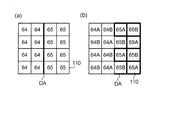
図6は、実施形態における各画素110に適用されるLUTを説明する図である。上述したように、SFコード変換部13は、画素毎にLUT(A)31およびLUT(B)32のいずれか一方を参照して、映像信号DaをSFコードに変換する。図6は、このときに参照するLUTを示すものであり、「A」は、LUT(A)31を参照して得られたSFコードに基づいて駆動される画素110(以下、画素110Aという)を示し、「B」は、LUT(B)32を参照して得られたSFコードに基づいて駆動される画素110(以下、画素110Bという)を示している。
FIG. 6 is a diagram illustrating the LUT applied to each
この例においては、画素110Aは、奇数行の走査線と奇数列のデータ線との交点に対応して設けられた画素110、および偶数行の走査線と偶数列のデータ線との交点に対応して設けられた画素110である。一方、画素110Bは、画素110A以外の画素110である。すなわち、画素110Bは、奇数行の走査線と偶数列のデータ線との交点に対応して設けられた画素110、および偶数行の走査線と奇数列のデータ線との交点に対応して設けられた画素110である。このように、画素110Aに隣接する画素110は、画素110Bになるように配置されている。すなわち、画素110Aと画素110Bとは市松状に配置される。
In this example, the pixel 110A corresponds to the
[LUTの内容]
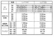
図7は、実施形態におけるLUTを説明する図である。図7(a)はLUT(A)31を示し、図7(b)はLUT(B)32を示している。いずれも、階調レベルが「50」〜「80」の部分を抜き出したものを記載している。LUT(A)31およびLUT(B)32は、ビットc1、c2、・・・、c16の16ビットにより構成され、前半のビットc1からc8の8ビットは、1フレーム中の第1、第3ブロックにおけるSF1、SF2、・・・SF8の画素110の駆動内容を表し、後半のビットc9からc16は、第2、第4ブロックにおけるSF1、SF2、・・・SF8の画素110の駆動内容を表す。そのため、例えば、ビットc1とc9とは、対応するサブフィールドの時間が同じである。その他の関係、例えば、ビットc8とc16との関係などについても、対応するサブフィールドの時間が同じになるという関係は同様である。このように、LUTは、階調レベルと各ビットにより表されるSFコードとの対応関係を規定する。
[Contents of LUT]
FIG. 7 is a diagram illustrating the LUT according to the embodiment. FIG. 7A shows the LUT (A) 31, and FIG. 7B shows the LUT (B) 32. In both cases, the gradation levels “50” to “80” are extracted. LUT (A) 31 and LUT (B) 32 are composed of 16 bits of bits c1, c2,..., C16, and the 8 bits of the first half bits c1 to c8 are the first and third bits in one frame. The driving contents of the
LUTは、後述する一部の例外を除き原則として、階調レベルが上がるほど、1フレーム中に画素110がオンとして駆動される明状態の時間(以下、オン時間という)が長くなるように、各ビットを規定している。一部の階調レベルについては、隣接する低い側の階調レベルから変化した場合のSFコードの変化において、「0」から「1」に変化したビットのうち最も長い時間のサブフィールドが、変化後のSFコードの「1」のビットのうち最も長い時間のサブフィールドと一致する関係を満たしている。例えば、図7(a)に示す範囲のLUT(A)31においては、一部の階調レベルは、「56」、「65」、「78」である。以下、このような関係を満たす階調レベルを最大重み変化部という。
The LUT is, as a general rule, with the exception of some exceptions to be described later, as the gradation level increases, the bright state time (hereinafter referred to as the “on time”) during which the
ここで、階調レベルが「56」の場合には、「55」からのSFコードの変化において、ビットc8、c11が「0」から「1」に変化しているが、最も長い時間のサブフィールドは、ビットc11に対応するSF3である。一方、変化後のSFコードの「1」のビットのうち最も長い時間のサブフィールドもSF3(ビットc3、c11)であり一致している。 Here, when the gradation level is “56”, the bits c8 and c11 are changed from “0” to “1” in the change of the SF code from “55”. The field is SF3 corresponding to the bit c11. On the other hand, the subfield of the longest time among the bits of “1” of the SF code after the change is also SF3 (bits c3 and c11), which match.
LUT(B)32においては、最大重み変化部は、LUT(A)31における場合と異なる階調レベルになるように決められ、この例においては階調レベルが「1」大きくなるように決められている。すなわち、LUT(B)32における最大重み変化部は、「57」、「66」、「79」である。したがって、LUT(A)31またはLUT(B)32の最大重み変化部に対応する階調レベルについて、LUT(A)31とLUT(B)32とは、SFコードが異なっている。なお、この例においては、それ以外の階調レベルにおいても、LUT(A)31とLUT(B)32とにおいてSFコードが異なるものがあるが、これは、ディザリングを用いて階調制度を向上させるためのものである。そのため、最大重み変化部に対応する階調レベル以外は、LUT(A)31とLUT(B)32とでSFコードが同じであってもよい。 In the LUT (B) 32, the maximum weight changing unit is determined to have a gradation level different from that in the LUT (A) 31, and in this example, the gradation level is determined to be “1” larger. ing. That is, the maximum weight change sections in the LUT (B) 32 are “57”, “66”, and “79”. Accordingly, the LUT (A) 31 and the LUT (B) 32 have different SF codes with respect to the gradation level corresponding to the maximum weight change part of the LUT (A) 31 or the LUT (B) 32. In this example, the LUT (A) 31 and the LUT (B) 32 have different SF codes at other gradation levels. This is because dithering is used to change the gradation system. It is for improving. For this reason, the LUT (A) 31 and the LUT (B) 32 may have the same SF code except for the gradation level corresponding to the maximum weight changing unit.
図8は、実施形態における最大重み変化部の特徴を説明する図である。図8においては、LUT(A)31の最大重み変化部のうち階調レベル「65」と、LUT(B)32の最大重み変化部のうち階調レベル「66」と、これらに隣接する階調レベル「64」、「67」との部分を抽出して、その特徴を詳細に示したものである。
合計オン時間(明状態の時間)は、上述したように、画素110がオンに駆動されるサブフィールドの時間を合計したものであり、図8に示す例においては、第1、第2ブロックにおけるサブフィールドの時間を合計したものである。そのため、1フレームで考えると値を2倍にする必要がある。
FIG. 8 is a diagram illustrating the feature of the maximum weight changing unit in the embodiment. In FIG. 8, the gradation level “65” in the maximum weight change portion of the LUT (A) 31 and the gradation level “66” in the maximum weight change portion of the LUT (B) 32 and the levels adjacent to them. The key level “64” and “67” are extracted and their features are shown in detail.
As described above, the total on-time (light state time) is the sum of the times of the subfields in which the
上述したように、最大重み変化部となる階調レベルは、LUT(A)31とLUT(B)32とでは異なっている。そのため、階調レベルが「64」から「65」に変化した場合に、LUT(A)31において「0」から「1」に変化するビットc2は、LUT(B)32において変化しないようになっている。そのため、LUT(B)32においては、LUT(A)31の場合に比べてSF2に相当する時間だけ合計オン時間が減少することになるが、減少した分の時間については、より時間が短いSF3〜SF8におけるビットc3〜c8、c11〜c16の調整により増加させている。例えば、階調レベル「65」においては、LUT(A)31のSFコードに対して、LUT(B)32のSFコードが、ビットc4、c5、c6を「0」から「1」に、ビットc8、c16を「1」から「0」に調整することで、合計オン時間が調整されている。これにより、LUT(A)31における合計オン時間と、LUT(B)32における合計オン時間とは、同じ階調レベルであれば、略等しくなっている。なお、これらの合計オン時間は同一でなくてもよく、一定程度ずれていてもよい。ただし、一定範囲の画素110に対して同一の階調レベルを指定したときに、画素110Aと画素110Bとの表示が市松模様に見えるなど表示上の影響を考えると、LUT(A)31における合計オン時間とLUT(B)32における合計オン時間との差が、これらの合計オン時間の和の10%以内であることが望ましい。
As described above, the gradation level serving as the maximum weight changing unit is different between the LUT (A) 31 and the LUT (B) 32. For this reason, when the gradation level changes from “64” to “65”, the bit c2 that changes from “0” to “1” in the LUT (A) 31 does not change in the LUT (B) 32. ing. Therefore, in the LUT (B) 32, the total on-time is reduced by a time corresponding to SF2 as compared with the case of the LUT (A) 31, but the time for the reduced time is shorter in SF3. Is increased by adjusting bits c3 to c8 and c11 to c16 in .about.SF8. For example, at the gradation level “65”, the SF code of the LUT (B) 32 changes the bits c4, c5, and c6 from “0” to “1” with respect to the SF code of the LUT (A) 31. The total on-time is adjusted by adjusting c8 and c16 from “1” to “0”. As a result, the total on-time in the LUT (A) 31 and the total on-time in the LUT (B) 32 are substantially equal if they have the same gradation level. Note that the total on-time may not be the same, and may be deviated by a certain amount. However, when the same gradation level is designated for a certain range of
また、一方のLUTにおける最大重み変化部となる階調レベルに対応するSFコードのうち「1」のビットとなる最も長い時間のサブフィールドにおいて、他方のLUTにおける同一の階調レベルに対応するSFコードのビットが「0」となる場合(以下、この場合の階調レベルを特定の階調レベルという。例えば、階調レベル「65」)においては、以下のように各SFコードが決められている。ここでは、LUT(A)31およびLUT(B)32において、上記の特定の階調レベルの合計オン時間が、隣接する高い側の階調レベルの合計オン時間よりも長くなるように、SFコードが決められている。
なお、上記の特定の階調レベルの合計オン時間は、この条件を満たす場合に限らず、隣接する低い側の階調レベルの合計オン時間と隣接する高い側の階調レベルの合計オン時間との平均よりも長くなるように、SFコードが決められていてもよい。また、必ずしも、このように合計オン時間が長くなるように調整されていなくてもよい。
Also, in the SF code corresponding to the gray level that becomes the maximum weight change part in one LUT, the SF corresponding to the same gray level in the other LUT in the subfield of the longest time that is “1” bits. When the code bit is “0” (hereinafter, the gradation level in this case is referred to as a specific gradation level. For example, gradation level “65”), each SF code is determined as follows. Yes. Here, in the LUT (A) 31 and the LUT (B) 32, the SF code is set so that the total on-time of the specific gradation level is longer than the total on-time of the adjacent higher gradation level. Is decided.
The total on-time of the specific gradation level is not limited to satisfying this condition. The total on-time of the adjacent lower gradation level and the total on-time of the adjacent higher gradation level The SF code may be determined so as to be longer than the average. Further, it is not always necessary to adjust the total on-time to be longer in this way.
横電界発生時間は、隣接する階調レベル(例えば、図中の「64−65」は隣接する階調レベル「64」、「65」を示す)のSFコードを比較したときに、異なるビットに対応するサブフィールドの時間を合計したものである。例えば、LUT(A)31における「64−65」の横電界発生時間は、隣接する画素110の双方にLUT(A)31が適用された場合に、一方の画素110に階調レベル「64」が指定され、他方の画素110に階調レベル「65」が指定された場合にこれらの画素110間に生じる横電界の発生時間を示している。すなわち、第1(第3)ブロックのSF2、SF4、SF6、第2(第4)ブロックのSF8において、隣接する画素110の間に横電界が発生することになるから、横電界発生時間は、0.90+0.50+0.20+0.05=1.65msとなる。
なお、図8に示す例においては、第1、第2ブロックにおけるサブフィールドを対象として横電界発生時間を算出しているため、1フレームで考えると値を2倍にする必要がある。
When the horizontal electric field generation time is compared between SF codes of adjacent gradation levels (for example, “64-65” in the figure indicates adjacent gradation levels “64” and “65”), the horizontal electric field generation time is set to a different bit. It is the sum of the times for the corresponding subfields. For example, the horizontal electric field generation time of “64-65” in the LUT (A) 31 is the gradation level “64” in one
In the example shown in FIG. 8, since the horizontal electric field generation time is calculated for the subfields in the first and second blocks, it is necessary to double the value when considered in one frame.
Dリスクは、ディスクリネーションの表示への影響が視認されるリスクを示すパラメータであって、合計オン時間に対する横電界発生時間の割合として算出される。ここでの合計オン時間は、隣接する階調レベルのうち、高い側の階調レベルについての合計オン時間を用いる。例えば、「64−65」については、Dリスク算出に用いる合計オン時間は階調レベルが「65」の合計オン時間を用いる。Dリスクは、20%を超えるとディスクリネーションの表示への影響が視認されるリスクが高まる。 The D risk is a parameter indicating a risk that the influence on the display of the disclination is visually recognized, and is calculated as a ratio of the horizontal electric field generation time to the total on-time. Here, the total on-time is the total on-time for the higher gradation level among the adjacent gradation levels. For example, for “64-65”, the total on-time used for calculating the D risk is the total on-time having a gradation level of “65”. If the D risk exceeds 20%, the risk that the influence on the display of the disclination is visually recognized increases.
そのため、Dリスクが20%を超える隣接階調レベルのうち高い側の階調レベルを上述した最大重み変化部に相当するものとしてもよい。この場合、LUT(A)31とLUT(B)32とでは、最大重み変化部がそれぞれ異なる階調レベルとなるように決められていればよい。なお、ディスクリネーションの表示への影響が視認されるリスクが高まるとされる20%は一例であって、表示階調や表示パネルの組み立て条件などにより変化するものである。例えば、透過率(1フレームの時間における合計オン時間の割合に対応)が20%以下の低階調レベルでは、ディスクリネーションの表示への影響が現れるDリスクが40%以上に緩和される。また、表示パネルの液晶層の厚みを小さくすることで、ディスクリネーションの表示への影響を現れ難くすることができる。すなわち、ディスクリネーションの表示に与える影響により20%以外の値として決められていてもよい。 Therefore, the higher gradation level among the adjacent gradation levels where the D risk exceeds 20% may correspond to the above-described maximum weight changing unit. In this case, the LUT (A) 31 and the LUT (B) 32 may be determined so that the maximum weight changing portion has different gradation levels. Note that 20%, where the risk that the influence on the display of disclination is visually recognized is increased, is an example, and changes depending on the display gradation and the assembly conditions of the display panel. For example, at a low gradation level where the transmittance (corresponding to the ratio of the total on-time in one frame time) is 20% or less, the D risk that affects the display of disclination is reduced to 40% or more. Further, by reducing the thickness of the liquid crystal layer of the display panel, the influence on the display of the disclination can be made difficult to appear. That is, it may be determined as a value other than 20% due to the influence on the display of disclination.
[駆動動作]
続いて、画素110を駆動するときの各構成の動作について、再び図2、図3、図4を参照しながら説明する。
SFコード変換部13は、画質調整部12から供給される映像信号DaをSFコードに変換する。このとき、SFコード変換部13は、映像信号Daのうち、画素110Aについて指定された階調レベルについては、LUT(A)31を参照してSFコードに変換し、画素110Bについて指定された階調レベルについては、LUT(B)32を参照してSFコードに変換する。そして、SFコード変換部13は、各色に対応して映像信号Daを変換したSFコードScr、Scg、Scbをメモリー制御部14に出力し、メモリー制御部14によってメモリー15に書き込まれる。
例えば、映像信号Daにおいて、ある画素110Aに指定された階調レベルが「66」である場合には、LUT(A)31における階調レベル「66」に対応するSFコードは、ビットc1からc16に対応する「0110000000111110」を2回繰り返した32ビットのコードとして変換され、メモリー制御部14によってメモリー15に書き込まれる。
[Driving operation]
Next, the operation of each component when driving the
The SF
For example, in the video signal Da, when the gradation level designated for a certain pixel 110A is “66”, the SF code corresponding to the gradation level “66” in the LUT (A) 31 is bits c1 to c16. Is converted into a 32-bit code that is repeated twice and written in the memory 15 by the
一方、タイミング制御回路11は、入力される同期信号Syncに基づいて、制御信号Xct、Yctを駆動回路16R、16G、16Bに供給する。制御信号Yctは、上述したように、垂直同期信号Vsync、スタートパルスDyおよびスタートパルスDyを転送するためのクロック信号が含まれ、走査線駆動回路161に供給される。走査線駆動回路161は、上記クロック信号にしたがってスタートパルスDyを転送するなどにより操作信号G1、G2、・・・、G1080を出力する。これにより、各走査線112は、スタートパルスDyによって規定されたサブフィールドの期間に対応して選択、非選択が繰り返される。
On the other hand, the
データ線駆動回路162へのSFビットSbr、Sbg、Sbbの供給については、メモリー制御部14がタイミング制御回路11による制御にしたがって、各行の走査線の選択前に、各行の1〜1920列の画素110に対応した1行分のSFビットSbr、Sbg、Sbbを読み出すことによって行われる。
メモリー制御部14は、読み出したSFコードScrのいずれかの1ビットを、現時点における表示パネル100Rの駆動タイミング(サブフィールド)に応じて選択して出力する。また、メモリー制御部14は、読み出したSFコードScgのいずれかの1ビットを、現時点における表示パネル100Gの駆動タイミング(サブフィールド)に応じて選択して出力し、読み出したSFコードScbのいずれかの1ビットを、現時点における表示パネル100Bの駆動タイミング(サブフィールド)に応じて選択して出力する。
なお、タイミング制御回路11は、垂直同期信号Vsyncで規定されるフレームにおけるスタートパルスDyの出力回数を、現時点における表示パネル100のサブフィールドを示す情報としてメモリー制御部14に供給する。これにより、メモリー制御部14は、現時点における表示パネル100の駆動タイミング(サブフィールド)を知ることができる。
Regarding the supply of the SF bits Sbr, Sbg, Sbb to the data line driving
The
Note that the
ある行の走査線が走査線駆動回路161によって選択される前に、メモリー15から当該行のSFコードScr、Scg、Scbが読み出されて、SFビットSbr、Sbg、Sbbがデータ線駆動回路162に供給される。このため、データ線駆動回路162には、当該走査線の選択前において、当該走査線に対応する1〜1920列の画素に対応し、かつ、当該選択において書き込むべきサブフィールドに対応したSFビットSbr、Sbg、Sbbが供給されていることになる。
表示パネル100R、100G、100Bのデータ線駆動回路162は、当該1行分のSFビットを、制御信号Xctに含まれる極性指定信号Frpによって指定された極性のオンレベルまたはオフレベルのデータ信号に変換するとともに、当該行の走査線が選択されたときに、データ信号を1〜1920列のデータ線114に供給する。
Before a scanning line of a certain row is selected by the scanning
The data line driving
当該行の走査線が選択されたとき、データ線114に供給されたデータ信号は、当該行に対応するTFT116が導通状態となることによって液晶素子120の画素電極118に印加され、これにより、当該液晶素子120は、指定された極性でオンまたはオフに駆動されることになる。
なお、当該走査線の選択が終了すると、TFT116が非導通状態となるが、液晶素子120は、TFT116の導通状態であったときに画素電極118に印加された電圧を、液晶素子の容量性および補助容量125によって保持するため、次回走査線が再び選択されるまで、オンまたはオフ駆動の状態に維持される。
When the scanning line of the row is selected, the data signal supplied to the
Note that when the selection of the scanning line is completed, the
このような動作が1つのサブフィールドにおいて1〜1080行目について順番に実行される。さらに、この1つサブフィールドの動作が1フレームにおいてサブフィールドSF1〜SF8の順番に4回繰り返して実行される。
これにより、各画素は、各サブフィールドにおいて、SFビットに応じてオンまたはオフ駆動され、1フレームを単位期間としてみたときの平均的な透過率は、階調レベルに応じた値となって、これにより階調が表現されることになる。
Such an operation is sequentially executed for the 1st to 1080th rows in one subfield. Further, the operation of one subfield is repeated four times in the order of subfields SF1 to SF8 in one frame.
As a result, each pixel is turned on or off according to the SF bit in each subfield, and the average transmittance when one frame is regarded as a unit period becomes a value according to the gradation level. As a result, gradation is expressed.
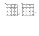
[表示例]
図9は、実施形態におけるディスクリネーションの発生態様を説明する図である。図9においては、表示パネル100の一定範囲の16個の画素110において、左半分の画素110には階調レベル「64」が指定され、右半分の画素110には階調レベル「65」が指定された場合の表示例を示す。図9(a)は、従来例のように、LUTを使い分けない場合、例えば、LUT(A)31のみを参照して画素110が駆動されている場合を示している。図中の「64」、「65」は、各画素110に指定された階調レベルを示している。図9(b)は、本発明の実施形態のように、画素110AはLUT(A)31を参照して駆動され、画素110BはLUT(B)32を参照して駆動された場合を示している。図中の「64A」、「64B」は、階調レベルが「64」に指定された画素110A、110Bを示し、「65A」、「65B」は、階調レベルが「65」に指定された画素110A、110Bを示している。
[Display example]
FIG. 9 is a diagram for explaining the occurrence of disclination in the embodiment. In FIG. 9, among the 16
従来例においては、図9(a)に示すように、階調レベル「64」と「65」との境界においては、Dリスクが高くなり、直線状のディスクリネーションDAが発生する。一方、本発明の実施形態においては、図9(b)に示すように、「64B」と「65A」との境界、および「65A」と「65B」との境界においてディスクリネーションDAが発生する。このように、本発明の実施形態においては、従来例に比べて、隣接階調レベルとなる部分に集中していたディスクリネーションDAを空間的に拡散することにより、目立たなくして表示への影響を低減することができる。 In the conventional example, as shown in FIG. 9A, the D risk increases at the boundary between the gradation levels “64” and “65”, and a linear disclination DA is generated. On the other hand, in the embodiment of the present invention, as shown in FIG. 9B, the disclination DA occurs at the boundary between “64B” and “65A” and the boundary between “65A” and “65B”. . As described above, in the embodiment of the present invention, compared to the conventional example, the disclination DA concentrated on the adjacent gradation level portion is spatially diffused to make the display inconspicuous and affect the display. Can be reduced.
また、図9(b)に示すように、階調レベルが「65」に指定された領域(特定の階調レベルに指定された領域)においては、ほぼ全域にわたってディスクリネーションDAが発生するため、ディスクリネーションDAが発生しない場合に比べて透過率が減少する。ここで、上述したように、一方のLUTにおける最大重み変化部となる階調レベルに対応するSFコードのうち「1」のビットとなる最も長い時間のサブフィールドにおいて、他方のLUTにおける同一の階調レベルに対応するSFコードのビットが「0」となる場合、すなわち、特定の階調レベルにおいては、合計オン時間が長くなるように規定されている。図8にも示したように、階調レベル「65」は、合計オン時間が長くなるように規定される対象であるから、ディスクリネーションDAの発生により減少した透過率を合計オン時間の増加により相殺して、本来の階調レベルに近い透過率として表示させることができる。 Further, as shown in FIG. 9B, the disclination DA is generated over almost the entire area in the area where the gradation level is designated as “65” (the area designated as the specific gradation level). The transmittance decreases compared to the case where no disclination DA occurs. Here, as described above, in the SF field corresponding to the gradation level which is the maximum weight change part in one LUT, in the subfield of the longest time which is “1” bits, the same floor in the other LUT is used. When the bit of the SF code corresponding to the tone level is “0”, that is, at a specific tone level, the total on-time is specified to be long. As shown in FIG. 8, the gradation level “65” is an object that is specified to increase the total on-time, and therefore the transmittance decreased due to the occurrence of the disclination DA is increased in the total on-time. Therefore, it is possible to display the transmittance close to the original gradation level.
<変形例>
以上、本発明の実施形態について説明したが、本発明は以下のように、さまざまな態様で実施可能である。
<Modification>
As mentioned above, although embodiment of this invention was described, this invention can be implemented in various aspects as follows.
[変形例1]
上述した実施形態において、1フレーム毎に画素110を駆動する際に参照するLUTを切り替えるようにしてもよい。この場合には、画素110Aと画素110Bとの位置関係が1フレーム毎に変化するようにSFコード変換部13は、参照するLUTを決定すればよい。
[Modification 1]
In the above-described embodiment, the LUT that is referred to when the
図10は、変形例1におけるディスクリネーションの発生態様を説明する図である。図10(a)は、奇数番目のフレームにおけるディスクリネーションDAの発生態様であり、図10(b)は、偶数番目のフレームにおけるディスクリネーションDAの発生態様である。このように、フレーム毎にディスクリネーションDAの位置が変化し、時間的にも拡散されることにより目立たなくすることで表示への影響を低減することができる。
なお、1フレーム毎に切り替えるのではなく、複数フレーム毎に切り替えるようにしてもよい。
FIG. 10 is a diagram for explaining the occurrence of disclination in the first modification. FIG. 10A shows a manner of occurrence of disclination DA in odd-numbered frames, and FIG. 10B shows a manner of occurrence of disclination DA in even-numbered frames. In this way, the position of the disclination DA changes from frame to frame, and the influence on the display can be reduced by making it inconspicuous by spreading over time.
Instead of switching every frame, it may be switched every plural frames.
[変形例2]
上述した実施形態においては、画素110Aと画素110Bとは図6に示すように、市松状に配置されていたが、別の態様で配置されていてもよい。
[Modification 2]
In the above-described embodiment, the pixels 110A and the pixels 110B are arranged in a checkered pattern as shown in FIG. 6, but may be arranged in another manner.
図11は、変形例2における各画素110に適用されるLUTを説明する図である。図11(a)に示すように、LUT(A)31が適用される画素110Aと、LUT(B)32が適用される画素110Bとは、それぞれ同数での配置に限らず、いずれかが多く配置されていてもよい。すなわち、少なくとも1つの画素110が他の画素110と異なるLUTが適用されるようになっていればよい。また、図11(b)に示すように、画素110Aと画素110Bとは、ランダムに配置されていてもよい。このとき、一定範囲における画素110Aと画素110Bの数が同数になるように配置されていてもよい。
このように、画素110Aと画素110Bとが分散配置され、ディスクリネーションが空間的に拡散するようになっていればよい。
FIG. 11 is a diagram for explaining an LUT applied to each
In this way, it is only necessary that the pixels 110A and the pixels 110B are distributed and the disclination is spatially diffused.
[変形例3]
上述した実施形態においては、LUT(A)31の最大重み変化部とLUT(B)32の最大重み変化部とは、隣接した階調レベルになっていたが、2以上離れた階調レベルに決められていてもよい。
[Modification 3]
In the above-described embodiment, the maximum weight change unit of the LUT (A) 31 and the maximum weight change unit of the LUT (B) 32 are adjacent gradation levels, but the gradation levels are separated by two or more. It may be decided.
[変形例4]
上述した実施形態においては、LUTは、LUT(A)31とLUT(B)32との2つのLUTを用いていたが、3以上のLUTを用いてもよい。
[Modification 4]
In the above-described embodiment, two LUTs of the LUT (A) 31 and the LUT (B) 32 are used as the LUT. However, three or more LUTs may be used.
[変形例5]
上述した実施形態においては、1フレームは、8のサブフィールドを1周期とした4つのブロックにより構成されていたが、これに限られず、より多くのブロックにより構成されていてもよいし、1つのブロックで構成されていてもよい。ここで、LUTによって規定されているSFコードが複数のブロックのサブフィールドについて、SFコードとして規定されている場合には、実施形態においても示されているように、階調レベルが隣接する高い側の階調レベルに変化したときに、各ブロックにおける長い時間のサブフィールドが同時にオフからオンに変化しないようにしてもよい。このようにすると、Dリスクを減少させディスクリネーションの表示に与える影響を低減することもできる。
[Modification 5]
In the above-described embodiment, one frame is composed of four blocks each having eight subfields as one period. However, the present invention is not limited to this, and may be composed of more blocks. It may be composed of blocks. Here, when the SF code defined by the LUT is defined as the SF code for the sub-fields of a plurality of blocks, as shown in the embodiment, the higher gradation level is adjacent. When the gradation level is changed, a long time subfield in each block may not be changed from OFF to ON at the same time. In this way, it is possible to reduce the D risk and reduce the influence on the display of the disclination.
[変形例6]
上述する実施形態においては、1フレームは、32のサブフィールドにより構成されていたが、この数に限られない。また、LUTにより規定されているSFコードは、16ビットであったが、このビット数に限られるものではない。
[Modification 6]
In the above-described embodiment, one frame is composed of 32 subfields, but is not limited to this number. The SF code defined by the LUT is 16 bits, but is not limited to this number of bits.
[変形例7]
上述する実施形態においては、表示パネル100は透過型であったが、反射型であってもよい。さらに、ノーマリーブラックモードでの駆動に限られず、ノーマリーホワイトモードでの駆動であってもよい。ここで、ノーマリーホワイトモードでの駆動としたとき、オンレベルとは、液晶素子120に電圧を印加して暗状態にさせるデータ信号をいい、オフレベルとは、液晶素子120を明状態にさせるデータ信号をいう。なお、ノーマリーホワイトモードでの駆動とした場合には、上記LUTのSFコードについて各ビットの「1」と「0」とを反転させればよい。すなわち、実施形態(ノーマリーブラックモード)における明状態の時間であるオン時間は、ノーマリーホワイトモードにおける明状態の時間は、オフ時間に対応する。ただし、単に各ビットの「1」、「0」を反転させるのではなく、以下の点については、SFコードの内容が変化する。
[Modification 7]
In the embodiment described above, the display panel 100 is a transmissive type, but may be a reflective type. Further, the driving is not limited to the normally black mode, but may be the driving in the normally white mode. Here, when driving in a normally white mode, the on level refers to a data signal that applies a voltage to the
横電界の影響により、画素に対して十分なオン電圧が印加されないことで、ディスクリネーションが発生する。したがって、ノーマリーホワイトモードにおいてディスクリネーションが発生した場合には、ディスクリネーションが発生しない場合と比較して透過率が増加する。そのため、一定範囲の画素110に特定の階調レベルが指定された場合に生じるディスクリネーションに起因して増加した透過率については、ノーマリーブラックモードと同様にして相殺すればよい。すなわち、実施形態に示したノーマリーブラックモードの場合、特定の階調レベルにおいて、合計オン時間を増加させて明状態となる時間を増加させ、ディスクリネーションに起因する透過率の減少分を相殺していた。一方、ノーマリーホワイトモードの場合、特定の階調レベルにおいて、合計オン時間を増加させて暗状態となる時間を増加させ、ディスクリネーションに起因する透過率の増加分を相殺すればよい。このようにして、ノーマリーホワイトモードであっても、本来の階調レベルに近い透過率として表示させることができる。
Disclination occurs because a sufficient on-voltage is not applied to the pixel due to the influence of the lateral electric field. Therefore, when disclination occurs in the normally white mode, the transmittance increases as compared to the case where disclination does not occur. Therefore, the transmittance increased due to disclination that occurs when a specific gradation level is designated for a certain range of
[変形例8]
上述した実施形態においては、1ブロックにおけるサブフィールドの時間はそれぞれ異なるものとなっていたが、その一部が同じ時間であってもよく、少なくとも1つのサブフィールドの時間が、他のサブフィールドの時間と異なる長さであればよい。
[Modification 8]
In the above-described embodiment, the subfield times in one block are different from each other, but some of them may be the same time, and the time of at least one subfield is the same as that of other subfields. It may be a length different from the time.
[変形例9]
上述する実施形態においては、表示パネル100は、プロジェクター2000に用いられる構成として説明したが、直視型の液晶ディスプレイに用いられてもよい。すなわち、液晶素子を用いた電気光学装置として機能するものであれば、どのようなものにも適用可能である。また、この電気光学装置を様々な電子機器に用いることもできる。電子機器としては、テレビジョンや、ビューファインダー型・モニタ直視型のビデオテープレコーダー、カーナビゲーション装置、ページャー、電子手帳、電卓、ワードプロセッサー、ワークステーション、テレビ電話、POS端末、デジタルスチルカメラ、携帯電話機、タッチパネルを備えた機器等などが挙げられる。
[Modification 9]
In the above-described embodiment, the display panel 100 has been described as a configuration used in the
10…コントローラー、11…タイミング制御回路、12…画質調整部、13…SFコード変換部、14…メモリー制御部、15…メモリー、16R,16G,16B…駆動回路、100R,100G,100B…表示パネル、105…液晶、108…コモン電極、110…画素、112…走査線、114…データ線、115…容量線、116…TFT、118…画素電極、120…液晶素子、125…補助容量、161…走査線駆動回路、162…データ線駆動回路、2000…プロジェクター、220…ランプユニット、2301…ダイクロイックミラー、2302…ミラー、2303…第1マルチレンズ、2304…第2マルチレンズ、2305…偏光変換素子、2306…重畳レンズ、2307…レンズ、2308…集光レンズ、240…ダイクロイックプリズム、250…投射レンズ、260…検出部、3000…スクリーン
DESCRIPTION OF
Claims (9)
前記画素に対して指定される階調レベルに応じて、1フレームを分割したサブフィールド毎に当該画素を明状態または暗状態に駆動する駆動部と
を具備し、
1フレームにおける少なくとも一の前記サブフィールドの時間は他の前記サブフィールドの時間とは異なり、
前記駆動部は、前記複数の画素に特定の階調レベルが指定された場合に、少なくとも一の前記画素と、当該一の画素に隣接する前記画素とは1フレーム中の駆動内容が異なるように、前記画素を駆動し、
前記特定の階調レベルは、
隣接する暗い側の階調レベルから当該特定の階調レベルに変化した場合において、前記一の画素の前記駆動内容が、暗状態から明状態に変化したサブフィールドのうち最も長い時間のサブフィールドと、変化後の当該駆動内容が明状態であるサブフィールドのうち最も長い時間のサブフィールドとが一致する関係を満たし、前記隣接する画素の前記駆動内容が、当該関係を満たさない階調レベルを示す
ことを特徴とする電気光学装置。 A plurality of pixels each having a liquid crystal element;
A driving unit that drives the pixel to a bright state or a dark state for each subfield divided into one frame according to a gradation level designated for the pixel;
The time of at least one subfield in one frame is different from the time of other subfields,
When the specific gradation level is designated for the plurality of pixels, the driving unit is configured such that at least one of the pixels and the pixel adjacent to the one pixel have different driving contents in one frame. Driving the pixel;
The specific gradation level is:
When the adjacent dark side gradation level changes to the specific gradation level, the drive content of the one pixel is the subfield of the longest time among the subfields that have changed from the dark state to the bright state. The drive content after the change satisfies the relationship in which the subfield of the longest time among the subfields in the bright state matches, and the drive content of the adjacent pixels indicates a gray level that does not satisfy the relationship An electro-optical device.
前記画素に対して指定される階調レベルに応じて、1フレームを分割したサブフィールド毎に当該画素を明状態または暗状態に駆動する駆動部と
を具備し、
1フレームにおける少なくとも一の前記サブフィールドの時間は他の前記サブフィールドの時間とは異なり、
前記駆動部は、前記複数の画素に特定の階調レベルが指定された場合に、少なくとも一の前記画素と、当該一の画素に隣接する前記画素とは1フレーム中の駆動内容が異なるように、前記画素を駆動し、
前記特定の階調レベルは、
隣接する暗い側の階調レベルから当該特定の階調レベルに変化した場合において、前記一の画素の前記駆動内容が、変化後の当該駆動内容が明状態であるサブフィールドの時間の合計に対する前記駆動内容が変化したサブフィールドの時間の合計の割合が予め決められた割合以上になる関係を満たし、前記隣接する画素の前記駆動内容が、当該関係を満たさない階調レベルを示す
ことを特徴とする電気光学装置。 A plurality of pixels each having a liquid crystal element;
A driving unit that drives the pixel to a bright state or a dark state for each subfield divided into one frame according to a gradation level designated for the pixel;
The time of at least one subfield in one frame is different from the time of other subfields,
When the specific gradation level is designated for the plurality of pixels, the driving unit is configured such that at least one of the pixels and the pixel adjacent to the one pixel have different driving contents in one frame. Driving the pixel;
The specific gradation level is:
When the adjacent dark side gradation level changes to the specific gradation level, the drive content of the one pixel is the sum of the times of the subfields in which the drive content after the change is in the bright state. The ratio of the total time of the subfields in which the driving contents are changed satisfies a relationship that is equal to or higher than a predetermined ratio, and the driving contents of the adjacent pixels indicate a gray level that does not satisfy the relationship. An electro-optical device.
前記特定の階調レベルにおける1フレーム中の明状態の時間は、当該階調レベルに隣接する暗い側と明るい側との階調レベルにおける1フレーム中の明状態の時間の平均よりも長くなるように決められている
ことを特徴とする請求項1または請求項2に記載の電気光学装置。 The liquid crystal element is driven in a normally black mode,
The light state time in one frame at the specific gradation level is longer than the average of the light state times in one frame at the dark side and bright side adjacent to the gradation level. The electro-optical device according to claim 1, wherein the electro-optical device is defined as follows.
前記特定の階調レベルにおける1フレーム中の明状態の時間は、当該階調レベルに隣接する暗い側と明るい側との階調レベルにおける1フレーム中の明状態の時間の平均よりも短くなるように決められている
ことを特徴とする請求項1または請求項2に記載の電気光学装置。 The liquid crystal element is driven in a normally white mode,
The light state time in one frame at the specific gradation level is shorter than the average of the light state times in one frame at the dark side and bright side adjacent to the gradation level. The electro-optical device according to claim 1, wherein the electro-optical device is defined as follows.
前記特定の階調レベルにおける1フレーム中の明状態の時間は、当該階調レベルに隣接する明るい側の階調レベルにおける1フレーム中の明状態の時間よりも長くなるように決められている
ことを特徴とする請求項1または請求項2に記載の電気光学装置。 The liquid crystal element is driven in a normally black mode,
The light state time in one frame at the specific gradation level is determined to be longer than the light state time in one frame at the bright gradation level adjacent to the gradation level. The electro-optical device according to claim 1 or 2.
前記特定の階調レベルにおける1フレーム中の明状態の時間は、当該階調レベルに隣接する暗い側の階調レベルにおける1フレーム中の明状態の時間よりも短くなるように決められている
ことを特徴とする請求項1または請求項2に記載の電気光学装置。 The liquid crystal element is driven in a normally white mode,
The light state time in one frame at the specific gradation level is determined to be shorter than the light state time in one frame at the dark gradation level adjacent to the gradation level. The electro-optical device according to claim 1 or 2.
ことを特徴とする請求項1乃至請求項6のいずれかに記載の電気光学装置。 The drive unit drives the pixel so that the position of the at least one pixel in the plurality of pixels is changed every frame or every plurality of frames. An electro-optical device according to claim 1.
ことを特徴とする請求項1乃至請求項7のいずれかに記載の電気光学装置。 The driving unit drives all the pixels so that the driving contents in one frame are different from those of the adjacent pixels when the specific gradation level is designated for the plurality of pixels. The electro-optical device according to claim 1, wherein the electro-optical device is any one of claims 1 to 7.
ことを特徴とする請求項1乃至請求項8のいずれかに記載の電気光学装置。 When the specific gradation level is specified for the plurality of pixels, the driving unit determines a difference between a light state time in the at least one pixel and a light state time in the adjacent pixels. The electro-optical device according to any one of claims 1 to 8, wherein the pixel is driven so as to be within 10% of a sum of the above.
Priority Applications (3)
| Application Number | Priority Date | Filing Date | Title |
|---|---|---|---|
| JP2011091941A JP2012226041A (en) | 2011-04-18 | 2011-04-18 | Electro-optic device |
| CN201210103677.9A CN102750917B (en) | 2011-04-18 | 2012-04-10 | Electrooptical device |
| US13/446,824 US9058767B2 (en) | 2011-04-18 | 2012-04-13 | Electrooptical device having pixel subfields controllable to produce gray levels |
Applications Claiming Priority (1)
| Application Number | Priority Date | Filing Date | Title |
|---|---|---|---|
| JP2011091941A JP2012226041A (en) | 2011-04-18 | 2011-04-18 | Electro-optic device |
Publications (1)
| Publication Number | Publication Date |
|---|---|
| JP2012226041A true JP2012226041A (en) | 2012-11-15 |
Family
ID=47006100
Family Applications (1)
| Application Number | Title | Priority Date | Filing Date |
|---|---|---|---|
| JP2011091941A Pending JP2012226041A (en) | 2011-04-18 | 2011-04-18 | Electro-optic device |
Country Status (3)
| Country | Link |
|---|---|
| US (1) | US9058767B2 (en) |
| JP (1) | JP2012226041A (en) |
| CN (1) | CN102750917B (en) |
Cited By (7)
| Publication number | Priority date | Publication date | Assignee | Title |
|---|---|---|---|---|
| JP2014153595A (en) * | 2013-02-12 | 2014-08-25 | Seiko Epson Corp | Video processing circuit, video processing method and electronic equipment |
| JP2015038558A (en) * | 2013-08-19 | 2015-02-26 | セイコーエプソン株式会社 | DRIVE DEVICE, DISPLAY DEVICE, ELECTRONIC DEVICE, AND DRIVE METHOD |
| JP2016004103A (en) * | 2014-06-16 | 2016-01-12 | セイコーエプソン株式会社 | Electro-optic device, method for driving electro-optic device, and electronic apparatus |
| US10163382B2 (en) | 2015-09-08 | 2018-12-25 | Canon Kabushiki Kaisha | Liquid crystal drive apparatus, image display apparatus capable of reducing degradation in image quality due to disclination, and storage medium storing liquid crystal drive program capable thereof |
| US10198985B2 (en) | 2015-09-08 | 2019-02-05 | Canon Kabushiki Kaisha | Liquid crystal drive apparatus, image display apparatus and storage medium storing liquid crystal drive program |
| US10229625B2 (en) | 2015-09-08 | 2019-03-12 | Canon Kabushiki Kaisha | Liquid crystal drive apparatus, image display apparatus and storage medium storing liquid crystal drive program |
| US10304371B2 (en) | 2015-09-08 | 2019-05-28 | Canon Kabushiki Kaisha | Liquid crystal drive apparatus, image display apparatus and storage medium storing liquid crystal drive program |
Citations (1)
| Publication number | Priority date | Publication date | Assignee | Title |
|---|---|---|---|---|
| JP2008051949A (en) * | 2006-08-23 | 2008-03-06 | Fujitsu Hitachi Plasma Display Ltd | Gradation display processing method and plasma display device |
Family Cites Families (11)
| Publication number | Priority date | Publication date | Assignee | Title |
|---|---|---|---|---|
| JP3918536B2 (en) | 2000-11-30 | 2007-05-23 | セイコーエプソン株式会社 | Electro-optical device driving method, driving circuit, electro-optical device, and electronic apparatus |
| JP4023517B2 (en) | 2000-11-30 | 2007-12-19 | セイコーエプソン株式会社 | Electro-optical device, drive circuit, and electronic apparatus |
| JP4020158B2 (en) | 2000-11-30 | 2007-12-12 | セイコーエプソン株式会社 | Electro-optical device, drive circuit, and electronic apparatus |
| JP3888076B2 (en) | 2001-03-28 | 2007-02-28 | セイコーエプソン株式会社 | Electro-optical device driving method, electro-optical device driving device, electro-optical device, and electronic apparatus |
| JP2003177723A (en) * | 2001-12-11 | 2003-06-27 | Seiko Epson Corp | Electro-optical device driving method, driving circuit, electro-optical device, and electronic apparatus |
| JP4172250B2 (en) * | 2002-11-01 | 2008-10-29 | セイコーエプソン株式会社 | Electro-optical device, driving method of electro-optical device, and electronic apparatus |
| JP5056203B2 (en) * | 2007-06-28 | 2012-10-24 | セイコーエプソン株式会社 | Electro-optical device, driving method thereof, and electronic apparatus |
| JP5446328B2 (en) * | 2009-03-06 | 2014-03-19 | セイコーエプソン株式会社 | Display device, electronic device, and drive code generation circuit |
| JP2011059610A (en) | 2009-09-14 | 2011-03-24 | Seiko Epson Corp | Electro-optical device, driving method thereof, and electronic apparatus |
| JP2011064752A (en) | 2009-09-15 | 2011-03-31 | Seiko Epson Corp | Electro-optical device, method for driving the same, and electronic equipment |
| JP5720110B2 (en) * | 2010-04-08 | 2015-05-20 | セイコーエプソン株式会社 | Electro-optical device, control method of electro-optical device, and electronic apparatus |
-
2011
- 2011-04-18 JP JP2011091941A patent/JP2012226041A/en active Pending
-
2012
- 2012-04-10 CN CN201210103677.9A patent/CN102750917B/en not_active Expired - Fee Related
- 2012-04-13 US US13/446,824 patent/US9058767B2/en not_active Expired - Fee Related
Patent Citations (1)
| Publication number | Priority date | Publication date | Assignee | Title |
|---|---|---|---|---|
| JP2008051949A (en) * | 2006-08-23 | 2008-03-06 | Fujitsu Hitachi Plasma Display Ltd | Gradation display processing method and plasma display device |
Cited By (7)
| Publication number | Priority date | Publication date | Assignee | Title |
|---|---|---|---|---|
| JP2014153595A (en) * | 2013-02-12 | 2014-08-25 | Seiko Epson Corp | Video processing circuit, video processing method and electronic equipment |
| JP2015038558A (en) * | 2013-08-19 | 2015-02-26 | セイコーエプソン株式会社 | DRIVE DEVICE, DISPLAY DEVICE, ELECTRONIC DEVICE, AND DRIVE METHOD |
| JP2016004103A (en) * | 2014-06-16 | 2016-01-12 | セイコーエプソン株式会社 | Electro-optic device, method for driving electro-optic device, and electronic apparatus |
| US10163382B2 (en) | 2015-09-08 | 2018-12-25 | Canon Kabushiki Kaisha | Liquid crystal drive apparatus, image display apparatus capable of reducing degradation in image quality due to disclination, and storage medium storing liquid crystal drive program capable thereof |
| US10198985B2 (en) | 2015-09-08 | 2019-02-05 | Canon Kabushiki Kaisha | Liquid crystal drive apparatus, image display apparatus and storage medium storing liquid crystal drive program |
| US10229625B2 (en) | 2015-09-08 | 2019-03-12 | Canon Kabushiki Kaisha | Liquid crystal drive apparatus, image display apparatus and storage medium storing liquid crystal drive program |
| US10304371B2 (en) | 2015-09-08 | 2019-05-28 | Canon Kabushiki Kaisha | Liquid crystal drive apparatus, image display apparatus and storage medium storing liquid crystal drive program |
Also Published As
| Publication number | Publication date |
|---|---|
| US9058767B2 (en) | 2015-06-16 |
| US20120262501A1 (en) | 2012-10-18 |
| CN102750917A (en) | 2012-10-24 |
| CN102750917B (en) | 2014-10-22 |
Similar Documents
| Publication | Publication Date | Title |
|---|---|---|
| JP3918536B2 (en) | Electro-optical device driving method, driving circuit, electro-optical device, and electronic apparatus | |
| JP5720110B2 (en) | Electro-optical device, control method of electro-optical device, and electronic apparatus | |
| JP4349433B2 (en) | Electro-optical device, driving circuit thereof, driving method, and electronic apparatus | |
| JP5056203B2 (en) | Electro-optical device, driving method thereof, and electronic apparatus | |
| JP4349434B2 (en) | Electro-optical device, driving circuit thereof, driving method, and electronic apparatus | |
| CN102750917B (en) | Electrooptical device | |
| US8531369B2 (en) | Electro-optic device and electronic apparatus | |
| JP2010191038A (en) | Driving method for liquid crystal display, the liquid crystal display, and electronic device | |
| JP2020052132A (en) | Electro-optical device and control method therefor | |
| US8212800B2 (en) | Electro-optic device, driving method, and electronic apparatus | |
| KR100501622B1 (en) | Driving method of electrooptical apparatus, driving circuit and electrooptical apparatus, and electronic device | |
| JP5082579B2 (en) | Electro-optical device, driving method thereof, and electronic apparatus | |
| JP5798707B2 (en) | Image display device, control method thereof, and electronic apparatus | |
| JP2008185993A (en) | Electro-optical device, processing circuit, processing method, and projector | |
| JP4020158B2 (en) | Electro-optical device, drive circuit, and electronic apparatus | |
| JP2011059610A (en) | Electro-optical device, driving method thereof, and electronic apparatus | |
| JP2011064752A (en) | Electro-optical device, method for driving the same, and electronic equipment | |
| JP2020064103A (en) | Method for driving electro-optical device, electro-optical device, and electronic apparatus | |
| JP5682243B2 (en) | Electro-optical device, driving method of electro-optical device, and electronic apparatus | |
| JP6102992B2 (en) | Image display device, control method thereof, and electronic apparatus | |
| JP4023517B2 (en) | Electro-optical device, drive circuit, and electronic apparatus | |
| JP2010271529A (en) | Electro-optical device, driving method thereof, and electronic apparatus | |
| JP5194735B2 (en) | Electro-optical device, driving method thereof, and electronic apparatus | |
| JP2015038558A (en) | DRIVE DEVICE, DISPLAY DEVICE, ELECTRONIC DEVICE, AND DRIVE METHOD | |
| JP2010186038A (en) | Electrooptical apparatus, driving method thereof, and electronic device |
Legal Events
| Date | Code | Title | Description |
|---|---|---|---|
| A621 | Written request for application examination |
Free format text: JAPANESE INTERMEDIATE CODE: A621 Effective date: 20140326 |
|
| A977 | Report on retrieval |
Free format text: JAPANESE INTERMEDIATE CODE: A971007 Effective date: 20150107 |
|
| A131 | Notification of reasons for refusal |
Free format text: JAPANESE INTERMEDIATE CODE: A131 Effective date: 20150217 |
|
| A521 | Written amendment |
Free format text: JAPANESE INTERMEDIATE CODE: A523 Effective date: 20150420 |
|
| A02 | Decision of refusal |
Free format text: JAPANESE INTERMEDIATE CODE: A02 Effective date: 20150929 |