JP2012209488A - Light-emitting device - Google Patents

Light-emitting device Download PDF

Info

Publication number
JP2012209488A
JP2012209488A JP2011075192A JP2011075192A JP2012209488A JP 2012209488 A JP2012209488 A JP 2012209488A JP 2011075192 A JP2011075192 A JP 2011075192A JP 2011075192 A JP2011075192 A JP 2011075192A JP 2012209488 A JP2012209488 A JP 2012209488A
Authority
JP
Japan
Prior art keywords
layer
gallium nitride
light
semiconductor layer
light emitting
Prior art date
Legal status (The legal status is an assumption and is not a legal conclusion. Google has not performed a legal analysis and makes no representation as to the accuracy of the status listed.)
Withdrawn
Application number
JP2011075192A
Other languages
Japanese (ja)
Inventor
Hiroyasu Tanaka
浩康 田中
Current Assignee (The listed assignees may be inaccurate. Google has not performed a legal analysis and makes no representation or warranty as to the accuracy of the list.)
Kyocera Corp
Original Assignee
Kyocera Corp
Priority date (The priority date is an assumption and is not a legal conclusion. Google has not performed a legal analysis and makes no representation as to the accuracy of the date listed.)
Filing date
Publication date
Application filed by Kyocera Corp filed Critical Kyocera Corp
Priority to JP2011075192A priority Critical patent/JP2012209488A/en
Publication of JP2012209488A publication Critical patent/JP2012209488A/en
Withdrawn legal-status Critical Current

Links

Images

Abstract

PROBLEM TO BE SOLVED: To provide a light-emitting device that can hardly cause reduction in the light-emitting efficiency while improving the crystallinity of an optical semiconductor layer.SOLUTION: A light-emitting device of the present invention comprises: an n-type gallium nitride-based semiconductor layer 3; a light-emitting layer 4 that is provided on the n-type gallium nitride-based semiconductor layer 3 and contains a gallium nitride-based semiconductor; and a p-type gallium nitride-based semiconductor layer 6 that is provided on the light-emitting layer 4 and has a blocking layer 5 contacting the light-emitting layer 4. The blocking layer 5 is formed by stacking electron blocking layers 5a that contain magnesium and hole tunneling layers 5b that have a lower magnesium concentration than the electron blocking layers 5a and have a thickness of 3 nm or less. Since the blocking layer 5 has such the hole tunneling layers 5b, reduction in the light-emitting efficiency can be hardly caused while improving the crystallinity of an optical semiconductor layer 7.

Description

本発明は、半導体を複数積層させた発光素子に関するものである。   The present invention relates to a light emitting element in which a plurality of semiconductors are stacked.

現在、紫外光、青色光あるいは緑色光等を発光する発光素子として、n型半導体層、発光層およびp型半導体層を順次積層させた光半導体層が種々提案されている。特に、光半導体層を構成する光半導体として窒化物半導体を用いた発光素子の開発において、発光素子の発光効率を向上させることが必要となっている。   At present, various types of optical semiconductor layers in which an n-type semiconductor layer, a light-emitting layer, and a p-type semiconductor layer are sequentially stacked have been proposed as light-emitting elements that emit ultraviolet light, blue light, green light, or the like. In particular, in the development of a light emitting element using a nitride semiconductor as the optical semiconductor constituting the optical semiconductor layer, it is necessary to improve the light emission efficiency of the light emitting element.

発光素子の発光効率を向上させる技術として、n型半導体層から発光層へ注入される電子が発光層を越えてp型半導体層内に入ることを抑制するブロック層を発光層とp型半導体層との間に設ける技術が開示されている(例えば、特許文献1参照)。   As a technique for improving the light emission efficiency of a light-emitting element, a light-emitting layer and a p-type semiconductor layer include a block layer that suppresses electrons injected from the n-type semiconductor layer into the light-emitting layer from entering the p-type semiconductor layer. (See, for example, Patent Document 1).

特開2000−91631号公報JP 2000-91631 A

しかしながら、特許文献1に記載された発光素子によれば、ブロック層は、p型半導体層内において他のp型半導体層よりもマグネシウムの含有量を大きくして設ける必要があったため、ブロック層の結晶品質が低下してしまい、ブロック層上に積層されるp型半導体層の結晶品質を向上させることが困難だった。   However, according to the light emitting element described in Patent Document 1, the block layer needs to be provided with a magnesium content larger than that of other p-type semiconductor layers in the p-type semiconductor layer. The crystal quality deteriorates, and it is difficult to improve the crystal quality of the p-type semiconductor layer stacked on the block layer.

本発明は上記課題に鑑みてなされたものであり、その目的は、半導体層の結晶性を向上させつつ、発光効率の低下を招きにくくすることが可能な発光素子を提供することにある。   The present invention has been made in view of the above problems, and an object of the present invention is to provide a light emitting element capable of improving the crystallinity of a semiconductor layer and hardly causing a decrease in light emission efficiency.

本発明の発光素子は、n型窒化ガリウム系半導体層と、該n型窒化ガリウム系半導体層上に設けられた、窒化ガリウム系半導体を含む発光層と、該発光層上に設けられた、該発光層と接するブロック層を持つp型窒化ガリウム系半導体層とを有し、前記ブロック層は、マグネシウムを含有した電子ブロック層と、該電子ブロック層よりもマグネシウムの含有量が小さい、厚みが3nm以下の正孔トンネル層とが積層されている。   The light emitting element of the present invention includes an n-type gallium nitride semiconductor layer, a light emitting layer including a gallium nitride semiconductor provided on the n type gallium nitride semiconductor layer, and the light emitting layer provided on the light emitting layer. A p-type gallium nitride based semiconductor layer having a block layer in contact with the light emitting layer, wherein the block layer has an electron block layer containing magnesium, a magnesium content smaller than the electron block layer, and a thickness of 3 nm The following hole tunnel layers are stacked.

本発明の発光素子によれば、上記の通り、ブロック層が電子ブロック層と電子ブロック層よりもマグネシウムの含有量が小さい正孔トンネル層とで構成されていることから、ブロック層の結晶品質を向上させることができる。また、マグネシウムの含有量を小さくした正孔トンネル層の厚みが3nm以下となるように設定されていることから、p型半導体層内の正孔が正孔トンネル層の障壁を通過して発光層側に移動することができるようになり、発光素子の発光効率の低下を招きにくくすることができる。   According to the light emitting device of the present invention, as described above, the block layer is composed of the electron block layer and the hole tunnel layer having a lower magnesium content than the electron block layer. Can be improved. In addition, since the thickness of the hole tunnel layer with a reduced magnesium content is set to be 3 nm or less, the holes in the p-type semiconductor layer pass through the barrier of the hole tunnel layer and the light emitting layer It can move to the side, and it can be made hard to cause the fall of the luminous efficiency of a light emitting element.

本発明の発光素子の実施形態の一例を示す斜視図である。It is a perspective view which shows an example of embodiment of the light emitting element of this invention. 図1に示す発光素子の断面図であり、図1のA−A’線で切断したときの断面に相当する。FIG. 2 is a cross-sectional view of the light-emitting element shown in FIG. 1 and corresponds to a cross section taken along line A-A ′ of FIG. 1. 式のパラメータを説明するための模式図であり、ポテンシャル分布を表す図である。It is a schematic diagram for demonstrating the parameter of a type | formula, and is a figure showing potential distribution. 図1および図2に示す発光素子において、発光層、ブロック層およびp型窒化ガリウム系半導体層のエネルギーバンドを示すバンド図である。FIG. 3 is a band diagram showing energy bands of a light emitting layer, a block layer, and a p-type gallium nitride based semiconductor layer in the light emitting device shown in FIGS. 1 and 2. 本発明の発光素子の実施形態の変形例であり、発光層、ブロック層およびp型窒化ガリウム系半導体層のエネルギーバンドを示すバンド図である。It is a modification of embodiment of the light emitting element of this invention, and is a band figure which shows the energy band of a light emitting layer, a block layer, and a p-type gallium nitride semiconductor layer. 本発明の発光素子の実施形態の変形例であり、n型窒化ガリウム系半導体層、第2ブロック層および発光層のエネルギーバンドを示すバンド図である。It is a modification of embodiment of the light emitting element of this invention, and is a band figure which shows the energy band of an n-type gallium nitride semiconductor layer, a 2nd block layer, and a light emitting layer. 本発明の発光素子の製造方法の実施形態の一例の一工程を示す断面図である。It is sectional drawing which shows 1 process of an example of embodiment of the manufacturing method of the light emitting element of this invention. 本発明の発光素子の製造方法の実施形態の一例の一工程を示す断面図である。It is sectional drawing which shows 1 process of an example of embodiment of the manufacturing method of the light emitting element of this invention.

以下、本発明の実施の形態の例について図を参照しながら説明する。なお、本発明は以下の実施の形態の例に限定されるものではなく、本発明の要旨を逸脱しない範囲内で種々の変更を施すことができる。   Hereinafter, an example of an embodiment of the present invention will be described with reference to the drawings. In addition, this invention is not limited to the example of the following embodiment, A various change can be given in the range which does not deviate from the summary of this invention.

<発光素子>
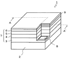
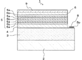
図1に、本発明の実施の形態の一例である発光素子1の斜視図を示す。図2は図1に示す発光素子1の断面図であり、図1のA−A’線で切断したときの断面に相当する。
<Light emitting element>
FIG. 1 shows a perspective view of a light-emitting element 1 which is an example of an embodiment of the present invention. 2 is a cross-sectional view of the light-emitting element 1 shown in FIG. 1, and corresponds to a cross section taken along line AA ′ of FIG.

発光素子1は、図1に示すように、主に、基板2と、n型窒化ガリウム系半導体層3、発光層4、ブロック層5およびp型窒化ガリウム系半導体層6からなる光半導体層7とを有している。   As shown in FIG. 1, the light-emitting element 1 includes an optical semiconductor layer 7 mainly composed of a substrate 2, an n-type gallium nitride semiconductor layer 3, a light-emitting layer 4, a block layer 5, and a p-type gallium nitride semiconductor layer 6. And have.

基板2は、光半導体層7を結晶成長させることが可能な材料を用いることができ、例えばサファイア、窒化ガリウム、窒化アルミニウム、ホウ化ジルコニウムまたは酸化亜鉛などの結晶性材料を用いることができる。このような基板2は、平面視形状が四角形状となるように形成されている。基板2の厚みは、例えば10μm以上1000μm以下に設定されている。なお、基板2の平面視形状としては、例えば四角形状もしくは五角形状などの多角形状または円形状などに設定することができる。   For the substrate 2, a material capable of crystal growth of the optical semiconductor layer 7 can be used. For example, a crystalline material such as sapphire, gallium nitride, aluminum nitride, zirconium boride, or zinc oxide can be used. Such a board | substrate 2 is formed so that planar view shape may become square shape. The thickness of the substrate 2 is set to, for example, 10 μm or more and 1000 μm or less. In addition, as a planar view shape of the board | substrate 2, it can set to polygonal shapes, such as square shape or pentagon shape, or circular shape, for example.

このような基板2は、後述する光半導体層7を成長させた後、エッチングなどを用いて除去してもよい。これにより、光半導体層7で発光した光が基板2で吸収されにくくなるため、光取り出し効率を向上させることができる。また、基板2が除去された光半導体層7の主面に凹凸構造を設けることにより、基板2が除去された光半導体層7の主面で全反射されにくくすることができ、光取り出し効率を向上させることができる。   Such a substrate 2 may be removed by etching or the like after growing an optical semiconductor layer 7 described later. Thereby, since the light emitted from the optical semiconductor layer 7 is not easily absorbed by the substrate 2, the light extraction efficiency can be improved. In addition, by providing a concavo-convex structure on the main surface of the optical semiconductor layer 7 from which the substrate 2 has been removed, it is possible to prevent total reflection from being performed on the main surface of the optical semiconductor layer 7 from which the substrate 2 has been removed. Can be improved.

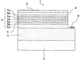
光半導体層7は、図2に示すように、基板2上に複数の半導体層を積層させることによって構成されている。光半導体層7の平面視形状は、基板2の平面視形状と同様に、例えば四角形状もしくは五角形状などの多角形状または円形状などとすることができる。光半導体層7は、全体の厚みが例えば100nm以上20μm以下で形成される。また、光半導体層7の各層の屈折率は、窒化ガリウムを用いた場合には、例えば1.80以上2.70以下に設定される。   As shown in FIG. 2, the optical semiconductor layer 7 is configured by laminating a plurality of semiconductor layers on the substrate 2. The planar view shape of the optical semiconductor layer 7 can be, for example, a polygonal shape such as a quadrangular shape or a pentagonal shape or a circular shape, like the planar view shape of the substrate 2. The optical semiconductor layer 7 is formed with an overall thickness of, for example, 100 nm or more and 20 μm or less. The refractive index of each layer of the optical semiconductor layer 7 is set to, for example, 1.80 or more and 2.70 or less when gallium nitride is used.

光半導体層7は、n型窒化ガリウム系半導体層3、窒化ガリウム系半導体を含む発光層4、ブロック層5およびp型窒化ガリウム系半導体層6から構成されている。窒化ガリウム系半導体は、例えばインジウム、アルミニウム、ボロンを含む窒化ガリウム半導体の混晶を用いることができる。なお、突起ガリウム系半導体として窒化ガリウムのみを用いて
もよい。
The optical semiconductor layer 7 includes an n-type gallium nitride based semiconductor layer 3, a light emitting layer 4 containing a gallium nitride based semiconductor, a block layer 5, and a p-type gallium nitride based semiconductor layer 6. As the gallium nitride semiconductor, a mixed crystal of a gallium nitride semiconductor containing, for example, indium, aluminum, and boron can be used. Note that only gallium nitride may be used as the protruding gallium semiconductor.

n型窒化ガリウム系半導体層3は、基板2上に設けられる。n型窒化ガリウム系半導体層3は、窒化ガリウムからなり、厚みが例えば50nm以上10μm以下に設定されている。n型窒化ガリウム系半導体層3は、例えば不純物としてシリコンを含ませることにより、電子を多数キャリアとするn型の導電型が半導体に付与されている。   The n-type gallium nitride based semiconductor layer 3 is provided on the substrate 2. The n-type gallium nitride based semiconductor layer 3 is made of gallium nitride and has a thickness of, for example, 50 nm or more and 10 μm or less. The n-type gallium nitride based semiconductor layer 3 includes, for example, silicon as an impurity, thereby imparting an n-type conductivity type with electrons as majority carriers to the semiconductor.

発光層4は、n型窒化ガリウム系半導体層3上に設けられる。発光層4には、禁制帯幅の広い障壁層と禁制帯幅の狭い井戸層とからなる量子井戸構造が複数回繰り返し規則的に積層された多層量子井戸構造(MQW)を用いることができる。障壁層と井戸層の一方は、窒化ガリウム系半導体から構成されている。障壁層および井戸層としては、インジウムとガリウムとの窒化物からなる混晶においてインジウムとガリウムとの組成比を調整したものを用いることができる。このように構成された発光層4は、例えば350nm以上600nm以下の波長で発光強度がピークとなる光を発光することができる。   The light emitting layer 4 is provided on the n-type gallium nitride based semiconductor layer 3. The light emitting layer 4 may be a multilayer quantum well structure (MQW) in which a quantum well structure including a barrier layer having a wide forbidden band and a well layer having a narrow forbidden band is regularly stacked a plurality of times. One of the barrier layer and the well layer is made of a gallium nitride based semiconductor. As the barrier layer and the well layer, a mixed crystal composed of a nitride of indium and gallium with the composition ratio of indium and gallium adjusted can be used. The light emitting layer 4 thus configured can emit light having a peak emission intensity at a wavelength of 350 nm or more and 600 nm or less, for example.

p型窒化ガリウム系半導体層6は、発光層4上に設けられる。p型窒化ガリウム系半導体層6は、発光層4と接するようにブロック層5を有している。p型窒化ガリウム系半導体層6は、例えば不純物としてマグネシウムを含ませることによって、正孔を多数キャリアとするp型の導電型が半導体に付与されている。なお、n型窒化ガリウム系半導体層3とp型窒化ガリウム系半導体層6とは、互いに逆に配置されていてもよい。   The p-type gallium nitride based semiconductor layer 6 is provided on the light emitting layer 4. The p-type gallium nitride based semiconductor layer 6 has a block layer 5 so as to be in contact with the light emitting layer 4. The p-type gallium nitride based semiconductor layer 6 is provided with a p-type conductivity type having holes as majority carriers, for example, by including magnesium as an impurity. Note that the n-type gallium nitride semiconductor layer 3 and the p-type gallium nitride semiconductor layer 6 may be disposed opposite to each other.

ブロック層5は、発光層4とp型窒化ガリウム系半導体層6との間に配置されている。ブロック層5は、電子ブロック層5aおよび正孔トンネル層5bが積層されて構成されている。本例においては、ブロック層5は、電子ブロック層5aと正孔トンネル層5bとの積層体が複数積層されている。   The block layer 5 is disposed between the light emitting layer 4 and the p-type gallium nitride based semiconductor layer 6. The block layer 5 is configured by laminating an electron block layer 5a and a hole tunnel layer 5b. In this example, the block layer 5 is formed by stacking a plurality of stacked bodies of an electron block layer 5a and a hole tunnel layer 5b.

電子ブロック層5aは、マグネシウムが含有するように設けられている。具体的に、電子ブロック層5aは、窒化ガリウム系半導体にマグネシウムがドープされることによって設けられる。窒化ガリウム系半導体は、マグネシウムの含有量がp型窒化ガリウム系半導体層6よりも高くなるように設定することができ、例えば1×10¹⁹/cm以上1×1020/cm以下となるように設定されている。電子ブロック層5aは、厚みが、例えば4nm以上0.5μm以下となるように設定することができる。 The electron block layer 5a is provided so as to contain magnesium. Specifically, the electron block layer 5a is provided by doping a gallium nitride semiconductor with magnesium. The gallium nitride semiconductor can be set so that the magnesium content is higher than that of the p-type gallium nitride semiconductor layer 6, for example, 1 × 10 19 / cm 3 or more and 1 × 10 20 / cm 3 or less. Is set to The electron blocking layer 5a can be set so that the thickness is, for example, 4 nm or more and 0.5 μm or less.

正孔トンネル層5bは、電子ブロック層5a上に積層されている。正孔トンネル層5bは、電子ブロック層5aよりもマグネシウムの含有量が小さくなるように設定されており、例えば電子ブロック層5aのマグネシウム含有量が正孔トンネル層5bのマグネシウム含有量よりも100分の1以下となるように設定することができる。具体的に、正孔トンネル層5bのマグネシウム含有量は、例えば1×10¹⁸/cm以下となるように設定することができる。正孔トンネル層5aは、層全体が電子ブロック層5aのマグネシウム含有量よりも小さくなるように設定されている。なお、電子ブロック層5aおよび正孔トンネル層5bのマグネシウム含有量は、例えば飛行時間型二次イオン質量分析(Time of Flight
Secondary Ion Mass Spectroscopy)法などを用いて分析することができる。
The hole tunnel layer 5b is stacked on the electron block layer 5a. The hole tunnel layer 5b is set so that the magnesium content is smaller than that of the electron block layer 5a. For example, the magnesium content of the electron block layer 5a is 100 minutes than the magnesium content of the hole tunnel layer 5b. Can be set to be 1 or less. Specifically, the magnesium content of the hole tunnel layer 5b can be set to be 1 × 10 18 / cm 3 or less, for example. The hole tunnel layer 5a is set so that the entire layer is smaller than the magnesium content of the electron block layer 5a. The magnesium content of the electron block layer 5a and the hole tunnel layer 5b is, for example, time-of-flight secondary ion mass spectrometry (Time of Flight
Secondary Ion Mass Spectroscopy) can be used for analysis.

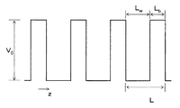
また、正孔トンネル層5bの厚みは、正孔が正孔トンネル層5bをトンネルして通過することができるように設定される。具体的には、窒化ガリウム系半導体にマグネシウムを添加することによりp型の導電型を付与した場合であれば、正孔トンネル層5bは、3nm以下となるように設定することができる。このような正孔トンネル層5bの厚みとしては、以下の式を用いて算出することができる。   The thickness of the hole tunnel layer 5b is set so that holes can pass through the hole tunnel layer 5b. Specifically, when the p-type conductivity is imparted by adding magnesium to the gallium nitride based semiconductor, the hole tunnel layer 5b can be set to 3 nm or less. The thickness of the hole tunnel layer 5b can be calculated using the following formula.

Figure 2012209488
Figure 2012209488

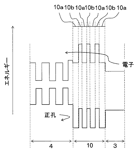
ここで、図4に式のモデルを示す。Lwは電子ブロック層5bの厚み、Lbは正孔トンネル層5aの厚みを用いることができ、Lは電子ブロック層5bと正孔トンネル層5bとの積層体がz方向に複数積層された際の周期を示している。また、Vは正孔トンネル層5bの電子ブロック層5aに対するエネルギー障壁を表しており、例えば接合前の電子ブロック層5aおよび正孔トンネル層5bのフェルミエネルギーの差の値を用いることができる。mは正孔トンネル層5bにおける正孔の有効質量を示しており、例えば自由電子の質量を1倍から2倍したものを用いることができる。さらに、hはプランク定数、kは波数であり、Ezはその波数に対するエネルギーを示している。なお、このような値を上記の式に当て嵌めて解くと、正孔がトンネルすることのできる正孔トンネル層5bの厚みは、3nm以下となる。また、電子ブロック層5aの厚みに関しても、電子をトンネルさせない厚みを同様の式を用いて算出することができる。 Here, FIG. 4 shows a model of the equation. Lw can be the thickness of the electron block layer 5b, Lb can be the thickness of the hole tunnel layer 5a, and L is the number of stacked layers of the electron block layer 5b and the hole tunnel layer 5b stacked in the z direction. The period is shown. V 0 represents an energy barrier for the electron blocking layer 5a of the hole tunneling layer 5b. For example, a value of a difference in Fermi energy between the electron blocking layer 5a and the hole tunneling layer 5b before bonding can be used. m represents the effective mass of holes in the hole tunnel layer 5b. For example, a mass obtained by multiplying the mass of free electrons by 1 to 2 can be used. Further, h is a Planck constant, k z is a wave number, and Ez indicates energy with respect to the wave number. When such a value is applied to the above equation and solved, the thickness of the hole tunnel layer 5b through which holes can tunnel becomes 3 nm or less. Further, regarding the thickness of the electron blocking layer 5a, the thickness that does not allow electrons to tunnel can be calculated using the same equation.

光半導体層7には、電圧を印加して発光させるための電極層が設けられている。電極層は、n型窒化ガリウム系半導体層3に電気的に接続された第1電極層8と、p型窒化ガリウム系半導体層6に電気的に接続された第2電極層9とから構成されている。   The optical semiconductor layer 7 is provided with an electrode layer for applying light to emit light. The electrode layer is composed of a first electrode layer 8 electrically connected to the n-type gallium nitride based semiconductor layer 3 and a second electrode layer 9 electrically connected to the p-type gallium nitride based semiconductor layer 6. ing.

第1電極層8は、n型窒化ガリウム系半導体層3の露出した上面3a’に設けられている。第1電極層8は、発光層4およびp型窒化ガリウム系半導体層6と電気的に絶縁させるために、発光層4およびp型窒化ガリウム系半導体層6と間を開けて設けられている。第1電極層8と、発光層4およびp型窒化ガリウム系半導体層6との間隔は、例えば500nm以上2μm以下に設定することができる。   The first electrode layer 8 is provided on the exposed upper surface 3 a ′ of the n-type gallium nitride based semiconductor layer 3. The first electrode layer 8 is provided with a space between the light emitting layer 4 and the p-type gallium nitride semiconductor layer 6 in order to be electrically insulated from the light emitting layer 4 and the p-type gallium nitride semiconductor layer 6. The distance between the first electrode layer 8 and the light emitting layer 4 and the p-type gallium nitride based semiconductor layer 6 can be set to, for example, not less than 500 nm and not more than 2 μm.

第1電極層8および第2電極層9は、例えば、アルミニウム、チタン、ニッケル、クロム、インジウム、錫、モリブデン、銀、金、タンタルまたは白金などの金属や、それらの金属を含む合金膜や、酸化錫、酸化インジウムまたは酸化インジウム錫などの酸化物などを用いることができる。第1電極層8および第2電極層9は、それぞれ厚みが、例えば1nm以上20μm以下となるように設定することができる。   The first electrode layer 8 and the second electrode layer 9 are, for example, metals such as aluminum, titanium, nickel, chromium, indium, tin, molybdenum, silver, gold, tantalum or platinum, alloy films containing these metals, An oxide such as tin oxide, indium oxide, or indium tin oxide can be used. The first electrode layer 8 and the second electrode layer 9 can each be set to have a thickness of, for example, 1 nm or more and 20 μm or less.

本例の発光素子1は、ブロック層5に電子ブロック層5aと正孔トンネル層5bを有する構成となっている。このようにブロック層5が電子ブロック層5aのマグネシウムの含有量よりも小さい正孔トンネル層5bを有していることから、ブロック層5に含有されているマグネシウムの量を減らすことができるため、ブロック層5の結晶性を向上させることができる。そして、ブロック層5の結晶性を向上させることができることから、ブロック層5上に積層されるp型窒化ガリウム系半導体層6の結晶性を向上させることができる。   The light emitting device 1 of this example has a configuration in which the block layer 5 includes an electron block layer 5a and a hole tunnel layer 5b. Since the block layer 5 has the hole tunnel layer 5b smaller than the magnesium content of the electron block layer 5a in this way, the amount of magnesium contained in the block layer 5 can be reduced. The crystallinity of the block layer 5 can be improved. Since the crystallinity of the block layer 5 can be improved, the crystallinity of the p-type gallium nitride based semiconductor layer 6 stacked on the block layer 5 can be improved.

従来の発光素子において、ブロック層でマグネシウムの含有量を減らした場合、電子を発光層に閉じ込める効果が十分に得られず、かつ価電子帯において正孔のp型窒化ガリウム系半導体層から発光層への移動を妨げる障壁が形成されることになるため、マグネシウムの含有量を減らしつつ、発光素子の発光効率を向上させることが困難だった。   In the conventional light emitting device, when the magnesium content in the block layer is reduced, the effect of confining electrons in the light emitting layer is not sufficiently obtained, and the light emitting layer is formed from the p-type gallium nitride semiconductor layer of holes in the valence band. Therefore, it was difficult to improve the light emission efficiency of the light emitting element while reducing the magnesium content.

本例の発光素子1では、正孔トンネル層5bは、厚みが3nm以下となるように設定さ
れている。ここで、光半導体層7のエネルギーバンド図を図4に示す。図4に示すように、正孔トンネル層5bの厚みは、正孔がトンネルして移動することができるようになっている。そのため正孔トンネル層5bを電子ブロック層5aよりもマグネシウムの含有量を小さくすることにより価電子帯に障壁が形成された場合でも、正孔が当該障壁をトンネルしてp型窒化ガリウム系半導体層5から発光層4に移動することができる。その結果、ブロック層5のマグネシウムの含有量を小さくして結晶性を向上させるとともに、正孔トンネル層5bが正孔の移動を妨げにくくなっていることから、発光素子1の発光効率の低下を抑制することができる。
In the light emitting device 1 of this example, the hole tunnel layer 5b is set to have a thickness of 3 nm or less. Here, an energy band diagram of the optical semiconductor layer 7 is shown in FIG. As shown in FIG. 4, the thickness of the hole tunnel layer 5b is such that holes can tunnel and move. Therefore, even when a barrier is formed in the valence band by making the magnesium content of the hole tunnel layer 5b smaller than that of the electron block layer 5a, the holes tunnel the barrier and the p-type gallium nitride semiconductor layer 5 to the light emitting layer 4. As a result, the magnesium content of the block layer 5 is reduced to improve crystallinity, and the hole tunnel layer 5b is less likely to hinder the movement of holes, thereby reducing the light emission efficiency of the light-emitting element 1. Can be suppressed.

(発光素子の各種変形例)
以下、本発明の発光素子1の変形例について説明をする。なお、上述の発光素子1と重複する部分については同一符号を付し、その説明を省略する。
(Various modifications of light emitting elements)
Hereinafter, modifications of the light emitting device 1 of the present invention will be described. In addition, about the part which overlaps with the above-mentioned light emitting element 1, the same code | symbol is attached | subjected and the description is abbreviate | omitted.

(発光素子の変形例1)
電子ブロック層5aは、発光層4から遠ざかるにつれてマグネシウムの含有量が次第に小さくなっていてもよい。ここで、図5に、発光層4、ブロック層5およびp型窒化ガリウム系半導体層6のエネルギーバンドを示すバンド図を示す。このように、電子ブロック層5aを、発光層4から遠ざかるにつれてマグネシウムの含有量が次第に小さくなるように設定することにより、図5に示すように、正孔にとってp型窒化ガリウム系半導体層6から発光層4側に向かうにつれて、エネルギーが少しずつ小さくなるように傾斜させることができる。そのため、p型窒化ガリウム系半導体層6からブロック層5に入った正孔は、エネルギーが小さくなっている方向である発光層4側に移動しやすくなる。その結果、発光層4へ移動する正孔を多くすることができ、発光層4内に存在する正孔が多くなるため、発光素子1の発光効率を向上させることができる。
(Modification 1 of light emitting element)
The electron blocking layer 5 a may have a magnesium content that gradually decreases as the distance from the light emitting layer 4 increases. Here, FIG. 5 shows a band diagram showing energy bands of the light emitting layer 4, the block layer 5, and the p-type gallium nitride semiconductor layer 6. In this way, by setting the electron blocking layer 5a so that the magnesium content gradually decreases as the distance from the light emitting layer 4 increases, as shown in FIG. 5, from the p-type gallium nitride based semiconductor layer 6 for holes. It can be made to incline so that energy may become small gradually as it goes to the light emitting layer 4 side. Therefore, the holes that have entered the block layer 5 from the p-type gallium nitride based semiconductor layer 6 are likely to move to the light emitting layer 4 side, which is the direction in which the energy decreases. As a result, the number of holes moving to the light emitting layer 4 can be increased, and the number of holes present in the light emitting layer 4 can be increased, so that the light emission efficiency of the light emitting element 1 can be improved.

(発光素子の変形例2)
正孔トンネル層5bには、マグネシウムを含有していなくてもよい。正孔トンネル層5bをマグネシウムが含有されなくすることにより、正孔トンネル層5bおよび電子ブロック層5aの結晶性をさらに向上させることができる。
(Modification 2 of light emitting element)
The hole tunnel layer 5b may not contain magnesium. By making the hole tunnel layer 5b contain no magnesium, the crystallinity of the hole tunnel layer 5b and the electron block layer 5a can be further improved.

(発光素子の変形例3)
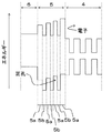
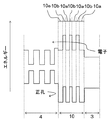
n型窒化ガリウム系半導体層3は、発光層4と接する第2ブロック層10を有していてもよい。第2ブロック層10は、正孔ブロック層10aおよび電子トンネル層10bにより構成されている。ここで図6に、n型窒化ガリウム系半導体3、第2ブロック層10および発光層4のエネルギーバンド図を示す。
(Modification 3 of light emitting element)
The n-type gallium nitride based semiconductor layer 3 may have a second block layer 10 in contact with the light emitting layer 4. The second block layer 10 includes a hole block layer 10a and an electron tunnel layer 10b. Here, FIG. 6 shows an energy band diagram of the n-type gallium nitride based semiconductor 3, the second block layer 10 and the light emitting layer 4.

正孔ブロック層10aは、シリコンを含有するように設けられている。すなわち、正孔ブロック層10aは、シリコンをドープすることによって設けることができ、含有量が、例えば1×10¹⁸/cm以上1×1020/cm以下となるように設けられている。電子トンネル層10bは、正孔ブロック層10aよりもシリコンの含有量が小さくなるように設定されており、含有量が、例えば9.0×1017/cm以下となるように設けられている。このようにn型窒化ガリウム系半導体層3に、正孔ブロック層10aよりもシリコンの含有量が小さい電子トンネル層10bを有する第2ブロック層10を設けることにより、第2ブロック層10の結晶性を向上させることができる。そして、第2ブロック層10の結晶性を向上させることにより、第2ブロック層10上に積層される発光層4およびp型窒化ガリウム系半導体層6の結晶性を向上させることができる。 The hole blocking layer 10a is provided so as to contain silicon. That is, the hole blocking layer 10a can be provided by doping silicon, and is provided so that the content is, for example, 1 × 10 18 / cm 3 or more and 1 × 10 20 / cm 3 or less. The electron tunnel layer 10b is set so that the silicon content is smaller than that of the hole blocking layer 10a, and is provided so that the content is, for example, 9.0 × 10 17 / cm 3 or less. Thus, by providing the n-type gallium nitride based semiconductor layer 3 with the second block layer 10 having the electron tunnel layer 10b having a silicon content smaller than that of the hole block layer 10a, the crystallinity of the second block layer 10 is obtained. Can be improved. Then, by improving the crystallinity of the second block layer 10, the crystallinity of the light emitting layer 4 and the p-type gallium nitride based semiconductor layer 6 stacked on the second block layer 10 can be improved.

さらに、電子トンネル層5bは、厚みが、3nm以下となるように設けられている。そのため、n型窒化ガリウム系半導体層3から移動してきた電子が、伝導帯に形成された障壁をトンネルして発光層4に移動するようになる。その結果、正孔ブロック層10aよりも
シリコンの含有量を小さくした電子トンネル層10bを設けることによって、第2ブロック層10の結晶性を向上させるとともに、電子トンネル層10bが電子の移動を妨げにくい構造となっていることから発光素子1の発光効率の低下を抑制することができる。
Further, the electron tunnel layer 5b is provided so as to have a thickness of 3 nm or less. For this reason, electrons that have moved from the n-type gallium nitride based semiconductor layer 3 tunnel to the barrier formed in the conduction band and move to the light emitting layer 4. As a result, by providing the electron tunneling layer 10b having a silicon content smaller than that of the hole blocking layer 10a, the crystallinity of the second blocking layer 10 is improved and the electron tunneling layer 10b is unlikely to hinder the movement of electrons. Since it has a structure, it is possible to suppress a decrease in light emission efficiency of the light emitting element 1.

<発光素子の製造方法>
次に、本発明の発光素子の製造方法の実施の形態の一例を説明する。図7および図8は、発光素子1の製造方法を説明するための断面図であり、図2に示す発光素子1のA−A’線における断面に相当する部分を示している。本例の発光素子の製造方法は、主に、光半導体層7を順次積層する工程および電極層を形成する工程を有している。以下、各工程について説明する。
<Method for manufacturing light-emitting element>
Next, an example of an embodiment of a method for manufacturing a light emitting element of the present invention will be described. 7 and 8 are cross-sectional views for explaining a method for manufacturing the light-emitting element 1, and show a portion corresponding to a cross section taken along the line AA 'of the light-emitting element 1 shown in FIG. The manufacturing method of the light emitting element of this example mainly includes a step of sequentially laminating the optical semiconductor layer 7 and a step of forming an electrode layer. Hereinafter, each step will be described.

(光半導体層を順次積層する工程)
図7に示すように、基板2上に光半導体層7を形成する。光半導体層7は、n型窒化ガリウム系半導体層3、発光層4、ブロック層5およびp型窒化ガリウム系半導体層6を順次積層した積層構造体で構成する。光半導体層7は、基板2上に例えば有機金属気相成長法によって成長させる。光半導体層7を成長させる他の方法として、例えば分子線エピタキシー法、ハイドライド気相成長法またはパルス・レーザ・デポジション法などを用いることができる。なお、光半導体層7としてはIII−V族半導体を用いることができ、p型またはn型の導電型を半導体に付与する際には、光半導体層7を結晶成長させながら添加物を混ぜればよい。
(Step of sequentially laminating optical semiconductor layers)
As shown in FIG. 7, the optical semiconductor layer 7 is formed on the substrate 2. The optical semiconductor layer 7 is composed of a stacked structure in which an n-type gallium nitride based semiconductor layer 3, a light emitting layer 4, a block layer 5, and a p-type gallium nitride based semiconductor layer 6 are sequentially stacked. The optical semiconductor layer 7 is grown on the substrate 2 by, for example, a metal organic chemical vapor deposition method. As another method for growing the optical semiconductor layer 7, for example, a molecular beam epitaxy method, a hydride vapor phase growth method, a pulse laser deposition method, or the like can be used. Note that a group III-V semiconductor can be used as the optical semiconductor layer 7. When a p-type or n-type conductivity type is imparted to a semiconductor, an additive may be mixed while the optical semiconductor layer 7 is crystal-grown. Good.

ブロック層5は、p型窒化ガリウム系半導体層6においてマグネシウムを含有させる量を変化させればよい。具体的には、電子ブロック層5aを形成する際にマグネシウムを供給するとともに、正孔トンネル層5bを形成する際にマグネシウムの供給を中止することにより、電子ブロック層5aおよび正孔トンネル層5bにおいてマグネシウムの含有量を変化させればよい。   The block layer 5 may change the amount of magnesium contained in the p-type gallium nitride based semiconductor layer 6. Specifically, by supplying magnesium when forming the electron blocking layer 5a and stopping the supply of magnesium when forming the hole tunneling layer 5b, the electron blocking layer 5a and the hole tunneling layer 5b What is necessary is just to change content of magnesium.

(電極層を形成する工程)
このように形成した光半導体層7に電極層を形成する。具体的には、基板2上に光半導体層7を成長させた後、エッチングなどでp型窒化ガリウム系半導体層6、ブロック層5および発光層4の一部を除去することにより、n型窒化ガリウム系半導体層3の上面を露出させる方法を用いることができる。なお、n型窒化ガリウム系半導体層3の上面の一部である露出領域Spは、n型窒化ガリウム系半導体層3の上面の一部だけでなく、n型窒化ガリウム系半導体層3の一部がエッチングで削れることによって露出した表面であってもよい。
(Step of forming the electrode layer)
An electrode layer is formed on the optical semiconductor layer 7 thus formed. Specifically, after growing the optical semiconductor layer 7 on the substrate 2, the p-type gallium nitride based semiconductor layer 6, the block layer 5, and the light emitting layer 4 are partially removed by etching or the like, so that n-type nitridation is performed. A method of exposing the upper surface of the gallium based semiconductor layer 3 can be used. The exposed region Sp that is a part of the upper surface of the n-type gallium nitride semiconductor layer 3 is not only a part of the upper surface of the n-type gallium nitride semiconductor layer 3 but also a part of the n-type gallium nitride semiconductor layer 3. May be a surface exposed by etching.

そして、次に、図8に示すように、n型窒化ガリウム系半導体層3の露出領域Spに発光層4、ブロック層5およびp型窒化ガリウム系半導体層6と間をあけて第1電極層8を形成する。さらに、p型窒化ガリウム系半導体層6上に、第2電極層9を形成する。   Then, as shown in FIG. 8, the first electrode layer is formed with the light emitting layer 4, the block layer 5, and the p-type gallium nitride semiconductor layer 6 in the exposed region Sp of the n-type gallium nitride semiconductor layer 3. 8 is formed. Further, the second electrode layer 9 is formed on the p-type gallium nitride based semiconductor layer 6.

第1電極層8および第2電極層9は、例えば、アルミニウム、チタン、ニッケル、クロム、インジウム、錫、モリブデン、銀、金、タンタルまたは白金などの金属や、それらの金属を含む合金膜や、酸化錫、酸化インジウムまたは酸化インジウム錫などの酸化物などを用いることができる。第1電極層8および第2電極層9を設ける方法としては、例えば金属を用いる場合は、スパッタリング法または蒸着法などを用いることができる。   The first electrode layer 8 and the second electrode layer 9 are, for example, metals such as aluminum, titanium, nickel, chromium, indium, tin, molybdenum, silver, gold, tantalum or platinum, alloy films containing these metals, An oxide such as tin oxide, indium oxide, or indium tin oxide can be used. As a method of providing the first electrode layer 8 and the second electrode layer 9, for example, when using a metal, a sputtering method or a vapor deposition method can be used.

1 発光素子
2 基板
3 n型窒化ガリウム系半導体層
4 発光層
5 ブロック層
5a 電子ブロック層
5b 正孔トンネル層
6 p型窒化ガリウム系半導体層
7 光半導体層
8 第1電極層
9 第2電極層
10 第2ブロック層
10a 正孔ブロック層
10b 電子トンネル層
DESCRIPTION OF SYMBOLS 1 Light emitting element 2 Substrate 3 N type gallium nitride semiconductor layer 4 Light emitting layer 5 Block layer 5a Electron block layer 5b Hole tunnel layer 6 P type gallium nitride semiconductor layer 7 Photo semiconductor layer 8 First electrode layer 9 Second electrode layer
10 Second block layer
10a Hole blocking layer
10b electron tunnel layer

Claims (4)

n型窒化ガリウム系半導体層と、
該n型窒化ガリウム系半導体層上に設けられた、窒化ガリウム系半導体を含む発光層と、該発光層上に設けられた、該発光層と接するブロック層を持つp型窒化ガリウム系半導体層とを有し、
前記ブロック層は、マグネシウムを含有した電子ブロック層と、該電子ブロック層よりもマグネシウムの含有量が小さい、厚みが3nm以下の正孔トンネル層とが積層された発光素子。
an n-type gallium nitride based semiconductor layer;
A light-emitting layer including a gallium nitride-based semiconductor provided on the n-type gallium nitride-based semiconductor layer, and a p-type gallium nitride-based semiconductor layer provided on the light-emitting layer and having a block layer in contact with the light-emitting layer; Have
The block layer is a light emitting element in which an electron block layer containing magnesium and a hole tunnel layer having a magnesium content smaller than the electron block layer and a thickness of 3 nm or less are stacked.
前記電子ブロック層は、前記発光層から遠ざかるにつれてマグネシウムの含有量が次第に小さくなっている請求項1に記載の発光素子。   The light-emitting element according to claim 1, wherein the electron blocking layer has a magnesium content that gradually decreases as the distance from the light-emitting layer increases. 前記正孔トンネル層は、マグネシウムを含有していない請求項1に記載の発光素子。   The light emitting device according to claim 1, wherein the hole tunnel layer does not contain magnesium. 前記n型窒化ガリウム系半導体層は、前記発光層と接する第2ブロック層を持ち、該第2ブロック層は、シリコンを含有した正孔ブロック層と、該正孔ブロック層よりもシリコンの含有量が小さい、厚みが3nm以下の電子トンネル層とが積層された請求項1−3のいずれかに記載の発光素子。   The n-type gallium nitride based semiconductor layer has a second block layer in contact with the light emitting layer, and the second block layer has a hole blocking layer containing silicon and a silicon content more than the hole blocking layer. The light emitting element in any one of Claims 1-3 with which the electron tunnel layer whose thickness is 3 nm or less is laminated | stacked.
JP2011075192A 2011-03-30 2011-03-30 Light-emitting device Withdrawn JP2012209488A (en)

Priority Applications (1)

Application Number Priority Date Filing Date Title
JP2011075192A JP2012209488A (en) 2011-03-30 2011-03-30 Light-emitting device

Applications Claiming Priority (1)

Application Number Priority Date Filing Date Title
JP2011075192A JP2012209488A (en) 2011-03-30 2011-03-30 Light-emitting device

Publications (1)

Publication Number Publication Date
JP2012209488A true JP2012209488A (en) 2012-10-25

Family

ID=47188970

Family Applications (1)

Application Number Title Priority Date Filing Date
JP2011075192A Withdrawn JP2012209488A (en) 2011-03-30 2011-03-30 Light-emitting device

Country Status (1)

Country Link
JP (1) JP2012209488A (en)

Cited By (2)

* Cited by examiner, † Cited by third party
Publication number Priority date Publication date Assignee Title
US9312439B2 (en) 2014-01-09 2016-04-12 Samsung Electronics Co., Ltd. Semiconductor light emitting device
JP2021174813A (en) * 2020-04-21 2021-11-01 日亜化学工業株式会社 Method of manufacturing light-emitting element

Cited By (4)

* Cited by examiner, † Cited by third party
Publication number Priority date Publication date Assignee Title
US9312439B2 (en) 2014-01-09 2016-04-12 Samsung Electronics Co., Ltd. Semiconductor light emitting device
US9941443B2 (en) 2014-01-09 2018-04-10 Samsung Electronics Co., Ltd. Semiconductor light emitting device
JP2021174813A (en) * 2020-04-21 2021-11-01 日亜化学工業株式会社 Method of manufacturing light-emitting element
JP7149486B2 (en) 2020-04-21 2022-10-07 日亜化学工業株式会社 Method for manufacturing light-emitting element

Similar Documents

Publication Publication Date Title
JP4994758B2 (en) Gallium nitride semiconductor light emitting device and method for manufacturing the same
CN103229316B (en) Light-emitting device and manufacture method thereof
JP5162016B1 (en) Semiconductor device, wafer, semiconductor device manufacturing method, and wafer manufacturing method
US8148180B2 (en) Techniques of forming Ohmic contacts on GaN light emitting diodes
US20120273753A1 (en) Semiconductor light emitting device
JPWO2012127660A1 (en) Nitride semiconductor ultraviolet light emitting device
TWI680590B (en) Nitride semiconductor light emitting element and method for manufacturing nitride semiconductor light emitting element
JP5713856B2 (en) Light transmissive metal electrode, electronic device and optical element
JP6155478B2 (en) Photoactive device with improved charge carrier distribution and method for forming the same
CN111373552B (en) Nitride semiconductor light-emitting element
JP2005244201A (en) Semiconductor luminous element and manufacturing method of the same
US20130099198A1 (en) Semiconductor light emitting element and method of manufacturing the same
JP2011040739A (en) Vertical light emitting diode and manufacturing method of the same
JP2016513879A (en) Semiconductor light-emitting structure having an active region containing InGaN and method of manufacturing the same
KR101263286B1 (en) Semiconductor optoelectronic device and method for manufacturing thereof
US20120241803A1 (en) Semiconductor light emitting device and method for manufacturing same
CN107833956B (en) Nitride semiconductor structure and semiconductor light emitting element
JP2012209488A (en) Light-emitting device
KR20150042409A (en) A method of manufacturing a light emitting device
JP2008071910A (en) Nitride semiconductor light emitting diode element and its manufacturing method
JP2008141047A (en) Nitride semiconductor light emitting element
JP2008053385A (en) Nitride semiconductor light emitting diode element
KR100830643B1 (en) Method of manufacturing light emitting device
JPWO2022038769A5 (en)
JPWO2022009306A5 (en)

Legal Events

Date Code Title Description
A300 Withdrawal of application because of no request for examination

Free format text: JAPANESE INTERMEDIATE CODE: A300

Effective date: 20140603