JP2012204723A - Charged particle beam drawing method and manufacturing method of article using the same - Google Patents
Charged particle beam drawing method and manufacturing method of article using the same Download PDFInfo
- Publication number
- JP2012204723A JP2012204723A JP2011069409A JP2011069409A JP2012204723A JP 2012204723 A JP2012204723 A JP 2012204723A JP 2011069409 A JP2011069409 A JP 2011069409A JP 2011069409 A JP2011069409 A JP 2011069409A JP 2012204723 A JP2012204723 A JP 2012204723A
- Authority
- JP
- Japan
- Prior art keywords
- region
- charged particle
- particle beam
- self
- calibration
- Prior art date
- Legal status (The legal status is an assumption and is not a legal conclusion. Google has not performed a legal analysis and makes no representation as to the accuracy of the status listed.)
- Granted
Links
Images


Landscapes
- Electron Beam Exposure (AREA)
Abstract
Description
本発明は、荷電粒子線描画方法、およびそれを用いた物品の製造方法に関する。 The present invention relates to a charged particle beam drawing method and an article manufacturing method using the same.
従来、半導体デバイスなどの製造工程におけるリソグラフィー工程では、種々のリソグラフィー装置が用いられている。このリソグラフィー装置としては、例えば、ArF、i−ArF、EUVなどによる露光装置、ML2などの荷電粒子線描画装置、またはインプリント装置などが挙げられる。このようなリソグラフィー装置では、荷電粒子線描画装置を除き、パターン付きの原版として、マスク、レチクル、またはモールド(テンプレートやスタンパー)などが採用されている。通常、この原版にパターンを形成する装置としては、荷電粒子線描画装置を用いることが多い。一般に、荷電粒子線描画装置は、荷電粒子線である電子ビームを発生する電子銃と、原版を載置して適宜移動させる移動ステージとを有する。この場合、移動ステージの位置は、別途設置された干渉計で計測され、移動ステージの位置に対して、電子ビームの照射位置を偏向器にて所定の位置に決めながら原版上に所望のパターンを描画する。 Conventionally, various lithography apparatuses are used in a lithography process in a manufacturing process of a semiconductor device or the like. Examples of the lithography apparatus include an exposure apparatus using ArF, i-ArF, EUV, and the like, a charged particle beam drawing apparatus such as ML2, or an imprint apparatus. In such a lithography apparatus, except for a charged particle beam drawing apparatus, a mask, a reticle, a mold (template or stamper), or the like is employed as an original plate with a pattern. Usually, a charged particle beam drawing apparatus is often used as an apparatus for forming a pattern on the original. In general, a charged particle beam drawing apparatus includes an electron gun that generates an electron beam that is a charged particle beam, and a moving stage on which an original plate is placed and moved appropriately. In this case, the position of the moving stage is measured by an interferometer installed separately, and a desired pattern is formed on the original plate while determining the irradiation position of the electron beam to a predetermined position with a deflector with respect to the position of the moving stage. draw.
この位置決めの方法として、近年、ある描画領域(転写領域)にて重ね合わせ精度(例えば、ずれの許容度)を低くして自動でアライメントを行うことで、全体の位置決め時間を短縮させるセルフアライメントと呼ばれる技術が採用されている。例えば、特許文献1は、原版ではなく半導体デバイス(基板)のアライメントに関するものではあるが、セルフアライメントによるクロスポイントタイプのメモリー製造について開示している。
As this positioning method, in recent years, self-alignment that shortens the overall positioning time by automatically performing alignment with a low overlay accuracy (for example, tolerance of deviation) in a certain drawing area (transfer area) The so-called technology is adopted. For example,
しかしながら、特許文献1では、特に、原版に対してパターンを描画する場合の全体の位置決め時間を短縮させるような技術が提案されていない。
However,
本発明は、このような状況を鑑みてなされたものであり、例えば、セルフアライメントを採用する上で好適となる荷電粒子線描画方法を提供することを目的とする。 The present invention has been made in view of such a situation, and an object of the present invention is to provide a charged particle beam drawing method suitable for adopting, for example, self-alignment.
上記課題を解決するために、本発明は、荷電粒子線を用いて被処理体にパターンを描画する荷電粒子線描画方法であって、被処理体の描画領域として第1領域と第2領域とを設定する工程と、第1領域の描画を行うとともに、該第1領域の描画の開始から終了までの間に荷電粒子線の位置ずれ量を補正するための第1キャリブレーションを行う工程と、第2領域の描画を行うとともに、該第2領域の描画の開始から終了までの間に荷電粒子線の位置ずれ量を補正するための第2キャリブレーションを行う工程と、を有し、第1キャリブレーションと第2キャリブレーションとを行う頻度が異なることを特徴とする。 In order to solve the above problems, the present invention is a charged particle beam drawing method for drawing a pattern on a target object using a charged particle beam, wherein a first area and a second area are drawn as a drawing area of the target object. And a step of performing a first calibration for correcting a positional deviation amount of the charged particle beam between the start and the end of the drawing of the first region, Performing a second area drawing and performing a second calibration for correcting a positional deviation amount of the charged particle beam from the start to the end of the drawing of the second area. The frequency of performing the calibration and the second calibration is different.
本発明によれば、例えば、セルフアライメントを採用する上で好適となる荷電粒子線描画方法を提供することができる。 According to the present invention, for example, a charged particle beam drawing method suitable for adopting self-alignment can be provided.
以下、本発明を実施するための形態について図面等を参照して説明する。 Hereinafter, embodiments for carrying out the present invention will be described with reference to the drawings.
まず、本発明の一実施形態に係る荷電粒子線描画装置(以下、単に「描画装置」と表記する)について説明する。以下、各実施形態において説明する描画装置は、単数の電子ビーム(荷電粒子線)の照射により、所定の描画データを被処理体である原版の所定の位置に描画するものである。なお、荷電粒子線は、本実施形態のような電子線に限定されず、イオン線などの他の荷電粒子線であってもよい。また、本実施形態における原版は、特にリソグラフィー装置である露光装置に採用されるマスクやレチクル、またはインプリント装置に採用されるモールドなどを想定しているが、製造物である半導体デバイスなどに使用される基板に対する描画にも適用可能である。 First, a charged particle beam drawing apparatus (hereinafter simply referred to as “drawing apparatus”) according to an embodiment of the present invention will be described. Hereinafter, the drawing apparatus described in each embodiment draws predetermined drawing data at a predetermined position of an original plate, which is an object to be processed, by irradiation with a single electron beam (charged particle beam). The charged particle beam is not limited to the electron beam as in the present embodiment, and may be another charged particle beam such as an ion beam. In addition, the original plate in the present embodiment is assumed to be a mask or reticle employed in an exposure apparatus that is a lithography apparatus, or a mold employed in an imprint apparatus, but is used for a semiconductor device that is a product. The present invention is also applicable to drawing on a substrate to be performed.
図1は、本実施形態に係る描画装置の構成を示す図である。なお、以下の各図では、原版に対する電子ビームの照射方向にZ軸を取り、Z軸に垂直な平面内に互いに直交するX軸およびY軸を取っている。さらに、以下の各図では、図1と同一構成のものには同一の符号を付す。この描画装置1は、電子銃2と、該電子銃2から照射された電子ビーム(電子線)3を偏向および結像させる光学系4と、原版5を保持するステージ6と、描画装置1の各構成要素の動作などを制御する制御部7とを備える。なお、電子ビームは、大気圧雰囲気ではすぐに減衰し、また高電圧による放電を防止する意味もかねて、制御部7を除く上記構成要素は、不図示の真空排気系により内部圧力が適宜調整された空間内に設置される。例えば、電子銃2および光学系4は、高い真空度に保たれた電子光学鏡筒8内に設置される。同様に、ステージ6は、電子光学鏡筒8内よりも比較的低い真空度に保たれた描画室9内に設置される。
FIG. 1 is a diagram illustrating a configuration of a drawing apparatus according to the present embodiment. In each of the following drawings, the Z axis is taken in the electron beam irradiation direction with respect to the original, and the X axis and Y axis perpendicular to each other are taken in a plane perpendicular to the Z axis. Further, in the following drawings, the same components as those in FIG. The
電子銃2は、熱や電界の印加により電子ビーム3を放出する機構である。光学系4は、不図示であるが、各種偏向器およびレンズを有する。偏向器としては、例えば、電子ビームの照射のON/OFF動作を実施するもの(ブランキング偏向器)や、ステージ6上に載置された原版5の表面上の像をXY方向に偏向するものなどがある。また、レンズとしては、コリメータレンズ、または、電子ビーム3のクロスオーバを形成したり、電子ビーム3を原版5の描画領域に結像させたりする静電レンズなどがある。ステージ6は、例えば静電吸着により原版5を保持しつつ、XY平面内を電子ビーム3の照射位置に対して適宜移動可能とする保持部である。また、ステージ6は、その側端部に反射ミラー10を備え、一方、描画室9は、反射ミラー10の設置位置に対向して、その内壁面に位置計測装置である干渉計(レーザー測長器)11を備える。ステージ6の位置は、この干渉計11により実時間で計測される。なお、本実施形態では、位置計測装置として干渉計11を採用するが、この位置計測装置の種類は、特に限定するものではない。さらに、ステージ6は、電子ビーム3の位置を検出する電子ビーム検出器12を備える。この電子ビーム検出器12は、不図示であるが、検出素子(位置センサ)と該検出素子の検出面の一部を覆うナイフエッジとからなり、検出面に入射する電子ビーム3の強度(電流値)を制御部7に対して出力する。なお、電子ビーム検出器12は、本実施形態ではステージ6に設置する構成としているが、例えば、電子ビーム3の経路上の1箇所以上に挿入可能に構成されていてもよい。または、電子ビーム検出器12は、ステージ6上に限られず、別途専用のステージに設置されてもよい。さらに、ナイフエッジの設置も必須ではなく、電子ビーム3の入射量を適宜調節可能であれば、その構成は問わない。
The
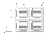
次に、本実施形態に適用される原版5の構成について説明する。図2は、原版5の描画領域(4チップ分の1ショット)の内部配置を示す概略図である。原版5は、例えば石英ガラスからなる被処理体であり、描画領域上には感光性のレジストが塗布されている。特に、原版5上の1チップ分の領域Aは、図2に示すようにパターンが描画される2種類のパターン群P1、P2で構成されている。このうち、第1パターン群P1は、30nm以下の微細な線幅で構成され、ここでの重ね合わせ精度、すなわち、電子ビーム3の入射位置と所望の描画位置とのずれの許容度は、線幅よりも大きくてもよい領域である。次に、第2パターン群P2は、第1パターン群P1の線幅よりも数倍大きな線幅で構成され、ここでの重ね合わせ精度は、線幅の1/3以下とする領域である。さらに、領域Aの外周部には、スクライブ領域Bが配置され、このスクライブ領域Bは、重ね合わせ検査用のマークや次の製造工程で使用するためのアライメントマークが形成される領域となる。なお、このスクライブ領域Bに形成されるマークには、CD検査用のマークなど厳しい位置精度が要求されないものも含む。
Next, the configuration of the original 5 applied to this embodiment will be described. FIG. 2 is a schematic diagram showing the internal arrangement of the drawing area (one shot for four chips) of the original 5. The original 5 is an object to be processed made of, for example, quartz glass, and a photosensitive resist is applied on the drawing area. Particularly, the area A for one chip on the original 5 is composed of two types of pattern groups P1 and P2 on which patterns are drawn as shown in FIG. Among these, the first pattern group P1 is configured with a fine line width of 30 nm or less, and the overlay accuracy here, that is, the tolerance of the deviation between the incident position of the
まず、第1パターン群P1は、本実施形態のセルフアライメントが適用される第1領域である。セルフアライメントは、例えば半導体デバイスの形成工程において、予め部分的に厚さの異なる膜を形成し、転写処理を行わずに全面をエッチングすることで、一部に穴を開けてベース領域とエミッタ領域と呼ばれるパターンを形成する際に適用されるものである。セルフアライメントは、この方法だけに限定するものでなく、前述のクロスポイントタイプのメモリーデバイスにも適用されている。これらのセルフアライメントを適用したデバイスにおいては、アライメントに要求される精度が低くなる。すなわち、近年のデバイス回路(半導体デバイス)では、最も細いパターンに対してその線幅の1/3以下の値となる重ね合わせ精度が既存のデザインルールとして要求されるが、この領域に関しては、要求精度は、既存のデザインルールよりも低い精度で良くなる。 First, the first pattern group P1 is a first region to which the self-alignment of this embodiment is applied. In the self-alignment process, for example, in the process of forming a semiconductor device, a film having a partially different thickness is formed in advance, and the entire surface is etched without performing a transfer process. This is applied when forming a pattern called. Self-alignment is not limited to this method, but is also applied to the above-mentioned cross-point type memory device. In devices to which these self-alignments are applied, the accuracy required for alignment is low. That is, in recent device circuits (semiconductor devices), an overlay design accuracy that is 1/3 or less of the line width of the thinnest pattern is required as an existing design rule. The accuracy is better with lower accuracy than existing design rules.
次に、第2パターン群P2は、要求される重ね合わせ精度が高いため、本実施形態のセルフアライメントが適用されない領域(非セルフアライメント領域:第2領域)である。例えば、この第2パターン群P2は、メモリーデバイスにおける呼び出しまたは読み込みのための周辺回路を形成するための領域となる。ここで、セルフアライメントを適用するデバイス回路においては、その重ね合わせ精度は、他の領域と比較して微細な線幅を有する第1パターン群P1で決定せずに、それほど微細でない線幅を有する第2パターン群P2に関して決定される。例えば、第2パターン群P2の線幅は、現状のデザインルールでみると、上述のとおり第1パターン群P1の最も微細な線幅の数倍である。具体的には、第1パターン群P1では、ハーフピッチ30nmで重ね合わせ精度が30nmとすると、第2パターン群P2では、ハーフピッチ60nmで重ね合わせ精度が20nmである。この第2パターン群P2を原版5上に形成するときには、描画装置1のアドレスを最小とする必要がなく、また、第1パターン群P1と比較すると、描画面積が1/5程度と少ないため、ここでの描画時間は、数十分程度である。一方、重ね合わせ検査用のマークなどが形成されるスクライブ領域Bも、非セルフアライメント領域(第2領域)である。このスクライブ領域Bにおいても、要求される重ね合わせ精度は、第2パターン群P2と同様の精度でよく、ここでの描画時間は、数分程度となる。したがって、セルフアライメントを適用する原版5では、第2パターン群P2およびスクライブ領域Bを描画する数十分程度の時間内で、最も重ね合わせ精度を出す必要がある。
Next, the second pattern group P2 is a region to which the self-alignment of this embodiment is not applied (non-self-alignment region: second region) because the required overlay accuracy is high. For example, the second pattern group P2 is an area for forming a peripheral circuit for calling or reading in the memory device. Here, in the device circuit to which self-alignment is applied, the overlay accuracy is not determined by the first pattern group P1 having a fine line width compared to other regions, and has a line width that is not so fine. The second pattern group P2 is determined. For example, the line width of the second pattern group P2 is several times the finest line width of the first pattern group P1, as described above, according to the current design rules. Specifically, in the first pattern group P1, when the overlay accuracy is 30 nm and the overlay accuracy is 30 nm, in the second pattern group P2, the overlay accuracy is 20 nm and the half pitch is 60 nm. When the second pattern group P2 is formed on the
次に、描画装置1による描画方法について説明する。図3は、本実施形態に係る描画処理の流れを示すフローチャートである。まず、制御部7は、描画処理を開始すると、非セルフアライメント領域である第2パターン群P2およびスクライブ領域Bに対する描画を実施させる(ステップS100)。次に、制御部7は、このステップS100の描画において、あるインターバル時間(第1時間)T1が経過したら(ステップS101)、一旦描画を中止させる(ステップS102)。ここで、電子ビーム3は、インターバル時間T1の間に、周囲の熱や磁場の影響などに起因し、基準位置に対してずれが生じる。そこで、このインターバル時間T1は、そのずれ量が、必要とされる重ね合わせ精度よりも小さくなるように予め設定される。次に、制御部7は、電子ビーム3の第1キャリブレーション(位置の補正)を実施させる(ステップS103)。この場合、制御部7は、まずステージ6を走査させて、該ステージ6上に設置された電子ビーム検出器12を電子ビーム3の照射位置に向けて移動させ、このとき検出素子が検出した出力と、干渉計11の計測値との関係を取得する。そして、制御部7は、この検出素子の出力が所定の値となるステージ6の位置において、干渉計11の計測値がゼロになるように干渉計11の計測値を補正し、第1キャリブレーションを終了する。次に、制御部7は、この第1キャリブレーションが終了した後、ステップS100の描画を再開し、再度、ステップS101以下の工程を実行する。そして、制御部7は、このステップS100からステップS103までの一連の工程を所定の回数で繰り返した後、4チップ領域分の非セルフアライメント領域の描画処理を終了する。
Next, a drawing method by the
上記非セルフアライメント領域に対する描画処理が終了した後、次に、制御部7は、セルフアライメント領域である第1パターン群P1に対する描画を実施させる(ステップS104)。次に、制御部7は、このステップS104の描画において、あるインターバル時間(第2時間)T2が経過したら(ステップS105)、一旦描画を中止させる(ステップS106)。このインターバル時間T2の間においても、インターバル時間T1の間と同様に電子ビーム3のずれが生じる。したがって、上記と同様に、インターバル時間T2は、そのずれ量が、必要とされる重ね合わせ精度よりも小さくなるように予め設定される。ここで、インターバル時間T2は、インターバル時間T1よりも長いので、インターバル時間T2の間に生ずる電子ビーム3のずれ量は、インターバル時間T1の間に生じるずれ量よりも大きくなる。しかしながら、このセルフアライメント領域では、非セルフアライメント領域よりも要求される重ね合わせ精度が低いので、ずれ量が大きくなったとしても許容され得る。次に、制御部7は、ステップS103と同様の電子ビーム3の第2キャリブレーションを実施させる(ステップS107)。なお、第1パターン群P1のようなセルフアライメント領域では、描画装置1の動作が安定している場合には、制御部7は、第2キャリブレーションを実施させなくてもよい場合もある。次に、制御部7は、この第2キャリブレーションが終了した後、ステップS104の描画を再開し、再度、ステップS104以下の工程を実行する。そして、制御部7は、このステップS104からステップS107までの一連の工程を所定の回数で繰り返した後、4チップ領域分のセルフアライメント領域の描画処理を終了し、4チップ領域全体の描画処理が終了する。なお、この図3に示すフローチャートの流れでは、一例として非セルフアライメント領域に対する描画を先に実施し、その後セルフアライメント領域に対する描画を実施するものとしたが、逆の順番でもよい。
After the drawing process for the non-self-alignment region is completed, the control unit 7 then performs drawing for the first pattern group P1 that is the self-alignment region (step S104). Next, when a certain interval time (second time) T2 has elapsed in the drawing in step S104 (step S105), the control unit 7 temporarily stops the drawing (step S106). Even during the interval time T2, the
上記のように、セルフアライメント領域を描画中のインターバル時間T2は、非セルフアライメント領域を描画中のインターバル時間T1よりも長い。したがって、キャリブレーションの頻度は、非セルフアライメント領域を描画中のときよりも、セルフアライメント領域を描画中のときの方が少ない。すなわち、本実施形態の総キャリブレーション頻度は、描画領域の全てを非セルフアライメント領域とする従来の描画におけるキャリブレーション頻度と比較すると少なくなる。これにより、描画装置1は、総キャリブレーション時間を短くすることができるので、位置決め時間を短縮させることで原版5全体への描画時間も短くすることができ、結果的に、生産性を向上させることが可能となる。一般に、原版に対して描画を実施するには、その描画装置の最小アドレスで、1枚の原版に対して数十時間以上を要する。したがって、本実施形態のように、総キャリブレーション時間を短くできることの効果は、非常に大きい。
As described above, the interval time T2 during drawing of the self-alignment region is longer than the interval time T1 during drawing of the non-self-alignment region. Therefore, the frequency of calibration is lower when the self-alignment region is being drawn than when the non-self-alignment region is being drawn. That is, the total calibration frequency of the present embodiment is less than the calibration frequency in the conventional drawing in which all of the drawing area is a non-self-alignment area. Thereby, since the
以上のように、本実施形態によれば、位置決め時間の短縮により生産性を向上させることができるなど、セルフアライメントを採用する上で好適となる描画方法を提供することができる。 As described above, according to this embodiment, it is possible to provide a drawing method that is suitable for adopting self-alignment, for example, productivity can be improved by shortening the positioning time.
なお、上記実施形態に示した描画方法に加え、ステージ6の熱変形も考慮し得る。図4は、描画経過時間に対するステージ6の熱変形を示すグラフである。図4に示すように、ステージ6の熱変形は、描画経過時間に対して1次遅れの形で表現される。ここで、描画が開始された初期の過渡状態では、ステージ6の熱変形の変化量が大きく、以後、時間の経過に伴い変化量が小さくなる。通常、熱変形の変化量が大きい時間帯では、電子ビーム3のずれ量も大きくなるため、特にこの時間帯に、重ね合わせ精度の低いセルフアライメント領域の描画を行うことが望ましい。このセルフアライメント領域に対する描画が終了した後、重ね合わせ精度の高い非セルフアライメント領域の描画を行う。これにより、さらにキャリブレーションの頻度を少なくすることができる。
In addition to the drawing method shown in the above embodiment, thermal deformation of the
(物品の製造方法)
本発明の実施形態に係る物品の製造方法は、例えば、半導体デバイスなどのマイクロデバイスや微細構造を有する素子などの物品を製造するのに好適である。該製造方法は、感光剤が塗布された基板(原版)の該感光剤に上記の描画装置を用いて潜像パターンを形成する工程(基板に描画を行う工程)と、該工程で潜像パターンが形成された基板を現像する工程とを含み得る。さらに、該製造方法は、他の周知の工程(酸化、成膜、蒸着、ドーピング、平坦化、エッチング、レジスト剥離、ダイシング、ボンディング、パッケージングなど)を含み得る。本実施形態の物品の製造方法は、従来の方法に比べて、物品の性能・品質・生産性・生産コストの少なくとも1つにおいて有利である。
(Product manufacturing method)
The method for manufacturing an article according to an embodiment of the present invention is suitable for manufacturing an article such as a micro device such as a semiconductor device or an element having a fine structure. The manufacturing method includes a step of forming a latent image pattern on the photosensitive agent of the substrate (original plate) coated with the photosensitive agent using the above drawing device (step of drawing on the substrate), and the latent image pattern in the step. Developing the substrate on which is formed. Further, the manufacturing method may include other well-known steps (oxidation, film formation, vapor deposition, doping, planarization, etching, resist stripping, dicing, bonding, packaging, and the like). The method for manufacturing an article according to the present embodiment is advantageous in at least one of the performance, quality, productivity, and production cost of the article as compared with the conventional method.
以上、本発明の好ましい実施形態について説明したが、本発明は、これらの実施形態に限定されず、その要旨の範囲内で種々の変形および変更が可能である。 As mentioned above, although preferable embodiment of this invention was described, this invention is not limited to these embodiment, A various deformation | transformation and change are possible within the range of the summary.
1 荷電粒子線描画装置
3 電子ビーム
5 原版
6 ステージ
A 領域
B スクライブ領域
P1 第1パターン群
P2 第2パターン群
DESCRIPTION OF
Claims (5)
前記被処理体の描画領域として第1領域と第2領域とを設定する工程と、
前記第1領域の描画を行うとともに、該第1領域の描画の開始から終了までの間に前記荷電粒子線の位置ずれ量を補正するための第1キャリブレーションを行う工程と、
前記第2領域の描画を行うとともに、該第2領域の描画の開始から終了までの間に前記荷電粒子線の位置ずれ量を補正するための第2キャリブレーションを行う工程と、
を有し、
前記第1キャリブレーションと前記第2キャリブレーションとを行う頻度が異なることを特徴とする荷電粒子線描画方法。 A charged particle beam drawing method for drawing a pattern on a workpiece using a charged particle beam,
Setting a first region and a second region as a drawing region of the object to be processed;
Performing the first calibration for correcting the positional deviation amount of the charged particle beam between the start and the end of the drawing of the first region, while performing the drawing of the first region;
Performing a second calibration for correcting the positional deviation amount of the charged particle beam between the start and the end of the drawing of the second region, while performing the drawing of the second region;
Have
A charged particle beam drawing method, wherein the frequency of performing the first calibration and the second calibration is different.
前記第1領域、または前記第2領域のいずれか一方の領域では、該領域に形成されるパターンの線幅に対して要求される前記重ね合わせ精度が低く、一方、
他の領域では、該領域に形成されるパターンの線幅に対して要求される前記重ね合わせ精度が高いことを特徴とする請求項1に記載の荷電粒子線描画方法。 The first region and the second region have different overlay accuracy between the incident position of the charged particle beam and the drawing position on the surface of the object to be processed,
In any one of the first region and the second region, the overlay accuracy required for the line width of the pattern formed in the region is low,
2. The charged particle beam drawing method according to claim 1, wherein in another region, the overlay accuracy required for a line width of a pattern formed in the region is high.
前記工程で描画を行われた被処理体を現像する工程と、
を含むことを特徴とする物品の製造方法。 A step of performing drawing on the object to be processed using the charged particle beam drawing apparatus according to claim 1;
Developing the object to be processed in which the drawing is performed in the step;
A method for producing an article comprising:
Priority Applications (1)
| Application Number | Priority Date | Filing Date | Title |
|---|---|---|---|
| JP2011069409A JP5812642B2 (en) | 2011-03-28 | 2011-03-28 | Charged particle beam drawing method and article manufacturing method using the same |
Applications Claiming Priority (1)
| Application Number | Priority Date | Filing Date | Title |
|---|---|---|---|
| JP2011069409A JP5812642B2 (en) | 2011-03-28 | 2011-03-28 | Charged particle beam drawing method and article manufacturing method using the same |
Publications (3)
| Publication Number | Publication Date |
|---|---|
| JP2012204723A true JP2012204723A (en) | 2012-10-22 |
| JP2012204723A5 JP2012204723A5 (en) | 2014-05-01 |
| JP5812642B2 JP5812642B2 (en) | 2015-11-17 |
Family
ID=47185326
Family Applications (1)
| Application Number | Title | Priority Date | Filing Date |
|---|---|---|---|
| JP2011069409A Expired - Fee Related JP5812642B2 (en) | 2011-03-28 | 2011-03-28 | Charged particle beam drawing method and article manufacturing method using the same |
Country Status (1)
| Country | Link |
|---|---|
| JP (1) | JP5812642B2 (en) |
Citations (7)
| Publication number | Priority date | Publication date | Assignee | Title |
|---|---|---|---|---|
| JPS5555533A (en) * | 1978-10-18 | 1980-04-23 | Chiyou Lsi Gijutsu Kenkyu Kumiai | Method of manufacturing semiconductor device |
| JPH09260247A (en) * | 1996-03-22 | 1997-10-03 | Hitachi Ltd | Pattern transfer method and forming method of data for pattern transfer |
| JPH10294260A (en) * | 1997-04-18 | 1998-11-04 | Nec Corp | Pattern exposure system, pattern exposure method and recording medium recording pattern exposure processing program |
| JPH118171A (en) * | 1997-06-16 | 1999-01-12 | Hitachi Ltd | Beam drift correction method of electron beam exposure system and manufacture of semiconductor integrated circuit device using the method |
| JP2001318455A (en) * | 2000-05-12 | 2001-11-16 | Hitachi Ltd | Method for manufacturing semiconductor integrated circuit device |
| JP2005129688A (en) * | 2003-10-23 | 2005-05-19 | Hitachi Ltd | Method of manufacturing semiconductor device |
| JP2007043083A (en) * | 2005-07-04 | 2007-02-15 | Nuflare Technology Inc | Method for correcting beam drift of electron beam, and method for drawing electron beam |
-
2011
- 2011-03-28 JP JP2011069409A patent/JP5812642B2/en not_active Expired - Fee Related
Patent Citations (7)
| Publication number | Priority date | Publication date | Assignee | Title |
|---|---|---|---|---|
| JPS5555533A (en) * | 1978-10-18 | 1980-04-23 | Chiyou Lsi Gijutsu Kenkyu Kumiai | Method of manufacturing semiconductor device |
| JPH09260247A (en) * | 1996-03-22 | 1997-10-03 | Hitachi Ltd | Pattern transfer method and forming method of data for pattern transfer |
| JPH10294260A (en) * | 1997-04-18 | 1998-11-04 | Nec Corp | Pattern exposure system, pattern exposure method and recording medium recording pattern exposure processing program |
| JPH118171A (en) * | 1997-06-16 | 1999-01-12 | Hitachi Ltd | Beam drift correction method of electron beam exposure system and manufacture of semiconductor integrated circuit device using the method |
| JP2001318455A (en) * | 2000-05-12 | 2001-11-16 | Hitachi Ltd | Method for manufacturing semiconductor integrated circuit device |
| JP2005129688A (en) * | 2003-10-23 | 2005-05-19 | Hitachi Ltd | Method of manufacturing semiconductor device |
| JP2007043083A (en) * | 2005-07-04 | 2007-02-15 | Nuflare Technology Inc | Method for correcting beam drift of electron beam, and method for drawing electron beam |
Also Published As
| Publication number | Publication date |
|---|---|
| JP5812642B2 (en) | 2015-11-17 |
Similar Documents
| Publication | Publication Date | Title |
|---|---|---|
| JP4213907B2 (en) | Method and system for improving focus accuracy of a lithography system | |
| KR101988084B1 (en) | Exposure apparatus, and method of manufacturing device | |
| US7202488B2 (en) | Correction system, method of correcting deflection distortion, program and method for manufacturing a semiconductor device | |
| JP2012104853A (en) | Lithographic apparatus and device manufacturing method with double exposure overlay control | |
| JP5068844B2 (en) | Lithographic method and lithographic apparatus | |
| JP2014120746A (en) | Drawing device and method of manufacturing article | |
| US20140209818A1 (en) | Lithography apparatus, lithography method, and method of manufacturing article | |
| JP2016001708A (en) | Lithographic apparatus and method of manufacturing article | |
| EP3396457A1 (en) | Device manufacturing method | |
| JP6251648B2 (en) | Charged particle beam drawing apparatus and charged particle beam drawing method | |
| JP5812642B2 (en) | Charged particle beam drawing method and article manufacturing method using the same | |
| JP2010074043A (en) | Semiconductor manufacturing method and semiconductor manufacturing device | |
| US6559927B1 (en) | Gap adjusting method in exposure apparatus | |
| US9606460B2 (en) | Lithography apparatus, and method of manufacturing article | |
| CN111771167B (en) | Alignment mark positioning in lithographic processes | |
| JP2009177126A (en) | Mask blanks, mask, mask holding apparatus, exposure apparatus and method for manufacturing device | |
| JP2005116849A (en) | Electrostatic adsorption device and method therefor, exposure device, and device manufacturing method | |
| CN111413850B (en) | Exposure apparatus, method for controlling exposure apparatus, and method for manufacturing article | |
| US11709434B2 (en) | Device manufacturing method | |
| JP2007329267A (en) | Device and method for charged-particle-beam lithography | |
| JP4677180B2 (en) | Semiconductor manufacturing apparatus and device manufacturing method | |
| JP2005063993A (en) | Method for manufacturing and manufacturing system of semiconductor device | |
| WO2022179739A1 (en) | Novel interface definition for lithographic apparatus | |
| JP4387700B2 (en) | Mask inspection method, mask manufacturing method, and exposure method | |
| JP2002334833A (en) | System and method for charged particle beam exposure |
Legal Events
| Date | Code | Title | Description |
|---|---|---|---|
| A521 | Written amendment |
Free format text: JAPANESE INTERMEDIATE CODE: A523 Effective date: 20140313 |
|
| A621 | Written request for application examination |
Free format text: JAPANESE INTERMEDIATE CODE: A621 Effective date: 20140313 |
|
| A977 | Report on retrieval |
Free format text: JAPANESE INTERMEDIATE CODE: A971007 Effective date: 20141128 |
|
| A131 | Notification of reasons for refusal |
Free format text: JAPANESE INTERMEDIATE CODE: A131 Effective date: 20141202 |
|
| A521 | Written amendment |
Free format text: JAPANESE INTERMEDIATE CODE: A523 Effective date: 20150129 |
|
| A131 | Notification of reasons for refusal |
Free format text: JAPANESE INTERMEDIATE CODE: A131 Effective date: 20150616 |
|
| A521 | Written amendment |
Free format text: JAPANESE INTERMEDIATE CODE: A523 Effective date: 20150730 |
|
| TRDD | Decision of grant or rejection written | ||
| A01 | Written decision to grant a patent or to grant a registration (utility model) |
Free format text: JAPANESE INTERMEDIATE CODE: A01 Effective date: 20150818 |
|
| A61 | First payment of annual fees (during grant procedure) |
Free format text: JAPANESE INTERMEDIATE CODE: A61 Effective date: 20150915 |
|
| LAPS | Cancellation because of no payment of annual fees |