JP2012199451A - Electronic controller - Google Patents

Electronic controller Download PDF

Info

Publication number
JP2012199451A
JP2012199451A JP2011063503A JP2011063503A JP2012199451A JP 2012199451 A JP2012199451 A JP 2012199451A JP 2011063503 A JP2011063503 A JP 2011063503A JP 2011063503 A JP2011063503 A JP 2011063503A JP 2012199451 A JP2012199451 A JP 2012199451A
Authority
JP
Japan
Prior art keywords
circuit board
clearance
wall
case
bottom wall
Prior art date
Legal status (The legal status is an assumption and is not a legal conclusion. Google has not performed a legal analysis and makes no representation as to the accuracy of the status listed.)
Pending
Application number
JP2011063503A
Other languages
Japanese (ja)
Inventor
Yoshio Kawai
義夫 河合
Kentaro Yamanaka
建太郎 山中
Current Assignee (The listed assignees may be inaccurate. Google has not performed a legal analysis and makes no representation or warranty as to the accuracy of the list.)
Hitachi Astemo Ltd
Original Assignee
Hitachi Automotive Systems Ltd
Priority date (The priority date is an assumption and is not a legal conclusion. Google has not performed a legal analysis and makes no representation as to the accuracy of the date listed.)
Filing date
Publication date
Application filed by Hitachi Automotive Systems Ltd filed Critical Hitachi Automotive Systems Ltd
Priority to JP2011063503A priority Critical patent/JP2012199451A/en
Publication of JP2012199451A publication Critical patent/JP2012199451A/en
Pending legal-status Critical Current

Links

Images

Abstract

PROBLEM TO BE SOLVED: To enhance heat dissipation performance of a heat generating electronic component mounted on a circuit board.SOLUTION: On the bottom wall 9 of a case 5 facing heat generating electronic components 2a-2c mounted on the back surface 3b of a circuit board 3, a clearance change portion 12 is formed so that the clearance between the bottom wall 9 and the back surface 3b of a circuit board 3 become smaller as it is more close to a circuit board support 11 which supports and fixes the circuit board 3. Since the clearance to the bottom wall 9 can become smaller for an electronic component 2a mounted closer to the circuit board support 11 in the clearance change portion 12, clearance between the electronic components 2a-2c mounted on the circuit board 3 and the bottom wall 9 of a case 5 can be prevented from increasing more than necessary to cause deterioration in the heat dissipation performance.

Description

本発明は、本発明は、例えば、自動車等に搭載される電子制御装置に関する。   The present invention relates to an electronic control device mounted on, for example, an automobile.

例えば、特許文献1には、電子部品がその表面に実装された配線基板が取り付けられたケースに、前記配線基板の裏面側から前記電子部品に近接するよう突接する台座と、この台座に連なる放熱用突条部とを設け、前記電子部品に発生する熱を、前記台座から前記放熱用突条部を介して前記ケースの広い範囲に拡散して逃がすようにした技術が開示されている。   For example, Patent Document 1 discloses a pedestal that comes into close contact with the electronic component from the back side of the wiring substrate to a case where a wiring substrate having electronic components mounted on the surface thereof is attached, and heat dissipation that continues to the pedestal. There is disclosed a technique in which a protrusion is provided and heat generated in the electronic component is diffused from the pedestal to the wide range of the case through the heat dissipation protrusion.

特開2009−158796号公報JP 2009-158796 A

ここで、前記配線基板は、実装された前記電子部品がケースに対して干渉しないように前記ケースに取り付ける必要があり、前記電子部品と前記ケースの前記台座や前記ケースの底面との間には所定のクリアランスを確保する必要がある。   Here, the wiring board needs to be attached to the case so that the mounted electronic component does not interfere with the case, and between the electronic component and the base of the case or the bottom surface of the case It is necessary to ensure a predetermined clearance.

そのため、前記電子部品と前記ケースとのクリアランスは、前記配線基板や前記ケースが何らかの要因で変形したとしても、前記電子部品が前記ケースに対して干渉しないように設定されることになる。   For this reason, the clearance between the electronic component and the case is set so that the electronic component does not interfere with the case even if the wiring board or the case is deformed for some reason.

しかしながら、前記配線基板や前記ケースの変形による前記電子部品と前記ケースとのクリアランスの変化量は、前記ケース内の位置によって異なる。例えば、前記電子部品と、この電子部品が実装された電子部品実装面に対向する前記ケースの内壁面とのクリアランスを設定する場合、前記電子部品実装面と直交する方向において当該電子部品実装面と前記ケースの内壁面とのクリアランスの変化量が最も大きい位置を基準にすると、前記クリアランスの変化量が小さい位置では、前記電子部品と前記ケースの内壁面とのクリアランスが必要以上に大きくなってしまう。   However, the amount of change in the clearance between the electronic component and the case due to the deformation of the wiring board or the case varies depending on the position in the case. For example, when setting the clearance between the electronic component and the inner wall surface of the case facing the electronic component mounting surface on which the electronic component is mounted, the electronic component mounting surface in a direction orthogonal to the electronic component mounting surface Based on the position where the amount of change in the clearance with the inner wall surface of the case is the largest, the clearance between the electronic component and the inner wall surface of the case becomes larger than necessary at the position where the amount of change in the clearance is small. .

そのため、前記電子部品と前記ケースとのクリアランスの変化量に応じて、前記電子部品と前記ケースとのクリアランスを設定してやらないと、仮に前記台座を形成したとしても、前記電子部品と前記ケースとのクリアランスが大きくなって放熱性能が悪化してまう虞がある。   Therefore, if the clearance between the electronic component and the case is not set according to the amount of change in the clearance between the electronic component and the case, even if the pedestal is formed, the electronic component and the case There is a possibility that the clearance becomes large and the heat dissipation performance deteriorates.

そこで、本発明の電子制御装置は、回路基板の電子部品実装面に対向する基板対向壁と、前記回路基板を支持固定する回路基板支持部と、有する筐体を有し、前記基板対向壁は、前記回路基板支持部に近づくほど、前記基板対向壁と前記電子部品実装面とのクリアランスが小さくなるよう形成されたクリアランス変化部を有していることを特徴としている。   Therefore, the electronic control device of the present invention has a housing having a board facing wall facing the electronic component mounting surface of the circuit board, and a circuit board support part for supporting and fixing the circuit board, and the board facing wall is The clearance changing portion is formed such that the closer to the circuit board support portion, the smaller the clearance between the substrate facing wall and the electronic component mounting surface.

本発明によれば、基板対向壁のクリアランス変化部において、筐体の基板対向壁と電子部品実装面とのクリアランスを、回路基板支持部からの距離に応じて設定することが可能となるので、回路基板に実装された電子部品と基板対向壁とのクリアランスが必要以上に大きくなってしまい、放熱性能が悪化してしまうことを抑制することができる。   According to the present invention, in the clearance changing portion of the substrate facing wall, the clearance between the substrate facing wall of the housing and the electronic component mounting surface can be set according to the distance from the circuit board support portion. It can be suppressed that the clearance between the electronic component mounted on the circuit board and the board facing wall becomes larger than necessary and the heat dissipation performance is deteriorated.

本発明に係る電子制御装置の概略構成を模式的に示した分解斜視図。The disassembled perspective view which showed typically the schematic structure of the electronic controller which concerns on this invention. 本発明に係る電子制御装置の概略構成を模式的に示した分解斜視図。The disassembled perspective view which showed typically the schematic structure of the electronic controller which concerns on this invention. 本発明に係る電子制御装置の斜視図。1 is a perspective view of an electronic control device according to the present invention. 図3のA−A線に沿った断面図。Sectional drawing along the AA line of FIG. 本発明に係る電子制御装置の筐体を構成するケースの斜視図。The perspective view of the case which comprises the housing | casing of the electronic control apparatus which concerns on this invention. 比較例の電子制御装置の断面図。Sectional drawing of the electronic control apparatus of a comparative example. 本発明の第2実施形態における電子制御装置のケースの斜視図。The perspective view of the case of the electronic controller in 2nd Embodiment of this invention. 本発明の第3実施形態における電子制御装置のケースの斜視図。The perspective view of the case of the electronic controller in 3rd Embodiment of this invention. 本発明の第4実施形態における電子制御装置のケースの斜視図。The perspective view of the case of the electronic controller in 4th Embodiment of this invention.

以下、本発明の一実施形態を図面に基づいて詳細に説明する。
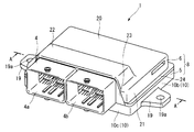
図1〜図5は、本発明に係る電子制御装置1の概略構成を模式的に示した説明図であり、図1及び図2は電子制御装置1の分解斜視図であり、図3は電子制御装置1の斜視図、図4は図3のA−A線に沿った断面図、図5は電子制御装置1の筐体8を構成するケース5の斜視図である。
Hereinafter, an embodiment of the present invention will be described in detail with reference to the drawings.
1 to 5 are explanatory views schematically showing a schematic configuration of an electronic control device 1 according to the present invention, FIGS. 1 and 2 are exploded perspective views of the electronic control device 1, and FIG. 4 is a cross-sectional view taken along line AA in FIG. 3, and FIG. 5 is a perspective view of the case 5 constituting the housing 8 of the electronic control device 1. FIG.

電子制御装置1は、例えば、自動車に搭載されてエンジンやトランスミッションあるいはブレーキ等の制御に用いられるものであって、発熱性のある電子部品2a〜2cや各種電子部品2d、2e等の電子部品2が電子部品実装面であるその表面3a及び裏面3bに複数実装された矩形板状の回路基板3と、回路基板3に取り付けられ、回路基板に形成される電気回路と外部機器とを電気的に接続するコネクタ4と、回路基板3が収容固定されるケース5と、ケース5に収容された回路基板3を覆う上側のカバー6と、電子部品2のうち回路基板3の裏面3bに実装された電子部品2a、2b、2cとケース5との間を隙間なく埋める放熱材7と、から大略構成されている。尚、回路基板3には、実際には、図示した電子部品2a〜2e以外にも、各種電子部品が複数実装されている。   The electronic control device 1 is mounted on an automobile and used for controlling an engine, a transmission, a brake, or the like. The electronic control device 1 is an electronic component 2 such as a heat-generating electronic component 2a to 2c or various electronic components 2d and 2e. Is a rectangular plate-like circuit board 3 mounted on the front surface 3a and the back surface 3b of the electronic component mounting surface, and an electric circuit attached to the circuit board 3 and formed on the circuit board and an external device are electrically connected The connector 4 to be connected, the case 5 in which the circuit board 3 is housed and fixed, the upper cover 6 that covers the circuit board 3 housed in the case 5, and the back surface 3 b of the circuit board 3 among the electronic components 2. The heat dissipating material 7 fills the space between the electronic components 2a, 2b, 2c and the case 5 without any gaps. The circuit board 3 is actually mounted with a plurality of various electronic components in addition to the illustrated electronic components 2a to 2e.

電子部品2aは、回路基板3の一端(図1における左側端)側の外周縁に複数(本実施形態では4つ)実装されている。電子部品2bは、回路基板3の一端(図1における左側端)側で、電子部品2aよりも内周側となる位置に複数(本実施形態では4つ)実装されている。電子部品2cは、回路基板3の一端(図1における左側端)側で、電子部品2a、2bよりも内周側となる位置に複数(本実施形態では3つ)実装されている。つまり、図2に示すように、発熱性のある電子部品2a〜2cは、回路基板3の短辺方向にそれぞれ直列に並んだ状態で、回路基板3の一端(図1における左側端)側の外周縁から内周側に向かって、電子部品2a、2b、2cの順番で並列に実装されている。   A plurality (four in this embodiment) of electronic components 2a are mounted on the outer peripheral edge of one end (the left end in FIG. 1) side of the circuit board 3. A plurality (four in this embodiment) of electronic components 2b are mounted at positions on the inner peripheral side of the electronic component 2a on one end (the left end in FIG. 1) side of the circuit board 3. A plurality (three in this embodiment) of electronic components 2c are mounted on the inner peripheral side of the electronic components 2a and 2b on one end (the left end in FIG. 1) side of the circuit board 3. That is, as shown in FIG. 2, the heat-generating electronic components 2 a to 2 c are arranged in series in the short side direction of the circuit board 3, and are arranged on one end (the left end in FIG. 1) side of the circuit board 3. The electronic components 2a, 2b, and 2c are mounted in parallel in the order from the outer peripheral edge toward the inner peripheral side.

回路基板3に実装される電子部品2としては、例えば、IC、FET(電界効果トランジスタ)、MOSFET(酸化膜半導体電界効果トランジスタ)、トランジスタ、コンデンサ、ダイオード、抵抗等が挙げられる。   Examples of the electronic component 2 mounted on the circuit board 3 include an IC, an FET (field effect transistor), a MOSFET (oxide film semiconductor field effect transistor), a transistor, a capacitor, a diode, and a resistor.

回路基板3は、例えば、ガラスエポキシ樹脂等からなり、回路基板3の表面3aに、外部のコネクタ(図示外)とそれぞれ接続される2つ接続口4a、4bを有するコネクタ4が取り付けられている。尚、本実施形態では、回路基板3の裏面3b側がケース5に対する取付面となっている。   The circuit board 3 is made of, for example, glass epoxy resin, and a connector 4 having two connection ports 4a and 4b connected to external connectors (not shown) is attached to the surface 3a of the circuit board 3, respectively. . In the present embodiment, the back surface 3 b side of the circuit board 3 is an attachment surface for the case 5.

また、回路基板3は、その外周縁の4隅が、ねじ18によってケース5の回路基板支持部11(後述)に固定されている。尚、回路基板3をケース5に対して接着材で固定することも可能である。   The circuit board 3 has four corners on the outer peripheral edge thereof fixed to a circuit board support portion 11 (described later) of the case 5 by screws 18. The circuit board 3 can be fixed to the case 5 with an adhesive.

ケース5及びカバー6は、電子制御装置1の筐体8を構成するものであって、ケース5は略矩形の皿形状を呈し、カバー6はケース5よりも深底となる略矩形の皿形状を呈している。   The case 5 and the cover 6 constitute the housing 8 of the electronic control device 1, and the case 5 has a substantially rectangular dish shape, and the cover 6 has a substantially rectangular dish shape deeper than the case 5. Presents.

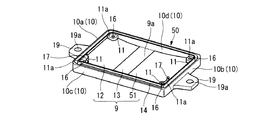
ケース5は、アルミや鉄等の放熱性に優れた金属材料によって形成されており、図5に示すように、筐体8の基板対向壁に相当する略矩形板状の底壁9と、底壁9の外周縁に立設された側壁10と、その上端面11aで回路基板3を支持する回路基板支持部11と、を有している。尚、側壁10は、底壁9の短辺方向に沿った側壁10a、10bと、底壁9の長辺方向に沿った側壁10c、10dとから大略構成されている。   The case 5 is made of a metal material having excellent heat dissipation such as aluminum or iron. As shown in FIG. 5, the case 5 has a substantially rectangular plate-like bottom wall 9 corresponding to the substrate facing wall of the housing 8, and a bottom It has a side wall 10 erected on the outer peripheral edge of the wall 9 and a circuit board support portion 11 that supports the circuit board 3 with its upper end surface 11a. The side wall 10 is generally composed of side walls 10 a and 10 b along the short side direction of the bottom wall 9 and side walls 10 c and 10 d along the long side direction of the bottom wall 9.

底壁9は、回路基板3の裏面3bと対向しており、回路基板支持部11に近づくほど、回路基板3の裏面3bとのクリアランスCが小さくなるように形成されたクリアランス変化部12と、回路基板支持部11との位置関係に関わらず回路基板3の裏面3bとのクリアランスCが一定となるクリアランス一定部13と、を有している。   The bottom wall 9 faces the back surface 3b of the circuit board 3, and the clearance changing portion 12 formed so that the clearance C from the back surface 3b of the circuit board 3 becomes smaller as the circuit board support portion 11 is approached. Regardless of the positional relationship with the circuit board support part 11, there is a constant clearance part 13 where the clearance C with the back surface 3 b of the circuit board 3 is constant.

クリアランス変化部12は、回路基板3の裏面3bに実装された電子部品2a〜2cと対向する部分に形成されている。詳述すれば、底壁9の片側(図1に左側)に、底壁9の短辺方向の全長に亙ってクリアランス変化部12が形成されている。   The clearance changing portion 12 is formed in a portion facing the electronic components 2 a to 2 c mounted on the back surface 3 b of the circuit board 3. More specifically, the clearance changing portion 12 is formed on one side (left side in FIG. 1) of the bottom wall 9 over the entire length of the bottom wall 9 in the short side direction.

クリアランス変化部12において、底壁9の内壁面9aは、回路基板3の裏面3bに対して凹となり、ケース5の側壁10aに近づくほど、回路基板3の裏面3bとのクリアランスCが小さくなる。したがって、クリアランス変化部12においては、回路基板支持部11に近づくほど、底壁9の内壁面9aと、回路基板3の裏面3bとのクリアランスCが概して小さくなる。   In the clearance changing portion 12, the inner wall surface 9 a of the bottom wall 9 is concave with respect to the back surface 3 b of the circuit board 3, and the clearance C from the back surface 3 b of the circuit board 3 decreases as the side wall 10 a of the case 5 approaches. Therefore, in the clearance changing portion 12, the clearance C between the inner wall surface 9 a of the bottom wall 9 and the back surface 3 b of the circuit board 3 generally becomes smaller as the circuit board support portion 11 is approached.

尚、本実施形態のクリアランス変化部12においては、底壁9の長辺方向の位置(側壁10aからの距離)が同じであれば、底壁9の短辺方向の位置(側壁10cまたは10dからの距離)が異なっていても、底壁9の内壁面9aと回路基板3の裏面3bとのクリアランスCは同じとなる。   In the clearance changing portion 12 of the present embodiment, if the position of the bottom wall 9 in the long side direction (distance from the side wall 10a) is the same, the position of the bottom wall 9 in the short side direction (from the side wall 10c or 10d). Are different, the clearance C between the inner wall surface 9a of the bottom wall 9 and the back surface 3b of the circuit board 3 is the same.

底壁9のクリアランス変化部12以外の部分はクリアランス一定部13となっている。クリアランス一定部13において、底壁9の内壁面9aは、ケース5に固定された状態の回路基板3の裏面3bと平行となる平面となる。   A portion other than the clearance changing portion 12 of the bottom wall 9 is a constant clearance portion 13. In the constant clearance portion 13, the inner wall surface 9 a of the bottom wall 9 becomes a plane parallel to the back surface 3 b of the circuit board 3 fixed to the case 5.

側壁10の先端には、側壁10の全周に亙って連続する溝14が形成されている。この溝14には、接着材15(後述の図4を参照)が充填され、カバー6に設けられた突条25(後述)や、コネクタ4に設けられた係合突片4c、4cの先端側が挿入されることで、ケース5とカバー6とが接着固定され、溝14から筐体8内に水分や塵埃等の異物が侵入しないように液密にシールされる。また、カバー6に設けられた切欠部23(後述)と、コネクタ4とが当接する部分にも接着材(図示せず)が塗布されており、この当接部分から筐体8内に水分や塵埃等の異物が侵入しないように液密にシールされる。   A groove 14 that is continuous over the entire circumference of the side wall 10 is formed at the tip of the side wall 10. The groove 14 is filled with an adhesive material 15 (see FIG. 4 to be described later), and protrusions 25 (described later) provided on the cover 6 and the tips of engaging protrusions 4 c and 4 c provided on the connector 4. By inserting the side, the case 5 and the cover 6 are bonded and fixed, and are sealed fluid-tight so that foreign matter such as moisture and dust does not enter the housing 8 from the groove 14. An adhesive (not shown) is also applied to a portion where a notch 23 (described later) provided in the cover 6 and a connector 4 abut, and moisture or moisture is applied from the abutting portion into the housing 8. It is sealed fluid-tight so that foreign matter such as dust does not enter.

回路基板支持部11は、底壁9の4隅から側壁10に沿って突出する柱状の台座であり、全長に亙って側壁10に対して連結されている。換言すれば、回路基板支持部11は、側壁10からケース5の内側に向かって突出した(張り出した)柱状の台座である。   The circuit board support part 11 is a columnar pedestal that protrudes from the four corners of the bottom wall 9 along the side wall 10 and is connected to the side wall 10 over the entire length. In other words, the circuit board support portion 11 is a columnar pedestal that protrudes (protrudes) from the side wall 10 toward the inside of the case 5.

この回路基板支持部11は、その上端面11aに回路基板3を載せることで、ケース5内における回路基板3の上下方向(後述する図4における上下方向)の位置決めが行われる。   The circuit board support portion 11 is positioned in the vertical direction (vertical direction in FIG. 4 described later) of the circuit board 3 in the case 5 by placing the circuit board 3 on the upper end surface 11a.

また、回路基板支持部11の上端面11aには、回路基板3をケース5に対して固定するねじ18が螺合するねじ穴16が形成されている。そして、4つある回路基板支持部11のうちの2つの回路基板支持部11の上端面11aには、回路基板3の外周縁に形成された切欠穴3cと係合し、ケース5内における回路基板3の水平方向の位置決めを行う位置決め突起17がそれぞれ形成されている。   In addition, a screw hole 16 is formed in the upper end surface 11 a of the circuit board support 11 to which a screw 18 for fixing the circuit board 3 to the case 5 is screwed. Of the four circuit board support parts 11, the upper end surface 11 a of the two circuit board support parts 11 engages with the notch hole 3 c formed in the outer peripheral edge of the circuit board 3, and the circuit in the case 5 Positioning protrusions 17 for positioning the substrate 3 in the horizontal direction are formed.

また、ケース5には、電子制御装置1の車体(図示外)への取り付けのため一対のブラケット19、19が一体に設けられている。本実施形態では、各ブラケット19、19にそれぞれ設けられた上下方向に貫通する貫通穴19a、19aにより、電子制御装置1の前記車体への取り付けが行われる。   The case 5 is integrally provided with a pair of brackets 19 and 19 for mounting the electronic control device 1 to a vehicle body (not shown). In the present embodiment, the electronic control device 1 is attached to the vehicle body by through holes 19a and 19a penetrating vertically in the brackets 19 and 19, respectively.

カバー6は、金属または樹脂材料によって形成されており、略矩形板状の上壁20と、上壁20の外周縁に立設された側壁21と、コネクタ4の外形状に合わせて上壁20から突出したコネクタ収容部22と、コネクタ4の一端を外部に臨ませるために側壁21の一部を切り欠いて形成された切欠部23と、側壁21の先端側に設けられた鍔状のフランジ部24と、フランジ部24に形成され、ケース5との組み付け時には側壁10先端の溝14に係合する突条25と、を有している。切欠部23により、ケース5にカバー6を組み付けた際に、筐体8の一側面に開口が形成され、この開口からコネクタ4の一端が外部に突出可能となる。   The cover 6 is made of a metal or a resin material, and has a substantially rectangular plate-shaped upper wall 20, a side wall 21 erected on the outer peripheral edge of the upper wall 20, and an upper wall 20 according to the outer shape of the connector 4. A connector housing portion 22 protruding from the side, a cutout portion 23 formed by cutting out a part of the side wall 21 so that one end of the connector 4 faces the outside, and a flange-like flange provided on the front end side of the side wall 21 And a protrusion 25 that is formed in the flange portion 24 and engages with the groove 14 at the tip of the side wall 10 when assembled with the case 5. When the cover 6 is assembled to the case 5 by the cutout portion 23, an opening is formed on one side surface of the housing 8, and one end of the connector 4 can protrude to the outside from this opening.

放熱材7は、回路基板3の裏面3bに実装された複数の電子部品2a〜2cで発生した熱を、ケース5の底壁9に対して伝導するよう設けられている。この放熱材7は、例えばシリコンを基材とした放熱グリスであって、絶縁性を有している。尚、放熱材7としては、ケース5に対して回路基板3を組み付ける際には、液状あるいはペースト状で、組み付け後に固化するものが好ましい。   The heat dissipating material 7 is provided so as to conduct heat generated by the plurality of electronic components 2 a to 2 c mounted on the back surface 3 b of the circuit board 3 to the bottom wall 9 of the case 5. The heat dissipating material 7 is a heat dissipating grease based on, for example, silicon, and has an insulating property. In addition, when the circuit board 3 is assembled to the case 5, the heat radiating material 7 is preferably liquid or pasty and solidified after assembly.

ここで、外力、周囲の温度変化、周囲の圧力変化等の影響を受けて回路基板3もしくは筐体8が変形した場合でも、回路基板支持部11では回路基板3の筐体8内の位置が拘束されほとんど不変なので、筐体8に対する固定点である回路基板支持部11に近いほど、回路基板3の電子部品実装面と直交する方向における電子部品実装面と基板対向壁の内壁面とのクリアランスCの変化量は小さくなる。すなわち、回路基板支持部11では筐体8内の位置が拘束されほとんど不変なので、外力、周囲の温度変化、周囲の圧力変化等の影響を受けて回路基板3もしくは筐体8が変形した場合でも、筐体8に対する固定点である回路基板支持部11に近いほど、回路基板3と直交する方向における裏面3bと底壁9の内壁面9aとのクリアランスCの変化量は小さくなる。   Here, even when the circuit board 3 or the housing 8 is deformed by the influence of external force, ambient temperature change, ambient pressure change, etc., the position of the circuit board 3 in the housing 8 remains at the circuit board support portion 11. Since it is restrained and almost unchanged, the clearance between the electronic component mounting surface and the inner wall surface of the substrate facing wall in the direction orthogonal to the electronic component mounting surface of the circuit board 3 is closer to the circuit board support portion 11 that is a fixed point with respect to the housing 8. The amount of change in C is small. That is, since the position in the housing 8 is constrained and almost unchanged in the circuit board support part 11, even when the circuit board 3 or the housing 8 is deformed by the influence of external force, ambient temperature change, ambient pressure change, etc. The closer to the circuit board support portion 11, which is a fixed point with respect to the housing 8, the smaller the amount of change in the clearance C between the back surface 3 b and the inner wall surface 9 a of the bottom wall 9 in the direction orthogonal to the circuit board 3.

また、回路基板3の裏面3bに実装された電子部品2a〜2cと、回路基板3の裏面3bと対向する底壁9の内壁面9aとのクリアランスCは、回路基板3もしくは筐体8が変形しても各電子部品2a〜2cがそれぞれケース5の底壁9に対して接触しないように設定する必要があるが、これによって、クリアランス変化部12においては、回路基板支持部11に近接して実装された電子部品2aほど、基板対向壁である底壁9とのクリアランスCを小さくすることが可能となる。   The clearance C between the electronic components 2a to 2c mounted on the back surface 3b of the circuit board 3 and the inner wall surface 9a of the bottom wall 9 facing the back surface 3b of the circuit board 3 is deformed by the circuit board 3 or the casing 8. Even so, it is necessary to set the electronic components 2 a to 2 c so as not to contact the bottom wall 9 of the case 5, but in this way, the clearance changing portion 12 is close to the circuit board support portion 11. The closer the mounted electronic component 2a is, the smaller the clearance C from the bottom wall 9 which is the substrate facing wall can be made.

尚、上述したクリアランスCの変化量は、回路基板3の変形のほか、筐体8の構造によっても変化する。例えば、ケース5にリブ等の補強部位を設けられている場合には、この補強部位によってケース5の剛性が変化(向上)することになるため、補強部位の有無も考慮してクリアランスCを設定すればよい。また、回路基板3において、コネクタ4が取り付けられる部分は、コネクタ4からの多数のピンが固定されるため、相対的に剛性が高くなっているものの、コネクタ4に接続される外部のコネクタや、外部のコネクタに接続された配線等に作用した応力によってこじられると、それによってクリアランスCの変化量が大きくなる可能性がある。したがって、回路基板3のうち、コネクタ4が取り付けられる部分については、クリアランスCを設定する際に、外部からの応力の入力によりクリアランスCの変化量が大きい位置であること考慮しておけばよい。つまり、回路基板3のうち、コネクタ4が取り付けられる部分は、コネクタ4に対して入力が予想される外部からの応力の大きさに応じて、クリアランスCを設定すればよい。   The amount of change in the clearance C described above varies depending on the structure of the housing 8 in addition to the deformation of the circuit board 3. For example, when the case 5 is provided with a reinforcing part such as a rib, the rigidity of the case 5 changes (improves) by the reinforcing part, and therefore the clearance C is set in consideration of the presence or absence of the reinforcing part. do it. Further, in the circuit board 3, the portion to which the connector 4 is attached has a relatively high rigidity because a large number of pins from the connector 4 are fixed, but an external connector connected to the connector 4, If it is distorted by the stress acting on the wiring connected to the external connector, the amount of change in the clearance C may increase. Therefore, regarding the portion of the circuit board 3 to which the connector 4 is attached, when setting the clearance C, it is only necessary to consider that the amount of change in the clearance C is large due to external stress input. That is, in the portion of the circuit board 3 to which the connector 4 is attached, the clearance C may be set according to the magnitude of external stress expected to be input to the connector 4.

図6に示す比較例の電子制御装置30にように、ケース5の底壁9にクリアランス変化部12が設定されていない構成では、回路基板3と直交する方向において、回路基板3の裏面3bと底壁9の内壁面9aとのクリアランスCの変化量が最も大きい位置(ケース5の中央)となる回路基板支持部11から最も離れた位置を基準に、電子部品2a〜2cと、これら電子部品2a〜2cに対向する底壁9の内壁面9aとのクリアランスCをそれぞれ設定すると、回路基板支持部11に近い電子部品2a、2bにおいては、底壁9の内壁面9aとのクリアランスCが必要以上に大きくなってしまい、放熱性能が悪化してしまうことになる。   In the configuration in which the clearance changing portion 12 is not set on the bottom wall 9 of the case 5 as in the electronic control device 30 of the comparative example shown in FIG. 6, the back surface 3 b of the circuit board 3 is arranged in the direction orthogonal to the circuit board 3. The electronic components 2a to 2c and these electronic components based on the position farthest from the circuit board support portion 11 that is the position where the change amount of the clearance C with the inner wall surface 9a of the bottom wall 9 is the largest (center of the case 5). If the clearance C with the inner wall surface 9a of the bottom wall 9 facing 2a to 2c is set, in the electronic components 2a and 2b close to the circuit board support portion 11, a clearance C with the inner wall surface 9a of the bottom wall 9 is required. As a result, the heat dissipation performance is deteriorated.

詳述すると、回路基板3と直交する方向における回路基板3の裏面3bと底壁9の内壁面9aとのクリアランスCの最大変化量δを考えた場合、回路基板支持部11から離れるほど最大変化量δも大きくなるため、図5中に矢示するように、回路基板支持部11に近い回路基板3の外周縁におけるクリアランスCの最大変化量δ1に比べて、ケース5の中央に位置における最大変化量δ2が相対的に大きくなる。したがって、回路基板3の裏面3bにおいては、ケース5の中央に位置においてクリアランスCの変化量が最大となったときに(最大変化量δ2のときに)、最も内側に位置する(回路基板支持部11から最も離れた)電子部品2cが底壁9の内壁面9aに対して接触しないように、各電子部品2a〜2cと底壁9の内壁面9aとのクリアランスCが決定されることになるため、回路基板支持部11に近い電子部品2a、2bにおいては、底壁9の内壁面9aとのクリアランスCが必要以上に大きくなってしまい、放熱性能が悪化してしまうことになる。   More specifically, when the maximum amount of change δ of the clearance C between the back surface 3b of the circuit board 3 and the inner wall surface 9a of the bottom wall 9 in the direction orthogonal to the circuit board 3 is considered, the maximum change as the distance from the circuit board support 11 increases. Since the amount δ also increases, as shown by an arrow in FIG. 5, the maximum amount at the position in the center of the case 5 is larger than the maximum change amount δ1 of the clearance C at the outer peripheral edge of the circuit board 3 near the circuit board support 11. The amount of change δ2 becomes relatively large. Therefore, the back surface 3b of the circuit board 3 is located on the innermost side (when the maximum change amount δ2) when the change amount of the clearance C is maximized at the center of the case 5 (the circuit board support portion). The clearance C between each of the electronic components 2a to 2c and the inner wall surface 9a of the bottom wall 9 is determined so that the electronic component 2c (the furthest away from 11) does not contact the inner wall surface 9a of the bottom wall 9. Therefore, in the electronic components 2a and 2b close to the circuit board support portion 11, the clearance C between the bottom wall 9 and the inner wall surface 9a becomes larger than necessary, and the heat dissipation performance is deteriorated.

尚、図6に示す比較例の電子制御装置30は、上述した実施形態におけるケース5の底壁9にクリアランス変化部12を設定していないものを模式的に示したものであり、上述した図4と同一の構成要素については同一の符号を付し、重複する説明を省略する。また、この比較例においても、回路基板支持部11は底壁9の4隅にのみ設けられている。   Note that the electronic control device 30 of the comparative example shown in FIG. 6 schematically shows the case where the clearance changing portion 12 is not set on the bottom wall 9 of the case 5 in the above-described embodiment. Constituent elements identical to those in FIG. Also in this comparative example, the circuit board support portions 11 are provided only at the four corners of the bottom wall 9.

一方、上述した本実施形態の電子制御装置1においては、ケース5の底壁9に形成されたクリアランス変化部12により、ケース5の側壁10aに近づくほど、底壁9の内壁面9aと回路基板3の裏面3bとのクリアランスCが小さくなるため、ケース5の側壁10a側に位置する電子部品2aほど、底壁9の内壁面9aとのクリアランスCを小さくすることが可能となる。すなわち、クリアランス変化部12においては、回路基板支持部11に近い位置ほど、底壁9の内壁面9aと回路基板3の裏面3bとのクリアランスCが概して小さくなるため、回路基板支持部11に近づくほど、各電子部品2a〜2cと底壁9の内壁面9aとのクリアランスCを小さく設定することが可能となる。   On the other hand, in the electronic control device 1 of the present embodiment described above, the inner wall surface 9a of the bottom wall 9 and the circuit board become closer to the side wall 10a of the case 5 by the clearance changing portion 12 formed on the bottom wall 9 of the case 5. 3, the clearance C between the bottom wall 9 and the inner wall surface 9 a of the electronic component 2 a located on the side wall 10 a side of the case 5 can be reduced. That is, in the clearance changing portion 12, the closer to the circuit board support portion 11, the smaller the clearance C between the inner wall surface 9 a of the bottom wall 9 and the back surface 3 b of the circuit board 3, and thus the closer to the circuit board support portion 11. Thus, the clearance C between the electronic components 2a to 2c and the inner wall surface 9a of the bottom wall 9 can be set small.

したがって、クリアランス変化部12においては、各電子部品2a〜2cと底壁9の内壁面9aとのクリアランスCが必要以上に大きくなってしまい、各電子部品2a〜2cの放熱性能が悪化してしまうことを抑制することができる。また、各電子部品2a〜2cと底壁9の内壁面9aとの間に介在させる放熱材7の使用量を相対的に削減することが可能となり、総じて電子制御装置1のコスト低減を実現することができる。   Accordingly, in the clearance changing portion 12, the clearance C between the electronic components 2a to 2c and the inner wall surface 9a of the bottom wall 9 becomes larger than necessary, and the heat dissipation performance of the electronic components 2a to 2c is deteriorated. This can be suppressed. In addition, it is possible to relatively reduce the amount of use of the heat dissipating material 7 interposed between each of the electronic components 2a to 2c and the inner wall surface 9a of the bottom wall 9, and the overall cost reduction of the electronic control device 1 is realized. be able to.

尚、上述して実施形態においては、クリアランス変化部12における底壁9の内壁面9aを球面によって定義される曲面とすることも可能である。この場合には、各電子部品2a〜2cと底壁9の内壁面9aとのクリアランスCを、回路基板支持部11からの距離に応じてより厳密に設定することが可能となる。   In the above-described embodiment, the inner wall surface 9a of the bottom wall 9 in the clearance changing portion 12 can be a curved surface defined by a spherical surface. In this case, the clearance C between the electronic components 2a to 2c and the inner wall surface 9a of the bottom wall 9 can be set more strictly according to the distance from the circuit board support portion 11.

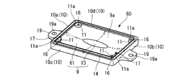
また、クリアランス変化部12は、回路基板3の裏面3bに実装される電子部品2の位置や数等に応じて適宜設定することが可能であり、例えば、回路基板支持部11が底壁9の4隅にのみある場合には、図7〜図9に示すように形成することも可能である。   Further, the clearance changing portion 12 can be appropriately set according to the position and number of the electronic components 2 mounted on the back surface 3 b of the circuit board 3. For example, the circuit board support portion 11 is provided on the bottom wall 9. If there are only four corners, they can be formed as shown in FIGS.

図7に示す第2実施形態のケース40では、底壁9の片側(図1に左側)の一部分に、底壁9のクリアランス変化部41が形成されている。   In the case 40 of the second embodiment shown in FIG. 7, a clearance changing portion 41 of the bottom wall 9 is formed on a part of one side of the bottom wall 9 (left side in FIG. 1).

クリアランス変化部41は、回路基板支持部11に近づくほど、回路基板3の裏面3bとのクリアランスが小さくなるように形成されている。つまり、クリアランス変化部41において、底壁9の内壁面9aは、回路基板3の裏面3bに対して凹となり、ケース5の側壁10aに近づくほど、回路基板3の裏面3bとのクリアランスが小さくなる。したがって、クリアランス変化部41においては、回路基板支持部11に近づくほど、底壁9の内壁面9aと、回路基板3の裏面3bとのクリアランスが概して小さくなる。   The clearance changing portion 41 is formed such that the closer to the circuit board support portion 11, the smaller the clearance from the back surface 3 b of the circuit board 3. That is, in the clearance changing portion 41, the inner wall surface 9 a of the bottom wall 9 is concave with respect to the back surface 3 b of the circuit board 3, and the clearance from the back surface 3 b of the circuit board 3 decreases as the side wall 10 a of the case 5 approaches. . Therefore, in the clearance changing portion 41, the clearance between the inner wall surface 9 a of the bottom wall 9 and the back surface 3 b of the circuit board 3 generally becomes smaller as the circuit board support portion 11 is approached.

図8に示す第3実施形態のケース50では、底壁9の両側(図1に左側及び右側)に、底壁9の短辺方向の全長に亙ってクリアランス変化部12、51が形成されている。クリアランス変化部51は、回路基板支持部11に近づくほど、回路基板3の裏面3bとのクリアランスが小さくなるように形成されている。つまり、クリアランス変化部51において、底壁9の内壁面9aは、回路基板3の裏面3bに対して凹となり、ケース5の側壁10bに近づくほど、回路基板3の裏面3bとのクリアランスが小さくなる。したがって、クリアランス変化部51においては、回路基板支持部11に近づくほど、底壁9の内壁面9aと回路基板3の裏面3bとのクリアランスが概して小さくなる。   In the case 50 of the third embodiment shown in FIG. 8, clearance changing portions 12 and 51 are formed on both sides of the bottom wall 9 (on the left and right sides in FIG. 1) over the entire length in the short side direction of the bottom wall 9. ing. The clearance changing portion 51 is formed such that the closer to the circuit board support portion 11, the smaller the clearance from the back surface 3 b of the circuit board 3. That is, in the clearance changing portion 51, the inner wall surface 9 a of the bottom wall 9 is concave with respect to the back surface 3 b of the circuit board 3, and the clearance from the back surface 3 b of the circuit board 3 decreases as the side wall 10 b of the case 5 approaches. . Accordingly, in the clearance changing portion 51, the clearance between the inner wall surface 9 a of the bottom wall 9 and the back surface 3 b of the circuit board 3 generally becomes smaller as the circuit board support portion 11 is approached.

図9に示す第4実施形態のケース60では、クリアランス変化部61が、ケース5の底壁9の略全体に形成されている。そして、クリアランス変化部61において、底壁9の内壁面9aは、球面によって定義される曲面となっている。つまり、クリアランス変化部61においては、回路基板支持部11に近づくほど、底壁9の内壁面9aと、回路基板3の裏面3bとのクリアランスが小さくなる。   In the case 60 of the fourth embodiment shown in FIG. 9, the clearance changing portion 61 is formed on substantially the entire bottom wall 9 of the case 5. In the clearance changing portion 61, the inner wall surface 9a of the bottom wall 9 is a curved surface defined by a spherical surface. That is, in the clearance changing portion 61, the closer to the circuit board support portion 11, the smaller the clearance between the inner wall surface 9 a of the bottom wall 9 and the back surface 3 b of the circuit board 3.

上述した各実施形態から把握し得る前記請求項以外の発明の技術的思想について以下に列記する。   The technical ideas of the invention other than the claims that can be understood from the above-described embodiments are listed below.

[請求項a]
前記クリアランス変化部は、前記基板対向壁の片側に形成されていることを特徴とする請求項1〜3のいずれかに記載の電子制御装置。
[Claim a]
The electronic control apparatus according to claim 1, wherein the clearance changing portion is formed on one side of the substrate facing wall.

[請求項b]
前記クリアランス変化部は、前記基板対向壁の両側に形成されていることを特徴とする請求項1〜3のいずれかに記載の電子制御装置。
[Claim b]
The electronic control device according to claim 1, wherein the clearance changing portion is formed on both sides of the substrate facing wall.

[請求項c]
前記クリアランス変化部において、前記基板対向壁の内壁面は、球面によって定義される曲面であることを特徴とする請求項3、a、bのいずれかに記載の電子制御装置。
[Claim c]
The electronic control device according to claim 3, wherein an inner wall surface of the substrate facing wall in the clearance changing portion is a curved surface defined by a spherical surface.

[請求項d]
前記クリアランス変化部は、前記基板対向壁の全体に形成され、前記基板対向壁の内壁面は、球面によって定義される曲面であることを特徴とする請求項3に記載の電子制御装置。
[Claim d]
The electronic control device according to claim 3, wherein the clearance changing portion is formed on the entire substrate facing wall, and an inner wall surface of the substrate facing wall is a curved surface defined by a spherical surface.

[請求項e]
前記クリアランス変化部において、前記基板対向壁の内壁面は、電子部品実装面に対して所定の角度で傾いた平面によって定義される傾斜面であることを特徴とする請求項1または2に記載の電子制御装置。
[Claim e]
3. The clearance changing portion according to claim 1, wherein the inner wall surface of the substrate facing wall is an inclined surface defined by a plane inclined at a predetermined angle with respect to the electronic component mounting surface. Electronic control device.

1…電子制御装置
2a…電子部品
2b…電子部品
2c…電子部品
3…回路基板
3b…裏面
5…ケース
6…カバー
7…放熱材
8…筐体
9…底壁
10…側壁
11…回路基板支持部
12…クリアランス変化部
DESCRIPTION OF SYMBOLS 1 ... Electronic control apparatus 2a ... Electronic component 2b ... Electronic component 2c ... Electronic component 3 ... Circuit board 3b ... Back surface 5 ... Case 6 ... Cover 7 ... Radiating material 8 ... Housing 9 ... Bottom wall 10 ... Side wall 11 ... Circuit board support Part 12 ... Clearance changing part

Claims (3)

発熱性のある電子部品が実装された回路基板と、
前記回路基板が収容された筐体と、を有する電子制御装置において、
前記筐体は、前記回路基板の電子部品実装面に対向する基板対向壁と、当該筐体内で前記回路基板を支持固定する回路基板支持部と、を有し、
前記基板対向壁は、前記回路基板支持部に近づくほど、前記基板対向壁と前記電子部品実装面とのクリアランスが小さくなるよう形成されたクリアランス変化部を有することを特徴とする電子制御装置。
A circuit board on which heat-generating electronic components are mounted;
In an electronic control device having a housing in which the circuit board is accommodated,
The housing includes a substrate facing wall facing the electronic component mounting surface of the circuit board, and a circuit board support portion for supporting and fixing the circuit board in the housing.
The electronic control device according to claim 1, wherein the board facing wall includes a clearance changing portion formed such that a clearance between the board facing wall and the electronic component mounting surface becomes smaller as the circuit board supporting portion is approached.
前記基板対向壁は、前記回路基板支持部との位置関係に関わらず前記基板対向壁と前記電子部品実装面とのクリアランスが一定となるクリアランス一定部を有し、前記クリアランス変化部は、前記基板対向壁の一部に形成にされていることを特徴とする請求項1に記載の電子制御装置。   The substrate facing wall has a constant clearance portion where a clearance between the substrate facing wall and the electronic component mounting surface is constant regardless of a positional relationship with the circuit board support portion, and the clearance changing portion is the substrate. The electronic control device according to claim 1, wherein the electronic control device is formed on a part of the opposing wall. 前記クリアランス変化部において、前記基板対向壁の内壁面は、前記電子部品実装面に対して凹となる曲面となるよう形成されていることを特徴とする請求項1または2に記載の電子制御装置。   3. The electronic control device according to claim 1, wherein an inner wall surface of the substrate facing wall is formed to be a curved surface that is concave with respect to the electronic component mounting surface in the clearance changing portion. .
JP2011063503A 2011-03-23 2011-03-23 Electronic controller Pending JP2012199451A (en)

Priority Applications (1)

Application Number Priority Date Filing Date Title
JP2011063503A JP2012199451A (en) 2011-03-23 2011-03-23 Electronic controller

Applications Claiming Priority (1)

Application Number Priority Date Filing Date Title
JP2011063503A JP2012199451A (en) 2011-03-23 2011-03-23 Electronic controller

Publications (1)

Publication Number Publication Date
JP2012199451A true JP2012199451A (en) 2012-10-18

Family

ID=47181364

Family Applications (1)

Application Number Title Priority Date Filing Date
JP2011063503A Pending JP2012199451A (en) 2011-03-23 2011-03-23 Electronic controller

Country Status (1)

Country Link
JP (1) JP2012199451A (en)

Cited By (1)

* Cited by examiner, † Cited by third party
Publication number Priority date Publication date Assignee Title
JP2015050824A (en) * 2013-08-30 2015-03-16 株式会社ケーヒン Vehicle electronic control device

Citations (3)

* Cited by examiner, † Cited by third party
Publication number Priority date Publication date Assignee Title
JP2000174468A (en) * 1998-12-02 2000-06-23 Denso Corp Cooling structure of electronic component
JP2002198671A (en) * 2000-12-26 2002-07-12 Denso Corp Cooling structure of electronic component
JP2006066623A (en) * 2004-08-26 2006-03-09 Denso Corp Electronic control apparatus

Patent Citations (3)

* Cited by examiner, † Cited by third party
Publication number Priority date Publication date Assignee Title
JP2000174468A (en) * 1998-12-02 2000-06-23 Denso Corp Cooling structure of electronic component
JP2002198671A (en) * 2000-12-26 2002-07-12 Denso Corp Cooling structure of electronic component
JP2006066623A (en) * 2004-08-26 2006-03-09 Denso Corp Electronic control apparatus

Cited By (1)

* Cited by examiner, † Cited by third party
Publication number Priority date Publication date Assignee Title
JP2015050824A (en) * 2013-08-30 2015-03-16 株式会社ケーヒン Vehicle electronic control device

Similar Documents

Publication Publication Date Title
JP5644706B2 (en) Electronic component fixing structure for electric compressor
CN107432093B (en) Electronic control unit
JP4375242B2 (en) Semiconductor heatsink
WO2014148085A1 (en) Electronic control apparatus and method for connecting substrate of electronic control apparatus
JP2014138442A (en) Motor driving device having radiator
JP2017139934A (en) Electric power conversion system
JP5846181B2 (en) Electronic control unit
US10880989B2 (en) Electrical junction box
JP2014139986A (en) Electronic controller
JP2008053635A (en) Electrical equipment unit
JP2015115533A (en) Electronic device
JP6375214B2 (en) Electronic control unit
US9798098B2 (en) Optical module
JP2007201283A (en) Electronic control device and casing therefor
JP6303981B2 (en) Electrical equipment
JP2012216871A (en) Electrical component unit
JP2012200071A (en) Motor control device
JP2014165227A (en) Electronic control device
WO2017098703A1 (en) Heat radiating device for heat generating electronic component, manufacturing method thereof, and vehicle-mounted charger
WO2013161521A1 (en) Driver-integrated motor
JP2012199451A (en) Electronic controller
JP2017162860A (en) Electronic control device
JP6307871B2 (en) Electronic control unit
JP2016063086A (en) Circuit board and electronic control device
JP2007324223A (en) Attaching structure for heating element

Legal Events

Date Code Title Description
A521 Written amendment

Free format text: JAPANESE INTERMEDIATE CODE: A523

Effective date: 20130214

A621 Written request for application examination

Free format text: JAPANESE INTERMEDIATE CODE: A621

Effective date: 20130214

A977 Report on retrieval

Free format text: JAPANESE INTERMEDIATE CODE: A971007

Effective date: 20131011

A131 Notification of reasons for refusal

Free format text: JAPANESE INTERMEDIATE CODE: A131

Effective date: 20131022

A521 Written amendment

Free format text: JAPANESE INTERMEDIATE CODE: A523

Effective date: 20131216

A131 Notification of reasons for refusal

Free format text: JAPANESE INTERMEDIATE CODE: A131

Effective date: 20140603

A521 Written amendment

Free format text: JAPANESE INTERMEDIATE CODE: A523

Effective date: 20140717

A02 Decision of refusal

Free format text: JAPANESE INTERMEDIATE CODE: A02

Effective date: 20150106