JP2012194080A - Bolometer type thz wave detector - Google Patents
Bolometer type thz wave detector Download PDFInfo
- Publication number
- JP2012194080A JP2012194080A JP2011058693A JP2011058693A JP2012194080A JP 2012194080 A JP2012194080 A JP 2012194080A JP 2011058693 A JP2011058693 A JP 2011058693A JP 2011058693 A JP2011058693 A JP 2011058693A JP 2012194080 A JP2012194080 A JP 2012194080A
- Authority
- JP
- Japan
- Prior art keywords
- film
- thz wave
- bolometer
- temperature detection
- wave detector
- Prior art date
- Legal status (The legal status is an assumption and is not a legal conclusion. Google has not performed a legal analysis and makes no representation as to the accuracy of the status listed.)
- Pending
Links
- 239000010408 film Substances 0.000 claims abstract description 200
- 239000010409 thin film Substances 0.000 claims abstract description 24
- 239000000758 substrate Substances 0.000 claims abstract description 13
- 230000003287 optical effect Effects 0.000 claims abstract description 9
- 238000009429 electrical wiring Methods 0.000 claims abstract description 8
- 238000001514 detection method Methods 0.000 claims description 53
- 238000010521 absorption reaction Methods 0.000 claims description 38
- 230000002093 peripheral effect Effects 0.000 claims description 4
- 238000004519 manufacturing process Methods 0.000 abstract description 20
- 238000002955 isolation Methods 0.000 abstract 1
- 230000001681 protective effect Effects 0.000 description 95
- 239000010410 layer Substances 0.000 description 27
- 229910052581 Si3N4 Inorganic materials 0.000 description 13
- HQVNEWCFYHHQES-UHFFFAOYSA-N silicon nitride Chemical compound N12[Si]34N5[Si]62N3[Si]51N64 HQVNEWCFYHHQES-UHFFFAOYSA-N 0.000 description 13
- 229920001721 polyimide Polymers 0.000 description 9
- VYPSYNLAJGMNEJ-UHFFFAOYSA-N Silicium dioxide Chemical compound O=[Si]=O VYPSYNLAJGMNEJ-UHFFFAOYSA-N 0.000 description 8
- 238000010586 diagram Methods 0.000 description 8
- 229910052751 metal Inorganic materials 0.000 description 8
- 239000002184 metal Substances 0.000 description 8
- 229910052814 silicon oxide Inorganic materials 0.000 description 8
- 239000004642 Polyimide Substances 0.000 description 7
- 229910052782 aluminium Inorganic materials 0.000 description 7
- 239000000463 material Substances 0.000 description 7
- 239000010936 titanium Substances 0.000 description 7
- 229910052719 titanium Inorganic materials 0.000 description 7
- 229910004298 SiO 2 Inorganic materials 0.000 description 6
- XUIMIQQOPSSXEZ-UHFFFAOYSA-N Silicon Chemical compound [Si] XUIMIQQOPSSXEZ-UHFFFAOYSA-N 0.000 description 6
- 230000002950 deficient Effects 0.000 description 6
- 238000010438 heat treatment Methods 0.000 description 6
- 229910052710 silicon Inorganic materials 0.000 description 6
- 239000010703 silicon Substances 0.000 description 6
- LIVNPJMFVYWSIS-UHFFFAOYSA-N silicon monoxide Chemical compound [Si-]#[O+] LIVNPJMFVYWSIS-UHFFFAOYSA-N 0.000 description 6
- 239000007789 gas Substances 0.000 description 5
- 238000004544 sputter deposition Methods 0.000 description 5
- NBIIXXVUZAFLBC-UHFFFAOYSA-N Phosphoric acid Chemical compound OP(O)(O)=O NBIIXXVUZAFLBC-UHFFFAOYSA-N 0.000 description 4
- 238000004364 calculation method Methods 0.000 description 4
- 238000000151 deposition Methods 0.000 description 4
- 238000000034 method Methods 0.000 description 4
- 238000005268 plasma chemical vapour deposition Methods 0.000 description 4
- 230000007261 regionalization Effects 0.000 description 4
- WGTYBPLFGIVFAS-UHFFFAOYSA-M tetramethylammonium hydroxide Chemical compound [OH-].C[N+](C)(C)C WGTYBPLFGIVFAS-UHFFFAOYSA-M 0.000 description 4
- 238000001039 wet etching Methods 0.000 description 4
- 238000004380 ashing Methods 0.000 description 3
- QVGXLLKOCUKJST-UHFFFAOYSA-N atomic oxygen Chemical compound [O] QVGXLLKOCUKJST-UHFFFAOYSA-N 0.000 description 3
- 230000015572 biosynthetic process Effects 0.000 description 3
- 230000018109 developmental process Effects 0.000 description 3
- 239000011810 insulating material Substances 0.000 description 3
- 239000001301 oxygen Substances 0.000 description 3
- 229910052760 oxygen Inorganic materials 0.000 description 3
- OGIDPMRJRNCKJF-UHFFFAOYSA-N titanium oxide Inorganic materials [Ti]=O OGIDPMRJRNCKJF-UHFFFAOYSA-N 0.000 description 3
- KRHYYFGTRYWZRS-UHFFFAOYSA-N Fluorane Chemical compound F KRHYYFGTRYWZRS-UHFFFAOYSA-N 0.000 description 2
- OAKJQQAXSVQMHS-UHFFFAOYSA-N Hydrazine Chemical compound NN OAKJQQAXSVQMHS-UHFFFAOYSA-N 0.000 description 2
- VEXZGXHMUGYJMC-UHFFFAOYSA-N Hydrochloric acid Chemical compound Cl VEXZGXHMUGYJMC-UHFFFAOYSA-N 0.000 description 2
- GWEVSGVZZGPLCZ-UHFFFAOYSA-N Titan oxide Chemical compound O=[Ti]=O GWEVSGVZZGPLCZ-UHFFFAOYSA-N 0.000 description 2
- XHCLAFWTIXFWPH-UHFFFAOYSA-N [O-2].[O-2].[O-2].[O-2].[O-2].[V+5].[V+5] Chemical compound [O-2].[O-2].[O-2].[O-2].[O-2].[V+5].[V+5] XHCLAFWTIXFWPH-UHFFFAOYSA-N 0.000 description 2
- 229910000147 aluminium phosphate Inorganic materials 0.000 description 2
- NBVXSUQYWXRMNV-UHFFFAOYSA-N monofluoromethane Natural products FC NBVXSUQYWXRMNV-UHFFFAOYSA-N 0.000 description 2
- 238000001020 plasma etching Methods 0.000 description 2
- 229910021420 polycrystalline silicon Inorganic materials 0.000 description 2
- 229920005591 polysilicon Polymers 0.000 description 2
- 239000004065 semiconductor Substances 0.000 description 2
- 230000035945 sensitivity Effects 0.000 description 2
- 238000000926 separation method Methods 0.000 description 2
- 229910001935 vanadium oxide Inorganic materials 0.000 description 2
- 229910052802 copper Inorganic materials 0.000 description 1
- 238000005336 cracking Methods 0.000 description 1
- 230000007547 defect Effects 0.000 description 1
- 239000003989 dielectric material Substances 0.000 description 1
- 238000001312 dry etching Methods 0.000 description 1
- 230000000694 effects Effects 0.000 description 1
- 238000005516 engineering process Methods 0.000 description 1
- 229910052737 gold Inorganic materials 0.000 description 1
- 238000003384 imaging method Methods 0.000 description 1
- 238000009413 insulation Methods 0.000 description 1
- 239000011229 interlayer Substances 0.000 description 1
- UUXZFMKOCRKVDG-UHFFFAOYSA-N methane;hydrofluoride Chemical compound C.F UUXZFMKOCRKVDG-UHFFFAOYSA-N 0.000 description 1
- 239000011241 protective layer Substances 0.000 description 1
- 238000005546 reactive sputtering Methods 0.000 description 1
- 229910052721 tungsten Inorganic materials 0.000 description 1
Images


Classifications
-
- G—PHYSICS
- G01—MEASURING; TESTING
- G01J—MEASUREMENT OF INTENSITY, VELOCITY, SPECTRAL CONTENT, POLARISATION, PHASE OR PULSE CHARACTERISTICS OF INFRARED, VISIBLE OR ULTRAVIOLET LIGHT; COLORIMETRY; RADIATION PYROMETRY
- G01J5/00—Radiation pyrometry, e.g. infrared or optical thermometry
- G01J5/02—Constructional details
- G01J5/04—Casings
- G01J5/041—Mountings in enclosures or in a particular environment
- G01J5/045—Sealings; Vacuum enclosures; Encapsulated packages; Wafer bonding structures; Getter arrangements
-
- G—PHYSICS
- G01—MEASURING; TESTING
- G01J—MEASUREMENT OF INTENSITY, VELOCITY, SPECTRAL CONTENT, POLARISATION, PHASE OR PULSE CHARACTERISTICS OF INFRARED, VISIBLE OR ULTRAVIOLET LIGHT; COLORIMETRY; RADIATION PYROMETRY
- G01J5/00—Radiation pyrometry, e.g. infrared or optical thermometry
- G01J5/02—Constructional details
- G01J5/0215—Compact construction
-
- G—PHYSICS
- G01—MEASURING; TESTING
- G01J—MEASUREMENT OF INTENSITY, VELOCITY, SPECTRAL CONTENT, POLARISATION, PHASE OR PULSE CHARACTERISTICS OF INFRARED, VISIBLE OR ULTRAVIOLET LIGHT; COLORIMETRY; RADIATION PYROMETRY
- G01J5/00—Radiation pyrometry, e.g. infrared or optical thermometry
- G01J5/02—Constructional details
- G01J5/0225—Shape of the cavity itself or of elements contained in or suspended over the cavity
- G01J5/024—Special manufacturing steps or sacrificial layers or layer structures
-
- G—PHYSICS
- G01—MEASURING; TESTING
- G01J—MEASUREMENT OF INTENSITY, VELOCITY, SPECTRAL CONTENT, POLARISATION, PHASE OR PULSE CHARACTERISTICS OF INFRARED, VISIBLE OR ULTRAVIOLET LIGHT; COLORIMETRY; RADIATION PYROMETRY
- G01J5/00—Radiation pyrometry, e.g. infrared or optical thermometry
- G01J5/02—Constructional details
- G01J5/06—Arrangements for eliminating effects of disturbing radiation; Arrangements for compensating changes in sensitivity
-
- G—PHYSICS
- G01—MEASURING; TESTING
- G01J—MEASUREMENT OF INTENSITY, VELOCITY, SPECTRAL CONTENT, POLARISATION, PHASE OR PULSE CHARACTERISTICS OF INFRARED, VISIBLE OR ULTRAVIOLET LIGHT; COLORIMETRY; RADIATION PYROMETRY
- G01J5/00—Radiation pyrometry, e.g. infrared or optical thermometry
- G01J5/02—Constructional details
- G01J5/08—Optical arrangements
- G01J5/0853—Optical arrangements having infrared absorbers other than the usual absorber layers deposited on infrared detectors like bolometers, wherein the heat propagation between the absorber and the detecting element occurs within a solid
-
- G—PHYSICS
- G01—MEASURING; TESTING
- G01J—MEASUREMENT OF INTENSITY, VELOCITY, SPECTRAL CONTENT, POLARISATION, PHASE OR PULSE CHARACTERISTICS OF INFRARED, VISIBLE OR ULTRAVIOLET LIGHT; COLORIMETRY; RADIATION PYROMETRY
- G01J5/00—Radiation pyrometry, e.g. infrared or optical thermometry
- G01J5/10—Radiation pyrometry, e.g. infrared or optical thermometry using electric radiation detectors
- G01J5/20—Radiation pyrometry, e.g. infrared or optical thermometry using electric radiation detectors using resistors, thermistors or semiconductors sensitive to radiation, e.g. photoconductive devices
Abstract
Description
本発明は、THz周波数帯の電磁波(THz波)を検出する検出器に関し、特に、ボロメータ型THz波検出器に関する。 The present invention relates to a detector that detects electromagnetic waves (THz waves) in the THz frequency band, and more particularly to a bolometer type THz wave detector.
近年、光と電波の狭間にあるテラヘルツ周波数帯の電磁波(すなわち、周波数が1012Hz,波長が約30μm〜1mmの電磁波、以下、THz波と呼ぶ。)が、物質の情報を直接反映する電磁波として注目されている。THz波の検出のため、熱分離構造を有するボロメータ型赤外線検出器の技術が応用されている。その従来例として、ボロメータ型THz波検出器があり、特開2008−241438号公報やSPIEの論文(小田等、Proceedings of SPIE, Vol.6940 (2008年)頁69402Y-1から69402Y-12)に記載されている。 In recent years, an electromagnetic wave in a terahertz frequency band between light and radio waves (that is, an electromagnetic wave having a frequency of 10 12 Hz and a wavelength of about 30 μm to 1 mm, hereinafter referred to as a THz wave) directly reflects material information. It is attracting attention as. For the detection of THz waves, the technology of a bolometer type infrared detector having a thermal separation structure is applied. As a conventional example, there is a bolometer type THz wave detector. Are listed.
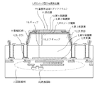
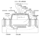
図8に従来の2次元ボロメータ型THz波検出器の画素構造を示す。ボロメータ型THz波検出器20は、読出回路2a等が形成された回路基板2上に、入射するTHz波を反射する反射膜3と読出回路2aに接続するためのコンタクト4が形成され、その上に第1保護膜5が形成されている。また、コンタクト4上に、第2保護膜6、第3保護膜8、電極配線9、第4保護膜10からなる支持部13が形成され、コンタクト4を介して読出回路2aと電極配線9とが接続されている。また、この支持部13によって、第2保護膜6、ボロメータ薄膜7、第3保護膜8、第4保護膜10、吸収膜11からなる温度検出部(ダイアフラム)14が中空に保持され(エアギャップ15)、ボロメータ薄膜7の両端部には電極配線9が接続されている。
FIG. 8 shows a pixel structure of a conventional two-dimensional bolometer type THz wave detector. In the bolometer type
従来技術の場合、例えば、本願出願人の先願(特願2009−258923号)では、図8(先願の図2に相当)のエアギャップ15を8〜14μmにすることを特徴としている。また、一般的に光学干渉を用いた吸収構造を考えた場合、エアギャップ15を検出したい波長の1/4に設定するのが好ましい。 In the case of the prior art, for example, the prior application (Japanese Patent Application No. 2009-258923) of the applicant of the present application is characterized in that the air gap 15 in FIG. 8 (corresponding to FIG. 2 of the prior application) is 8 to 14 μm. In general, when considering an absorption structure using optical interference, it is preferable to set the air gap 15 to ¼ of the wavelength to be detected.
しかしながら、エアギャップを従来技術の様に広げる検討を行った結果、製造工程の熱処理などの影響で温度検出部14に亀裂が発生し、この部分が欠陥画素となり、製造歩留りを悪化させていることを突き止めた。 However, as a result of studying to widen the air gap as in the prior art, cracks are generated in the temperature detection unit 14 due to the influence of heat treatment in the manufacturing process, and this portion becomes a defective pixel, which deteriorates the manufacturing yield. I found out.
前述の温度検出部14の亀裂は、犠牲層(製造工程途中で温度検出部14を保持するもので、最終的に除去されるため、図8には示していない。)に用いる材質と温度検出部14を主に構成する第2保護膜6、第3保護膜8及び第4保護膜10との熱膨張係数差に依存し、図9に示すように、犠牲層を厚く(エアギャップを大きく)すると、亀裂の発生頻度が高く(欠陥画素数が多く)なる。 The cracks in the temperature detection unit 14 described above are used for the sacrificial layer (which is not shown in FIG. 8 because it holds the temperature detection unit 14 in the middle of the manufacturing process and is eventually removed). As shown in FIG. 9, the sacrificial layer is thickened (the air gap is increased), depending on the difference in thermal expansion coefficient between the second protective film 6, the third protective film 8 and the fourth protective film 10 mainly constituting the portion 14. ), The frequency of occurrence of cracks is high (the number of defective pixels is large).
本発明は、このような問題点に鑑みてなされたものであって、主たる目的は、高い製造歩留りで作成することができる高感度ボロメータ型THz波検出器を提供することにある。 The present invention has been made in view of such problems, and a main object thereof is to provide a high-sensitivity bolometer-type THz wave detector that can be produced with a high production yield.
上記目的を達成するために、本発明は、基板に形成された読出回路に接続される電気配線を含む支持部により、前記電気配線に接続されるボロメータ薄膜を含む温度検出部が、前記基板から浮いた状態で支持される熱分離構造を有するボロメータ型THz波検出器であって、前記基板上の前記温度検出部に対向する位置にTHz波を反射する反射膜が形成され、前記温度検出部の表面、裏面あるいは内部に前記THz波を吸収する吸収膜が形成され、前記反射膜と前記温度検出部とで光学的共振構造が形成され、前記反射膜上にTHz波に対して透明な誘電体が形成され、前記誘電体の上面と前記温度検出部の下面との間隔が8μm未満となるように、前記誘電体の膜厚が設定されていることを特徴とする。 In order to achieve the above object, according to the present invention, a temperature detection unit including a bolometer thin film connected to the electrical wiring is provided from the substrate by a support unit including electrical wiring connected to a readout circuit formed on the substrate. A bolometer type THz wave detector having a thermal separation structure supported in a floating state, wherein a reflective film for reflecting THz waves is formed on the substrate at a position facing the temperature detection unit, and the temperature detection unit An absorption film that absorbs the THz wave is formed on the front surface, the back surface, or the inside, and an optical resonance structure is formed by the reflection film and the temperature detection unit, and a dielectric that is transparent to the THz wave is formed on the reflection film. A dielectric is formed, and the film thickness of the dielectric is set so that the distance between the upper surface of the dielectric and the lower surface of the temperature detection unit is less than 8 μm.
本発明のボロメータ型THz波検出器によれば、エアギャップ(温度検出部を中空に浮かせる間隔)を小さく(好ましくは8μm未満)する代わりに、反射膜上の誘電体を厚くするため、ギャップ(光学的共振構造を形成する間隔)を適切に設定することによって、THz波帯の電磁波を効率的に吸収させることが可能となる。また、エアギャップを小さくすることによって、製造上の課題である温度検出部14の亀裂を抑制することができ、THz波検出器を高い歩留まりで製造することができる。 According to the bolometer-type THz wave detector of the present invention, in order to increase the thickness of the dielectric on the reflective film, instead of reducing the air gap (the interval at which the temperature detecting unit is floated in the air) (preferably less than 8 μm), the gap ( By appropriately setting the interval at which the optical resonant structure is formed, it is possible to efficiently absorb electromagnetic waves in the THz wave band. In addition, by reducing the air gap, it is possible to suppress cracking of the temperature detection unit 14 that is a manufacturing problem, and it is possible to manufacture a THz wave detector with a high yield.
なお、詳細は示していないが、製造工程中に用いる犠牲層の材料と温度検出部に用いる材料との熱膨張係数差によっては、エアギャップの上限が変化することは述べるまでもない。 Although not shown in detail, it goes without saying that the upper limit of the air gap varies depending on the difference in thermal expansion coefficient between the material of the sacrificial layer used during the manufacturing process and the material used for the temperature detection unit.
背景技術で示したように、ボロメータ型THz波検出器において、光学干渉を用いた吸収構造を考えた場合、エアギャップを検出したい波長の1/4に設定するのが好ましく、例えば、8〜14μmに設定しているが、エアギャップを大きくすると、製造工程の熱処理などの影響で温度検出部に亀裂が発生して欠陥画素が生じ、製造歩留りを悪化させるという問題が生じる。 As shown in the background art, when an absorption structure using optical interference is considered in the bolometer type THz wave detector, it is preferable to set the air gap to ¼ of the wavelength to be detected, for example, 8 to 14 μm. However, when the air gap is increased, a crack occurs in the temperature detection part due to the influence of heat treatment in the manufacturing process, and defective pixels are generated, resulting in a problem that the manufacturing yield is deteriorated.
そこで、本発明の一実施の形態では、基板に形成された読出回路に接続される電気配線を含む支持部により、電気配線に接続されるボロメータ薄膜を含む温度検出部が、基板から浮いた状態で支持される熱分離構造を有し、基板上の温度検出部に対向する位置にTHz波を反射する反射膜が形成され、温度検出部の表面、裏面あるいは内部にTHz波を吸収する吸収膜が形成され、反射膜と吸収膜とで光学的共振構造が形成され、反射膜上にTHz波に対して透明な誘電体が形成されている構造において、誘電体の上面と温度検出部の下面との間隔が、8μm未満となるように、誘電体の膜厚を設定する。 Therefore, in one embodiment of the present invention, the temperature detection unit including the bolometer thin film connected to the electrical wiring is floated from the substrate by the support unit including the electrical wiring connected to the readout circuit formed on the substrate. A reflective film that reflects the THz wave at a position facing the temperature detection unit on the substrate, and absorbs the THz wave on the front, back, or inside of the temperature detection unit In the structure in which an optical resonance structure is formed by the reflection film and the absorption film, and a dielectric transparent to the THz wave is formed on the reflection film, the upper surface of the dielectric and the lower surface of the temperature detection unit The film thickness of the dielectric is set so that the distance between and is less than 8 μm.
これにより、従来の構造に比べて、エアギャップを小さくすることができるため、熱処理などを起因とする欠陥画素の発生を抑制し、製造歩留りを向上させることができる。 As a result, the air gap can be reduced as compared with the conventional structure, so that the generation of defective pixels due to heat treatment or the like can be suppressed, and the manufacturing yield can be improved.
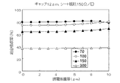
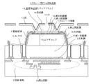
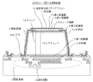
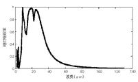
上記実施形態について更に詳細に説明すべく、本発明の第1の実施例に係るボロメータ型THz波検出器について、図1、図2及び図10を参照に説明する。図1は、本実施例のボロメータ型THz波検出器の画素構造を示す図であり、図2は、ギャップを12μmとした場合の、誘電体膜厚と吸収率との関係を示す図である。また、図10は、窒化ケイ素の吸収特性を示す図である。 In order to describe the above embodiment in more detail, a bolometer type THz wave detector according to a first example of the present invention will be described with reference to FIG. 1, FIG. 2, and FIG. FIG. 1 is a diagram showing a pixel structure of a bolometer type THz wave detector of the present embodiment, and FIG. 2 is a diagram showing a relationship between a dielectric film thickness and an absorptance when a gap is set to 12 μm. . FIG. 10 is a diagram showing the absorption characteristics of silicon nitride.
図1に示すように、本実施例のボロメータ型THz波検出器1は、読出回路2a等が形成された回路基板2上に、入射するTHz波を反射する反射膜3と読出回路2aに接続するためのコンタクト4が形成され、その上に第1保護膜5が形成されている。また、コンタクト4上に、第2保護膜6、第3保護膜8、電極配線9、第4保護膜10からなる支持部13が形成され、コンタクト4を介して読出回路2aと電極配線9とが接続されている。また、この支持部13によって、第2保護膜6、ボロメータ薄膜7、第3保護膜8、第4保護膜10、吸収膜11からなる温度検出部14(ダイアフラム)が中空に保持され、ボロメータ薄膜7の両端部は電極配線9が接続されている。
As shown in FIG. 1, the bolometer type THz wave detector 1 of this embodiment is connected to a reflection film 3 for reflecting an incident THz wave on a
ここで、上述したように、THz波を効率的に吸収するためには、光学的共振構造の条件(吸収膜11と反射膜3の間隔、すなわちギャップ16)を適切に設定する必要があるが、エアギャップを大きくすると、製造工程の熱処理などの影響で温度検出部に亀裂が発生して欠陥画素が生じ、製造歩留りを悪化させるという問題が生じる。そこで、本実施例では、ギャップ16をTHz波を効率的に吸収可能な値に設定しつつ、エアギャップ15を小さくできるようにするために、第1保護膜5を厚くする。 Here, as described above, in order to efficiently absorb the THz wave, it is necessary to appropriately set the conditions of the optical resonance structure (the distance between the absorption film 11 and the reflection film 3, that is, the gap 16). If the air gap is increased, a crack is generated in the temperature detection portion due to the heat treatment in the manufacturing process, and defective pixels are generated, resulting in a problem that the manufacturing yield is deteriorated. Therefore, in the present embodiment, the first protective film 5 is thickened so that the air gap 15 can be reduced while the gap 16 is set to a value capable of efficiently absorbing the THz wave.
図2は、吸収膜11のシート抵抗を150Ω/□、ギャップ16を12μmとし、誘電体膜厚(図1では第1保護膜5の膜厚)を0から10μmとした場合の、総合吸収率の計算結果例を示す。計算例は波長70、100、150、300μmとし、誘電体の屈折率を2としている。誘電体膜厚0μmは、図8に示す従来例でエアギャップ15を12μmとした場合と同じである。 FIG. 2 shows the total absorption rate when the sheet resistance of the absorption film 11 is 150Ω / □, the gap 16 is 12 μm, and the dielectric film thickness (the film thickness of the first protective film 5 in FIG. 1) is 0 to 10 μm. An example of the calculation result is shown. In the calculation example, the wavelengths are 70, 100, 150, and 300 μm, and the refractive index of the dielectric is 2. The dielectric film thickness of 0 μm is the same as when the air gap 15 is 12 μm in the conventional example shown in FIG.
図2から明らかなように、誘電体膜厚を厚くすることにより、吸収率は改善傾向にある。計算例では、波長及び誘電体膜厚にもよるが、従来例に比べ最大で7%吸収率が改善している。このシート抵抗ならびにギャップ16、誘電体膜厚(図1では第1保護膜5の膜厚)はそれぞれ計算により適切な値を求めることができる。 As is clear from FIG. 2, the absorption rate tends to be improved by increasing the dielectric film thickness. In the calculation example, although it depends on the wavelength and the dielectric film thickness, the absorption rate is improved by 7% at the maximum compared to the conventional example. The sheet resistance, the gap 16, and the dielectric film thickness (the film thickness of the first protective film 5 in FIG. 1) can be determined appropriately by calculation.
なお、窒化ケイ素の吸収率については、Q.Hu等の講演資料(”Real-time THz Imaging Using Quantum-cascade Lasers and Focal-plane Array Cameras”, 2nd International Workshop on Quantum Cascade Lasers, September 6-9 (2006))に記載されており、それを図10に示す。同図を見て分かるように、窒化ケイ素は、波長50μm以上でほぼ透明になる。したがって、第1保護膜5を窒化ケイ素で形成する場合は、波長50μm以下の領域においては、第1保護膜5により入射エネルギーが吸収されるため、著しく感度が低下することを念頭に置く必要がある。 Regarding the absorption rate of silicon nitride, Q. Hu et al. (“Real-time THz Imaging Using Quantum-cascade Lasers and Focal-plane Array Cameras”, 2nd International Workshop on Quantum Cascade Lasers, September 6-9 ( 2006)) and is shown in FIG. As can be seen from the figure, silicon nitride becomes almost transparent at a wavelength of 50 μm or more. Therefore, in the case where the first protective film 5 is formed of silicon nitride, it is necessary to keep in mind that the sensitivity is significantly lowered because incident energy is absorbed by the first protective film 5 in a region of a wavelength of 50 μm or less. is there.
以上より、エアギャップ15を設定する際には、図2の総合吸収率と、誘電体(第1保護膜5)自身の吸収と、エアギャップ15を大きくすることによる歩留まりの低下と、を総合的に勘案する必要があり、図9の欠陥画素数はエアギャップが8μm以上で急激に増加していることから、エアギャップ15は、8μm未満(より好ましくは7μm以下)が適切であると言える。 From the above, when setting the air gap 15, the total absorption rate of FIG. 2, the absorption of the dielectric (first protective film 5) itself, and the decrease in yield due to the increase in the air gap 15 are combined. In view of the fact that the number of defective pixels in FIG. 9 increases rapidly when the air gap is 8 μm or more, it can be said that the air gap 15 is suitably less than 8 μm (more preferably 7 μm or less). .
以下、上記構造のボロメータ型THz波検出器1の製造方法の一例について概説する。 Hereinafter, an example of a manufacturing method of the bolometer type THz wave detector 1 having the above structure will be outlined.
まず、CMOS回路等の読出回路2aを形成した回路基板2上に、スパッタ法によりAl、Ti等の金属を成膜し、レジストをマスクとしてパターン形成を行い、各画素の温度検出部14に入射するTHz波を反射するための反射膜3及び電極配線9と読出回路2aとを接続するためのコンタクト4を形成する。なお、上記金属はTHz波の反射率が高く、電気抵抗が小さい材料であればよく、Al、Tiに限定されない。
First, a metal such as Al or Ti is formed on a
次に、回路基板2全面に、プラズマCVD法によりシリコン酸化膜(SiO、SiO2)、シリコン窒化膜(SiN、Si3N4)、シリコン酸窒化膜(SiON)などを成膜し、反射膜3及びコンタクト4を保護する第1保護膜5を形成する。この第1保護膜5の膜厚は、ギャップ16(反射膜3と吸収膜11の間隔)がTHz波を効率的に吸収できる値となり、かつ、エアギャップ15(温度検出部14を中空に浮かせる間隔、すなわち、第1保護膜5の上面と温度検出部14の下面との間隔)が8μm未満となるように設定する。
Next, a silicon oxide film (SiO, SiO 2 ), a silicon nitride film (SiN, Si 3 N 4 ), a silicon oxynitride film (SiON), etc. are formed on the entire surface of the
次に、回路基板2全面に感光性ポリイミド膜等の有機膜を塗布し、コンタクト4及び画素間の領域が露出するように露光・現像を行った後、400℃程度の温度で焼締めを行い、マイクロブリッジ構造を形成するための犠牲層を形成する。その際、キュア後の感光性ポリイミド膜は、エアギャップ15が8μm未満となるような厚さに設定する。
Next, an organic film such as a photosensitive polyimide film is applied to the entire surface of the
次に、犠牲層の上に、プラズマCVD法によりシリコン酸化膜(SiO、SiO2)、シリコン窒化膜(SiN、Si3N4)、シリコン酸窒化膜(SiON)などを成膜し、第2保護膜6を形成する。 Next, a silicon oxide film (SiO, SiO 2 ), a silicon nitride film (SiN, Si 3 N 4 ), a silicon oxynitride film (SiON), or the like is formed on the sacrificial layer by a plasma CVD method. A protective film 6 is formed.
次に、第2保護膜6の上に、酸素雰囲気の反応性スパッタにより酸化バナジウム(V2O3、VOXなど)や酸化チタン(TiOX)などを堆積し、レジストをマスクとしてパターン形成を行い、温度検出部14となる部分にボロメータ薄膜7を形成する。なお、ここではボロメータ薄膜7として酸化バナジウムや酸化チタンを用いているが、抵抗温度係数(TCR:Temperature Coefficient Resistance)の大きい他の材料を用いることもできる。 Then, on the second protective layer 6 and the deposited vanadium oxide by a reactive sputtering an oxygen atmosphere (V 2 O 3, VO X, etc.) or titanium oxide (TiO X), the patterned resist as a mask Then, the bolometer thin film 7 is formed in a portion that becomes the temperature detection unit 14. Here, vanadium oxide or titanium oxide is used as the bolometer thin film 7, but other materials having a high temperature coefficient coefficient (TCR) can also be used.
次に、プラズマCVD法によりシリコン酸化膜(SiO,SiO2)、シリコン窒化膜(SiN,Si3N4)、シリコン酸窒化膜(SiON)などを成膜し、ボロメータ薄膜7を保護する第3保護膜8を形成する。その後、コンタクト4上の第1保護膜5、第2保護膜6及び第3保護膜8、ボロメータ薄膜7端部の第3保護膜8を除去する。
Next, a silicon oxide film (SiO, SiO 2 ), a silicon nitride film (SiN, Si 3 N 4 ), a silicon oxynitride film (SiON), or the like is formed by plasma CVD to protect the bolometer thin film 7 in a third manner. A protective film 8 is formed. Thereafter, the first protective film 5, the second protective film 6, the third protective film 8, and the third protective film 8 at the end of the bolometer thin film 7 on the
次に、スパッタ法によりAl、Cu、Au、Ti、W、Moなどの金属を成膜した後、レジストをマスクとしてパターン形成を行い、電極配線9を形成する。この電極配線9はコンタクト4を介してボロメータ薄膜7と回路基板2内の読出回路2aとを電気的に接続すると共に、ボロメータ薄膜7を中空に保持する支持部13としての役割を果たす。
Next, after depositing a metal such as Al, Cu, Au, Ti, W, or Mo by sputtering, pattern formation is performed using a resist as a mask to form the electrode wiring 9. The electrode wiring 9 serves as a support portion 13 for electrically connecting the bolometer thin film 7 and the readout circuit 2a in the
その後、プラズマCVD法によりシリコン酸化膜(SiO,SiO2)、シリコン窒化膜(SiN,Si3N4)、シリコン酸窒化膜(SiON)などを成膜し、電極配線9を保護する第4保護膜10を形成する。 Thereafter, a silicon oxide film (SiO, SiO 2 ), a silicon nitride film (SiN, Si 3 N 4 ), a silicon oxynitride film (SiON), or the like is formed by plasma CVD, and a fourth protection for protecting the electrode wiring 9 A film 10 is formed.
次に、スパッタ法によりAl、Tiなどの金属を成膜した後、レジストをマスクとしてパターン形成を行い、吸収膜11を形成する。その際、第2保護膜6、第3保護膜8、ボロメータ薄膜7、第4保護膜10、吸収膜11を合わせた温度検出部14のシート抵抗が適切な値になるように膜厚を設定する。この吸収膜11はTHz波を効率的に吸収する役割を果たす。なお、上記金属は温度検出部14のシート抵抗を適切な値に設定可能な材料であればよく、Al、Tiに限定されない。また、図1では、吸収膜11を温度検出部14の表面に形成しているが、吸収膜11は反射膜3と対向するように配置されていればよく、温度検出部14の表面、裏面あるいは内部のいずれに形成してもよい。 Next, after depositing a metal such as Al or Ti by sputtering, pattern formation is performed using a resist as a mask to form the absorption film 11. At that time, the film thickness is set so that the sheet resistance of the temperature detection unit 14 including the second protective film 6, the third protective film 8, the bolometer thin film 7, the fourth protective film 10, and the absorption film 11 becomes an appropriate value. To do. The absorption film 11 plays a role of efficiently absorbing THz waves. In addition, the said metal should just be a material which can set the sheet resistance of the temperature detection part 14 to an appropriate value, and is not limited to Al and Ti. In FIG. 1, the absorption film 11 is formed on the surface of the temperature detection unit 14, but the absorption film 11 may be disposed so as to face the reflection film 3. Or you may form in any inside.
その後、一フッ化メタンと酸素の混合ガスを用いたプラズマエッチングにより、第2保護膜6と第3保護膜8と第4保護膜10とを部分的にエッチングして、犠牲層上の所定の領域にスルーホールを形成してポリイミドを部分的に露出させ、O2ガスプラズマを用いたアッシングにより犠牲層を除去し、温度検出部14が支持部13によって回路基板2から浮いたマイクロブリッジ構造のボロメータ型THz検出器1が完成する。
Thereafter, the second protective film 6, the third protective film 8, and the fourth protective film 10 are partially etched by plasma etching using a mixed gas of monofluoromethane and oxygen to form a predetermined layer on the sacrificial layer. Through-holes are formed in the region to partially expose the polyimide, the sacrificial layer is removed by ashing using O 2 gas plasma, and the temperature detecting unit 14 is lifted from the
なお、上記製造方法では、第1保護膜5、第2保護膜6、ボロメータ薄膜7及び第3保護膜8を形成した後、コンタクト4上の第1保護膜5、第2保護膜6及び第3保護膜8を除去する構成としたが、例えば、第1保護膜5を形成した後にコンタクト4上の第1保護膜5を除去し、除去した部分にCMP法などを用いて金属を埋設してビアを形成し、その後、第2保護膜6、ボロメータ薄膜7及び第3保護膜8を形成し、ビア上の第2保護膜6及び第3保護膜8を除去する構成とすることもできる。
In the above manufacturing method, after the first protective film 5, the second protective film 6, the bolometer thin film 7 and the third protective film 8 are formed, the first protective film 5, the second protective film 6 and the second protective film 6 on the
また、犠牲層をポリシリコンやAlで構成することもできる。ポリシリコンを用いる場合は、例えば、ヒドラジンやテトラメチルアンモニウムハイドロオキサイド(TMAH)を用いたウェットエッチング、XeF2プラズマを用いたドライエッチング等により犠牲層を除去することができる。また、Alを用いる場合は、例えば、塩酸やホットリン酸を用いたウェットエッチングにより犠牲層を除去することができる。 The sacrificial layer can also be made of polysilicon or Al. When polysilicon is used, the sacrificial layer can be removed by wet etching using hydrazine or tetramethylammonium hydroxide (TMAH), dry etching using XeF 2 plasma, or the like. When Al is used, the sacrificial layer can be removed by wet etching using hydrochloric acid or hot phosphoric acid, for example.
また、第2保護膜6、第3保護膜8、第4保護膜10にシリコン酸化膜を用いる場合には、犠牲層をシリコン窒化膜で構成することも可能であり、さらに、その逆も可能である。シリコン窒化膜を犠牲層とする場合は、例えば、ホットリン酸を用いたウェットエッチングで除去することができ、シリコン酸化膜を犠牲層とする場合は、例えば、弗酸を用いたウェットエッチングで除去することができる。 Further, when a silicon oxide film is used for the second protective film 6, the third protective film 8, and the fourth protective film 10, the sacrificial layer can be formed of a silicon nitride film, and vice versa. It is. When the silicon nitride film is used as a sacrificial layer, for example, it can be removed by wet etching using hot phosphoric acid, and when the silicon oxide film is used as a sacrificial layer, for example, it is removed by wet etching using hydrofluoric acid. be able to.
このように、本実施例では、反射膜3と吸収膜11の間隔(ギャップ16)は変えずに、第1保護膜5の上面と温度検出部14の下面との間隔(エアギャップ15)が8μm未満となるように第1保護膜5の膜厚を設定することにより、高性能なボロメータ型THz波検出器1を歩留まりよく製造することができる。 Thus, in this embodiment, the distance (air gap 15) between the upper surface of the first protective film 5 and the lower surface of the temperature detector 14 is not changed without changing the distance (gap 16) between the reflective film 3 and the absorption film 11. By setting the film thickness of the first protective film 5 to be less than 8 μm, the high-performance bolometer type THz wave detector 1 can be manufactured with high yield.
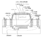
次に、本発明の第2の実施例に係るボロメータ型THz波検出器について、図3を参照に説明する。図3は、本実施例に係るボロメータ型THz波検出器の画素構造を示す図である。 Next, a bolometer type THz wave detector according to a second embodiment of the present invention will be described with reference to FIG. FIG. 3 is a diagram illustrating a pixel structure of the bolometer type THz wave detector according to the present embodiment.
前記した第1の実施例は、温度検出部14のみでTHz波を受光する構造であるが、本実施例では、受光面積を広げるため、温度検出部14の周囲から隣接する画素に延びる庇を追加する。図3は、本実施例のボロメータ型THz波検出器1の画像構造を示しており、庇12によって、温度検出部14の周囲に入射するTHz波を吸収することができ、ボロメータ型THz波検出器1の感度を向上させることができる。 In the first embodiment described above, the THz wave is received only by the temperature detection unit 14, but in this embodiment, in order to increase the light receiving area, a ridge extending from the periphery of the temperature detection unit 14 to adjacent pixels is provided. to add. FIG. 3 shows an image structure of the bolometer type THz wave detector 1 of the present embodiment. The THz wave incident on the periphery of the temperature detection unit 14 can be absorbed by the ridge 12, and the bolometer type THz wave detection is performed. The sensitivity of the device 1 can be improved.
以下、上記構造のボロメータ型THz波検出器1の製造方法の一例について概説する。 Hereinafter, an example of a manufacturing method of the bolometer type THz wave detector 1 having the above structure will be outlined.
まず、前記した第1の実施例と同様に、CMOS回路等の読出回路2aを形成した回路基板2上に、反射膜3及びコンタクト4を形成し、その上に第1保護膜5を形成した後、温度検出部14となる領域に犠牲層を形成する。次に、犠牲層の上に第2保護膜6、ボロメータ薄膜7、第3保護膜8を形成し、コンタクト4上の第1保護膜5、第2保護膜6及び第3保護膜8、ボロメータ薄膜7端部の第3保護膜8を除去する。次に、電極配線9、第4保護膜10を形成する。なお、第1保護膜5の膜厚は、ギャップ16(反射膜3と吸収膜11の間隔)がTHz波を効率的に吸収できる値となり、かつ、エアギャップ15(温度検出部14を中空に浮かせる間隔、すなわち、第1保護膜5の上面と温度検出部14の下面との間隔)が8μm未満となるように設定する。
First, as in the first embodiment, the reflective film 3 and the
次に、本実施例では、一フッ化メタンと酸素の混合ガスを用いたプラズマエッチングにより、第2保護膜6と第3保護膜8と第4保護膜10とを部分的にエッチングして、犠牲層上の所定の領域にスルーホールを形成し、ポリイミドを部分的に露出させる。 Next, in this embodiment, the second protective film 6, the third protective film 8, and the fourth protective film 10 are partially etched by plasma etching using a mixed gas of methane monofluoride and oxygen, A through hole is formed in a predetermined region on the sacrificial layer, and the polyimide is partially exposed.
次に、回路基板2全面に感光性ポリイミドを塗布し、温度検出部14の周縁部が露出するように露光・現像を行った後、熱処理を施して、温度検出部14の中央部及び隣接する温度検出部14の間の領域に第2犠牲層を形成する。第2犠牲層の厚さは、例えば、0.5〜3μm程度である。
Next, photosensitive polyimide is applied to the entire surface of the
次に、シリコン酸化膜(SiO、SiO2)、シリコン窒化膜(SiN,Si3N4)、シリコン酸窒化膜(SiON)などの絶縁材料を形成した後、温度検出部14中央部の上記絶縁材料を除去して庇12を形成する。 Next, after forming an insulating material such as a silicon oxide film (SiO, SiO 2 ), a silicon nitride film (SiN, Si 3 N 4 ), or a silicon oxynitride film (SiON), the insulation at the center of the temperature detection unit 14 is performed. The material is removed to form the ridges 12.
次に、スパッタ法によりAl、Tiなどの金属を成膜した後、レジストをマスクとしてパターン形成を行い、温度検出部14中央部及び庇12上に吸収膜11を形成する。その際、第1の実施例と同様に、第2保護膜6、第3保護膜8、ボロメータ薄膜7、第4保護膜10、吸収膜11、庇12を合わせた温度検出部14のシート抵抗が適切な値となるように膜厚を設定する。なお、図3では、吸収膜11を温度検出部14及び庇12の表面に形成しているが、吸収膜11は反射膜3と対向するように配置されていればよく、温度検出部14及び庇12の表面、裏面あるいは内部のいずれに形成してもよい。 Next, after depositing a metal such as Al or Ti by sputtering, pattern formation is performed using the resist as a mask, and the absorption film 11 is formed on the central portion of the temperature detection unit 14 and the ridge 12. At that time, as in the first embodiment, the sheet resistance of the temperature detector 14 including the second protective film 6, the third protective film 8, the bolometer thin film 7, the fourth protective film 10, the absorption film 11, and the ridge 12 is combined. The film thickness is set so that becomes an appropriate value. In FIG. 3, the absorption film 11 is formed on the surface of the temperature detection unit 14 and the flange 12. However, the absorption film 11 may be disposed so as to face the reflection film 3. You may form in any of the surface, the back surface, or the inside of the collar 12.
その後、隣接する画素間の庇12にスルーホールを形成してポリイミドを部分的に露出させ、O2ガスプラズマを用いたアッシングにより犠牲層及び第2犠牲層を除去し、温度検出部14が支持部13によって回路基板2から浮いたマイクロブリッジ構造のボロメータ型THz検出器1が完成する。
Thereafter, through holes are formed in the ridges 12 between adjacent pixels to partially expose the polyimide, the sacrificial layer and the second sacrificial layer are removed by ashing using O 2 gas plasma, and the temperature detection unit 14 supports The micro bridge structure bolometer type THz detector 1 floating from the
このように、本実施例でも、反射膜3と吸収膜11の間隔(ギャップ16)は変えずに、第1保護膜5の上面と温度検出部14の下面との間隔(エアギャップ15)が8μm未満となるように第1保護膜5の膜厚を設定することにより、高性能なボロメータ型THz波検出器1を歩留まりよく製造することができる。 Thus, also in the present embodiment, the distance (air gap 15) between the upper surface of the first protective film 5 and the lower surface of the temperature detector 14 is not changed without changing the distance (gap 16) between the reflective film 3 and the absorption film 11. By setting the film thickness of the first protective film 5 to be less than 8 μm, the high-performance bolometer type THz wave detector 1 can be manufactured with high yield.
次に、本発明の第3の実施例に係るボロメータ型THz波検出器について、図4を参照に説明する。図4は、本実施例に係るボロメータ型THz波検出器の画素構造を示す図である。 Next, a bolometer type THz wave detector according to a third embodiment of the present invention will be described with reference to FIG. FIG. 4 is a diagram illustrating a pixel structure of the bolometer type THz wave detector according to the present embodiment.
前記した第2の実施例では、温度検出部14の下部と庇12の下部とでギャップが異なるため、干渉効果が若干阻害される。そこで、本実施例では、これを改善するために、図4に示すように、ギャップ16が画素内でほぼ同じとなるようする。 In the second embodiment described above, since the gap is different between the lower part of the temperature detection unit 14 and the lower part of the ridge 12, the interference effect is slightly inhibited. Therefore, in this embodiment, in order to improve this, as shown in FIG. 4, the gap 16 is made substantially the same in the pixel.
以下、上記構造のボロメータ型THz波検出器1の製造方法の一例について概説する。 Hereinafter, an example of a manufacturing method of the bolometer type THz wave detector 1 having the above structure will be outlined.
まず、第1の実施例と同様に、CMOS回路等の読出回路2aを形成した回路基板2上に、反射膜3及びコンタクト4を形成し、その上に第1保護膜5を形成した後、温度検出部14となる領域に犠牲層を形成する。次に、犠牲層の上に第2保護膜6、ボロメータ薄膜7、第3保護膜8を形成し、コンタクト4上の第1保護膜5、第2保護膜6及び第3保護膜8、ボロメータ薄膜7端部の第3保護膜8を除去する。次に、電極配線9、第4保護膜10を形成する。なお、第1保護膜5の膜厚は、ギャップ16(反射膜3と吸収膜11の間隔)がTHz波を効率的に吸収できる値となり、かつ、エアギャップ15(温度検出部14を中空に浮かせる間隔、すなわち、第1保護膜5の上面と温度検出部14の下面との間隔)が8μm未満となるように設定する。
First, as in the first embodiment, after the reflective film 3 and the
次に、第2の実施例と同様に、第2保護膜6と第3保護膜8と第4保護膜10とを部分的にエッチングしてスルーホールを形成し、ポリイミドを部分的に露出させる。次に、回路基板2全面に感光性ポリイミドを塗布し、温度検出部14の周縁部が露出するように露光・現像を行った後、熱処理を施して第2犠牲層を形成する。
Next, as in the second embodiment, the second protective film 6, the third protective film 8, and the fourth protective film 10 are partially etched to form through holes, and the polyimide is partially exposed. . Next, photosensitive polyimide is applied to the entire surface of the
次に、シリコン酸化膜(SiO、SiO2)、シリコン窒化膜(SiN,Si3N4)、シリコン酸窒化膜(SiON)などの絶縁材料を形成した後、本実施例では、温度検出部14中央の穴17に相当する部分の上記絶縁材料を除去して庇12を形成する。 Next, after forming an insulating material such as a silicon oxide film (SiO, SiO 2 ), a silicon nitride film (SiN, Si 3 N 4 ), or a silicon oxynitride film (SiON), in this embodiment, the temperature detection unit 14 is used. A portion of the insulating material corresponding to the central hole 17 is removed to form the ridge 12.
次に、スパッタ法によりAl、Tiなどの金属を成膜した後、レジストをマスクとしてパターン形成を行い、庇12上に吸収膜11を形成する。その後、隣接する画素間の庇12にスルーホールを形成してポリイミドを部分的に露出させ、O2ガスプラズマを用いたアッシングにより犠牲層及び第2犠牲層を除去し、温度検出部14が支持部13によって回路基板2から浮いたマイクロブリッジ構造のボロメータ型THz検出器1が完成する。なお、図4では、吸収膜11を温度検出部14及び庇12の表面に形成しているが、吸収膜11は反射膜3と対向するように配置されていればよく、温度検出部14及び庇12の表面、裏面あるいは内部のいずれに形成してもよい。
Next, after depositing a metal such as Al or Ti by sputtering, pattern formation is performed using a resist as a mask, and the absorption film 11 is formed on the ridge 12. Thereafter, through holes are formed in the ridges 12 between adjacent pixels to partially expose the polyimide, the sacrificial layer and the second sacrificial layer are removed by ashing using O 2 gas plasma, and the temperature detection unit 14 supports The micro bridge structure bolometer type THz detector 1 floating from the
このように、本実施例でも、反射膜3と吸収膜11の間隔(ギャップ16)は変えずに、第1保護膜5の上面と温度検出部14の下面との間隔(エアギャップ15)が8μm未満となるように第1保護膜5の膜厚を設定することにより、高性能なボロメータ型THz波検出器1を歩留まりよく製造することができる。 Thus, also in the present embodiment, the distance (air gap 15) between the upper surface of the first protective film 5 and the lower surface of the temperature detector 14 is not changed without changing the distance (gap 16) between the reflective film 3 and the absorption film 11. By setting the film thickness of the first protective film 5 to be less than 8 μm, the high-performance bolometer type THz wave detector 1 can be manufactured with high yield.
次に、本発明の第4の実施例に係るボロメータ型THz波検出器について、図5を参照に説明する。図5は、本実施例に係るボロメータ型THz波検出器の画素構造を示す図である。 Next, a bolometer type THz wave detector according to a fourth embodiment of the present invention will be described with reference to FIG. FIG. 5 is a diagram illustrating a pixel structure of the bolometer type THz wave detector according to the present embodiment.
前記した第1の実施例において、エアギャップ15を8μm未満とする代わりに、誘電体(第1保護膜5)の膜厚を厚くしたが、第1保護膜5を厚くするとコンタクト4が深くなり、電極配線9の断線が生じやすくなる。そこで、本実施例では、これを改善するために、半導体製造工程における配線形成手法を利用して、図5に示すように、反射膜3として利用する配線の上に、ビアと配線層を順次積層し、電極配線9を読出回路2aに接続するための多層配線構造を形成する。これにより、高性能なボロメータ型THz波検出器1を歩留まりよく製造することができると共に、電極配線9の断線を抑制することができる。なお、この構造は、近年の半導体製造工程で十分実現可能な構造である。
In the first embodiment described above, the thickness of the dielectric (first protective film 5) is increased instead of making the air gap 15 less than 8 μm. However, if the first protective film 5 is increased, the
次に、本発明の第5の実施例に係るボロメータ型THz波検出器について、図6を参照に説明する。図6は、本実施例に係るボロメータ型THz波検出器の画素構造を示す図であり、第2の実施例と第4の実施例のコンタクト形成方法を組み合わせた例である。この構造でも、第4の実施例と同様に、高性能なボロメータ型THz波検出器1を歩留まりよく製造することができると共に、電極配線9の断線を抑制することができる。 Next, a bolometer type THz wave detector according to a fifth example of the present invention will be described with reference to FIG. FIG. 6 is a diagram showing a pixel structure of the bolometer type THz wave detector according to the present embodiment, and is an example in which the contact formation methods of the second embodiment and the fourth embodiment are combined. Even with this structure, as in the fourth embodiment, the high-performance bolometer-type THz wave detector 1 can be manufactured with high yield, and disconnection of the electrode wiring 9 can be suppressed.
次に、本発明の第6の実施例に係るボロメータ型THz波検出器について、図7を参照に説明する。図7は、本実施例に係るボロメータ型THz波検出器の画素構造を示す図であり、第3の実施例と第4の実施例のコンタクト形成方法を組み合わせた例である。この構造でも、第4の実施例と同様に、高性能なボロメータ型THz波検出器1を歩留まりよく製造することができると共に、電極配線9の断線を抑制することができる。 Next, a bolometer type THz wave detector according to a sixth example of the present invention will be described with reference to FIG. FIG. 7 is a diagram showing a pixel structure of the bolometer type THz wave detector according to the present embodiment, and is an example in which the contact formation methods of the third embodiment and the fourth embodiment are combined. Even with this structure, as in the fourth embodiment, the high-performance bolometer-type THz wave detector 1 can be manufactured with high yield, and disconnection of the electrode wiring 9 can be suppressed.
なお、上記各実施例では、温度検出部としてボロメータ薄膜を備えたボロメータ型THz波検出器について述べたが、本発明は上記実施例に限定されるものではなく、光学干渉を用いた吸収構造を備えた任意の検出器に対して、同様に適用することができる。また、上記各実施例では、波長30μm〜1mm程度のTHz波を検出する場合について述べたが、更に長波長の電磁波に対しても適用可能である。 In each of the above embodiments, a bolometer type THz wave detector provided with a bolometer thin film as a temperature detector has been described. However, the present invention is not limited to the above embodiment, and an absorption structure using optical interference is used. The same applies to any detector provided. In each of the above-described embodiments, a case where a THz wave with a wavelength of about 30 μm to 1 mm is detected has been described. However, the present invention can be applied to an electromagnetic wave having a longer wavelength.
本発明は、波長30μm〜1mm程度のTHz波を検出する検出器、特にボロメータ型THz波検出器に利用可能である。 The present invention can be used for a detector for detecting a THz wave having a wavelength of about 30 μm to 1 mm, particularly a bolometer type THz wave detector.
1 ボロメータ型THz波検出器
2 回路基板
2a 読出回路
3 反射膜
4 コンタクト
5 第1保護膜
6 第2保護膜
7 ボロメータ薄膜
8 第3保護膜
9 電極配線
10 第4保護膜
11 吸収膜
12 庇
13 支持部
14 温度検出部(ダイアフラム)
15 エアギャップ
16 ギャップ
17 穴
18 層間絶縁膜
20 従来のボロメータ型THz波検出器
DESCRIPTION OF SYMBOLS 1 Bolometer type
15 Air gap 16 Gap 17 Hole 18
Claims (4)
前記基板上の前記温度検出部に対向する位置にTHz波を反射する反射膜が形成され、前記温度検出部の表面、裏面あるいは内部に前記THz波を吸収する吸収膜が形成され、前記反射膜と前記吸収膜とで光学的共振構造が形成され、
前記反射膜上にTHz波に対して透明な誘電体が形成され、
前記誘電体の上面と前記温度検出部の下面との間隔が8μm未満となるように、前記誘電体の膜厚が設定されていることを特徴とするボロメータ型THz波検出器。 A temperature detection unit including a bolometer thin film connected to the electrical wiring is supported by the support unit including the electrical wiring connected to the readout circuit formed on the substrate in a state of being floated from the substrate. A bolometer type THz wave detector,
A reflective film that reflects THz waves is formed on the substrate at a position facing the temperature detection unit, and an absorption film that absorbs the THz waves is formed on the front, back, or inside of the temperature detection unit, and the reflective film And the absorption film form an optical resonance structure,
A dielectric that is transparent to THz waves is formed on the reflective film,
The bolometer-type THz wave detector, wherein a film thickness of the dielectric is set so that a distance between an upper surface of the dielectric and a lower surface of the temperature detection unit is less than 8 μm.
Priority Applications (2)
| Application Number | Priority Date | Filing Date | Title |
|---|---|---|---|
| JP2011058693A JP2012194080A (en) | 2011-03-17 | 2011-03-17 | Bolometer type thz wave detector |
| US13/422,120 US8541742B2 (en) | 2011-03-17 | 2012-03-16 | Bolometer-type THz wave detector |
Applications Claiming Priority (1)
| Application Number | Priority Date | Filing Date | Title |
|---|---|---|---|
| JP2011058693A JP2012194080A (en) | 2011-03-17 | 2011-03-17 | Bolometer type thz wave detector |
Publications (1)
| Publication Number | Publication Date |
|---|---|
| JP2012194080A true JP2012194080A (en) | 2012-10-11 |
Family
ID=46827730
Family Applications (1)
| Application Number | Title | Priority Date | Filing Date |
|---|---|---|---|
| JP2011058693A Pending JP2012194080A (en) | 2011-03-17 | 2011-03-17 | Bolometer type thz wave detector |
Country Status (2)
| Country | Link |
|---|---|
| US (1) | US8541742B2 (en) |
| JP (1) | JP2012194080A (en) |
Cited By (5)
| Publication number | Priority date | Publication date | Assignee | Title |
|---|---|---|---|---|
| WO2017077996A1 (en) * | 2015-11-04 | 2017-05-11 | 日本電気株式会社 | Bolometer type terahertz wave detector |
| WO2017094280A1 (en) * | 2015-11-30 | 2017-06-08 | 国立大学法人東京大学 | Bolometer-type terahertz wave detection element and bolometer-type terahertz wave detection element array |
| KR20170105534A (en) * | 2015-01-08 | 2017-09-19 | 플리어 시스템즈, 인크. | Apparatus and method for infrared reference pixels |
| KR20210052971A (en) * | 2019-11-01 | 2021-05-11 | 주식회사 트루윈 | Micro bolometer and micro bolometer manufacturing method |
| KR20210114174A (en) * | 2020-03-10 | 2021-09-23 | 한국과학기술원 | A Bolometer MEMS Device And The Manufacturing Method of the Bolometer MEMS Device |
Families Citing this family (11)
| Publication number | Priority date | Publication date | Assignee | Title |
|---|---|---|---|---|
| US9029773B2 (en) * | 2013-02-24 | 2015-05-12 | Vlad Novotny | Sealed infrared imagers |
| CN103193190B (en) * | 2013-04-11 | 2015-07-29 | 电子科技大学 | A kind of infrared-Terahertz two waveband detector array micro-bridge structure and preparation method thereof |
| JP2014235144A (en) * | 2013-06-05 | 2014-12-15 | セイコーエプソン株式会社 | Terahertz wave detecting apparatus, camera, imaging apparatus, and measuring apparatus |
| JP2014235146A (en) * | 2013-06-05 | 2014-12-15 | セイコーエプソン株式会社 | Terahertz wave detecting apparatus, camera, imaging apparatus, and measuring apparatus |
| US9377350B2 (en) * | 2014-09-04 | 2016-06-28 | Newport Fab, Llc | Light sensor with chemically resistant and robust reflector stack |
| CN106115604B (en) * | 2016-07-25 | 2018-09-28 | 电子科技大学 | Terahertz micro-metering bolometer based on metamaterial structure and preparation method thereof |
| EP3522217B1 (en) * | 2016-09-29 | 2021-07-14 | Yantai Raytron Technology Co., Ltd. | Method to prepare pixel for uncooled infrared focal plane detector |
| JP6726087B2 (en) * | 2016-12-14 | 2020-07-22 | 浜松ホトニクス株式会社 | Photo detector |
| US10199424B1 (en) * | 2017-07-19 | 2019-02-05 | Meridian Innovation Pte Ltd | Thermoelectric-based infrared detector having a cavity and a MEMS structure defined by BEOL metals lines |
| FR3081989B1 (en) * | 2018-05-30 | 2020-08-21 | Commissariat Energie Atomique | SENSITIVE PIXEL DETECTION SYSTEM INCLUDING A THERMAL DETECTOR AND A COMPENSATION DEVICE |
| CN109659707B (en) * | 2018-12-24 | 2021-03-09 | 广东工业大学 | Terahertz detector and method based on NxM dielectric resonant antenna array |
Citations (5)
| Publication number | Priority date | Publication date | Assignee | Title |
|---|---|---|---|---|
| JPH11317500A (en) * | 1998-03-04 | 1999-11-16 | Nec Corp | Semiconductor device having capacitive element, and manufacture thereof |
| JP2006324265A (en) * | 2005-05-17 | 2006-11-30 | Matsushita Electric Ind Co Ltd | Semiconductor device |
| JP2008241438A (en) * | 2007-03-27 | 2008-10-09 | Nec Corp | Bolometer type thz wave detector |
| JP2009216558A (en) * | 2008-03-11 | 2009-09-24 | Oki Semiconductor Co Ltd | Manufacturing method of infrared detection element |
| JP2010261935A (en) * | 2009-04-30 | 2010-11-18 | Commissariat A L'energie Atomique & Aux Energies Alternatives | Bolometric detector for detecting electromagnetic radiation in region extending from infrared to terahertz frequencies and array detection device comprising such detectors |
-
2011
- 2011-03-17 JP JP2011058693A patent/JP2012194080A/en active Pending
-
2012
- 2012-03-16 US US13/422,120 patent/US8541742B2/en active Active
Patent Citations (5)
| Publication number | Priority date | Publication date | Assignee | Title |
|---|---|---|---|---|
| JPH11317500A (en) * | 1998-03-04 | 1999-11-16 | Nec Corp | Semiconductor device having capacitive element, and manufacture thereof |
| JP2006324265A (en) * | 2005-05-17 | 2006-11-30 | Matsushita Electric Ind Co Ltd | Semiconductor device |
| JP2008241438A (en) * | 2007-03-27 | 2008-10-09 | Nec Corp | Bolometer type thz wave detector |
| JP2009216558A (en) * | 2008-03-11 | 2009-09-24 | Oki Semiconductor Co Ltd | Manufacturing method of infrared detection element |
| JP2010261935A (en) * | 2009-04-30 | 2010-11-18 | Commissariat A L'energie Atomique & Aux Energies Alternatives | Bolometric detector for detecting electromagnetic radiation in region extending from infrared to terahertz frequencies and array detection device comprising such detectors |
Cited By (13)
| Publication number | Priority date | Publication date | Assignee | Title |
|---|---|---|---|---|
| KR20170105534A (en) * | 2015-01-08 | 2017-09-19 | 플리어 시스템즈, 인크. | Apparatus and method for infrared reference pixels |
| KR102411749B1 (en) | 2015-01-08 | 2022-06-22 | 텔레다인 플리어, 엘엘시 | Apparatus and method for infrared reference pixels |
| WO2017077996A1 (en) * | 2015-11-04 | 2017-05-11 | 日本電気株式会社 | Bolometer type terahertz wave detector |
| JPWO2017077996A1 (en) * | 2015-11-04 | 2018-08-23 | 日本電気株式会社 | Bolometer type terahertz wave detector |
| WO2017094280A1 (en) * | 2015-11-30 | 2017-06-08 | 国立大学法人東京大学 | Bolometer-type terahertz wave detection element and bolometer-type terahertz wave detection element array |
| JPWO2017094280A1 (en) * | 2015-11-30 | 2018-09-13 | 国立大学法人 東京大学 | Bolometer type terahertz wave detecting element and bolometer type terahertz wave detecting element array |
| KR102286307B1 (en) * | 2019-11-01 | 2021-08-05 | 주식회사 트루윈 | Micro bolometer and micro bolometer manufacturing method |
| KR20210052971A (en) * | 2019-11-01 | 2021-05-11 | 주식회사 트루윈 | Micro bolometer and micro bolometer manufacturing method |
| KR20210114174A (en) * | 2020-03-10 | 2021-09-23 | 한국과학기술원 | A Bolometer MEMS Device And The Manufacturing Method of the Bolometer MEMS Device |
| WO2021182813A3 (en) * | 2020-03-10 | 2021-11-11 | 한국과학기술원 | Bolometer mems device and method for manufacturing bolometer mems device |
| KR102358860B1 (en) * | 2020-03-10 | 2022-02-07 | 한국과학기술원 | A Bolometer MEMS Device And The Manufacturing Method of the Bolometer MEMS Device |
| KR20220019739A (en) * | 2020-03-10 | 2022-02-17 | 한국과학기술원 | A Bolometer MEMS Device And The Manufacturing Method of the Bolometer MEMS Device |
| KR102587111B1 (en) * | 2020-03-10 | 2023-10-12 | 한국과학기술원 | A Bolometer MEMS Device And The Manufacturing Method of the Bolometer MEMS Device |
Also Published As
| Publication number | Publication date |
|---|---|
| US8541742B2 (en) | 2013-09-24 |
| US20120235045A1 (en) | 2012-09-20 |
Similar Documents
| Publication | Publication Date | Title |
|---|---|---|
| JP2012194080A (en) | Bolometer type thz wave detector | |
| JP5964543B2 (en) | Bolometer type terahertz wave detector | |
| JP5597862B2 (en) | Bolometer type THz wave detector | |
| US7554085B2 (en) | Bolometric infrared sensor having two-layer structure and method for manufacturing the same | |
| US9222837B2 (en) | Black silicon-based high-performance MEMS thermopile IR detector and fabrication method | |
| JP5428783B2 (en) | Bolometer type THz wave detector | |
| US7557349B2 (en) | Bolometer-type THz-wave detector | |
| JP4978501B2 (en) | Thermal infrared detector and method for manufacturing the same | |
| JP5801151B2 (en) | Infrared detector based on suspended bolometer microplate | |
| US7268349B2 (en) | Infrared absorption layer structure and its formation method, and an uncooled infrared detector using this structure | |
| US7928388B2 (en) | Infrared detection sensor and method of fabricating the same | |
| KR20090055766A (en) | Bolometer and manufacturing method thereof | |
| US8350350B2 (en) | Optical sensor | |
| CN109813447B (en) | Uncooled infrared focal plane integrated with broadband artificial surface and manufacturing method thereof | |
| EP3522217B1 (en) | Method to prepare pixel for uncooled infrared focal plane detector | |
| JP2005116856A (en) | Thermal infrared solid-state imaging device and its manufacturing method | |
| KR100509443B1 (en) | Bolometric infrared sensor having two-layer structure and method for manufacturing the same | |
| JP5264471B2 (en) | Infrared detector and infrared solid-state imaging device | |
| JP2010101675A (en) | Infrared imaging element and method of manufacturing the same | |
| KR100715112B1 (en) | Uncooled infrared sensor with two-layer structure and its manufacturing method | |
| KR100502577B1 (en) | Bolometric infrared sensor having two-layer structure | |
| TWI809668B (en) | Microelectromechanical infrared sensing appartus and fabrication method thereof | |
| JP6552547B2 (en) | Infrared sensor and infrared solid-state imaging device | |
| JP2003344151A (en) | Infrared sensor and infrared sensor array | |
| KR20090103842A (en) | Thermal-type infrared solid-state imaging device and manufacturing method of the same |
Legal Events
| Date | Code | Title | Description |
|---|---|---|---|
| A621 | Written request for application examination |
Free format text: JAPANESE INTERMEDIATE CODE: A621 Effective date: 20130919 |
|
| A977 | Report on retrieval |
Free format text: JAPANESE INTERMEDIATE CODE: A971007 Effective date: 20140226 |
|
| A131 | Notification of reasons for refusal |
Free format text: JAPANESE INTERMEDIATE CODE: A131 Effective date: 20140902 |
|
| A521 | Request for written amendment filed |
Free format text: JAPANESE INTERMEDIATE CODE: A523 Effective date: 20141023 |
|
| A02 | Decision of refusal |
Free format text: JAPANESE INTERMEDIATE CODE: A02 Effective date: 20150303 |
|
| A521 | Request for written amendment filed |
Free format text: JAPANESE INTERMEDIATE CODE: A523 Effective date: 20150602 |
|
| A911 | Transfer to examiner for re-examination before appeal (zenchi) |
Free format text: JAPANESE INTERMEDIATE CODE: A911 Effective date: 20150609 |
|
| A912 | Re-examination (zenchi) completed and case transferred to appeal board |
Free format text: JAPANESE INTERMEDIATE CODE: A912 Effective date: 20150828 |