JP2012190826A - Semiconductor device and method of manufacturing the same - Google Patents

Semiconductor device and method of manufacturing the same Download PDF

Info

Publication number
JP2012190826A
JP2012190826A JP2011050419A JP2011050419A JP2012190826A JP 2012190826 A JP2012190826 A JP 2012190826A JP 2011050419 A JP2011050419 A JP 2011050419A JP 2011050419 A JP2011050419 A JP 2011050419A JP 2012190826 A JP2012190826 A JP 2012190826A
Authority
JP
Japan
Prior art keywords
hole
substrate
upper substrate
semiconductor device
layer
Prior art date
Legal status (The legal status is an assumption and is not a legal conclusion. Google has not performed a legal analysis and makes no representation as to the accuracy of the status listed.)
Granted
Application number
JP2011050419A
Other languages
Japanese (ja)
Other versions
JP5605275B2 (en
Inventor
Yasushi Kobayashi
靖志 小林
Hideki Kitada
秀樹 北田
Yoshihiro Nakada
義弘 中田
Current Assignee (The listed assignees may be inaccurate. Google has not performed a legal analysis and makes no representation or warranty as to the accuracy of the list.)
Fujitsu Ltd
Original Assignee
Fujitsu Ltd
Priority date (The priority date is an assumption and is not a legal conclusion. Google has not performed a legal analysis and makes no representation as to the accuracy of the date listed.)
Filing date
Publication date
Application filed by Fujitsu Ltd filed Critical Fujitsu Ltd
Priority to JP2011050419A priority Critical patent/JP5605275B2/en
Publication of JP2012190826A publication Critical patent/JP2012190826A/en
Application granted granted Critical
Publication of JP5605275B2 publication Critical patent/JP5605275B2/en
Expired - Fee Related legal-status Critical Current
Anticipated expiration legal-status Critical

Links

Images

Classifications

    • HELECTRICITY
    • H10SEMICONDUCTOR DEVICES; ELECTRIC SOLID-STATE DEVICES NOT OTHERWISE PROVIDED FOR
    • H10WGENERIC PACKAGES, INTERCONNECTIONS, CONNECTORS OR OTHER CONSTRUCTIONAL DETAILS OF DEVICES COVERED BY CLASS H10
    • H10W20/00Interconnections in chips, wafers or substrates
    • H10W20/01Manufacture or treatment
    • H10W20/021Manufacture or treatment of interconnections within wafers or substrates
    • H10W20/023Manufacture or treatment of interconnections within wafers or substrates the interconnections being through-semiconductor vias
    • H10W20/0234Manufacture or treatment of interconnections within wafers or substrates the interconnections being through-semiconductor vias comprising etching via holes that stop on pads or on electrodes
    • HELECTRICITY
    • H10SEMICONDUCTOR DEVICES; ELECTRIC SOLID-STATE DEVICES NOT OTHERWISE PROVIDED FOR
    • H10WGENERIC PACKAGES, INTERCONNECTIONS, CONNECTORS OR OTHER CONSTRUCTIONAL DETAILS OF DEVICES COVERED BY CLASS H10
    • H10W20/00Interconnections in chips, wafers or substrates
    • H10W20/01Manufacture or treatment
    • H10W20/021Manufacture or treatment of interconnections within wafers or substrates
    • H10W20/023Manufacture or treatment of interconnections within wafers or substrates the interconnections being through-semiconductor vias
    • H10W20/0265Manufacture or treatment of interconnections within wafers or substrates the interconnections being through-semiconductor vias characterised by the sidewall insulation

Landscapes

  • Internal Circuitry In Semiconductor Integrated Circuit Devices (AREA)

Abstract

PROBLEM TO BE SOLVED: To repair a scallop shape and an undercut of a lateral face of a through-hole.SOLUTION: A semiconductor device has a first substrate, a second substrate, and an adhesion layer arranged between the first substrate and the second substrate and adhering the first substrate and the second substrate with each other. A through-hole penetrating through the second substrate and the adhesion layer is formed to the second substrate and the adhesion layer. A recessed part is formed to the lateral face of the through-hole. A resin at least having an organic skeleton is embedded in the recessed part. A conductor is formed inside the through-hole.

Description

本発明は、半導体装置及び半導体装置の製造方法に関する。   The present invention relates to a semiconductor device and a method for manufacturing the semiconductor device.

スケーリング則に従って、トランジスタ及び配線等の微細化が進むことにより、半導体集積回路装置の集積度が向上する。面内の基本寸法は、90nmルール、65nmルールが既に確立した技術となり、32nmルールが開発され、半導体集積回路装置の集積度の向上は限界に近づいている。   In accordance with the scaling law, the miniaturization of transistors, wirings, and the like proceeds, so that the degree of integration of the semiconductor integrated circuit device is improved. The basic dimension in the plane is a technique in which the 90 nm rule and the 65 nm rule have already been established, and the 32 nm rule has been developed, and the improvement of the integration degree of the semiconductor integrated circuit device is approaching the limit.

近年、半導体チップの集積化は、面内の集積度を向上する2次元から複数枚の半導体チップを縦に積み上げる3次元に移行している。携帯電話内部の半導体チップはシステムインパッケージが主流となっている。半導体チップを積層したフラッシュメモリ等も、海外からリリースされている。3次元化技術は、さらに拡大する傾向にある。半導体デバイスの3次元化においては、半導体ウエハや半導体チップの積層プロセス、電気的接続プロセスが行われている。   In recent years, the integration of semiconductor chips has shifted from two-dimensional, which improves in-plane integration, to three-dimensional, in which a plurality of semiconductor chips are stacked vertically. System-in-package is the mainstream of semiconductor chips inside mobile phones. Flash memories with stacked semiconductor chips are also released from overseas. Three-dimensional technology tends to expand further. In the three-dimensionalization of semiconductor devices, a semiconductor wafer and semiconductor chip stacking process and an electrical connection process are performed.

ボッシュ法によって、基板の裏面から貫通孔を形成する技術が知られている。また、下側基板の上面にポストを形成し、上側基板と下側基板とを貼り合わせることにより、上側基板に貫通孔を形成する際に発生する基板間の接続部分におけるアンダーカットを抑制する技術が知られている。これにより、基板間の接続部分におけるアンダーカットの発生によるバリア絶縁膜、バリアメタル層、シード層の被覆性の低下の防止を図っている。また、プリント基板の貫通孔に充填した樹脂に生じる空隙部に対し、閉塞材を刷り込み充填する技術が知られている。   A technique for forming a through hole from the back surface of a substrate by the Bosch method is known. In addition, by forming a post on the upper surface of the lower substrate and bonding the upper substrate and the lower substrate together, a technique for suppressing undercuts at the connection portion between the substrates that occurs when forming a through hole in the upper substrate It has been known. This prevents a decrease in the coverage of the barrier insulating film, the barrier metal layer, and the seed layer due to the occurrence of an undercut at the connection portion between the substrates. In addition, a technique is known in which a blocking material is imprinted and filled in a gap generated in a resin filled in a through hole of a printed board.

特開2009−295851号公報JP 2009-295851 A 特開2010−226060号公報JP 2010-2226060 A 特開2004−349653号公報JP 2004-349653 A 特開2006−12889号公報JP 2006-12889 A 特許第4090492号公報Japanese Patent No. 4090492

基板に貫通孔を形成する際、貫通孔の側面がスキャロップ形状になったり、貫通孔の側面にアンダーカットが形成されたりすると、基板の貫通孔に対するバリア絶縁膜、バリアメタル層及びシード層の被覆性が低下する。基板の貫通孔に対するバリア絶縁膜、バリアメタル層及びシード層の被覆性が低下することにより、基板の貫通孔の中にビアを形成する際のメッキ成長が妨げられたり、基板内への金属拡散によって基板の絶縁性が低下したりする可能性がある。基板の貫通孔に対するバリア絶縁膜、バリアメタル層及びシード層の被覆性が低下することにより、基板の貫通孔の中のビアに対するSi拡散による抵抗が上昇する可能性がある。本件は、貫通孔の側面のスキャロップ形状及びアンダーカットを同時に修復する技術を提供する。   When a through hole is formed in a substrate, if the side surface of the through hole becomes a scallop shape or an undercut is formed on the side surface of the through hole, the barrier insulating film, the barrier metal layer, and the seed layer are covered with the through hole of the substrate. Sex is reduced. Decreased coverage of the barrier insulating film, barrier metal layer, and seed layer to the through hole of the substrate prevents plating growth when forming a via in the through hole of the substrate, or metal diffusion into the substrate May reduce the insulating properties of the substrate. When the coverage of the barrier insulating film, the barrier metal layer, and the seed layer with respect to the through hole of the substrate is lowered, there is a possibility that resistance due to Si diffusion to the via in the through hole of the substrate is increased. This case provides a technique for simultaneously repairing the scalloped shape and the undercut on the side surface of the through hole.

本件の一観点による半導体装置は、第1の基板と、第2の基板と、前記第1の基板と前記第2の基板との間に配置され、前記第1の基板と前記第2の基板とを接着する接着層と
、を備え、前記第2の基板及び前記接着層には、前記第2の基板及び前記接着層を貫通する貫通孔が形成されており、前記貫通孔の側面には、凹部が形成されており、前記凹部には、少なくとも有機骨格を有する樹脂が埋め込まれており、前記貫通孔の中には、導電体が形成されている。
A semiconductor device according to an aspect of the present invention is disposed between a first substrate, a second substrate, the first substrate, and the second substrate, and the first substrate and the second substrate. A through hole penetrating the second substrate and the adhesive layer is formed in the second substrate and the adhesive layer, and a side surface of the through hole is formed on a side surface of the through hole. A recess is formed, and at least a resin having an organic skeleton is embedded in the recess, and a conductor is formed in the through hole.

本件によれば、貫通孔の側面のスキャロップ形状及びアンダーカットを修復することができる。   According to this case, the scallop shape and undercut on the side surface of the through hole can be restored.

予備実験における下側基板41及び上側基板42の断面図である。It is sectional drawing of the lower board | substrate 41 and the upper board | substrate 42 in a preliminary experiment. 図1の部分拡大図である。It is the elements on larger scale of FIG. 下側基板41及び上側基板42の断面観察写真のスケッチである。4 is a sketch of a cross-sectional observation photograph of a lower substrate 41 and an upper substrate 42. 下側基板41及び上側基板42の断面図である。4 is a cross-sectional view of a lower substrate 41 and an upper substrate 42. FIG. 実施例1に係る半導体装置3の要部断面図である。FIG. 3 is a main-portion cross-sectional view of the semiconductor device 3 according to the first embodiment. 実施例1に係る半導体装置3の要部断面図である。FIG. 3 is a main-portion cross-sectional view of the semiconductor device 3 according to the first embodiment. 実施例1に係る半導体装置3の要部断面図である。FIG. 3 is a main-portion cross-sectional view of the semiconductor device 3 according to the first embodiment. 実施例1に係る半導体装置3の要部断面図である。FIG. 3 is a main-portion cross-sectional view of the semiconductor device 3 according to the first embodiment. 閉塞樹脂12の粘度と、貫通孔9に閉塞樹脂12を埋め込んだ場合の貫通孔9における空隙の発生率との関係を示すグラフである。5 is a graph showing the relationship between the viscosity of the blocking resin 12 and the occurrence rate of voids in the through hole 9 when the blocking resin 12 is embedded in the through hole 9. 実施例1に係る半導体装置3の要部断面図である。FIG. 3 is a main-portion cross-sectional view of the semiconductor device 3 according to the first embodiment. 実施例1に係る半導体装置3の要部断面図である。FIG. 3 is a main-portion cross-sectional view of the semiconductor device 3 according to the first embodiment. 実施例1に係る半導体装置3の要部断面図である。FIG. 3 is a main-portion cross-sectional view of the semiconductor device 3 according to the first embodiment. 実施例1に係る半導体装置3の要部断面図である。FIG. 3 is a main-portion cross-sectional view of the semiconductor device 3 according to the first embodiment. 実施例1に係る半導体装置3の要部断面図である。FIG. 3 is a main-portion cross-sectional view of the semiconductor device 3 according to the first embodiment. 実施例1に係る半導体装置3の要部断面図である。FIG. 3 is a main-portion cross-sectional view of the semiconductor device 3 according to the first embodiment. 実施例2に係る半導体装置3の要部断面図である。FIG. 6 is a main part sectional view of a semiconductor device 3 according to a second embodiment. 実施例2に係る半導体装置3の要部断面図である。FIG. 6 is a main part sectional view of a semiconductor device 3 according to a second embodiment. 実施例2に係る半導体装置3の要部断面図である。FIG. 6 is a main part sectional view of a semiconductor device 3 according to a second embodiment. 実施例2に係る半導体装置3の要部断面図である。FIG. 6 is a main part sectional view of a semiconductor device 3 according to a second embodiment.

以下、図面を参照して、発明を実施するための形態(以下、実施形態という)に係る半導体装置及び半導体装置の製造方法について説明する。   A semiconductor device and a method for manufacturing the semiconductor device according to embodiments for carrying out the invention (hereinafter referred to as embodiments) will be described below with reference to the drawings.

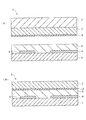
複数のシリコン基板を接着樹脂で貼り合わせて、3次元集積化した半導体装置を作製するため、シリコン基板の貼り合わせの予備実験を行なった。まず、図1に示すように、下側基板41と、薄化した上側基板42とを接着樹脂層43によって貼り合わせた後、上側基板42に貫通孔50を形成した。図1は、予備実験を行った場合の下側基板41及び上側基板42の断面図である。下側基板41及び上側基板42は、シリコン(Si)基板である。下側基板41の表面には、酸化シリコン膜44が形成されている。接着樹脂層43の材料として、BCB(benzo-cyclo-butene、ダウケミカル社製のサイクロテン(登録商標))樹脂を用いた。貫通孔50は、レジストマスクを用いてボッシュ法により上側基板42をエッチングすることにより形成した。上側基板42は、SF6とC48との混合ガ
スでエッチングし、接着樹脂層43は、CF4とO2との混合ガスでエッチングした。
In order to fabricate a three-dimensionally integrated semiconductor device by bonding a plurality of silicon substrates with an adhesive resin, a preliminary experiment for bonding silicon substrates was performed. First, as shown in FIG. 1, a lower substrate 41 and a thinned upper substrate 42 were bonded together by an adhesive resin layer 43, and then a through hole 50 was formed in the upper substrate 42. FIG. 1 is a cross-sectional view of the lower substrate 41 and the upper substrate 42 when a preliminary experiment is performed. The lower substrate 41 and the upper substrate 42 are silicon (Si) substrates. A silicon oxide film 44 is formed on the surface of the lower substrate 41. As a material of the adhesive resin layer 43, BCB (benzo-cyclo-butene, cycloten (registered trademark)) manufactured by Dow Chemical Co., Ltd. was used. The through hole 50 was formed by etching the upper substrate 42 by a Bosch method using a resist mask. The upper substrate 42 was etched with a mixed gas of SF 6 and C 4 F 8, and the adhesive resin layer 43 was etched with a mixed gas of CF 4 and O 2 .

図1に示すように、上側基板42に対しては、波状の凹形状であるスキャロップ形状51を有する貫通孔50が形成されている。接着樹脂層43は、上側基板42とはエッチング特性が異なる。そのため、エッチングが上側基板42から接着樹脂層43に進む際にサイドエッチングが生じて、上側基板42の底面に入り込むアンダーカット52が発生した
。したがって、図1に示すように、上側基板42における貫通孔50の側面にはスキャロップ形状51が形成され、接着樹脂層43における貫通孔50の側面にはアンダーカット52が形成された。アンダーカット52は、幅5μm程度であった。図2は、図1の部分拡大図であり、スキャロップ形状51及びアンダーカット52が形成された部分の断面観察写真のスケッチである。
As shown in FIG. 1, a through hole 50 having a scalloped shape 51 that is a wavy concave shape is formed in the upper substrate 42. The adhesive resin layer 43 is different in etching characteristics from the upper substrate 42. Therefore, side etching occurs when etching proceeds from the upper substrate 42 to the adhesive resin layer 43, and an undercut 52 that enters the bottom surface of the upper substrate 42 occurs. Therefore, as shown in FIG. 1, a scalloped shape 51 is formed on the side surface of the through hole 50 in the upper substrate 42, and an undercut 52 is formed on the side surface of the through hole 50 in the adhesive resin layer 43. The undercut 52 had a width of about 5 μm. FIG. 2 is a partially enlarged view of FIG. 1, and is a sketch of a cross-sectional observation photograph of a portion where a scallop shape 51 and an undercut 52 are formed.

上側基板42及び接着樹脂層43に貫通孔50を形成した後、貫通孔50の中にバリア絶縁膜(SiN膜)45を化学気相堆積(CVD、Chemical Vapor Deposition)法で堆
積した。そして、バリア絶縁膜45の上に、バリアメタル層(Ti層)46、Cuシード層をスパッタリングで形成した。更に、Cuシード層の上に、電解メッキによって銅(Cu)をメッキすることによって、貫通孔50の中にビア導電体47を埋め込んだ。図3は、貫通孔50の中に、バリア絶縁膜45、バリアメタル層46及びビア導電体47を形成した場合の下側基板41及び上側基板42の断面観察写真のスケッチである。
After the through holes 50 were formed in the upper substrate 42 and the adhesive resin layer 43, a barrier insulating film (SiN film) 45 was deposited in the through holes 50 by a chemical vapor deposition (CVD) method. Then, a barrier metal layer (Ti layer) 46 and a Cu seed layer were formed on the barrier insulating film 45 by sputtering. Furthermore, the via conductor 47 was embedded in the through hole 50 by plating copper (Cu) on the Cu seed layer by electrolytic plating. FIG. 3 is a sketch of cross-sectional observation photographs of the lower substrate 41 and the upper substrate 42 when the barrier insulating film 45, the barrier metal layer 46, and the via conductor 47 are formed in the through hole 50.

スキャロップ形状51及びアンダーカット52が生じると、貫通孔50の中にバリア絶縁膜45を化学気相堆積法で堆積した場合、バリア絶縁膜45が堆積される位置によっては、バリア絶縁膜45の被覆率(カバレッジ)が低下する。また、バリアメタル層46及びCuシード層の被覆率も低下する。バリア絶縁膜45、バリアメタル層46又はCuシード層が存在しない部分、或いは、薄い部分では、銅がメッキされない可能性がある。また、貫通孔50の中にボイド48が発生する可能性がある。更に、メッキされた銅が、バリア絶縁膜45及びバリアメタル層46を通過し、銅と上側基板42のシリコンとが反応することによりシリサイド49が形成される。シリサイド49が形成されると、貫通孔50の中に形成されたビア導電体47の抵抗を高くする可能性がある。また、銅が上側基板42の中に拡散すると、半導体装置のデバイス特性が劣化する可能性がある。   When the scalloped shape 51 and the undercut 52 occur, when the barrier insulating film 45 is deposited in the through hole 50 by the chemical vapor deposition method, the barrier insulating film 45 may be covered depending on the position where the barrier insulating film 45 is deposited. The rate (coverage) decreases. In addition, the coverage of the barrier metal layer 46 and the Cu seed layer also decreases. There is a possibility that copper is not plated in a portion where the barrier insulating film 45, the barrier metal layer 46 or the Cu seed layer is not present, or in a thin portion. Further, the void 48 may be generated in the through hole 50. Further, the plated copper passes through the barrier insulating film 45 and the barrier metal layer 46, and the silicide 49 is formed by the reaction between the copper and the silicon of the upper substrate 42. If the silicide 49 is formed, there is a possibility that the resistance of the via conductor 47 formed in the through hole 50 is increased. Further, when copper diffuses into the upper substrate 42, the device characteristics of the semiconductor device may be deteriorated.

図3に示すように、バリア絶縁膜45は所々薄く形成され、バリアメタル層46は全く形成されていない部分もあった。また、図3に示すように、ボイド48及びシリサイド49の形成も確認された。貫通孔50に形成されたスキャロップ形状51及びアンダーカット52を修復し、バリア絶縁膜45、バリアメタル層46及びCuシード層の被覆性を向上させることにより、良好なデバイス特性を有する半導体装置を製造することが可能になる。   As shown in FIG. 3, the barrier insulating film 45 is formed thin in some places, and there is a portion where the barrier metal layer 46 is not formed at all. In addition, as shown in FIG. 3, formation of voids 48 and silicide 49 was also confirmed. By repairing the scalloped shape 51 and the undercut 52 formed in the through hole 50 and improving the coverage of the barrier insulating film 45, the barrier metal layer 46, and the Cu seed layer, a semiconductor device having good device characteristics is manufactured. It becomes possible to do.

図4は、上側基板42及び接着樹脂層43に貫通孔50を形成した後に、上側基板42の上に閉塞材60を滴下し、スキージにより貫通孔50の中に閉塞材60を刷り込んだ場合の下側基板41及び上側基板42の断面図である。閉塞剤60として、AE1650(アサヒ化学研究所製、粘度2000dPa・s)とアロニックスM−350(東亜合成株式会社製)とを95wt%:5wt%の比率で混合したものを使用した。貫通孔50は閉空間となっており、貫通孔50の中に閉塞材60を刷り込む際に、貫通孔50の中の空気の逃げ場がなくなり、貫通孔50に対する閉塞剤60の正常な埋め込みが困難であった。   FIG. 4 shows a case where the through hole 50 is formed in the upper substrate 42 and the adhesive resin layer 43, and then the closing material 60 is dropped on the upper substrate 42 and the closing material 60 is imprinted in the through hole 50 by the squeegee. 4 is a cross-sectional view of a lower substrate 41 and an upper substrate 42. FIG. As the occlusive agent 60, AE1650 (manufactured by Asahi Chemical Research Laboratory, viscosity 2000 dPa · s) and Aronix M-350 (manufactured by Toagosei Co., Ltd.) mixed at a ratio of 95 wt%: 5 wt% were used. The through hole 50 is a closed space, and when the blocking material 60 is imprinted in the through hole 50, there is no escape space for air in the through hole 50, and normal filling of the blocking agent 60 in the through hole 50 is difficult. Met.

以下、図面を参照して、実施形態に係る半導体装置及び半導体装置の製造方法について、実施例を挙げて説明する。以下の実施例の構成は例示であり、本実施形態は実施例の構成に限定されない。   Hereinafter, a semiconductor device and a method for manufacturing the semiconductor device according to the embodiment will be described with reference to the drawings. The configurations of the following examples are illustrative, and the present embodiment is not limited to the configurations of the examples.

実施例1に係る半導体装置及びその製造方法について説明する。図5から図8及び図10から図15は、実施例1に係る下側基板1及び上側基板2を3次元的に積層した半導体装置3の要部断面図であり、実施例1に係る半導体装置3の製造方法を概略的に示している。   A semiconductor device and a manufacturing method thereof according to the first embodiment will be described. FIGS. 5 to 8 and FIGS. 10 to 15 are cross-sectional views of the main part of the semiconductor device 3 in which the lower substrate 1 and the upper substrate 2 according to the first embodiment are three-dimensionally stacked, and the semiconductor according to the first embodiment. The manufacturing method of the apparatus 3 is shown schematically.

まず、図5の(A)に示すように、表面に半導体集積回路(図示せず)が形成された下側基板1の表面上に配線層4を形成する。下側基板1は、例えば、シリコン(Si)基板である。例えば、下側基板1の表面上に、銅(Cu)層をスパッタリング又はメッキ等により形成し、レジストパターンをマスクとして銅層をエッチングすることにより、下側基板1の表面上に配線層4を形成する。なお、既に配線層4が下側基板1の表面上に形成されている場合、既に形成されている配線層4を利用してもよい。   First, as shown in FIG. 5A, a wiring layer 4 is formed on the surface of the lower substrate 1 on which a semiconductor integrated circuit (not shown) is formed. The lower substrate 1 is, for example, a silicon (Si) substrate. For example, a wiring layer 4 is formed on the surface of the lower substrate 1 by forming a copper (Cu) layer on the surface of the lower substrate 1 by sputtering or plating and etching the copper layer using the resist pattern as a mask. Form. If the wiring layer 4 has already been formed on the surface of the lower substrate 1, the wiring layer 4 that has already been formed may be used.

次に、図5の(B)に示すように、下側基板1の表面上に接着層5を形成する。例えば、下側基板1の表面上に、有機接着剤膜又は無機接着剤膜をスピンコート法により塗布する。続いて、ベーキングを行い、有機接着剤膜又は無機接着剤膜の溶剤を蒸発させ、有機接着剤膜又は無機接着剤膜を仮硬化させることにより、下側基板1の表面上に接着層5を形成する。接着層5の高さは、任意の値に設定することが可能であるが、配線層4の高さよりも低くならないようにする。例えば、接着層5の高さを約4μmとしてもよい。有機接着剤膜の材料として、BCB(benzo-cyclo-butene、ダウケミカル社製のサイクロテン(登録商標))樹脂を用いてもよい。有機接着剤膜の材料として、BCB樹脂を用いる場合、150℃でベーキングが行われる。   Next, as shown in FIG. 5B, the adhesive layer 5 is formed on the surface of the lower substrate 1. For example, an organic adhesive film or an inorganic adhesive film is applied on the surface of the lower substrate 1 by a spin coating method. Subsequently, baking is performed, the solvent of the organic adhesive film or the inorganic adhesive film is evaporated, and the organic adhesive film or the inorganic adhesive film is temporarily cured, whereby the adhesive layer 5 is formed on the surface of the lower substrate 1. Form. The height of the adhesive layer 5 can be set to an arbitrary value, but it should not be lower than the height of the wiring layer 4. For example, the height of the adhesive layer 5 may be about 4 μm. As a material for the organic adhesive film, BCB (benzo-cyclo-butene, cycloten (registered trademark)) manufactured by Dow Chemical Company may be used. When a BCB resin is used as the material for the organic adhesive film, baking is performed at 150 ° C.

そして、図6の(A)に示すように、表面に半導体集積回路(図示せず)が形成された上側基板2を、下側基板1の上方に位置決めする。上側基板2は、例えば、シリコン(Si)基板である。上側基板2の裏面を研削及び研磨することにより、上側基板2の厚さを調整している。上側基板2の調整後の厚さは、約40μmである。上側基板2の裏面には、酸化シリコン膜6が形成されている。例えば、化学気相堆積(CVD)法により、酸化シリコン膜6を形成してもよい。酸化シリコン膜6は、配線層4から上側基板2に銅等の金属が拡散することを抑止するための保護膜として機能する。ただし、上側基板2の裏面に、酸化シリコン膜6を形成しなくてもよい。   Then, as shown in FIG. 6A, the upper substrate 2 having a semiconductor integrated circuit (not shown) formed on the surface is positioned above the lower substrate 1. The upper substrate 2 is, for example, a silicon (Si) substrate. The thickness of the upper substrate 2 is adjusted by grinding and polishing the back surface of the upper substrate 2. The adjusted thickness of the upper substrate 2 is about 40 μm. A silicon oxide film 6 is formed on the back surface of the upper substrate 2. For example, the silicon oxide film 6 may be formed by chemical vapor deposition (CVD). The silicon oxide film 6 functions as a protective film for preventing metal such as copper from diffusing from the wiring layer 4 to the upper substrate 2. However, the silicon oxide film 6 may not be formed on the back surface of the upper substrate 2.

下側基板1及び上側基板2の位置合わせは、下側基板1及び上側基板2に予め形成したアライメントマークを用いて行う。上側基板2の表面側にガラス基板等の支持基板7が仮接着されており、支持基板7により上側基板2を支持した状態で、下側基板1及び上側基板2の位置合わせが行われている。また、下側基板1の表面と上側基板2の裏面とが向かい合うように、下側基板1及び上側基板2の位置合わせが行われている。上側基板2と支持基板7との仮接着には、熱発泡性の接着剤を用いてもよい。上側基板2と支持基板7との仮接着に用いる接着剤は、後に簡便に剥離することが可能であれば特に限定されず、一般的な熱発泡性接着剤や紫外線発泡性接着剤を用いてもよい。   The alignment of the lower substrate 1 and the upper substrate 2 is performed using alignment marks formed in advance on the lower substrate 1 and the upper substrate 2. A support substrate 7 such as a glass substrate is temporarily bonded to the surface side of the upper substrate 2, and the lower substrate 1 and the upper substrate 2 are aligned with the upper substrate 2 supported by the support substrate 7. . The lower substrate 1 and the upper substrate 2 are aligned so that the front surface of the lower substrate 1 and the back surface of the upper substrate 2 face each other. For temporary adhesion between the upper substrate 2 and the support substrate 7, a heat foaming adhesive may be used. The adhesive used for temporary adhesion between the upper substrate 2 and the support substrate 7 is not particularly limited as long as it can be easily peeled later, and a general thermal foaming adhesive or ultraviolet foaming adhesive is used. Also good.

次いで、図6の(B)に示すように、下側基板1及び上側基板2の位置合わせを行った後、下側基板1と上側基板2とを接触させ、加熱加圧下において、下側基板1と上側基板2とを接着させる。すなわち、下側基板1と上側基板2との間に接着層5を配置し、接着層5を介して下側基板1の表面と上側基板2の裏面とを接着させる。例えば、積層配置した下側基板1及び上側基板2を、真空雰囲気下において、250℃で60分、下側基板1及び上側基板2の両方又は一方を加圧することにより、下側基板1と上側基板2との接着を行う。その後、支持基板7を上側基板2から剥離する。上述したように、接着層5の高さは、任意の値に設定することが可能であり、接着層5の高さを所望の値に設定することにより、下側基板1と上側基板2との基板間距離を所望の値に設定することが可能である。例えば、接着層5の高さを、上側基板2の厚さの10分の1とすることにより、下側基板1と上側基板2との基板間距離を上側基板2の厚さの10分の1とすることが可能である。   Next, as shown in FIG. 6B, after the lower substrate 1 and the upper substrate 2 are aligned, the lower substrate 1 and the upper substrate 2 are brought into contact with each other, and the lower substrate is heated and pressurized. 1 and the upper substrate 2 are bonded. That is, the adhesive layer 5 is disposed between the lower substrate 1 and the upper substrate 2, and the surface of the lower substrate 1 and the back surface of the upper substrate 2 are bonded via the adhesive layer 5. For example, the lower substrate 1 and the upper substrate 2 arranged in a stacked manner are pressurized by pressing either or both of the lower substrate 1 and the upper substrate 2 in a vacuum atmosphere at 250 ° C. for 60 minutes. Bonding with the substrate 2 is performed. Thereafter, the support substrate 7 is peeled from the upper substrate 2. As described above, the height of the adhesive layer 5 can be set to an arbitrary value. By setting the height of the adhesive layer 5 to a desired value, the lower substrate 1 and the upper substrate 2 The distance between the substrates can be set to a desired value. For example, by setting the height of the adhesive layer 5 to 1/10 of the thickness of the upper substrate 2, the distance between the lower substrate 1 and the upper substrate 2 can be reduced to 10 minutes of the thickness of the upper substrate 2. 1 is possible.

次に、図7に示すように、上側基板2の表面上に、貫通孔位置の上方に開口を有するフォトレジストパターン8を形成する。例えば、上側基板2の表面上にフォトレジスト膜を
塗布した後、露光装置を用いてフォトレジスト膜を露光することにより、フォトレジストパターン8を形成する。上側基板2は、アライメントマークを用いて下側基板1に位置合わせして接着してあるので、上側基板2のアライメントマークを基準にして、貫通孔位置の上方に開口を有するフォトレジストパターン8を形成することが可能である。
Next, as shown in FIG. 7, a photoresist pattern 8 having an opening above the position of the through hole is formed on the surface of the upper substrate 2. For example, after a photoresist film is applied on the surface of the upper substrate 2, the photoresist film is exposed using an exposure apparatus, thereby forming a photoresist pattern 8. Since the upper substrate 2 is aligned and adhered to the lower substrate 1 using the alignment mark, the photoresist pattern 8 having an opening above the through hole position is formed with reference to the alignment mark of the upper substrate 2. It is possible to form.

そして、図7に示すように、フォトレジストパターン8をマスクとして、ボッシュ法を用いて上側基板2、酸化シリコン膜6及び接着層5をエッチングすることにより、上側基板2、酸化シリコン膜6及び接着層5を貫通する貫通孔9を、上側基板2、酸化シリコン膜6及び接着層5に形成する。すなわち、上側基板2の表面から配線層4まで達する貫通孔9を、上側基板2、酸化シリコン膜6及び接着層5に形成する。上側基板2及び酸化シリコン膜6は、SF6とC48との混合ガスでエッチングを行い、接着層5は、CF4とO2との混合ガスでエッチングを行う。その後、アッシング(灰化処理)により、フォトレ
ジストパターン8を除去する。
Then, as shown in FIG. 7, the upper substrate 2, the silicon oxide film 6, and the adhesive layer 5 are etched using the Bosch method using the photoresist pattern 8 as a mask, thereby bonding the upper substrate 2, the silicon oxide film 6, and the adhesive A through hole 9 penetrating the layer 5 is formed in the upper substrate 2, the silicon oxide film 6 and the adhesive layer 5. That is, a through hole 9 reaching from the surface of the upper substrate 2 to the wiring layer 4 is formed in the upper substrate 2, the silicon oxide film 6, and the adhesive layer 5. The upper substrate 2 and the silicon oxide film 6 are etched with a mixed gas of SF 6 and C 4 F 8, and the adhesive layer 5 is etched with a mixed gas of CF 4 and O 2 . Thereafter, the photoresist pattern 8 is removed by ashing (ashing treatment).

ボッシュ法を用いて上側基板2、酸化シリコン膜6及び接着層5をエッチングしているので、図7に示すように、上側基板2及び酸化シリコン膜6に対しては、波状の凹形状であるスキャロップ形状10を有する貫通孔9が形成される。接着層5は、上側基板2及び酸化シリコン膜6とはエッチング特性が異なる。そのため、エッチングが上側基板2及び酸化シリコン膜6から接着層5に進む際にサイドエッチングが生じて、上側基板2の下方に入り込むアンダーカット11が発生する。したがって、図7に示すように、上側基板2及び酸化シリコン膜6における貫通孔9の側面にはスキャロップ形状10が形成され、接着層5における貫通孔9の側面にはアンダーカット11が形成される。すなわち、上側基板2、酸化シリコン膜6及び接着層5の貫通孔9の側面には、凹部が形成されている。スキャロップ形状10及びアンダーカット11は、凹部の一例である。   Since the upper substrate 2, the silicon oxide film 6 and the adhesive layer 5 are etched using the Bosch method, the upper substrate 2 and the silicon oxide film 6 have a wavy concave shape as shown in FIG. A through hole 9 having a scallop shape 10 is formed. The adhesive layer 5 is different in etching characteristics from the upper substrate 2 and the silicon oxide film 6. Therefore, side etching occurs when etching proceeds from the upper substrate 2 and the silicon oxide film 6 to the adhesive layer 5, and an undercut 11 that enters below the upper substrate 2 occurs. Therefore, as shown in FIG. 7, a scallop shape 10 is formed on the side surface of the through hole 9 in the upper substrate 2 and the silicon oxide film 6, and an undercut 11 is formed on the side surface of the through hole 9 in the adhesive layer 5. . That is, concave portions are formed on the side surfaces of the upper substrate 2, the silicon oxide film 6 and the through holes 9 of the adhesive layer 5. The scallop shape 10 and the undercut 11 are an example of a recessed part.

そして、図8に示すように、貫通孔9の中に閉塞樹脂12が埋め込まれるように、上側基板2の表面上に閉塞樹脂12をスピンコート法により塗布する。すなわち、貫通孔9を閉塞樹脂12で埋める。続いて、ベーキングを行い、閉塞樹脂12の溶剤を蒸発させ、閉塞樹脂12を仮硬化させる。その後、低酸素オーブンにおいて1時間のベーキングを行い、閉塞樹脂12を本硬化させる。閉塞樹脂12を完全又は略完全に硬化させる前の半硬化状態を、本明細書では、仮硬化と表記する。また、閉塞樹脂12を完全又は略完全に硬化させることを、本明細書では、本硬化と表記する。閉塞樹脂12として、有機骨格を有する無機有機のハイブリッド樹脂を用いてもよい。無機有機のハイブリッド樹脂は、例えば、PTS−R(ハネウェル社製、粘度9mPa・s)がある。閉塞樹脂12としてPTS−Rを用いる場合、110℃でベーキングを行うことにより閉塞樹脂12を仮硬化させ、200℃でベーキングを行うことにより閉塞樹脂12を本硬化させる。   Then, as shown in FIG. 8, the closing resin 12 is applied on the surface of the upper substrate 2 by a spin coating method so that the closing resin 12 is embedded in the through hole 9. That is, the through hole 9 is filled with the closing resin 12. Subsequently, baking is performed to evaporate the solvent of the plugging resin 12, and the plugging resin 12 is temporarily cured. Thereafter, baking is performed for 1 hour in a low-oxygen oven to fully cure the blocking resin 12. In this specification, the semi-cured state before completely or substantially completely curing the blocking resin 12 is referred to as temporary curing. Further, in the present specification, curing the blocking resin 12 completely or substantially completely is referred to as main curing. As the blocking resin 12, an inorganic-organic hybrid resin having an organic skeleton may be used. An example of the inorganic-organic hybrid resin is PTS-R (manufactured by Honeywell, viscosity 9 mPa · s). When PTS-R is used as the blocking resin 12, the blocking resin 12 is temporarily cured by baking at 110 ° C., and the blocking resin 12 is fully cured by baking at 200 ° C.

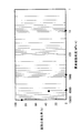
ここで、閉塞樹脂12の粘度と、貫通孔9に閉塞樹脂12を埋め込んだ場合の貫通孔9における空隙の発生率との関係について説明する。閉塞樹脂12の粘度と、貫通孔9に閉塞樹脂12を埋め込んだ場合の貫通孔9における空隙の発生率との関係を調査した。閉塞樹脂12は、PTS−Rを使用し、濃縮法によりPTS−R中の溶剤成分を揮発させて、閉塞樹脂12の粘度を調節した。図9は、閉塞樹脂12の粘度(mPa・s)と、貫通孔9に閉塞樹脂12を埋め込んだ場合の貫通孔9における空隙の発生率(%)との関係を示すグラフである。図9の縦軸は、貫通孔9に閉塞樹脂12を埋め込んだ場合の貫通孔9における空隙の発生率(%)を示しており、図9の横軸は、閉塞樹脂12の粘度(mPa・s)を示している。図9の◆は、各粘度における閉塞樹脂12を、貫通孔9に埋め込んだ後に貫通孔9の断面を観察することによって得た貫通孔9における空隙の発生率をプロットしたものである。   Here, the relationship between the viscosity of the blocking resin 12 and the occurrence rate of voids in the through hole 9 when the blocking resin 12 is embedded in the through hole 9 will be described. The relationship between the viscosity of the blocking resin 12 and the occurrence rate of voids in the through hole 9 when the blocking resin 12 was embedded in the through hole 9 was investigated. As the occlusion resin 12, PTS-R was used, and the viscosity of the occlusion resin 12 was adjusted by volatilizing the solvent component in the PTS-R by a concentration method. FIG. 9 is a graph showing the relationship between the viscosity (mPa · s) of the closing resin 12 and the occurrence rate (%) of voids in the through hole 9 when the closing resin 12 is embedded in the through hole 9. The vertical axis in FIG. 9 shows the generation rate (%) of voids in the through holes 9 when the through resin 9 is embedded in the through holes 9, and the horizontal axis in FIG. 9 shows the viscosity (mPa · s). In FIG. 9, ♦ is a plot of the incidence of voids in the through-holes 9 obtained by observing the cross-section of the through-holes 9 after the plugging resin 12 at each viscosity is embedded in the through-holes 9.

閉塞樹脂12の粘度が4000mPa・s以下になると、貫通孔9における空隙の発生
率(%)が0%又は0%付近になることが、図9に示すグラフから読み取れる。したがって、閉塞樹脂12の粘度を4000mPa・s以下に調整することにより、貫通孔9に対する閉塞樹脂12の埋め込み性を大幅に向上することができる。図9に示す結果から、閉塞樹脂12の粘度は、4000mPa・s以下であることが好ましい。閉塞樹脂12の粘度を所定値以下(例えば、4000mPa・s以下)に調整することにより、貫通孔9の中における空気相の発生を抑制しつつ、貫通孔9の中に閉塞樹脂12を埋め込むことが可能となる。すなわち、閉塞樹脂12の粘度を所定値以下(例えば、4000mPa・s以下)にすることにより、スキャロップ形状10及びアンダーカット11における閉塞樹脂12の埋め込み率を上昇させることが可能となる。
It can be seen from the graph shown in FIG. 9 that when the viscosity of the blocking resin 12 is 4000 mPa · s or less, the void generation rate (%) in the through-hole 9 is 0% or near 0%. Therefore, by adjusting the viscosity of the closing resin 12 to 4000 mPa · s or less, the embedding property of the closing resin 12 in the through hole 9 can be greatly improved. From the results shown in FIG. 9, it is preferable that the viscosity of the blocking resin 12 is 4000 mPa · s or less. By adjusting the viscosity of the blocking resin 12 to a predetermined value or less (for example, 4000 mPa · s or less), the blocking resin 12 is embedded in the through hole 9 while suppressing the generation of an air phase in the through hole 9. Is possible. That is, by setting the viscosity of the blocking resin 12 to a predetermined value or less (for example, 4000 mPa · s or less), it is possible to increase the filling rate of the blocking resin 12 in the scallop shape 10 and the undercut 11.

また、閉塞樹脂12は、少なくとも有機骨格を有する樹脂であることが好ましい。閉塞樹脂12が少なくとも有機骨格を有することにより、閉塞樹脂12を硬化させる場合において、スキャロップ形状10及びアンダーカット11に埋め込まれた閉塞樹脂12の内部応力によるクラックの発生を抑制することが可能となる。また、閉塞樹脂12が少なくとも有機骨格を有することにより、閉塞樹脂12を硬化させる場合において、上側基板2又は接着層5と閉塞樹脂12との界面剥離の発生を抑制することが可能となる。   Further, the closing resin 12 is preferably a resin having at least an organic skeleton. When the plugging resin 12 has at least an organic skeleton, it is possible to suppress the occurrence of cracks due to internal stress of the plugging resin 12 embedded in the scallop shape 10 and the undercut 11 when the plugging resin 12 is cured. . In addition, since the blocking resin 12 has at least an organic skeleton, it is possible to suppress the occurrence of interface peeling between the upper substrate 2 or the adhesive layer 5 and the blocking resin 12 when the blocking resin 12 is cured.

次いで、図10に示すように、リアクティブイオンエッチング(RIE)法を用いて異方性エッチングすることにより、閉塞樹脂12を貫通する貫通孔13を、閉塞樹脂12に形成する。図10に示すように、貫通孔13は、配線層4まで達している。閉塞樹脂12は、上側基板2、酸化シリコン膜6及び接着層5を貫通する貫通孔9の中に埋め込み形成されており、貫通孔13は、閉塞樹脂12を貫通している。したがって、貫通孔13は、上側基板2、酸化シリコン膜6及び接着層5を貫通している。   Next, as shown in FIG. 10, through holes 13 penetrating the blocking resin 12 are formed in the blocking resin 12 by anisotropic etching using a reactive ion etching (RIE) method. As shown in FIG. 10, the through hole 13 reaches the wiring layer 4. The closing resin 12 is embedded in a through hole 9 that penetrates the upper substrate 2, the silicon oxide film 6, and the adhesive layer 5, and the through hole 13 passes through the closing resin 12. Accordingly, the through hole 13 penetrates the upper substrate 2, the silicon oxide film 6 and the adhesive layer 5.

貫通孔13を形成する際に用いられるエッチングガスは、CF4とO2との混合ガスである。そのためCF4とO2との混合ガスを用いたエッチングは、閉塞樹脂12に対するエッチング量が大きく、上側基板2に対するエッチング量が小さい。したがって、上側基板2の表面上に形成された閉塞樹脂12及び貫通孔9の中に埋め込み形成された閉塞樹脂12がエッチングにより除去されるが、上側基板2は除去されずに残存する。また、貫通孔13を形成する際のエッチングは、異方性エッチングである。そのため、上側基板2の表面方向から見て上側基板2の蔭になる部分の閉塞樹脂12、すなわち、上側基板2の下方に存在する閉塞樹脂12は、異方性エッチングによっては除去されない。したがって、上側基板2のスキャロップ形状10の窪んだ部分及び接着層5のアンダーカット11の窪んだ部分に埋め込まれている閉塞樹脂12は除去されずに残存する。すなわち、上側基板2のスキャロップ形状10の窪んだ部分及び接着層5のアンダーカット11の窪んだ部分には、閉塞樹脂12が埋められた状態となっている。このように、閉塞樹脂12に対するエッチング量が大きく、上側基板2に対するエッチング量が小さいエッチングガスを用いて異方性エッチングを行うことにより、マスクを要せずに、貫通孔13を形成することが可能である。 The etching gas used when forming the through-hole 13 is a mixed gas of CF 4 and O 2 . Therefore, the etching using the mixed gas of CF 4 and O 2 has a large etching amount with respect to the blocking resin 12 and a small etching amount with respect to the upper substrate 2. Therefore, the closing resin 12 formed on the surface of the upper substrate 2 and the closing resin 12 embedded in the through hole 9 are removed by etching, but the upper substrate 2 remains without being removed. The etching for forming the through holes 13 is anisotropic etching. Therefore, the portion of the blocking resin 12 that becomes a ridge of the upper substrate 2 when viewed from the surface direction of the upper substrate 2, that is, the blocking resin 12 existing below the upper substrate 2 is not removed by anisotropic etching. Therefore, the blocking resin 12 embedded in the recessed portion of the scalloped shape 10 of the upper substrate 2 and the recessed portion of the undercut 11 of the adhesive layer 5 remains without being removed. That is, the blocking resin 12 is buried in the recessed portion of the scalloped shape 10 of the upper substrate 2 and the recessed portion of the undercut 11 of the adhesive layer 5. Thus, by performing anisotropic etching using an etching gas having a large etching amount with respect to the blocking resin 12 and a small etching amount with respect to the upper substrate 2, the through hole 13 can be formed without using a mask. Is possible.

例えば、上側基板2のスキャロップ形状10の窪んだ部分を貫通孔9の外周とし、上側基板2のスキャロップ形状10の突出した部分を貫通孔13の外周とする場合、貫通孔13の径は、貫通孔9の径よりも小さい。実施例1における一例では、例えば、貫通孔9の径を22μmとした場合、貫通孔13の径は20μmとなった。したがって、貫通孔9の径は、貫通孔13の径よりも大きい。ただし、貫通孔9及び13の径の数値は、任意の値に設定することが可能であり、貫通孔9及び13の径の数値は、実施例1における数値に限定されるものではない。   For example, when the recessed portion of the scallop shape 10 of the upper substrate 2 is the outer periphery of the through hole 9 and the protruding portion of the scallop shape 10 of the upper substrate 2 is the outer periphery of the through hole 13, the diameter of the through hole 13 is It is smaller than the diameter of the hole 9. In an example in Example 1, for example, when the diameter of the through hole 9 is 22 μm, the diameter of the through hole 13 is 20 μm. Therefore, the diameter of the through hole 9 is larger than the diameter of the through hole 13. However, the numerical values of the diameters of the through holes 9 and 13 can be set to arbitrary values, and the numerical values of the diameters of the through holes 9 and 13 are not limited to the numerical values in the first embodiment.

次に、図11に示すように、プラズマCVD(plasma-enhanced CVD)法により絶縁性バリア膜20を、上側基板2の表面(上面)、貫通孔13の側面及び底面に形成する。
絶縁性バリア膜20は、例えば、窒化シリコン(SiN)膜である。実施例1における一例では、例えば、シラン(SiH4)及びアンモニア(NH3)をソースガスとし、300℃のプラズマCVD法により厚さ200nm程度の窒化シリコン膜を、上側基板2の表面上及び貫通孔13の側面に形成した。実施例1における一例では、貫通孔13の底面には、厚さ120nm程度の窒化シリコン膜が形成された。このように、実施例1に係る半導体装置3の製造方法においては、貫通孔13の側面に絶縁性バリア膜20を良好に被覆することが可能である。すなわち、実施例1に係る半導体装置3の製造方法においては、絶縁性バリア膜20の被覆性を低下させずに、貫通孔13の側面に絶縁性バリア膜20を被覆することが可能である。
Next, as shown in FIG. 11, an insulating barrier film 20 is formed on the surface (upper surface) of the upper substrate 2, the side surfaces and the bottom surface of the through-hole 13 by plasma CVD (plasma-enhanced CVD).
The insulating barrier film 20 is, for example, a silicon nitride (SiN) film. In an example in the first embodiment, for example, silane (SiH 4 ) and ammonia (NH 3 ) are used as a source gas, and a silicon nitride film having a thickness of about 200 nm is formed on and through the surface of the upper substrate 2 by a plasma CVD method at 300 ° C. It was formed on the side surface of the hole 13. In one example in Example 1, a silicon nitride film having a thickness of about 120 nm was formed on the bottom surface of the through hole 13. Thus, in the method for manufacturing the semiconductor device 3 according to the first embodiment, it is possible to satisfactorily coat the insulating barrier film 20 on the side surface of the through hole 13. That is, in the method for manufacturing the semiconductor device 3 according to the first embodiment, the insulating barrier film 20 can be coated on the side surface of the through-hole 13 without reducing the covering property of the insulating barrier film 20.

そして、図12に示すように、リアクティブイオンエッチング(RIE)法により、CF4とO2との混合ガスを用いた異方性エッチングを行うことにより、上側基板2の表面に形成された絶縁性バリア膜20、貫通孔13の底面に形成された絶縁性バリア膜20を除去する。 Then, as shown in FIG. 12, the insulation formed on the surface of the upper substrate 2 by performing anisotropic etching using a mixed gas of CF 4 and O 2 by reactive ion etching (RIE). The insulating barrier film 20 and the insulating barrier film 20 formed on the bottom surface of the through hole 13 are removed.

次いで、図13に示すように、スパッタリング等の物理的気相堆積(PVD、physical
vapor deposition)法により、バリアメタル層21を、上側基板2の表面、貫通孔13
の側面及び底面に形成する。バリアメタル層21は、例えば、Tiライナ等である。バリアメタル層21の厚さは、例えば、100nm程度である。次に、図13に示すように、スパッタリング等の物理的気相堆積(PVD)法により、シード層22をバリアメタル層21の表面上に形成する。シード層22は、例えば、銅である。シード層22の厚さは、例えば、250nm程度である。
Next, as shown in FIG. 13, physical vapor deposition (PVD, physical, such as sputtering).
The barrier metal layer 21 is formed on the surface of the upper substrate 2 and the through hole 13 by vapor deposition).
Formed on the side and bottom surfaces. The barrier metal layer 21 is, for example, a Ti liner. The thickness of the barrier metal layer 21 is, for example, about 100 nm. Next, as shown in FIG. 13, a seed layer 22 is formed on the surface of the barrier metal layer 21 by a physical vapor deposition (PVD) method such as sputtering. The seed layer 22 is, for example, copper. The thickness of the seed layer 22 is, for example, about 250 nm.

実施例1に係る半導体装置3の製造方法においては、貫通孔13の側面に絶縁性バリア膜20が良好に被覆されている。したがって、実施例1に係る半導体装置3の製造方法においては、貫通孔13の側面にバリアメタル層21を良好に被覆することが可能である。この結果、実施例1に係る半導体装置3の製造方法においては、貫通孔13の側面にシード層22を良好に被覆することが可能である。実施例1に係る半導体装置3の製造方法においては、絶縁性バリア膜20、バリアメタル層21及びシード層22の被覆性を低下させずに、貫通孔13の側面に絶縁性バリア膜20、バリアメタル層21及びシード層22を被覆することが可能である。このように、実施例1に係る半導体装置3の製造方法によれば、貫通孔9に形成されたスキャロップ形状10及びアンダーカット11を修復することにより、絶縁性バリア膜20、バリアメタル膜21及びシード層22の被覆性を向上させることができる。   In the method for manufacturing the semiconductor device 3 according to the first embodiment, the insulating barrier film 20 is satisfactorily covered on the side surface of the through hole 13. Therefore, in the method for manufacturing the semiconductor device 3 according to the first embodiment, the side wall of the through hole 13 can be satisfactorily covered with the barrier metal layer 21. As a result, in the method for manufacturing the semiconductor device 3 according to the first embodiment, it is possible to satisfactorily cover the seed layer 22 on the side surface of the through hole 13. In the method for manufacturing the semiconductor device 3 according to the first embodiment, the insulating barrier film 20, the barrier is formed on the side surface of the through hole 13 without reducing the coverage of the insulating barrier film 20, the barrier metal layer 21, and the seed layer 22. It is possible to cover the metal layer 21 and the seed layer 22. Thus, according to the method for manufacturing the semiconductor device 3 according to the first embodiment, the insulating barrier film 20, the barrier metal film 21, and the undercut 11 are repaired by repairing the scallop shape 10 and the undercut 11 formed in the through hole 9. The coverage of the seed layer 22 can be improved.

次に、図14に示すように、バリアメタル層21及びシード層22を電極として、電解メッキ法により、シード層22の表面上にメッキ層を形成することにより、シード層22及びメッキ層を有する導電層23を、上側基板2の上方及び貫通孔13の中に形成する。メッキ層及び導電層23は、例えば、銅である。図14に示すように、貫通孔13の中にはボイドが生じていない。したがって、貫通孔13の中には、導電層23が完全又は略完全に埋め込まれている。   Next, as shown in FIG. 14, by using the barrier metal layer 21 and the seed layer 22 as an electrode, a plating layer is formed on the surface of the seed layer 22 by electrolytic plating, so that the seed layer 22 and the plating layer are provided. The conductive layer 23 is formed above the upper substrate 2 and in the through hole 13. The plating layer and the conductive layer 23 are, for example, copper. As shown in FIG. 14, no void is generated in the through hole 13. Therefore, the conductive layer 23 is completely or substantially completely embedded in the through hole 13.

そして、図15に示すように、化学機械研磨(chemical mechanical polishing、CM
P)等により、上側基板2及び貫通孔13の上方の導電層23を除去することにより、貫通孔13の中にビア導電体24を形成する。図15に示すように、配線層4の上方にビア導電体24が配置されている。すなわち、ビア導電体24の下方に配線層4が形成されている。
Then, as shown in FIG. 15, chemical mechanical polishing (CM)
The via conductor 24 is formed in the through hole 13 by removing the conductive layer 23 above the upper substrate 2 and the through hole 13 by P) or the like. As shown in FIG. 15, a via conductor 24 is disposed above the wiring layer 4. That is, the wiring layer 4 is formed below the via conductor 24.

必要に応じて、上側基板2の表面上や、ビア導電体24の表面上に、配線を形成してもよい。例えば、上側基板2の表面上及びビア導電体24の表面上に、銅層をスパッタリン
グ又はメッキ等により形成し、レジストパターンをマスクとして銅層をエッチングすることにより、上側基板2の表面上及びビア導電体24の表面上に配線を形成してもよい。更に、半導体基板を、上側基板2の上方に積層してもよい。
If necessary, wiring may be formed on the surface of the upper substrate 2 or on the surface of the via conductor 24. For example, a copper layer is formed on the surface of the upper substrate 2 and on the surface of the via conductor 24 by sputtering or plating, and the copper layer is etched using the resist pattern as a mask, so that the surface of the upper substrate 2 and the via are etched. A wiring may be formed on the surface of the conductor 24. Further, a semiconductor substrate may be stacked above the upper substrate 2.

実施例1に係る半導体装置3においては、ビア導電体24にはシリサイドは形成されておらず、上側基板2への銅の拡散も発生していない。したがって、実施例1に係る半導体装置3の製造方法によれば、良好なデバイス特性を有する半導体装置3を製造することが可能である。   In the semiconductor device 3 according to the first embodiment, no silicide is formed in the via conductor 24 and no copper is diffused into the upper substrate 2. Therefore, according to the method for manufacturing the semiconductor device 3 according to the first embodiment, it is possible to manufacture the semiconductor device 3 having good device characteristics.

ビア導電体24は、銅であるが、銅に代えて、アルミニウム(Al)又はタングステン(W)を、ビア導電体24として用いてもよい。この場合、シード層22及びメッキ層については、アルミニウム又はタングステンを用いればよい。   The via conductor 24 is copper, but aluminum (Al) or tungsten (W) may be used as the via conductor 24 instead of copper. In this case, aluminum or tungsten may be used for the seed layer 22 and the plating layer.

実施例2に係る半導体装置3及びその製造方法について説明する。なお、実施例1と同一の構成要素については、実施例1と同一の符号を付し、その説明を省略する。図16から図19は、実施例2に係る下側基板1及び上側基板2を3次元的に積層した半導体装置3の要部断面図であり、実施例2に係る半導体装置3の製造方法を概略的に示している。実施例2に係る半導体装置3の製造方法は、実施例1の図5から図8及び図10を用いて説明した工程と同様の工程を行った後、図16に示すように、スパッタリング等の物理的気相堆積法により、バリアメタル層30及び31を、上側基板2の表面、貫通孔13の側面及び底面に形成する。バリアメタル層30は、例えば、TiN層であり、バリアメタル層31は、例えば、Ti層である。バリアメタル層30の厚さは、例えば、100nm程度であり、バリアメタル層31の厚さは、例えば、100nm程度である。   A semiconductor device 3 and a manufacturing method thereof according to the second embodiment will be described. In addition, about the component same as Example 1, the code | symbol same as Example 1 is attached | subjected and the description is abbreviate | omitted. 16 to 19 are cross-sectional views of a main part of the semiconductor device 3 in which the lower substrate 1 and the upper substrate 2 according to the second embodiment are three-dimensionally stacked. The method for manufacturing the semiconductor device 3 according to the second embodiment is illustrated in FIGS. Shown schematically. The manufacturing method of the semiconductor device 3 according to the second embodiment is similar to that described with reference to FIGS. 5 to 8 and FIG. 10 of the first embodiment. Then, as shown in FIG. Barrier metal layers 30 and 31 are formed on the surface of the upper substrate 2 and the side and bottom surfaces of the through holes 13 by physical vapor deposition. The barrier metal layer 30 is, for example, a TiN layer, and the barrier metal layer 31 is, for example, a Ti layer. The thickness of the barrier metal layer 30 is, for example, about 100 nm, and the thickness of the barrier metal layer 31 is, for example, about 100 nm.

次に、図17に示すように、スパッタリング等の物理的気相堆積(PVD)法により、バリアメタル層31の表面上にシード層32を形成する。シード層32は、例えば、銅である。シード層32の厚さは、例えば、250nm程度である。   Next, as shown in FIG. 17, a seed layer 32 is formed on the surface of the barrier metal layer 31 by a physical vapor deposition (PVD) method such as sputtering. The seed layer 32 is, for example, copper. The thickness of the seed layer 32 is, for example, about 250 nm.

実施例2に係る半導体装置3の製造方法においては、貫通孔13の側面にバリアメタル層30及び31が良好に被覆されている。したがって、実施例2に係る半導体装置3の製造方法においては、貫通孔13の側面にシード層32を良好に被覆することが可能である。実施例2に係る半導体装置3の製造方法においては、バリアメタル層30、31及びシード層32の被覆性を低下させずに、貫通孔13の側面にバリアメタル層30、31及びシード層32を被覆することが可能である。このように、実施例1に係る半導体装置3の製造方法によれば、貫通孔9に形成されたスキャロップ形状10及びアンダーカット11を修復することにより、バリアメタル層30、31及びシード層32の被覆性を向上させることができる。   In the method for manufacturing the semiconductor device 3 according to the second embodiment, the side wall of the through-hole 13 is satisfactorily covered with the barrier metal layers 30 and 31. Therefore, in the method for manufacturing the semiconductor device 3 according to the second embodiment, it is possible to satisfactorily cover the seed layer 32 on the side surface of the through hole 13. In the method for manufacturing the semiconductor device 3 according to the second embodiment, the barrier metal layers 30, 31 and the seed layer 32 are formed on the side surface of the through hole 13 without reducing the coverage of the barrier metal layers 30, 31 and the seed layer 32. It is possible to coat. As described above, according to the method of manufacturing the semiconductor device 3 according to the first embodiment, the scallop shape 10 and the undercut 11 formed in the through hole 9 are repaired, whereby the barrier metal layers 30 and 31 and the seed layer 32 are formed. Coverability can be improved.

そして、図18に示すように、バリアメタル層30、31及びシード層32を電極として、電解メッキ法により、シード層32の表面上にメッキ層を形成することにより、シード層32及びメッキ層を有する導電層33を、上側基板2の上方及び貫通孔13の中に形成する。メッキ層及び導電層33は、例えば、銅である。図18に示すように、貫通孔13の中にはボイドが生じていない。したがって、貫通孔13の中には、導電層33が完全又は略完全に埋め込まれている。   Then, as shown in FIG. 18, the seed layer 32 and the plating layer are formed by forming a plating layer on the surface of the seed layer 32 by electrolytic plating using the barrier metal layers 30 and 31 and the seed layer 32 as electrodes. A conductive layer 33 is formed above the upper substrate 2 and in the through hole 13. The plating layer and the conductive layer 33 are, for example, copper. As shown in FIG. 18, no void is generated in the through hole 13. Therefore, the conductive layer 33 is completely or substantially completely embedded in the through hole 13.

次いで、図19に示すように、化学機械研磨(CMP)等により、上側基板2及び貫通孔13の上方の導電層33を除去することにより、貫通孔13の中にビア導電体34を形成する。図19に示すように、配線層4の上方にビア導電体34が配置されている。すなわち、ビア導電体34の下方に配線層4が形成されている。   Next, as shown in FIG. 19, the via conductor 34 is formed in the through hole 13 by removing the conductive layer 33 above the upper substrate 2 and the through hole 13 by chemical mechanical polishing (CMP) or the like. . As shown in FIG. 19, a via conductor 34 is disposed above the wiring layer 4. That is, the wiring layer 4 is formed below the via conductor 34.

必要に応じて、上側基板2の表面上や、ビア導電体34の表面上に、配線を形成してもよい。例えば、上側基板2の表面上及びビア導電体34の表面上に、銅層をスパッタリング又はメッキ等により形成し、レジストパターンをマスクとして銅層をエッチングすることにより、上側基板2の表面上及びビア導電体34の表面上に配線を形成してもよい。更に、半導体基板を、上側基板2の上方に積層してもよい。   If necessary, wiring may be formed on the surface of the upper substrate 2 or on the surface of the via conductor 34. For example, a copper layer is formed on the surface of the upper substrate 2 and the surface of the via conductor 34 by sputtering or plating, and the copper layer is etched using the resist pattern as a mask, so that the surface of the upper substrate 2 and the via are etched. A wiring may be formed on the surface of the conductor 34. Further, a semiconductor substrate may be stacked above the upper substrate 2.

実施例2に係る半導体装置3においては、ビア導電体34にはシリサイドは形成されておらず、上側基板2への銅の拡散も発生していない。したがって、実施例2に係る半導体装置3の製造方法によれば、良好なデバイス特性を有する半導体装置3を製造することが可能である。   In the semiconductor device 3 according to the second embodiment, no silicide is formed on the via conductor 34 and no copper is diffused into the upper substrate 2. Therefore, according to the method for manufacturing the semiconductor device 3 according to the second embodiment, it is possible to manufacture the semiconductor device 3 having good device characteristics.

ビア導電体34は、銅であるが、銅に代えて、アルミニウム(Al)又はタングステン(W)を、ビア導電体34として用いてもよい。この場合、シード層32及びメッキ層については、アルミニウム又はタングステンを用いればよい。   The via conductor 34 is copper, but aluminum (Al) or tungsten (W) may be used as the via conductor 34 instead of copper. In this case, aluminum or tungsten may be used for the seed layer 32 and the plating layer.

以上実施例に沿って、実施形態を説明したが、実施形態はこれらに制限されるものではなく、種々の変更、改良、置換、組み合わせなどを行ってもよい。例えば、実施例1及び実施例2において、下側基板1の裏面に導電体パターンを配置するようにしてもよい。   Although the embodiments have been described along the examples, the embodiments are not limited thereto, and various changes, improvements, substitutions, combinations, and the like may be performed. For example, in Example 1 and Example 2, the conductor pattern may be arranged on the back surface of the lower substrate 1.

実施例1及び実施例2では、ボッシュ法を用いて上側基板2、酸化シリコン膜6及び接着層5をエッチングすることにより、貫通孔9を上側基板2、酸化シリコン膜6及び接着層5に形成する例を示した。実施形態では、ボッシュ法に限定されるものではなく、他のエッチング方法を用いて上側基板2、酸化シリコン膜6及び接着層5をエッチングしてもよい。そして、他のエッチング方法を用いて上側基板2及び接着層5をエッチングすることにより、貫通孔9を上側基板2、酸化シリコン膜6及び接着層5に形成してもよい。他のエッチング方法を用いて貫通孔9を上側基板2、酸化シリコン膜6及び接着層5に形成する際に、貫通孔9の側面にスキャロップ形状10及びアンダーカット11が形成された場合、実施例1及び実施例2で説明した処理を行うことにより、スキャロップ形状10及びアンダーカット11を修復するようにしてもよい。   In Example 1 and Example 2, the upper substrate 2, the silicon oxide film 6, and the adhesive layer 5 are etched using the Bosch method, so that the through hole 9 is formed in the upper substrate 2, the silicon oxide film 6, and the adhesive layer 5. An example to do. In the embodiment, the upper substrate 2, the silicon oxide film 6, and the adhesive layer 5 may be etched using other etching methods without being limited to the Bosch method. Then, the through hole 9 may be formed in the upper substrate 2, the silicon oxide film 6, and the adhesive layer 5 by etching the upper substrate 2 and the adhesive layer 5 using another etching method. When the through hole 9 is formed in the upper substrate 2, the silicon oxide film 6 and the adhesive layer 5 using another etching method, the scallop shape 10 and the undercut 11 are formed on the side surface of the through hole 9. The scalloped shape 10 and the undercut 11 may be restored by performing the processing described in the first and second embodiments.

実施例1及び実施例2では、貫通孔9の側面にスキャロップ形状10及びアンダーカット11が形成された例を示した。これに限らず、実施形態では、貫通孔9の側面に、種々の形状の凹部、凸部又は凹凸部が形成された場合、実施例1及び実施例2で説明した処理を行うことにより、貫通孔9の側面に形成された種々の形状の凹部、凸部又は凹凸部を修復するようにしてもよい。   In Example 1 and Example 2, the example in which the scallop shape 10 and the undercut 11 were formed on the side surface of the through hole 9 was shown. Not only this but in embodiment, when the concave part of various shapes, a convex part, or an uneven | corrugated | grooved part is formed in the side surface of the through-hole 9, it penetrates by performing the process demonstrated in Example 1 and Example 2. You may make it repair the recessed part of the various shape formed in the side surface of the hole 9, a convex part, or an uneven | corrugated | grooved part.

〈比較例1〉
比較例1では、実施例1の図5から図7を用いて説明した工程と同様の工程を行った後、プラズマCVD法により絶縁性バリア膜20を、上側基板2の表面、貫通孔9の側面及び底面に形成した。次に、比較例1では、シラン(SiH4)及びアンモニア(NH3)をソースガスとし、300℃のプラズマCVD法により厚さ200nmの窒化シリコン膜を、上側基板2の表面上及び貫通孔9の側面に形成することを試みた。しかし、上側基板2の貫通孔9に形成されたスキャロップ形状10及び接着層5の貫通孔9に形成されたアンダーカット11には、絶縁性バリア膜20が良好には形成されず、絶縁性バリア膜20の被覆性は低い結果となった。
<Comparative example 1>
In Comparative Example 1, after performing the same process as that described with reference to FIGS. 5 to 7 of Example 1, the insulating barrier film 20 is formed on the surface of the upper substrate 2 and the through holes 9 by the plasma CVD method. Formed on the side and bottom. In Comparative Example 1, silane (SiH 4 ) and ammonia (NH 3 ) are used as source gases, and a silicon nitride film having a thickness of 200 nm is formed on the surface of the upper substrate 2 and through-holes 9 by a plasma CVD method at 300 ° C. Tried to form on the side. However, the insulating barrier film 20 is not satisfactorily formed in the scalloped shape 10 formed in the through hole 9 of the upper substrate 2 and the undercut 11 formed in the through hole 9 of the adhesive layer 5. The covering property of the film 20 was low.

そして、比較例1では、リアクティブイオンエッチング(RIE)法により、CF4
2との混合ガスを用いた異方性エッチングを行うことにより、上側基板2の表面に形成
された絶縁性バリア膜20、貫通孔9の底面に形成された絶縁性バリア膜20を除去した
。次いで、比較例1では、スパッタリング等の物理的気相堆積(PVD)法により、バリアメタル層21を、上側基板2の表面、貫通孔9の側面及び底面に形成した。次に、比較例1では、スパッタリング等の物理的気相堆積(PVD)法により、シード層22をバリアメタル層21の表面上に形成した。比較例1では、バリアメタル層21の厚さが100nmになり、シード層22の厚さが250nmになるように、バリアメタル層21及びシード層22を形成することを試みた。しかし、貫通孔9の側面にはバリアメタル層21が良好に形成されず、また、バリアメタル層21の表面上にはシード層22が良好に形成されず、バリアメタル層21及びシード層22の被覆性は低い結果となった。
In Comparative Example 1, an insulating barrier formed on the surface of the upper substrate 2 by performing anisotropic etching using a mixed gas of CF 4 and O 2 by reactive ion etching (RIE). The insulating barrier film 20 formed on the bottom surface of the film 20 and the through hole 9 was removed. Next, in Comparative Example 1, the barrier metal layer 21 was formed on the surface of the upper substrate 2, the side surfaces and the bottom surface of the through hole 9 by a physical vapor deposition (PVD) method such as sputtering. Next, in Comparative Example 1, the seed layer 22 was formed on the surface of the barrier metal layer 21 by a physical vapor deposition (PVD) method such as sputtering. In Comparative Example 1, an attempt was made to form the barrier metal layer 21 and the seed layer 22 so that the thickness of the barrier metal layer 21 was 100 nm and the thickness of the seed layer 22 was 250 nm. However, the barrier metal layer 21 is not favorably formed on the side surface of the through hole 9, and the seed layer 22 is not favorably formed on the surface of the barrier metal layer 21, and the barrier metal layer 21 and the seed layer 22 are not formed. The coverage was low.

そして、比較例1では、バリアメタル層21及びシード層22を電極として、電解メッキ法により、シード層22の表面上に銅のメッキ層を形成することにより、シード層22及び銅のメッキ層を有する導電層23を、上側基板2の上方及び貫通孔9の中に形成した。次いで、比較例1では、化学機械研磨(CMP)により、上側基板2及び貫通孔9の上方の導電層23を除去することにより、貫通孔9の中にビア導電体24を形成した。比較例1において、ビア導電体24の観察を行ったところ、貫通孔9の中にボイドの発生及びビア導電体24にシリサイドの形成が確認され、半導体装置3のデバイス特性にも著しい低下が生じていた。   In Comparative Example 1, the copper plating layer is formed on the surface of the seed layer 22 by electrolytic plating using the barrier metal layer 21 and the seed layer 22 as electrodes, thereby forming the seed layer 22 and the copper plating layer. The conductive layer 23 is formed above the upper substrate 2 and in the through hole 9. Next, in Comparative Example 1, the via conductor 24 was formed in the through hole 9 by removing the conductive layer 23 above the upper substrate 2 and the through hole 9 by chemical mechanical polishing (CMP). In Comparative Example 1, when the via conductor 24 was observed, generation of voids in the through-hole 9 and formation of silicide in the via conductor 24 were confirmed, and the device characteristics of the semiconductor device 3 were significantly reduced. It was.

〈比較例2〉
比較例2では、実施例1の図5から図7を用いて説明した工程と同様の工程を行った後、上側基板2の上に閉塞材60を滴下し、スキージにより貫通孔9の中に閉塞材60を刷り込んだ。閉塞剤60として、AE1650(アサヒ化学研究所製、粘度2000dPa・s)とアロニックスM−350(東亜合成株式会社製)とを95wt%:5wt%の比率で混合したものを使用した。次に、実施例1と同様の方法により、絶縁性バリア膜20、バリアメタル層21及びシード層22の形成を試みた。しかし、貫通孔9の中に閉塞材60がほとんど埋め込まれておらず、絶縁性バリア膜20、バリアメタル層21及びシード層22の被覆性が非常に悪かったため、試験を中止した。
<Comparative example 2>
In Comparative Example 2, the same process as that described with reference to FIGS. 5 to 7 of Example 1 was performed, and then the closing material 60 was dropped on the upper substrate 2, and the squeegee put it in the through hole 9. The blocking material 60 was imprinted. As the occlusive agent 60, AE1650 (manufactured by Asahi Chemical Research Laboratory, viscosity 2000 dPa · s) and Aronix M-350 (manufactured by Toagosei Co., Ltd.) mixed at a ratio of 95 wt%: 5 wt% were used. Next, the formation of the insulating barrier film 20, the barrier metal layer 21, and the seed layer 22 was attempted by the same method as in Example 1. However, the test was stopped because the blocking material 60 was hardly embedded in the through-hole 9 and the coverage of the insulating barrier film 20, the barrier metal layer 21, and the seed layer 22 was very poor.

1 下側基板
2 上側基板
3 半導体装置
4 配線層
5 接着層
6 酸化シリコン膜
7 支持基板
8 フォトレジストパターン
9 貫通孔
10 スキャロップ形状
11 アンダーカット
12 閉塞樹脂
13 貫通孔
20 絶縁性バリア膜
21、30、31 バリアメタル層
22、32 シード層
23、33 導電層
24、34 ビア導電体
DESCRIPTION OF SYMBOLS 1 Lower substrate 2 Upper substrate 3 Semiconductor device 4 Wiring layer 5 Adhesive layer 6 Silicon oxide film 7 Support substrate 8 Photoresist pattern 9 Through hole 10 Scallop shape 11 Undercut 12 Closure resin 13 Through hole 20 Insulating barrier films 21 and 30 , 31 Barrier metal layers 22, 32 Seed layers 23, 33 Conductive layers 24, 34 Via conductors

Claims (9)

第1の基板と、
第2の基板と、
前記第1の基板と前記第2の基板との間に配置され、前記第1の基板と前記第2の基板とを接着する接着層と、を備え、
前記第2の基板及び前記接着層には、前記第2の基板及び前記接着層を貫通する貫通孔が形成されており、
前記貫通孔の側面には、凹部が形成されており、
前記凹部には、少なくとも有機骨格を有する樹脂が埋め込まれており、
前記貫通孔の中には、導電体が形成されていることを特徴とする半導体装置。
A first substrate;
A second substrate;
An adhesive layer disposed between the first substrate and the second substrate and bonding the first substrate and the second substrate;
A through-hole penetrating the second substrate and the adhesive layer is formed in the second substrate and the adhesive layer,
A concave portion is formed on a side surface of the through hole,
A resin having at least an organic skeleton is embedded in the recess,
A semiconductor device, wherein a conductor is formed in the through hole.
前記貫通孔の中には、前記導電体の側面を覆うように絶縁膜が形成されていることを特徴とする請求項1に記載の半導体装置。   The semiconductor device according to claim 1, wherein an insulating film is formed in the through hole so as to cover a side surface of the conductor. 前記樹脂の粘度は、4000mPa・s以下であることを特徴とする請求項1又は2に記載の半導体装置。   The semiconductor device according to claim 1, wherein the resin has a viscosity of 4000 mPa · s or less. 第1の基板と第2の基板との間に、前記第1の基板と前記第2の基板とを接着するための接着層を配置し、前記第1の基板と前記第2の基板とを接着する工程と、
前記第2の基板及び前記接着層を貫通する第1の貫通孔を形成する工程と、
前記第1の貫通孔に樹脂を埋め込む工程と、
前記第1の貫通孔に埋め込まれた前記樹脂を貫通する第2の貫通孔を形成する工程と、
前記第2の貫通孔の中に、導電体を形成する工程と、
を備えることを特徴とする半導体装置の製造方法。
An adhesive layer for adhering the first substrate and the second substrate is disposed between the first substrate and the second substrate, and the first substrate and the second substrate are Bonding process;
Forming a first through-hole penetrating the second substrate and the adhesive layer;
Embedding a resin in the first through hole;
Forming a second through-hole penetrating the resin embedded in the first through-hole;
Forming a conductor in the second through hole;
A method for manufacturing a semiconductor device, comprising:
前記導電体を形成する工程の前に、前記第2の貫通孔の側面を覆う絶縁膜を形成する工程を備える請求項4に記載の半導体装置の製造方法。   The method of manufacturing a semiconductor device according to claim 4, further comprising a step of forming an insulating film that covers a side surface of the second through hole before the step of forming the conductor. 前記第1の貫通孔の径は、前記第2の貫通孔の径よりも大きいことを特徴とする請求項4又は5に記載の半導体装置の製造方法。   6. The method of manufacturing a semiconductor device according to claim 4, wherein the diameter of the first through hole is larger than the diameter of the second through hole. 前記第1の貫通孔の側面には、凹部が形成されており、
前記凹部には、前記樹脂が埋め込まれていることを特徴とする請求項4から6の何れか一項に記載の半導体装置の製造方法。
A concave portion is formed on a side surface of the first through hole,
The method for manufacturing a semiconductor device according to claim 4, wherein the resin is embedded in the recess.
前記樹脂は、少なくとも有機骨格を有することを特徴とする請求項4から7の何れか一項に記載の半導体装置の製造方法。   The method for manufacturing a semiconductor device according to claim 4, wherein the resin has at least an organic skeleton. 前記樹脂の粘度は、4000mPa・s以下であることを特徴とする請求項4から8の何れか一項に記載の半導体装置の製造方法。   The method for manufacturing a semiconductor device according to claim 4, wherein the resin has a viscosity of 4000 mPa · s or less.
JP2011050419A 2011-03-08 2011-03-08 Manufacturing method of semiconductor device Expired - Fee Related JP5605275B2 (en)

Priority Applications (1)

Application Number Priority Date Filing Date Title
JP2011050419A JP5605275B2 (en) 2011-03-08 2011-03-08 Manufacturing method of semiconductor device

Applications Claiming Priority (1)

Application Number Priority Date Filing Date Title
JP2011050419A JP5605275B2 (en) 2011-03-08 2011-03-08 Manufacturing method of semiconductor device

Publications (2)

Publication Number Publication Date
JP2012190826A true JP2012190826A (en) 2012-10-04
JP5605275B2 JP5605275B2 (en) 2014-10-15

Family

ID=47083720

Family Applications (1)

Application Number Title Priority Date Filing Date
JP2011050419A Expired - Fee Related JP5605275B2 (en) 2011-03-08 2011-03-08 Manufacturing method of semiconductor device

Country Status (1)

Country Link
JP (1) JP5605275B2 (en)

Cited By (3)

* Cited by examiner, † Cited by third party
Publication number Priority date Publication date Assignee Title
JP2016115799A (en) * 2014-12-15 2016-06-23 富士通株式会社 Electronic device and method of manufacturing electronic device
US10756133B2 (en) 2017-08-17 2020-08-25 Canon Kabushiki Kaisha Semiconductor device and method of manufacturing semiconductor device
CN114743929A (en) * 2022-03-30 2022-07-12 西安紫光国芯半导体有限公司 Stacked semiconductor chip, manufacturing method thereof and through hole repairing method

Citations (6)

* Cited by examiner, † Cited by third party
Publication number Priority date Publication date Assignee Title
JP2003017558A (en) * 2001-06-28 2003-01-17 Fujitsu Ltd Semiconductor device and method of manufacturing the same
JP2006012889A (en) * 2004-06-22 2006-01-12 Canon Inc Semiconductor chip manufacturing method and semiconductor device manufacturing method
JP2006147873A (en) * 2004-11-19 2006-06-08 Sharp Corp Manufacturing method of semiconductor device
JP2008277771A (en) * 2007-03-30 2008-11-13 Jsr Corp Film forming method, structure having insulating film, method for manufacturing the same, and electronic component
JP2010171377A (en) * 2008-12-26 2010-08-05 Dainippon Printing Co Ltd Through-hole electrode substrate and method of manufacturing the same
JP2010226060A (en) * 2009-03-25 2010-10-07 Fujitsu Ltd Semiconductor device and manufacturing method thereof

Patent Citations (6)

* Cited by examiner, † Cited by third party
Publication number Priority date Publication date Assignee Title
JP2003017558A (en) * 2001-06-28 2003-01-17 Fujitsu Ltd Semiconductor device and method of manufacturing the same
JP2006012889A (en) * 2004-06-22 2006-01-12 Canon Inc Semiconductor chip manufacturing method and semiconductor device manufacturing method
JP2006147873A (en) * 2004-11-19 2006-06-08 Sharp Corp Manufacturing method of semiconductor device
JP2008277771A (en) * 2007-03-30 2008-11-13 Jsr Corp Film forming method, structure having insulating film, method for manufacturing the same, and electronic component
JP2010171377A (en) * 2008-12-26 2010-08-05 Dainippon Printing Co Ltd Through-hole electrode substrate and method of manufacturing the same
JP2010226060A (en) * 2009-03-25 2010-10-07 Fujitsu Ltd Semiconductor device and manufacturing method thereof

Cited By (4)

* Cited by examiner, † Cited by third party
Publication number Priority date Publication date Assignee Title
JP2016115799A (en) * 2014-12-15 2016-06-23 富士通株式会社 Electronic device and method of manufacturing electronic device
US9648741B2 (en) 2014-12-15 2017-05-09 Fujitsu Limited Electronic device and method for manufacturing electronic device
US10756133B2 (en) 2017-08-17 2020-08-25 Canon Kabushiki Kaisha Semiconductor device and method of manufacturing semiconductor device
CN114743929A (en) * 2022-03-30 2022-07-12 西安紫光国芯半导体有限公司 Stacked semiconductor chip, manufacturing method thereof and through hole repairing method

Also Published As

Publication number Publication date
JP5605275B2 (en) 2014-10-15

Similar Documents

Publication Publication Date Title
JP5201048B2 (en) Semiconductor device and manufacturing method thereof
Shen et al. Three-dimensional integrated circuit (3D IC) key technology: Through-silicon via (TSV)
TWI358105B (en) Method for fabricating semiconductor device
US9240373B2 (en) Semiconductor devices with close-packed via structures having in-plane routing and method of making same
JP5722223B2 (en) Method for enabling selective substrate area plating
US8956972B2 (en) Method for manufacturing semiconductor thick metal structure
WO2018063337A1 (en) Vias and gaps in semiconductor interconnects
CN103887231A (en) Self-alignment technology for leak holes and dielectric layer on back of TSV and TSV
TW201351587A (en) Through hole and manufacturing method thereof
JP5605275B2 (en) Manufacturing method of semiconductor device
CN115394710A (en) Electronic electroplating chip of high-aspect-ratio through silicon via and preparation method
CN104282577A (en) Method for producing contact regions on semiconductor substrates
JP5874481B2 (en) Formation method of through electrode
JP5823359B2 (en) Manufacturing method of semiconductor device
CN104600027B (en) A kind of preparation technology of TSV through hole
KR20110087129A (en) How to make through silicon vias
JP2011258871A (en) Circuit board and method for manufacturing same
CN104952720A (en) Method for forming height-controllable exposure of electric-conducting poles from back
JP2013089831A (en) Wiring structure and method for manufacturing the same
JP2012033624A (en) Wafer level package structure and manufacturing method of the same
Cai et al. An all-wet, low cost RDL fabrication process with electroless plated seed/barrier layers
JP2016004975A (en) Method of manufacturing laminated circuit board
US9735049B2 (en) Method for fabricating semiconductor structure with passivation sidewall block
KR101165217B1 (en) Method for forming metal line of semiconductor device
CN104867866B (en) Reduce the interconnection process of the k values of porous low-k materials

Legal Events

Date Code Title Description
A621 Written request for application examination

Free format text: JAPANESE INTERMEDIATE CODE: A621

Effective date: 20131129

A977 Report on retrieval

Free format text: JAPANESE INTERMEDIATE CODE: A971007

Effective date: 20140430

A131 Notification of reasons for refusal

Free format text: JAPANESE INTERMEDIATE CODE: A131

Effective date: 20140507

A521 Request for written amendment filed

Free format text: JAPANESE INTERMEDIATE CODE: A523

Effective date: 20140707

TRDD Decision of grant or rejection written
A01 Written decision to grant a patent or to grant a registration (utility model)

Free format text: JAPANESE INTERMEDIATE CODE: A01

Effective date: 20140729

A61 First payment of annual fees (during grant procedure)

Free format text: JAPANESE INTERMEDIATE CODE: A61

Effective date: 20140811

R150 Certificate of patent or registration of utility model

Ref document number: 5605275

Country of ref document: JP

Free format text: JAPANESE INTERMEDIATE CODE: R150

LAPS Cancellation because of no payment of annual fees