JP2012178509A - Multilayer film coil and manufacturing method thereof - Google Patents
Multilayer film coil and manufacturing method thereof Download PDFInfo
- Publication number
- JP2012178509A JP2012178509A JP2011041520A JP2011041520A JP2012178509A JP 2012178509 A JP2012178509 A JP 2012178509A JP 2011041520 A JP2011041520 A JP 2011041520A JP 2011041520 A JP2011041520 A JP 2011041520A JP 2012178509 A JP2012178509 A JP 2012178509A
- Authority
- JP
- Japan
- Prior art keywords
- pattern
- film pattern
- conductive film
- insulating film
- coil
- Prior art date
- Legal status (The legal status is an assumption and is not a legal conclusion. Google has not performed a legal analysis and makes no representation as to the accuracy of the status listed.)
- Granted
Links
- 238000004519 manufacturing process Methods 0.000 title claims description 23
- 239000000758 substrate Substances 0.000 claims abstract description 75
- 229910004786 P-Li Inorganic materials 0.000 claims abstract description 13
- 229910004796 P—Li Inorganic materials 0.000 claims abstract description 13
- 230000015572 biosynthetic process Effects 0.000 claims description 25
- 239000000696 magnetic material Substances 0.000 claims 1
- 238000000206 photolithography Methods 0.000 abstract description 7
- 239000010408 film Substances 0.000 description 290
- 238000000034 method Methods 0.000 description 25
- 239000010409 thin film Substances 0.000 description 14
- 238000000576 coating method Methods 0.000 description 12
- 239000011248 coating agent Substances 0.000 description 11
- 238000007740 vapor deposition Methods 0.000 description 8
- 238000009413 insulation Methods 0.000 description 7
- 230000004048 modification Effects 0.000 description 6
- 238000012986 modification Methods 0.000 description 6
- 238000000151 deposition Methods 0.000 description 5
- 230000008021 deposition Effects 0.000 description 5
- 238000010586 diagram Methods 0.000 description 4
- 230000008020 evaporation Effects 0.000 description 4
- 238000001704 evaporation Methods 0.000 description 4
- 239000004020 conductor Substances 0.000 description 3
- 238000005520 cutting process Methods 0.000 description 3
- 238000010030 laminating Methods 0.000 description 3
- 238000003475 lamination Methods 0.000 description 3
- 230000001681 protective effect Effects 0.000 description 3
- 239000000463 material Substances 0.000 description 2
- 238000005137 deposition process Methods 0.000 description 1
- 239000011521 glass Substances 0.000 description 1
- 230000012447 hatching Effects 0.000 description 1
- 238000009434 installation Methods 0.000 description 1
- 239000002184 metal Substances 0.000 description 1
- 229910052751 metal Inorganic materials 0.000 description 1
- 230000002093 peripheral effect Effects 0.000 description 1
- 230000002265 prevention Effects 0.000 description 1
- 238000004544 sputter deposition Methods 0.000 description 1
- 229910001220 stainless steel Inorganic materials 0.000 description 1
- 239000010935 stainless steel Substances 0.000 description 1
- 238000004804 winding Methods 0.000 description 1
- 229910000859 α-Fe Inorganic materials 0.000 description 1
Images


Abstract
Description
この発明は、薄膜を積層して形成されるヘリカル(軸に垂直な平面への射影について同一のパターンを繰り返す螺旋)形状をなす多層膜コイルと、その作製方法に関する。 The present invention relates to a multilayer coil having a helical shape formed by laminating thin films (a spiral that repeats the same pattern for projection onto a plane perpendicular to an axis) and a method for manufacturing the same.
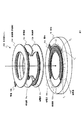
ヘリカル形状をなす多層膜コイルの先行技術としては、例えば特許文献1に開示された小型のチップ状コイルが知られている。図17にそのチップ状コイルの斜視図を示す。導電性薄膜2e,2f,2gが、1層目、2層目、3層目と積層され、コイル端子5aと、ワイヤーボンディング等で接続するパッド端子5bとの間でヘリカルコイルが形成されている。
As a prior art of a multilayer film coil having a helical shape, for example, a small chip coil disclosed in
図18に図17のチップ状コイルの断面図を示す。図18(a)はA−A断面図、図18(b)はB−B断面図である。1はコイル基板であり、1層目の導電性薄膜2eの上に下部絶縁層3aが積層され、その上に2層目の導電性薄膜2fが積層され、その上に上部絶縁層3bが積層され、その上に3層目の導電性薄膜2gが積層されている。そして、最上層には、チップ状コイルの全体を覆うように保護膜7が形成されている。1層目の導電性薄膜2eと2層目の導電性薄膜2fとはスルーホール4aで接続され、2層目と3層目はスルーホール4bで接続される。9a,9b,9cは膜状磁心であり、それぞれの膜状磁心の間には下部絶縁層3aと上部絶縁層3bが介在している。
FIG. 18 is a cross-sectional view of the chip coil shown in FIG. 18A is a cross-sectional view taken along the line AA, and FIG. 18B is a cross-sectional view taken along the line BB.
従来のチップ状コイルは、導電性薄膜間を接続するのに絶縁層に設けたスルーホールを必要としていた。よって、コイルにはスルーホール分の絶縁層の厚みが余分に必要であり、コイルの巻き数を増やすとコイル全体の厚みが厚くなる課題がある。また、コイルの中心軸に設けられる磁心が、絶縁層によって分離された膜状磁心であり、作用の強いバルク(bulk)状の磁心を設けることが難しいという課題がある。また、チップ状コイルの作製には、一定の設備と工数を必要とするフォトリソグラフィ技術(以降、フォトリソ工程とも称する)を用いるのでコスト高になる課題がある。 A conventional chip coil requires a through hole provided in an insulating layer to connect between conductive thin films. Therefore, the coil requires an extra thickness of the insulating layer for the through hole, and increasing the number of turns of the coil increases the thickness of the entire coil. Further, the magnetic core provided on the central axis of the coil is a film-shaped magnetic core separated by an insulating layer, and there is a problem that it is difficult to provide a bulky magnetic core having a strong action. In addition, the production of the chip-shaped coil has a problem of high cost because it uses a photolithography technique (hereinafter also referred to as a photolithography process) that requires a certain amount of equipment and man-hours.
この発明は、このような問題点に鑑みてなされたものであり、スルーホールを用いる必要がなく、バルク状の磁心が使え、フォトリソ工程が不要な多層膜コイルとその作製方法を提供することを目的とする。 The present invention has been made in view of such problems, and it is intended to provide a multilayer film coil that does not require the use of a through hole, can use a bulk magnetic core, and does not require a photolithography process, and a method for manufacturing the same. Objective.
この発明の多層膜コイルは、基板上に導電膜のパターンと絶縁膜のパターンとが交互に積層され、その導電膜のパターン同士が接続されたヘリカル形状である。そのヘリカル形状の軸回りの一周分の周長をPとするとき、導電膜のパターンと絶縁膜のパターンとは周長Pよりも短い定まった周沿いの長さLc,Liを有する。そして、基板上の最下層である場合を除き、ヘリカル形状の軸回りの同一向きについて、絶縁膜のパターンの開始の端点はその直下の導電膜のパターンの開始の端点よりも周沿いの長さP−Liだけ進んだ位置に整合され、導電膜のパターンの開始の端点はその直下の絶縁膜のパターンの開始の端点よりも周沿いの長さP−Lcだけ進んだ位置に整合されてそれぞれ積層され、Li+Lc>Pである。 The multilayer coil according to the present invention has a helical shape in which conductive film patterns and insulating film patterns are alternately stacked on a substrate, and the conductive film patterns are connected to each other. When the circumferential length of one circumference around the helical axis is P, the conductive film pattern and the insulating film pattern have lengths Lc and Li along the circumference which are shorter than the circumferential length P. And, except for the lowermost layer on the substrate, for the same orientation around the axis of the helical shape, the starting end point of the insulating film pattern is longer in the circumference than the starting end point of the conductive film pattern immediately below it The start point of the conductive film pattern is aligned with the position advanced by P-Li, and the start end point of the conductive film pattern is aligned with the position advanced by the length P-Lc along the circumference from the start point of the insulating film pattern immediately below it. Laminated and Li + Lc> P.
この発明によれば、軸回りの定まった同一向きについて、「絶縁膜のパターンの開始の端点は、その直下の導電膜のパターンの開始の端点よりも周沿いの長さP−Liだけ進んだ位置に整合され」る要件によって、絶縁膜のパターンとその直下の導電膜のパターンとを合わせた長さが周長Pに等しくなるため、絶縁膜のパターンの終末の端点は、必ず直下の導電膜のパターンの開始の端点にちょうど突き当たって終端する構成となる。同じく「導電膜のパターンの開始の端点はその直下の絶縁膜のパターンの開始の端点よりも周沿いの長さP−Lcだけ進んだ位置に整合され」る要件によって、導電膜のパターンとその直下の絶縁膜のパターンとを合わせた長さが周長Pに等しくなるため、導電膜のパターンの終末の端点は、必ず直下の絶縁膜のパターンの開始の端点にちょうど突き当たって終端する構成となる。 According to the present invention, “the end point of the insulating film pattern has advanced by a length P-Li along the circumference from the starting end point of the pattern of the conductive film immediately below it in the same direction around the axis. The total length of the insulating film pattern and the conductive film pattern immediately below it is equal to the circumferential length P due to the requirement of “aligned to the position”. It is configured to end just by hitting the starting end point of the film pattern. Similarly, according to the requirement that “the end point of the conductive film pattern is aligned at a position advanced by a length P-Lc along the circumference from the start end point of the insulating film pattern immediately below the conductive film pattern” Since the combined length of the pattern of the insulating film immediately below is equal to the circumferential length P, the end point of the end of the pattern of the conductive film always ends by directly abutting the end point of the pattern of the insulating film immediately below. Become.
このように構成されることによって、この発明の多層膜コイルは、パターンどうしの無駄な重畳部分や間隙が形成されず、従って不要の凹凸もない、膜のパターンが最密に充填され最適にコンパクトで滑らかな交互積層が可能となる。そして、Lc,LiがPよりも短いこととLi+Lc>Pであることとの要件によって、導電膜のパターンの直上の絶縁膜のパターンで覆われない露出部分の形成と、その露出部分における次の導電膜のパターンとの接続とが担保され、コイルが形成される。すなわち、絶縁膜を間に挟んだ導電膜はP−Li>0の長さ分絶縁膜を挟まずに直接重なり合う。この重なり部分で導電膜同士の導通が得られるので、従来技術のようにスルーホールを必要としない。また、それぞれ定まった形状の導電膜のパターンと絶縁膜のパターンを交互に積層する構造なので、フォトリソ工程を用いずに、メカマスクの利用によって、コイルの形態によってはたかだか2枚或いはたった1枚のメカマスクの利用によって、簡便な成膜工程で導電膜と絶縁膜とを交互積層してコイルを形成することが可能である。 By being configured in this way, the multilayer coil of the present invention does not form useless overlapping portions or gaps between patterns, and therefore there is no unnecessary unevenness, and the film pattern is closely packed and optimally compact And smooth alternating lamination becomes possible. Then, depending on the requirement that Lc and Li are shorter than P and Li + Lc> P, formation of an exposed portion that is not covered with the pattern of the insulating film immediately above the pattern of the conductive film, and the next in the exposed portion Connection with the pattern of the conductive film is secured, and a coil is formed. That is, the conductive films sandwiching the insulating film directly overlap each other without the insulating film being sandwiched by the length of P-Li> 0. Since conduction between the conductive films can be obtained at the overlapping portion, a through hole is not required unlike the prior art. In addition, since the structure of the conductive film and the pattern of the insulating film, each having a predetermined shape, are alternately laminated, the mechanical mask is used without using the photolithography process, and at most two or only one mechanical mask depending on the form of the coil. By using this, it is possible to form a coil by alternately laminating conductive films and insulating films by a simple film forming process.
以下、この発明の実施の形態を図面を参照して説明する。複数の図面中同一のものには同じ参照符号を付し、説明は繰り返さない。 Embodiments of the present invention will be described below with reference to the drawings. The same reference numerals are given to the same components in a plurality of drawings, and the description will not be repeated.
図1にこの発明の多層膜コイル200の構造例を斜視図で示す。非導電性の例えばガラス材で構成される高さの低い円柱状の基板10の上に、周沿いの長さP−Lcの円弧が切り欠かれた円環形状の周沿いの長さLcの導電膜のパターン14aが、切り欠かれたP−Lcの部分を右向き(図1において)にして成膜されている。Pはヘリカル形状の円をなす軸回りの一周分の周長であり、LcはPより小とされる。この例では、絶縁膜のパターン12aは、導電膜のパターン14aよりもやや幅広である。絶縁膜のパターン12aは、導電膜のパターン14aの上(基板10と反対側)に、図中の矢印の向きに見下ろして時計回りとなる向きに、端点T2から周沿いの長さLiだけ成膜されている。開始の端点T2は、基板10の上側から見て、導電膜のパターン14aの開始の端点T1よりも時計回りに周沿いの長さP−Liだけ進んだ位置である。ここで、LiもPより小とされ、またLi+Lc>Pである。なお、図1においては、P、Lc、Liは円環形状の外周の長さを示している。しかし、これに限る必要はなく、あらかじめ定めておけば、円環形状のどの部分の長さでもかまわない。例えば、内周の長さや中心の長さでもかまわない。
FIG. 1 is a perspective view showing an example of the structure of a multilayer film coil 200 of the present invention. On a cylindrical substrate 10 having a low height and made of a non-conductive glass material, for example, a circular arc having a length P-Lc along the circumference is cut out and the length Lc along the circumference of the annular shape is cut. A
このようにすれば、導電膜のパターン14aとその直上の絶縁膜のパターン12aとを合わせた周沿いの長さがちょうど周長Pに等しくなるので、絶縁膜のパターン12aの終端の端点T3は、導電膜のパターン14aの開始の端点T1にちょうど突き当たる。したがって、端点T1と端点T3の間に無駄な空隙や重畳が形成されず、この両端点の突き当たりの部分において導電膜のパターン14aと絶縁膜のパターン12aとは滑らかに接続する。そしてその両端点の突き当たりの部分の上に成膜されるパターン、この例では導電膜のパターン14bを、その無駄な空隙や重畳による凹凸の無い下層の上に滑らかに形成することができる。なお、この例では、導電膜のパターン14aの終端の近傍に電極16aが成膜される例を示している。
In this way, the length along the circumference of the
そして次に、第3層目となる導電膜のパターン14bが、その直下の絶縁膜のパターン12aの開始の端点T2よりも時計回りに周沿いの長さP−Lc進んだ位置を開始の端点として成膜され、同様にその導電膜のパターン14bの終端の端点が絶縁膜のパターン12aの開始の端点T2に突き当たる。ここで第1層目の導電膜のパターン14aの露出していた長さP−Liの円弧部分の表面において、その第1層目の導電膜のパターン14aと第3層目の導電膜のパターン14bとが直接に接続する。以降同様にして絶縁膜のパターンと導電膜のパターンとの交互積層を繰り返し、この例では第7層目の導電膜のパターン14dに他方の電極16bが形成され、その上には保護膜を兼ねた絶縁膜のパターン12dが成膜されてヘリカル形状の多層膜コイル200が、電極16aと16b間に形成されている。
And then, the
このようにして、最適にコンパクトな多層膜コイルが構成される。なおこの実施例1において、LcとLiとは互いに等しい長さである必要はない。またこの例では、導電膜間の短絡防止を強化するために、絶縁膜のパターン12a〜12dを導電膜のパターン14a〜14dよりもやや幅広としているが、これらを同一の幅で形成してもよい。
In this way, an optimally compact multilayer coil is constructed. In Example 1, Lc and Li need not have the same length. In this example, the insulating
さらに、この例では導電膜のパターンと絶縁膜のパターンとに円環形状を用いたが、本発明においてコイルのヘリカル形状は、軸に垂直な平面への射影が正円となる線形状を描くものに限らない。実施例1の変形例として、非正円や多角形を含む周長がPの周回形状を繰り返すヘリカル形状のコイルが、実施例1と同様に構成され得る。
〔多層膜コイル200の作製方法〕
次に、図1に示した多層膜コイル200の作製方法を説明する。
Furthermore, in this example, an annular shape is used for the conductive film pattern and the insulating film pattern. However, in the present invention, the helical shape of the coil draws a linear shape whose projection onto a plane perpendicular to the axis is a perfect circle. Not limited to things. As a modified example of the first embodiment, a helical coil that repeats a circular shape having a circumference including a non-circular circle or a polygon may be configured in the same manner as in the first embodiment.
[Method for Manufacturing Multilayer Coil 200]
Next, a method for manufacturing the multilayer coil coil 200 shown in FIG. 1 will be described.
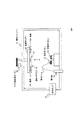
図2に、導電膜のパターン14を成膜する導電成膜マスク20の一例と、絶縁膜のパターン12を成膜する絶縁成膜マスク25の一例を示す。図2(a)は導電膜のパターン14を成膜する導電成膜マスク20の一例、図2(b)は絶縁膜のパターン12を成膜する絶縁成膜マスク25の一例である。この導電成膜マスク20と絶縁成膜マスク25は、例えばステンレス等の金属円板で構成されるメカマスクであり、成膜の工程において、図3に示すように基板10の表面にほぼ接するように位置決めされる。 FIG. 2 shows an example of a conductive film forming mask 20 for forming the conductive film pattern 14 and an example of an insulating film forming mask 25 for forming the insulating film pattern 12. 2A shows an example of a conductive film forming mask 20 for forming a conductive film pattern 14, and FIG. 2B shows an example of an insulating film forming mask 25 for forming an insulating film pattern 12. The conductive film forming mask 20 and the insulating film forming mask 25 are mechanical masks made of, for example, a metal disk such as stainless steel, and are substantially in contact with the surface of the substrate 10 as shown in FIG. Positioned.
導電成膜マスク20と絶縁成膜マスク25とは、それぞれ、図1の多層膜コイル200の導電膜のパターン14、絶縁膜のパターン12に各一致する導電膜のパターンの開口部21、絶縁膜のパターンの開口部26を有している。すなわち、導電膜のパターンの開口部21は、図2(a)に示すように、周長Pの円環から周沿いの長さP−Lcの円弧を切り欠いた周沿いの長さLcの円環形状を有している。また絶縁膜のパターンの開口部26は、図2(b)に示すように、周長Pの円環から周沿いの長さP−Liの円弧を切り欠いた周沿いの長さLiの円環形状を有している。そして絶縁膜のパターンの開口部26は、導電膜のパターンの開口部21よりもやや幅広とされている。 The conductive film formation mask 20 and the insulation film formation mask 25 are respectively the conductive film pattern 14 of the multilayer coil 200 of FIG. 1, the conductive film pattern opening 21 corresponding to the insulation film pattern 12, and the insulation film. The opening 26 of the pattern is provided. That is, as shown in FIG. 2A, the opening 21 of the conductive film pattern has a length Lc along the circumference obtained by cutting out a circular arc having a length P-Lc along the circumference from a ring with a circumference P. It has an annular shape. Further, as shown in FIG. 2B, the opening 26 of the pattern of the insulating film is a circle having a length Li along the circumference obtained by cutting out an arc having a length P-Li along the circumference from a ring having a circumference P. It has a ring shape. The opening 26 of the insulating film pattern is slightly wider than the opening 21 of the conductive film pattern.
導電膜と絶縁膜のパターンは一般的な蒸着法若しくはスパッタ法によって成膜される。図3に真空蒸着法で用いる蒸着装置の概略図を示して薄膜形成方法を説明する。真空チャンバー40内は、排気ポンプ42によって例えば10−4Pa以下の高真空に保たれる。熱源としての電子銃41は、導電膜の蒸着源43と絶縁膜の蒸着源44を、それぞれの成膜時に蒸発させる。導電膜の蒸着源43は例えばCu、絶縁膜の蒸着源44は例えばSiO2等が用いられる。
The pattern of the conductive film and the insulating film is formed by a general vapor deposition method or a sputtering method. FIG. 3 shows a schematic diagram of a vapor deposition apparatus used in the vacuum vapor deposition method, and the thin film formation method will be described. The inside of the vacuum chamber 40 is maintained at a high vacuum of, for example, 10 −4 Pa or less by the
対向する位置に基板ホルダー48と基板10が配置され、その上に導電成膜マスク20または絶縁成膜マスク25が、基板10の表面にほぼ接するように位置決めされる。ここで導電成膜マスク20と絶縁成膜マスク25とは、基板10上に交互に取り換え設置され、導電成膜マスク20が設置される時に導電膜の蒸着源43が、絶縁成膜マスク25が設置される時に絶縁膜の蒸着源44が、それぞれ電子銃41によって蒸着される。その取り換え設置の際、軸回りの同一の向きについて、絶縁成膜マスク25のその向きに関する絶縁膜のパターンの開口部26の始まりの端点は、その直前に設置された導電成膜マスク20のその向きに関する導電膜のパターンの開口部21の始まりの端点の位置よりも、その向きについて周沿いにP−Liだけ進んだ位置に来るように位置合わせされる。同じく、導電成膜マスク20のその向きに関する導電膜のパターンの開口部21の始まりの端点は、その直前に設置された絶縁成膜マスク25のその向きに関する絶縁膜のパターンの開口部26の始まりの端点の位置よりも、その向きについて周沿いにP−Lcだけ進んだ位置に来るように位置合わせされる。
The substrate holder 48 and the substrate 10 are disposed at opposite positions, and the conductive film formation mask 20 or the insulation film formation mask 25 is positioned on the substrate holder 48 and the substrate 10 so as to be substantially in contact with the surface of the substrate 10. Here, the conductive film formation mask 20 and the insulation film formation mask 25 are alternately installed on the substrate 10. When the conductive film formation mask 20 is installed, the conductive film deposition source 43 is replaced by the insulation film formation mask 25. When installed, an insulating film deposition source 44 is deposited by each
このようにして、2枚のメカマスクを交互に、軸回りに方位をずらしつつ設置して成膜してゆくことで、図1の多層膜コイル200を積層してゆくことができる。 Thus, the multilayer film coil 200 of FIG. 1 can be laminated | stacked by carrying out film-forming by installing two mechanical masks alternately, shifting an azimuth | direction around an axis | shaft.
また変形例として、導電膜のパターン及び絶縁膜のパターンが正多角形からそれぞれ1辺ないし連続する複数の辺を切り欠いて得る形状を有するようなコイルであっても、全く同様に2枚のメカマスクを軸回りにずらしながら交互に設置して成膜してゆくことができる。或いは、導電膜のパターンと絶縁膜のパターンとを長さ及び幅に関して全く同じ形状とし、たった1枚のメカマスクをその両方に共用して軸回りに方位をずらしながら交互に成膜を行い、コイルを作製することもできる。その他、垂直断面への射影が正円や正多角形でないようなヘリカル形状の多層膜コイルも、導電膜及び絶縁膜のパターンのためにそれぞれ必要な数だけのメカマスクを用意して、成膜し積層してゆくことができる。 As a modification, even if the conductive film pattern and the insulating film pattern have a shape obtained by cutting out one side or a plurality of continuous sides from a regular polygon, two coils are exactly the same. The mechanical masks can be alternately installed while being shifted around the axis to form a film. Alternatively, the pattern of the conductive film and the pattern of the insulating film are made the same in terms of length and width, and only one mechanical mask is shared by both, and the film is alternately formed while shifting the direction around the axis. Can also be produced. In addition, a helical multilayer coil whose projection on the vertical cross section is not a perfect circle or regular polygon is also prepared by preparing as many mechanical masks as necessary for the conductive film and insulating film patterns. Can be stacked.
以上は最も一般的な場合であるが、これに対して特に、コイルのヘリカル形状が断面正円(半径R)であり、導電膜のパターンと絶縁膜のパターンとが共に、kをk≧3の整数として The above is the most general case, but in particular, the helical shape of the coil is a perfect circle (radius R), and k is k ≧ 3 for both the conductive film pattern and the insulating film pattern. As an integer

と書けるような中心角Φをもつ円弧状とすればさらに作製の容易がはかれる。すなわちこの場合には、実施例1の2枚のメカマスクに替えて、導電膜のパターンの開口部と絶縁膜のパターンの開口部との両方を形成した1枚の回転メカマスクを利用し、それを真空チャンバー内で回動させながら交互の成膜を行ってゆくことで、メカマスクの取り換え設置をせずに、しかも複数個の多層膜コイルを同時に並行して、効率的に作製できる。以下、この例について詳細に説明する。 If the arc shape has a central angle Φ that can be written as follows, the fabrication is further facilitated. That is, in this case, instead of the two mechanical masks of the first embodiment, a single rotating mechanical mask in which both the opening of the conductive film pattern and the opening of the insulating film pattern are formed is used. By alternately forming the films while rotating in the vacuum chamber, a plurality of multilayer coils can be efficiently manufactured in parallel without replacing the mechanical mask. Hereinafter, this example will be described in detail.
図4に、回転メカマスクを用いる蒸着装置の概略図を示す。蒸着源43、44に対向する位置に基板ホルダー48と複数の被膜基板(図示の例では、基板10aと10b)と回転メカマスク45が配置される。被膜基板は上記した基板10(図1)と同じものであり、蒸着源43,44側の面を被膜面として基板ホルダー48に固定されている。その被膜基板の被膜面に近接して回転メカマスク45が配置されている。
FIG. 4 shows a schematic view of a vapor deposition apparatus using a rotating mechanical mask. A substrate holder 48, a plurality of coated substrates (
回転メカマスク45が回転モーター49によって回転されることで、それぞれの被膜基板の上に位置する導電膜のパターンの開口部と絶縁膜のパターンの開口部とが切り替わる。被膜基板(すべて)の被膜面の上に導電膜のパターンの開口部が配置された時は、蒸着源43が電子銃41によって蒸発され、被膜基板の被膜面に導電膜(例えばCu)のパターンが成膜される。絶縁膜のパターンを成膜する時には、被膜基板の被膜面の上に絶縁膜のパターンの開口部が配置され蒸着源44が蒸発されて、絶縁膜(例えばSiO2)のパターンが成膜される。
When the rotary mechanical mask 45 is rotated by the
回転メカマスクには、その回転軸からの方位につき上記(1)式のαに等しい角度ごとの間隔をあけ、かつ、パターンの円環形状の中心が回転軸の周りの同一半径Rmの周上となるように、全部でk個の導電膜または絶縁膜のパターンの開口部を設ける。 The rotating mechanical mask is spaced at an angle equal to α in the equation (1) with respect to the direction from the rotation axis, and the center of the ring shape of the pattern is on the circumference of the same radius Rm around the rotation axis. Thus, a total of k conductive film or insulating film pattern openings are provided.
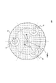
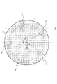
このような回転メカマスクを利用して作製できる多層膜コイルの例として、まず、導電膜のパターンと絶縁膜のパターンとがともに中心角Φ=270°の円弧状である多層膜コイルについて説明する。この場合、上記(1)式のα=90°、整数k=4である。図5に、図4に示す矢印A方向から見たこの例の多層膜コイルを作製するための回転メカマスク45と基板ホルダー48を示す。図5(a)が回転メカマスク45の形状を示す図であり、図5(b)が基板ホルダー48と基板10a、10bの配置を示す図である。回転メカマスク45には、回転軸(原点)47を中心とした所定の半径Rmの円周上に、中心角α=90°分の弧を切り欠いた円環形状の導電膜のパターンの開口部45aと45bと、絶縁膜のパターンの開口部46aと46bとが、2個ずつ合わせて計4個、全て同一の向きに、パターンの切り欠きの中心角と等しい角度すなわちα=90°ごとの間隔を空けた方位に、交互に設けられる。
As an example of a multilayer coil that can be manufactured using such a rotating mechanical mask, a multilayer coil in which the conductive film pattern and the insulating film pattern are both arcs with a central angle Φ = 270 ° will be described first. In this case, α = 90 ° and integer k = 4 in the above equation (1). FIG. 5 shows a rotating mechanical mask 45 and a substrate holder 48 for manufacturing the multilayer film coil of this example as seen from the direction of arrow A shown in FIG. FIG. 5A is a diagram showing the shape of the rotating mechanical mask 45, and FIG. 5B is a diagram showing the arrangement of the substrate holder 48 and the
2つの被膜基板である基板10aと基板10bは、例えば図5(a)の導電膜のパターンの開口部45a,45bの位置に同時に整合することができるように配置される。つまり、回転メカマスク45の導電膜のパターンの開口部45a,45b又は絶縁膜のパターンの開口部46a,46bの何れか一方の種類の開口部に対応する位置に、基板ホルダー48上に図5(b)に例示するように配置される(配置する基板は、もちろん何れか一方のみでもよい。)。
The two coated substrates, the substrate 10a and the
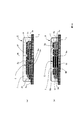
図6に、導電膜のパターン14と絶縁膜のパターン12を交互に成膜する工程を示す。図6(a)は、図5(b)に示した基板10aの上に電極16a付きの導電膜のパターン14aが成膜された状態を示す。なお、説明は基板10a上の薄膜形成について説明するが、回転メカマスク45を用いて図5(b)に示したように基板ホルダー48の上に基板10bも配置すると、基板10bの上にも同じ薄膜が同時に成膜されることになる。
FIG. 6 shows a process of alternately forming the conductive film pattern 14 and the insulating film pattern 12. FIG. 6A shows a state in which a
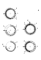
図6(a)の導電膜のパターン14aは、図5(a)に示した位置の回転メカマスク45を反時計方向(矢印Aの方向から見て)に90°回転させて、導電膜のパターンの開口部45aを、基板10aの上に位置決めして成膜されたものである。電極16aは、予め図示しない電極形成用のマスクによって成膜される。
The
図6(b)に示す絶縁膜のパターン12aは、図6(a)の導電膜のパターン14aを成膜した時の回転メカマスク45を、時計方向に90°回転させて導電膜のパターン14aの上に成膜された絶縁膜である。この時、絶縁膜のパターン12aは、導電膜のパターン14aの開始の端点よりも、時計方向に周沿いの長さP−Liの長さ進んだ位置から成膜される。なお、図6を用いた説明では、円環形状の中心部分の周沿いの長さを、単に周沿いの長さと言うことにする。
The insulating
図6(c)に示す導電膜のパターン14bは、更に回転メカマスク45を時計方向に90°回転させ、基板10aの位置に導電膜のパターンの開口部45bを位置決めして成膜された導電膜である。この時、導電膜のパターン14bは、絶縁膜のパターン12aの開始の端点よりも、時計方向に周沿いの長さP−Lcの長さ進んだ位置から成膜され、一層前の導電膜のパターン14aと斜線で示す部分で導通する。
The
図6(d)に示す絶縁膜のパターン12bは、更に回転メカマスク45を時計方向に90°回転させ、導電膜のパターン14bの開始の端点よりも、時計方向に周沿いの長さP−Li進んだ位置から成膜される。
In the insulating
図6(e)に示す導電膜のパターン14cは、更に回転メカマスク45を時計方向に90°回転させ、絶縁膜のパターン12bの開始の端点よりも、時計方向に周沿いの長さP−Lc進んだ位置から成膜される。そして、図示しない電極形成用のマスクによって電極16bが形成される。導電膜のパターン14cは、一層前の導電膜のパターン14bと斜線で示す部分で導通する。
[変形例1]
以上は整数k=4の場合の例を述べたが、一般に、kを偶数とすると、回転メカマスクに、回転軸からの方位につき角度α=360°/kごとの間隔をあけて交互に、導電膜のパターンの開口部と絶縁膜のパターンの開口部とをk/2個ずつ設けることで、何れか一方の種類の開口部に対応する位置に1個以上k/2個以下の数だけ被膜基板を配置して成膜することができる。よって、kが偶数の場合は、両者のパターンの形状を変えることが可能である。したがって、kが偶数の場合は、図5(a)に示すように導電膜のパターンの開口部45a,45bの幅を、絶縁膜のパターンの開口部46a,46bの幅よりも狭くすると好都合である。その方が、積層される導電膜のパターン同士の短絡を発生し難くすることができる。
In the
[Modification 1]
Although the example in the case of the integer k = 4 has been described above, in general, when k is an even number, the rotating mechanical mask is alternately conductive at intervals of an angle α = 360 ° / k per direction from the rotation axis. By providing k / 2 openings for the pattern of the film and openings for the pattern of the insulating film, the number of the coatings is one or more and no more than k / 2 at the position corresponding to one of the openings. A substrate can be placed to form a film. Therefore, when k is an even number, it is possible to change the shapes of both patterns. Therefore, when k is an even number, it is advantageous to make the widths of the
絶縁膜のパターンと導電膜のパターンの周沿いの長さLi,Lcは、上記して説明した例に限定されない。その長さは任意の長さに設定することが可能である。図7に、弧の長さP−Li若しくはP−Lcを決める中心角αをα=30°とした場合の回転メカマスク70の平面図を示す。 The lengths Li and Lc along the circumference of the insulating film pattern and the conductive film pattern are not limited to the example described above. The length can be set to an arbitrary length. FIG. 7 shows a plan view of the rotating mechanical mask 70 when the central angle α for determining the arc length P-Li or P-Lc is α = 30 °.
回転メカマスク70には、回転軸(原点)76を中心とした所定の半径Rmの円周上に、中心角α=30°に対する弧の長さP−Lcが切り欠かれた周沿いの長さがLcの円環形状の導電膜のパターンの開口部70a〜70fと、周沿いの長さがLiの絶縁膜のパターンの開口部71a〜71fとが6個ずつ合わせて計12個(k=12)、全て同一の向きに30°の角度毎に交互に配置される。なお、図7では、導電膜のパターンの開口部70a〜70fを灰色、絶縁膜のパターンの開口部71a〜71fを白抜きで示している。
The rotating mechanical mask 70 has a length along the circumference in which the arc length P-Lc with respect to the central angle α = 30 ° is cut out on the circumference having a predetermined radius Rm with the rotation axis (origin) 76 as the center. A total of 12
回転メカマスク70の導電膜のパターンの開口部又は絶縁膜のパターンの開口部の何れか一方の種類の開口部に対応する位置に1個以上k/2個以下の被膜基板を配置し、被膜基板の上に導電膜のパターン又は絶縁膜のパターンの一方を成膜し、回転メカマスクを回転軸76を中心に同一の向きに中心角α分の角度を回転させて導電膜のパターンと絶縁膜のパターンとを交互に積層して多層膜コイルを作製する。
One or more k / 2 or less coated substrates are arranged at positions corresponding to any one of the openings of the conductive film pattern or the insulating film pattern of the rotating mechanical mask 70, and the coated substrate One of the conductive film pattern and the insulating film pattern is formed on the substrate, and the rotating mechanical mask is rotated about the
以上、k=4とk=12の例を示したが、kが偶数であれば同様にしてk/2個の多層膜コイルを同時に作製できる。
[変形例2]
実施例1、実施例2、実施例2変形例1では、絶縁膜のパターンは導電膜のパターンよりも幅広であった。しかし、導電膜のパターンと絶縁膜のパターンは、同一形状にしても良い。図8に中心角Φ=300°、α=60°に対する弧の長さが切り欠かれた導電膜のパターンと絶縁膜のパターンとが同一形状の回転メカマスク80を示す。回転メカマスク80は、開口部のパターンが同一なので、導電膜のパターンの開口部と絶縁膜のパターンの開口部とは共通であって区別はなく、それらの開口部に対応する位置に1個以上最大k=6個までの数の被膜基板を配置して、回転メカマスクをα=60°ずつ回転させ導電膜と絶縁膜とを交互に成膜してゆくことができる。
The example in which k = 4 and k = 12 has been described above. However, if k is an even number, k / 2 multilayer coils can be manufactured at the same time.
[Modification 2]
Example 1, Example 2, Example 2 In
実施例2ではkを偶数とした場合を示したが、kを奇数としてもよい。図9に、k=3(α=120°)としたときの回転メカマスク90の平面図を示す。
In the second embodiment, k is an even number, but k may be an odd number. FIG. 9 shows a plan view of the rotating
kが奇数の場合は、導電膜のパターンの開口部と絶縁膜のパターンの開口部を、回転メカマスク90の全周に渡って交互に設けることができない。つまりkが奇数の時は、導電膜のパターンの開口部と絶縁膜のパターンの開口部とは共通の形状とされ、(上述の実施例2変形例2と同じく)開口部は共通で利用される。例えばk=3の場合、開口部91,92,93は、回転軸(原点)96を中心とした所定の半径Rmの円周上にα=120°毎に同一の向きに設けられる。ここで、被膜基板は、全ての開口部に対応する基板ホルダー48上に配置することが可能である。つまり、回転メカマスク90を用いる際の被膜基板は、何れかの開口部に対応する位置に1個以上k個以下の数、配置される。図9の場合、被膜基板は最大3個配置することができる。
When k is an odd number, the opening of the conductive film pattern and the opening of the insulating film pattern cannot be alternately provided over the entire circumference of the rotating
回転メカマスク90を使用して絶縁膜のパターンと導電膜のパターンを成膜する工程は、各膜を成膜する度に回転メカマスク90を回転させる角度が120度である点が異なるだけで、図6で説明した工程と全く同じである。なお、3以外の奇数5、7、9、11でも同様である。
The process of forming the insulating film pattern and the conductive film pattern using the rotating
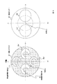
実施例2と実施例3とでは、絶縁膜のパターンと導電膜のパターンの形状が円環形状の場合について説明した。しかし、その形状はN≧3(Nは整数)の正N角形でもよい。その場合は、mを1≦m<N/2である整数として、その正N角形から連続したm個の辺を切り欠いた形状で導電膜及び絶縁膜のパターンを構成する。すなわち上述の導電膜及び絶縁膜のパターンの長さLc及びLiは、ともに正N角形の連続したN−m個の辺の長さ分に相当し、ここでm<N/2とするのは、上述の実施例1に関して述べた一般的な条件Li+Lc>Pを担保するためである。図10に、N=4、正四角形とした場合の回転メカマスク100を示す。上記不等式の条件から、今の場合は必然的にm=1である。従って、回転メカマスク100には、回転軸(原点)106を中心とした所定の半径Rmの円周上に、中心角α’=360°/(N/m)=360°/k’=90°毎に(k’=N/mについては後述する。)一辺が切り欠かれた正四角形(カタカナの「コ」を左右反対にした形)の導電膜のパターンの開口部101aと101bと、絶縁膜のパターンの開口部102aと102bとが2個ずつ合わせて計4個、全て同一の向きに90度の角度毎に交互に設けられる。
In Example 2 and Example 3, the case where the shape of the pattern of the insulating film and the pattern of the conductive film is an annular shape has been described. However, the shape may be a regular N-gon with N ≧ 3 (N is an integer). In that case, m is an integer satisfying 1 ≦ m <N / 2, and the pattern of the conductive film and the insulating film is formed in a shape in which m sides continuous from the regular N-gon are notched. That is, the lengths Lc and Li of the conductive film and insulating film patterns described above correspond to the length of N−m continuous sides of a regular N-gon, where m <N / 2. This is to ensure the general condition Li + Lc> P described in connection with the first embodiment. FIG. 10 shows the rotating
切り欠かれた辺の数をmとすると、図10において、導電膜のパターンの開口部101a,101bと、絶縁膜のパターンの開口部102a,102bはN−m=4−1=3個の辺の連続した形状であり、上記したLiとLcに相当する長さは3個の辺の連続した長さである。ここで一般に、mを、k′=N/mが偶数(今の場合はk’=4/1=4)となるNの約数とすれば、導電膜のパターンの開口部と絶縁膜のパターンの開口部との形状を変えることが可能である。すなわち図10の例においては、絶縁膜のパターンの開口部102a,102bと、導電膜のパターンの開口部101a,101bの形状を変えることが可能である。そして、絶縁膜のパターンの開口部102a,102bを、導電膜のパターンの開口部101a,101bよりも相対的に幅広の形状にすることが可能であり、それによって積層される導電膜のパターン同士の短絡を発生し難くすることができる。
[変形例]
これに対し、k’=N/mが奇数となる場合について次に述べる。図11に、回転メカマスク100の変形例として正六角形(N=6)でm=2とした回転メカマスク110の例を示す。この例では、k’=N/m=3である。回転メカマスク110には、回転軸116を中心とした所定の半径Rmの円周上に、中心角α′=120°毎に2辺が切り欠かれた正六角形の開口部111〜113が3個、全て同一の向きに120°の角度毎に設けられる。k’が奇数の場合は、実施例3で説明した同じ理由で、絶縁膜のパターンの開口部と導電膜のパターンの開口部は、共通の形状とされる。
Assuming that the number of cut-out sides is m, in FIG. 10, the
[Modification]
On the other hand, the case where k ′ = N / m is an odd number will be described next. FIG. 11 shows an example of a rotating
一般に、k’が奇数の場合には、回転メカマスク(110)の開口部に対応する位置に1個以上N個以下の被膜基板を配置し、その被膜基板の上に導電膜のパターン又は絶縁膜のパターンの一方を成膜する。そして、回転メカマスク(110)を、回転軸(原点)(116)を中心に同一の向きに中心角α′分回転させて導電膜のパターンと絶縁膜のパターンとを交互に積層して多層膜コイルを作製する。 Generally, when k ′ is an odd number, one or more and N or less coated substrates are arranged at positions corresponding to the openings of the rotating mechanical mask (110), and a conductive film pattern or insulating film is formed on the coated substrate. One of the patterns is formed. Then, the rotating mechanical mask (110) is rotated about the rotation axis (origin) (116) in the same direction by the central angle α ′, and the conductive film pattern and the insulating film pattern are alternately laminated to form a multilayer film. A coil is produced.
同じくk’が奇数となる場合のもう1つの例として、図12に正五角形(N=5)でm=1とした回転メカマスク120の例を示す。回転メカマスク120には、回転軸126を中心とした所定の半径Rmの円周上に、中心角α′=72°(360°/N)毎に1辺が切り欠かれた正五角形の開口部121〜125が5個、全て同一の向きに72°の角度毎に設けられる。
Similarly, as another example in the case where k ′ is an odd number, FIG. 12 shows an example of a rotating
絶縁膜のパターンの開口部と導電膜のパターンの開口部は共通の形状とされる点、及び、回転メカマスク120を、回転軸(原点)126を中心に同一の向きに中心角α′分の角度を回転させて、それぞれの膜を成膜する作製方法は実施例4変形例と同じである。
The opening portion of the insulating film pattern and the opening portion of the conductive film pattern have a common shape, and the rotating
以上は、図10〜図12に示す例を参照して、k’=N/mが偶数または奇数となる、すなわちmがNの約数となるように選んだ場合について述べた。 The case where k ′ = N / m is selected to be an even number or an odd number, that is, m is a divisor of N has been described above with reference to the examples illustrated in FIGS.
しかし、mがNの約数でない、すなわちk’=N/mが(偶数または奇数の)整数とならないような整数の組Nとmを選んでも、やはり回転メカマスクを利用して本発明を実施することは可能である。そのような場合には、回転メカマスクに回転軸からの方位につき角度360°/Nごとの間隔をあけて、導電膜のパターンと絶縁膜のパターンとに共通する開口部をN個、全て同一の向きに配置して設け、それらの開口部に対応する位置に1個以上N個以下の被膜基板を固定して、回転メカマスクを回転軸周りに360°・m/Nに等しい角度ずつ回転しながら導電膜と絶縁膜とを交互に成膜してゆけばよい。 However, even if an integer set N and m is selected such that m is not a divisor of N, that is, k ′ = N / m is not an integer (even or odd), the present invention is still implemented using a rotating mechanical mask. It is possible to do. In such a case, the opening is common to the pattern of the conductive film and the pattern of the insulating film at an angle of 360 ° / N with respect to the direction from the rotation axis in the rotating mechanical mask. 1 or more and N or less coated substrates are fixed at positions corresponding to the openings, and the rotating mechanical mask is rotated around the rotation axis by an angle equal to 360 ° · m / N. A conductive film and an insulating film may be alternately formed.
図13に、N=5、m=2とした回転メカマスク130の例を示す。回転メカマスク130には、回転軸136を中心とした所定の半径Rmの円周上に、2辺が切り欠かれた正五角形の開口部131〜135が5個、全て同一の向きに360°/N=360°/5=72°の角度毎に設けられる。そして、その72°の2倍の角度すなわち144°に等しい角度ずつ回転させて導電膜と絶縁膜とを交互に成膜・積層することで左巻きに導電パターンがつながり、コイルが形成できる。
FIG. 13 shows an example of the rotating
このコイル形成の様子を図14に示す。図14(a)は、図13の開口部131に対応する位置に被膜基板を配置して導電膜のパターンe1,d1,c1を形成した状態を示している。図14(b)は、回転メカマスク130を時計方向に360°・2/5=144°回転させ開口部134が被膜基板の上になる状態で絶縁膜のパターンb1,a1,e2を成膜した状態を示す。導電膜のパターンe1の上に絶縁膜のパターンe2が成膜される。
The state of this coil formation is shown in FIG. FIG. 14A shows a state in which the conductive film patterns e 1 , d 1 , and c 1 are formed by disposing a film substrate at a position corresponding to the
図14(c)は、更に回転メカマスク130を時計方向に360°・2/5=144°回転させ開口部132が被膜基板の上になる状態で導電膜のパターンd2,c2,b2を成膜した状態を示す。1層目の導電膜のパターンd1,c1と導通が取れた導電膜のパターンb2が、絶縁膜のパターンb1の上に成膜されてコイルの導線が左巻きの方向で延長されることが分かる。図14(d)は、次の絶縁膜のパターンの成膜工程で、絶縁膜のパターンd3が導電膜のパターンd2の上に延長された状態を示す。図14(e)は、その次の成膜工程で絶縁膜のパターンa2の上に導電膜のパターンa3が成膜された状態を示している。なお、この実施例5について説明したコイルの作成方法、すなわち回転メカマスクを360°・m/Nに等しい角度ずつ回転させながら、導電膜のパターンと絶縁膜のパターンを交互に成膜する方法は、上述のmがNの約数でない場合だけに限定されず、k’=N/mが偶数または奇数である場合にも、導電膜のパターンと絶縁膜のパターンとが同一の形状でさえあれば、より一般的にこれを利用してその正N角形状の多層膜コイルが作製できる。
FIG. 14C shows the conductive film patterns d 2 , c 2 , b 2 in a state in which the rotating
以上説明した例は、図3に示す矢印Aの方向から見て、回転メカマスクを時計方向に中心角α若しくはα′ずつ回転させるごとに、導電膜のパターンと絶縁膜のパターンとを交互に成膜して多層膜コイルを作製する方法である。この作製方法では左巻きの多層膜コイルが作製される。つまり、回転メカマスクの回動方向とコイルの巻き線の方向は逆向きとなる。 In the example described above, the conductive film pattern and the insulating film pattern are alternately formed each time the rotating mechanical mask is rotated clockwise by the central angle α or α ′ as seen from the direction of the arrow A shown in FIG. In this method, a multilayer coil is formed by film formation. In this manufacturing method, a left-handed multilayer coil is manufactured. That is, the rotating direction of the rotating mechanical mask and the winding direction of the coil are opposite to each other.
右巻きの多層膜コイルの作製も同様な方法で作製することが可能である。図15(a)に、右巻きの多層膜コイルを作製する場合の回転メカマスク45′、図15(b)に基板ホルダー48′上の基板10a′,10b′を示す。図15(a)と(b)は、説明済みの図5をY軸(開口部45aと45bの配列方向)対称とした図であり、各参照符号には「′」を付して区別をしているが、開口部の方向が異なるだけで同じ働きをするものである。
The right-handed multilayer coil can be manufactured in the same manner. FIG. 15 (a) shows a rotating mechanical mask 45 ′ for producing a right-handed multilayer coil, and FIG. 15 (b) shows the substrates 10a ′ and 10b ′ on the substrate holder 48 ′. FIGS. 15A and 15B are diagrams in which FIG. 5 described above is symmetric with respect to the Y axis (the direction in which the
回転メカマスク45′を反時計方向に中心角度αずつ回転させながら導電膜のパターンと絶縁膜のパターンとを交互に成膜することで、右巻きの多層膜コイルを作製することができる。その工程は、回転メカマスク45′の回転方向が異なるだけで、図6と同じである。 A right-handed multilayer coil can be produced by alternately forming a conductive film pattern and an insulating film pattern while rotating the rotating mechanical mask 45 ′ counterclockwise by a central angle α. The process is the same as that in FIG. 6 except that the rotation direction of the rotating mechanical mask 45 'is different.
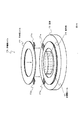
図16に、多層膜コイルのヘリカル形状の軸の位置に一体(バルク状)の磁性体を設けた多層膜コイル170の斜視図を示す。多層膜コイル170は、基板173の上に形成された多層膜コイル171のヘリカル形状の軸の位置に例えばフェライト材料の一体の磁性体174が設けられたものである。
FIG. 16 is a perspective view of a multilayer coil 170 in which an integral (bulk) magnetic body is provided at the position of the helical axis of the multilayer coil. The multilayer coil 170 is obtained by providing an integral magnetic body 174 of, for example, a ferrite material at the position of the helical axis of the
この発明の多層膜コイルの作製方法によれば、絶縁膜のパターンと導電膜のパターンがフォトリソ工程に拠らずに選択的に成膜することが出来るので、図16に示すように多層膜コイルの中心部に一体の磁性体を容易に配置することが可能である。作用の強い一体の磁性体を設けることで多層膜コイルの性能を向上させることができる。 According to the method for manufacturing a multilayer coil of the present invention, since the insulating film pattern and the conductive film pattern can be selectively formed without depending on the photolithography process, as shown in FIG. It is possible to easily dispose an integral magnetic body at the center of each. The performance of the multilayer coil can be improved by providing an integral magnetic body having a strong action.
また、図16では、多層膜コイル171の上に、多層膜コイル172を積み重ねて1個の多層膜コイル170とする概念も示している。組み合わされる多層膜コイル172は、多層膜コイル171と同方向の巻き線のコイルで有っても良いし、逆方向の巻き線で有っても良い。多層膜コイル172は、極めて薄いドーナツ形状の基板の上にこの発明の方法で作製されたコイルである。図16では、ドーナツ形状の基板の表記は省略している。
FIG. 16 also shows a concept in which the multilayer film coil 172 is stacked on the
このように成膜済みの多層膜コイルを複数個組み合わせて1個の多層膜コイルを作製するようにしても良い。この方法によれば、磁性体174に対して後付けで色々な仕様の多層膜コイルを作製することも可能である。 In this way, a single multilayer coil may be produced by combining a plurality of multilayer coils already formed. According to this method, it is also possible to manufacture a multilayer film coil having various specifications with respect to the magnetic body 174.
以上述べたように、この発明による多層膜コイルは、絶縁層に設けた導体のスルーホール(しばしばビア、ビアホール等とも呼ばれる)を用いることなく、コイルを構成する導体の膜層同士が直接に接続され、しかも各層がコイルの小型化のために最適な仕方で配設される多層膜コイルの構造を提供する。また、多層膜コイルであってしかも中央にバルク状の磁心を簡単に設けることのできる構成を提供する。 As described above, in the multilayer coil according to the present invention, the conductor film layers constituting the coil are directly connected to each other without using conductor through holes (often referred to as vias, via holes, etc.) provided in the insulating layer. In addition, the present invention provides a multilayer coil structure in which each layer is disposed in an optimum manner for miniaturization of the coil. Further, the present invention provides a configuration that is a multilayer film coil and that can easily provide a bulk magnetic core in the center.
また、この発明の多層膜コイル作製方法によれば、フォトリソグラフィの工程を必要としない。また、メカマスクの利用によって、またコイルの形態によってはたった1枚のメカマスクをチャンバー内で回動させることで、導電層と絶縁層の交互積層ができる。また、導電膜のパターンの終末の端点は、必ず直下の絶縁膜の開始の端点にちょうど突き当たって終端する構成となる。このように構成されることによって、この発明の多層膜コイルは、パターン同士の無駄な重畳部分や間隙が形成されず、不要な凹凸もない最適にコンパクトで滑らかな交互積層を可能にする。 In addition, according to the multilayer coil manufacturing method of the present invention, no photolithography process is required. In addition, by using a mechanical mask and by rotating only one mechanical mask in the chamber depending on the form of the coil, conductive layers and insulating layers can be alternately stacked. Also, the end point at the end of the pattern of the conductive film is always brought into contact with the start end point of the insulating film immediately below and ends. By being configured in this way, the multilayer coil of the present invention enables optimum compact and smooth alternating lamination without forming unnecessary overlapping portions and gaps between patterns and without unnecessary irregularities.
導電性薄膜 2e,2f,2g
下部絶縁層 3a 上部絶縁層 3b
スルーホール 4a,4b
コイル端子 5a パッド端子 5b
保護膜 7
膜状磁心 9a,9b,9c
基板 10,10a,10b,173
絶縁膜のパターン 12a〜12d 導電膜のパターン 14a〜14d
電極 16a,16b
導電成膜マスク 20 絶縁成膜マスク 25
真空チャンバー 40 電子銃 41
排気ポンプ 42 蒸着源 43,44
基板ホルダー 48 回転モーター 49
回転軸(原点) 47,76,86,96,106,116,126,136
回転メカマスク 45,70,80,90,100,110,120,130
開口部 21,26,45a,45b,46a,46b,70a〜70f,71a〜71f,80a〜80f,91〜93,101a,101b,102a,102b,111〜113,121〜125,131〜135
多層膜コイル 170,171,172,200
磁性体 174
Conductive
Lower insulating
Through
Insulating
Conductive film formation mask 20 Insulation film formation mask 25
Vacuum chamber 40
Substrate holder 48
Rotation axis (origin) 47, 76, 86, 96, 106, 116, 126, 136
Rotating
Multilayer coil 170,171,172,200
Magnetic body 174
Claims (14)
前記ヘリカル形状の軸回りの一周分の周長をPとするとき、導電膜のパターンと絶縁膜のパターンとは前記Pよりも短い定まった周沿いの長さLc,Liを有し、前記基板上の最下層である場合を除き、前記軸回りの同一向きについて、絶縁膜のパターンの開始の端点はその直下の導電膜のパターンの開始の端点よりも周沿いの長さP−Liだけ進んだ位置に整合され、導電膜のパターンの開始の端点はその直下の絶縁膜のパターンの開始の端点よりも周沿いの長さP−Lcだけ進んだ位置に整合されてそれぞれ積層されており、Li+Lc>Pである多層膜コイル。 A multilayer coil in which conductive film patterns and insulating film patterns are alternately stacked on a substrate, and the conductive film patterns are connected to each other to form a helical coil,
When the circumferential length of one round around the helical axis is P, the conductive film pattern and the insulating film pattern have a predetermined circumferential length Lc, Li shorter than P, and the substrate Except in the case of the uppermost lower layer, with respect to the same direction around the axis, the starting end point of the insulating film pattern advances by a length P-Li along the circumference from the starting end point of the conductive film pattern immediately below it. The starting end point of the conductive film pattern is aligned to the position advanced by the length P-Lc along the circumference from the starting end point of the insulating film pattern immediately below the conductive film pattern. A multilayer coil in which Li + Lc> P.
前記ヘリカル形状は、その軸に垂直な平面への射影が半径Rの正円であり、前記導電膜のパターンと前記絶縁膜のパターンとは、kをk≧3なる整数として、共に中心角φが、
φ=360°・Lc/2πR=360°・Li/2πR=360°−α
但しα=360°/k
の中心角φに対応する円弧状であり、前記周沿いの長さP−Li及びP−Lcは、共に前記中心角αの円弧の長さであることを特徴とする多層膜コイル。 The multilayer coil coil according to claim 1, wherein
The helical shape is a perfect circle whose projection onto a plane perpendicular to the axis is a radius R, and the conductive film pattern and the insulating film pattern are both center angles φ with k being an integer of k ≧ 3. But,
φ = 360 ° · Lc / 2πR = 360 ° · Li / 2πR = 360 ° -α
However, α = 360 ° / k
The multilayer film coil is characterized in that it has an arc shape corresponding to the center angle φ, and the lengths P-Li and P-Lc along the circumference are both arc lengths of the center angle α.
前記kは偶数であり、前記絶縁膜のパターンの幅は、前記導電膜のパターンの幅よりも太いことを特徴とする多層膜コイル。 The multilayer film coil according to claim 2,
The multilayer film coil, wherein k is an even number, and a width of the pattern of the insulating film is larger than a width of the pattern of the conductive film.
前記kは奇数であり、前記絶縁膜のパターンと前記導電膜のパターンは、同一形状であることを特徴とする多層膜コイル。 The multilayer film coil according to claim 2,
The multilayer film coil, wherein k is an odd number, and the pattern of the insulating film and the pattern of the conductive film have the same shape.
前記ヘリカル形状は、その軸に垂直な平面への射影がN≧3(Nは整数)の正N角形であり、
前記導電膜のパターンと前記絶縁膜のパターンとは、mを1≦m<N/2なる整数として共に前記正N角形のN−m個の辺の連続した形状であり、前記周沿いの長さLiとLcは共に前記N−m個の辺の連続した長さであることを特徴とする多層膜コイル。 The multilayer coil coil according to claim 1,
The helical shape is a regular N-gon with a projection onto a plane perpendicular to the axis of N ≧ 3 (N is an integer),
The conductive film pattern and the insulating film pattern each have a continuous shape of Nm sides of the regular N-gon, where m is an integer satisfying 1 ≦ m <N / 2, and the length along the circumference. Both the thicknesses Li and Lc are continuous lengths of the Nm sides.
前記絶縁膜のパターンと前記導電膜のパターンとは同一の形状であることを特徴とする多層膜コイル。 The multilayer coil coil according to claim 5, wherein
The multilayer coil, wherein the insulating film pattern and the conductive film pattern have the same shape.
前記mは、k′=N/mが偶数となるNの約数であり、前記絶縁膜のパターンは、前記導電膜のパターンよりも相対的に幅広の形状を有することを特徴とする多層膜コイル。 The multilayer coil coil according to claim 5, wherein
The multilayer film is characterized in that m is a divisor of N such that k ′ = N / m is an even number, and the pattern of the insulating film has a relatively wider shape than the pattern of the conductive film. coil.
前記mは、k′=N/mが奇数となるNの約数であることを特徴とする多層膜コイル。 The multilayer coil coil according to claim 5, wherein
M is a divisor of N such that k ′ = N / m is an odd number.
回転軸を中心とした所定の半径の円周上の前記中心角αと等しい角度毎に前記導電膜のパターンの開口部と前記絶縁膜のパターンの開口部とがk/2個ずつ合わせてk個、全て同一の向きに交互に配置された回転メカマスクを用い、
前記回転メカマスクの前記導電膜のパターンの開口部又は前記絶縁膜のパターンの開口部の何れか一方の種類の開口部に対応する位置に1個以上k/2個以下の被膜基板を配置し、
前記被膜基板の上に前記導電膜のパターン又は前記絶縁膜のパターンの一方を成膜し、
前記回転メカマスクを、前記回転軸を中心に前記同一の向きに前記中心角α分の角度を回転させて、前記導電膜のパターンと絶縁膜のパターンとを交互に積層して多層膜コイルを作製する多層膜コイル作製方法。 A method for producing a multilayer coil coil according to claim 3 in a film formation chamber,
The conductive film pattern openings and the insulating film pattern openings are k / 2 pieces each at an angle equal to the central angle α on the circumference of a predetermined radius around the rotation axis. Using rotating mechanical masks that are alternately arranged in the same direction,
1 or more and k / 2 or less coated substrates are disposed at positions corresponding to any one of the openings of the conductive film pattern or the insulating film pattern of the rotating mechanical mask,
Forming one of the conductive film pattern or the insulating film pattern on the coated substrate,
The rotary mechanical mask is rotated about the rotation axis by the central angle α in the same direction, and the conductive film pattern and the insulating film pattern are alternately laminated to produce a multilayer coil. A multilayer film coil manufacturing method.
回転軸を中心とした所定の半径の円周上の前記中心角αと等しい角度毎に前記導電膜のパターンと前記絶縁膜のパターンに共通する開口部がk個、全て同一の向きに交互に配置された回転メカマスクを用い、
前記回転メカマスクの何れかの開口部に対応する位置に1個以上k個以下の被膜基板を配置し、
前記被膜基板の上に前記導電膜のパターン又は前記絶縁膜のパターンの一方を成膜し、
前記回転メカマスクを、前記回転軸を中心に前記同一の向きに前記中心角α分の角度を回転させて前記導電膜のパターンと絶縁膜のパターンとを交互に積層して多層膜コイルを作製する多層膜コイル作製方法。 A method for producing the multilayer coil according to claim 4 in a film formation chamber,
For each angle equal to the central angle α on the circumference of a predetermined radius around the rotation axis, there are k openings that are common to the conductive film pattern and the insulating film pattern, all alternately in the same direction. Using the arranged rotating mechanical mask,
1 or more and k or less coated substrates are disposed at positions corresponding to any of the openings of the rotating mechanical mask,
Forming one of the conductive film pattern or the insulating film pattern on the coated substrate,
The rotating mechanical mask is rotated about the rotation axis by the angle of the central angle α in the same direction, and the conductive film pattern and the insulating film pattern are alternately stacked to produce a multilayer coil. Multilayer coil manufacturing method.
回転軸の周りの同一径の周上にその回転軸からの方位につき360°/Nに等しい角度ごとの間隔をあけて前記導電膜のパターン及び前記絶縁膜のパターンに共通する開口部がN個、全て同一の向きに配置して設けられた回転メカマスクを用い、
前記成膜チャンバー内において、その回転メカマスクの、前記開口部の下方に同時に対応する位置に1個以上N個以下の基板を固定して、導電膜または絶縁膜の一方を成膜し、回転メカマスクを前記回転軸の周りに定まった向きに360°・m/Nに等しい角度だけ回動し、導電膜または絶縁膜の他方を成膜することを繰り返すことで、導電膜のパターンと絶縁膜のパターンとを交互積層することを特徴とする多層膜コイル作製方法。 A method for producing a multilayer coil according to claim 6 in a film formation chamber,
On the circumference of the same diameter around the rotation axis, there are N openings common to the conductive film pattern and the insulating film pattern at intervals equal to 360 ° / N per direction from the rotation axis. , Using rotating mechanical masks that are all arranged in the same direction,
In the film forming chamber, one or more and N or less substrates are fixed to positions corresponding to the rotating mechanical mask below the opening at the same time, and one of the conductive film and the insulating film is formed, and the rotating mechanical mask is formed. Is rotated around the rotation axis by an angle equal to 360 ° · m / N, and the formation of the other of the conductive film or the insulating film is repeated, whereby the pattern of the conductive film and the insulating film A multilayer coil manufacturing method, wherein patterns are alternately laminated.
回転軸を中心とした所定の半径の円周上に、中心角α′=360°/k′に等しい角度ごとに間隔を空けて前記導電膜のパターンの開口部と前記絶縁膜のパターンの開口部とがk′/2個ずつ合わせてk′個、全て同一の向きに交互に配置された回転メカマスクを用い、
前記回転メカマスクの前記導電膜のパターンの開口部又は前記絶縁膜のパターンの開口部の何れか一方の種類の開口部に対応する位置に1個以上k′/2個以下の被膜基板を配置し、
前記被膜基板の上に前記導電膜のパターン又は前記絶縁膜のパターンの一方を成膜し、
前記回転メカマスクを、前記回転軸を中心に前記同一の向きに前記中心角α′分の角度を回転させて、前記導電膜のパターンと絶縁膜のパターンとを交互に積層して多層膜コイルを作製する多層膜コイル作製方法。 A method for producing the multilayer film coil according to claim 7 in a film formation chamber,
The conductive film pattern opening and the insulating film pattern opening are spaced apart by an angle equal to a central angle α ′ = 360 ° / k ′ on the circumference of a predetermined radius centered on the rotation axis. Using rotating mechanical masks that are alternately arranged in the same direction, k ′, with k ′ / 2 parts in total,
One or more k ′ / 2 or less coated substrates are arranged at positions corresponding to any one of the openings of the conductive film pattern or the insulating film pattern of the rotating mechanical mask. ,
Forming one of the conductive film pattern or the insulating film pattern on the coated substrate,
The rotating mechanical mask is rotated by an angle corresponding to the central angle α ′ in the same direction around the rotation axis, and the conductive film pattern and the insulating film pattern are alternately stacked to form a multilayer coil. A multilayer film coil manufacturing method to be manufactured.
回転軸を中心とした所定の半径の円周上に、中心角α′=360°/k′に等しい角度ごとに間隔を空けて前記導電膜のパターンと前記絶縁膜のパターンに共通する開口部がk′個、全て同一の向きに交互に配置された回転メカマスクを用い、
前記回転メカマスクの前記開口部に対応する位置に1個以上k′個以下の被膜基板を配置し、
前記被膜基板の上に前記導電膜のパターン又は前記絶縁膜のパターンの一方を成膜し、
前記回転メカマスクを、前記回転軸を中心に前記同一の向きに前記中心角α′分の角度を回転させて前記導電膜のパターンと絶縁膜のパターンとを交互に積層して多層膜コイルを作製する多層膜コイル作製方法。 A method for producing the multilayer film coil according to claim 8 in a film formation chamber,
An opening common to the conductive film pattern and the insulating film pattern on the circumference of a predetermined radius centered on the rotation axis, with an interval equal to the central angle α ′ = 360 ° / k ′. K ', using rotating mechanical masks arranged alternately in the same direction,
1 or more and k ′ or less coated substrates are disposed at positions corresponding to the openings of the rotating mechanical mask,
Forming one of the conductive film pattern or the insulating film pattern on the coated substrate,
The rotating mechanical mask is rotated about the rotation axis by the central angle α ′ in the same direction, and the conductive film pattern and the insulating film pattern are alternately stacked to form a multilayer coil. A multilayer film coil manufacturing method.
前記基板上の前記ヘリカル形状の軸の位置に一体の磁性体の磁心が設けられたことを特徴とする多層膜コイル。 The multilayer coil coil according to any one of claims 1 to 8,
A multilayer coil, wherein a magnetic core of an integral magnetic material is provided at the position of the helical shaft on the substrate.
Priority Applications (1)
| Application Number | Priority Date | Filing Date | Title |
|---|---|---|---|
| JP2011041520A JP5699005B2 (en) | 2011-02-28 | 2011-02-28 | Multilayer coil and manufacturing method thereof |
Applications Claiming Priority (1)
| Application Number | Priority Date | Filing Date | Title |
|---|---|---|---|
| JP2011041520A JP5699005B2 (en) | 2011-02-28 | 2011-02-28 | Multilayer coil and manufacturing method thereof |
Publications (2)
| Publication Number | Publication Date |
|---|---|
| JP2012178509A true JP2012178509A (en) | 2012-09-13 |
| JP5699005B2 JP5699005B2 (en) | 2015-04-08 |
Family
ID=46980155
Family Applications (1)
| Application Number | Title | Priority Date | Filing Date |
|---|---|---|---|
| JP2011041520A Active JP5699005B2 (en) | 2011-02-28 | 2011-02-28 | Multilayer coil and manufacturing method thereof |
Country Status (1)
| Country | Link |
|---|---|
| JP (1) | JP5699005B2 (en) |
Cited By (1)
| Publication number | Priority date | Publication date | Assignee | Title |
|---|---|---|---|---|
| WO2013146568A1 (en) * | 2012-03-27 | 2013-10-03 | 株式会社村田製作所 | Electronic component |
Families Citing this family (4)
| Publication number | Priority date | Publication date | Assignee | Title |
|---|---|---|---|---|
| US9174818B1 (en) | 2011-11-29 | 2015-11-03 | Brunswick Corporation | Marine engines and exhaust systems for marine engines having a catalyst for treating exhaust |
| US9903251B1 (en) | 2011-11-29 | 2018-02-27 | Brunswick Corporation | Outboard motors and exhaust systems for outboard motors having an exhaust conduit supported inside the V-shape |
| US9758228B1 (en) | 2016-07-01 | 2017-09-12 | Brunswick Corporation | Exhaust manifolds for outboard marine engines |
| US10329978B1 (en) | 2018-02-13 | 2019-06-25 | Brunswick Corporation | High temperature exhaust systems for marine propulsion devices |
Citations (4)
| Publication number | Priority date | Publication date | Assignee | Title |
|---|---|---|---|---|
| JPS61188320U (en) * | 1985-05-15 | 1986-11-25 | ||
| JPS62141707A (en) * | 1985-12-17 | 1987-06-25 | Toshiba Corp | Solenoid coil |
| JPH03278506A (en) * | 1990-03-28 | 1991-12-10 | Murata Mfg Co Ltd | Laminated coil component and manufacture thereof |
| JP2006261577A (en) * | 2005-03-18 | 2006-09-28 | Tdk Corp | Laminated inductor |
-
2011
- 2011-02-28 JP JP2011041520A patent/JP5699005B2/en active Active
Patent Citations (4)
| Publication number | Priority date | Publication date | Assignee | Title |
|---|---|---|---|---|
| JPS61188320U (en) * | 1985-05-15 | 1986-11-25 | ||
| JPS62141707A (en) * | 1985-12-17 | 1987-06-25 | Toshiba Corp | Solenoid coil |
| JPH03278506A (en) * | 1990-03-28 | 1991-12-10 | Murata Mfg Co Ltd | Laminated coil component and manufacture thereof |
| JP2006261577A (en) * | 2005-03-18 | 2006-09-28 | Tdk Corp | Laminated inductor |
Cited By (3)
| Publication number | Priority date | Publication date | Assignee | Title |
|---|---|---|---|---|
| WO2013146568A1 (en) * | 2012-03-27 | 2013-10-03 | 株式会社村田製作所 | Electronic component |
| JPWO2013146568A1 (en) * | 2012-03-27 | 2015-12-14 | 株式会社村田製作所 | Electronic components |
| US9697946B2 (en) | 2012-03-27 | 2017-07-04 | Murata Manufacturing Co., Ltd. | Electronic component |
Also Published As
| Publication number | Publication date |
|---|---|
| JP5699005B2 (en) | 2015-04-08 |
Similar Documents
| Publication | Publication Date | Title |
|---|---|---|
| JP5699005B2 (en) | Multilayer coil and manufacturing method thereof | |
| US11189418B2 (en) | Coil component | |
| US6525635B2 (en) | Multilayer inductor | |
| TWI438798B (en) | Coil device | |
| CN106992056B (en) | Coil component | |
| JP2018207028A (en) | Coil component and manufacturing method therefor | |
| US11056268B2 (en) | Coil component | |
| JP2005317724A (en) | Coil part | |
| JP2013021279A (en) | Common mode filter with multi spiral layer structure and method of manufacturing the same | |
| JP2017228768A (en) | Coil component and manufacturing method thereof | |
| KR20180034255A (en) | Electronic component | |
| US20190190357A1 (en) | Stator, stator manufacturing method and motor | |
| JP2007123424A (en) | Common mode filter | |
| US8896406B2 (en) | Laminated coil | |
| JP4968588B2 (en) | Coil device | |
| JP2006237221A (en) | Current limiting coil device | |
| JP7367716B2 (en) | coil parts | |
| US20200075220A1 (en) | Multilayer coil component and method of manufacturing multilayer coil component | |
| JP5600094B2 (en) | Multi-layer spiral structure common mode filter and manufacturing method thereof | |
| JP5600095B2 (en) | Multi-layer spiral structure common mode filter and manufacturing method thereof | |
| US20190190356A1 (en) | Stator, stator manufacturing method and motor | |
| JP2020017772A (en) | Coil component | |
| WO2012091141A1 (en) | Wire winding device and method for manufacturing same | |
| KR100235200B1 (en) | An accumulated film coils of a transformer | |
| WO2024034455A1 (en) | Inductor component and substrate with built-in inductor component |
Legal Events
| Date | Code | Title | Description |
|---|---|---|---|
| A621 | Written request for application examination |
Free format text: JAPANESE INTERMEDIATE CODE: A621 Effective date: 20140212 |
|
| A977 | Report on retrieval |
Free format text: JAPANESE INTERMEDIATE CODE: A971007 Effective date: 20141121 |
|
| TRDD | Decision of grant or rejection written | ||
| A01 | Written decision to grant a patent or to grant a registration (utility model) |
Free format text: JAPANESE INTERMEDIATE CODE: A01 Effective date: 20150127 |
|
| A61 | First payment of annual fees (during grant procedure) |
Free format text: JAPANESE INTERMEDIATE CODE: A61 Effective date: 20150216 |
|
| R150 | Certificate of patent or registration of utility model |
Ref document number: 5699005 Country of ref document: JP Free format text: JAPANESE INTERMEDIATE CODE: R150 |
|
| R250 | Receipt of annual fees |
Free format text: JAPANESE INTERMEDIATE CODE: R250 |
|
| R250 | Receipt of annual fees |
Free format text: JAPANESE INTERMEDIATE CODE: R250 |
|
| R250 | Receipt of annual fees |
Free format text: JAPANESE INTERMEDIATE CODE: R250 |
|
| R250 | Receipt of annual fees |
Free format text: JAPANESE INTERMEDIATE CODE: R250 |
|
| R250 | Receipt of annual fees |
Free format text: JAPANESE INTERMEDIATE CODE: R250 |
|
| R250 | Receipt of annual fees |
Free format text: JAPANESE INTERMEDIATE CODE: R250 |
|
| R250 | Receipt of annual fees |
Free format text: JAPANESE INTERMEDIATE CODE: R250 |