JP2012174597A - Connector for differential signal - Google Patents
Connector for differential signal Download PDFInfo
- Publication number
- JP2012174597A JP2012174597A JP2011037321A JP2011037321A JP2012174597A JP 2012174597 A JP2012174597 A JP 2012174597A JP 2011037321 A JP2011037321 A JP 2011037321A JP 2011037321 A JP2011037321 A JP 2011037321A JP 2012174597 A JP2012174597 A JP 2012174597A
- Authority
- JP
- Japan
- Prior art keywords
- contacts
- row
- contact
- signal
- connection side
- Prior art date
- Legal status (The legal status is an assumption and is not a legal conclusion. Google has not performed a legal analysis and makes no representation as to the accuracy of the status listed.)
- Granted
Links
Images


Landscapes
- Details Of Connecting Devices For Male And Female Coupling (AREA)
- Coupling Device And Connection With Printed Circuit (AREA)
Abstract
Description
本発明は、差動信号対を伝送するラインの接続に使用されるコネクタ(ここでは「差動信号用コネクタ」という)に関する。 The present invention relates to a connector (herein referred to as “differential signal connector”) used to connect a line for transmitting a differential signal pair.
対をなす2本の信号線にそれぞれ逆位相の信号からなる差動信号対を伝送する差動伝送方式が知られている。その差動伝送方式はデータ伝送速度を高速にできるという特長をもつため、昨今では様々な分野において実用されている。 A differential transmission method is known in which a differential signal pair consisting of signals having opposite phases is transmitted to two signal lines forming a pair. Since the differential transmission system has a feature that the data transmission speed can be increased, it has recently been put into practical use in various fields.
例えば機器と液晶ディスプレイとの間のデータ伝送に差動伝送方式を用いる場合には、機器及び液晶ディスプレイに、ディスプレイポート規格にしたがって設計されたディスプレイポートコネクタを備える。このディスプレイポート規格としては、VESA Display Port standard 1.0やそれのVersion 1.1aが知られている。 For example, when the differential transmission method is used for data transmission between the device and the liquid crystal display, the device and the liquid crystal display are provided with a display port connector designed according to the display port standard. As this display port standard, VESA Display Port standard 1.0 and its version 1.1a are known.
このディスプレイポートコネクタは差動信号用コネクタの一種であり、接続相手に接続するための第1の接続側と、機器や液晶ディスプレイの基板に接続するための第2の接続側とを有している。第1の接続側の形態は接続相手との関係があるためディスプレイポート規格により厳密に定められているが、第2の接続側の形態は比較的自由である。この種の差動信号用コネクタは特許文献1に開示されている。 This display port connector is a kind of connector for differential signals, and has a first connection side for connection to a connection partner and a second connection side for connection to a substrate of a device or a liquid crystal display. Yes. The first connection side configuration is strictly determined by the display port standard because of the relationship with the connection partner, but the second connection side configuration is relatively free. This type of differential signal connector is disclosed in Patent Document 1.
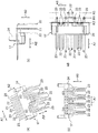
図4は、特許文献1に開示されたものとは異なるが形態が似ている従来の差動信号用コネクタに含まれるコンタクト組立体(以下「コンタクト・アッシー」ということもある)を示す。このコンタクト・アッシー1は、複数ペアの信号用コンタクト2と、複数のグランド用コンタクト3と、信号用コンタクト2及びグランド用コンタクト3を保持した絶縁性のハウジング4とを含んでいる。接続相手に接続するための第1の接続側では、信号用コンタクト2の各ペアの両側にグランド用コンタクト3を配置して一定ピッチのコンタクト列を形成している。さらに、信号用コンタクト2及びグランド用コンタクト3をコンタクト列と交差する方向に折り曲げ、基板に接続するための第2の接続側では、信号用コンタクト2及びグランド用コンタクト3を2列の千鳥状に配列にしている。
FIG. 4 shows a contact assembly (hereinafter also referred to as “contact assembly”) included in a conventional connector for differential signals which is different from that disclosed in Patent Document 1 but has a similar form. The contact assembly 1 includes a plurality of pairs of
図5は、図4のコンタクト・アッシー1を含む差動信号用コネクタを実装するための基板5を示す。この基板には複数のスルーホール6が形成されている。これらのスルーホール6は、差動信号用コネクタの第2の接続側における信号用コンタクト2及びグランド用コンタクト3の配列に対応して2列の千鳥状に配列されている。
FIG. 5 shows a
差動信号用コネクタ1を基板5に実装したとき、信号用コンタクト2及びグランド用コンタクト3はスルーホール6に挿入される。スルーホール6の開口の周囲には、ドーナツ状の導体パターンよりなるランド7がそれぞれ形成されている。そして、信号用コンタクト2を挿入されるスルーホール6に対応して形成されたランド7のみから、配線パターン8が基板5に沿って並列に引き出されている。したがって、信号用コンタクト2はスルーホール6及びランド7を介して配線パターン8に接続される。
When the differential signal connector 1 is mounted on the
上述した差動信号用コネクタにおいて、信号用コンタクト及びグランド用コンタクトを第2の接続側で2列の千鳥状に配列すること自体は、コネクタの小型化を容易に可能にする。しかし、実際にコネクタの小型化を図ると、ペアをなす差動信号用コンタクトの長さに差が生じることに起因する次の問題がある。 In the differential signal connector described above, the arrangement of the signal contacts and the ground contacts in two rows in a staggered manner on the second connection side itself enables the miniaturization of the connector easily. However, when the size of the connector is actually reduced, there is the following problem due to the difference in the length of the differential signal contacts forming a pair.
複数ペアの信号用コンタクト及び複数のグランド用コンタクトは、図6に示すように一枚の導体板に打ち抜き加工を施した後にさらに折り曲げ加工を施すことにより、纏めて製造することができる。その際の製造工程を容易にするために、コンタクト先端は等間隔、コンタクト折り曲げ回数は2回とするのが当業者の常識であった。しかし、コンタクト展開図の状態では、コンタクト先端間隔を等間隔にするために、ペアをなす差動信号用コンタクトの長さに差が生じている。この長さの差は、差動信号用コネクタにおいて差動信号対に伝播時間差(スキュー)を引き起こす原因になる。 A plurality of pairs of signal contacts and a plurality of ground contacts can be manufactured together by punching one conductor plate and then bending it as shown in FIG. In order to facilitate the manufacturing process at that time, it was common knowledge of those skilled in the art that the contact tips are equally spaced and the number of contact folding times is two. However, in the state of the contact development view, there is a difference in the lengths of the differential signal contacts that form a pair in order to make the contact tip intervals equal. This difference in length causes a difference in propagation time (skew) in the differential signal pair in the differential signal connector.
また、この長さの差に起因して、第2の接続側即ち基板上では、ペアをなす差動信号用コンタクト同士、その両脇のグランド用コンタクト同士、がそれぞれ同列ではなく2列に分かれて、配置されることがある。その場合、異なる列に形成されたランドから異なる長さをもって引き出された配線パターンがあることからも分かるように、ペアをなす信号用コンタクトに接続される対の配線パターンの長さに差が生じることがある。対の配線パターンの長さの差も、差動信号対にスキューを引き起こす原因になる。 Further, due to the difference in length, the differential signal contacts forming a pair and the ground contacts on both sides of the second connection side, that is, on the substrate, are divided into two rows instead of the same row. May be placed. In this case, as can be seen from the fact that there are wiring patterns drawn out with different lengths from lands formed in different rows, there is a difference in the lengths of the paired wiring patterns connected to the paired signal contacts. Sometimes. The difference in the length of the pair of wiring patterns also causes a skew in the differential signal pair.
それ故に本発明の課題は、小型でかつ差動信号対のスキューを小さくできる差動信号用コネクタを提供することにある。 Therefore, an object of the present invention is to provide a differential signal connector that is small in size and can reduce the skew of a differential signal pair.
本発明の一態様によれば、複数ペアの信号用コンタクトと、複数のグランド用コンタクトと、前記信号用コンタクト及び前記グランド用コンタクトを保持した絶縁性のハウジングとを含む差動信号用コネクタであって、接続相手に接続するための第1の接続側と、基板に接続するための第2の接続側とを有し、前記第1の接続側では、前記信号用コンタクトの各ペアの両側に前記グランド用コンタクトを配置して一定ピッチのコンタクト列を形成し、前記第2の接続側では、前記複数のグランド用コンタクトを第1の列に互いに離間して配置すると共に、前記第1の接続側で前記グランド用コンタクトの両側に配置された前記信号用コンタクトのペアを、前記第1の列の両側に位置する第2の列及び第3の列に振り分けて配置し、これにより前記第2の接続側では前記信号用コンタクトのペアを千鳥状配列としたことを特徴とする差動信号用コネクタが得られる。 According to one aspect of the present invention, there is provided a differential signal connector including a plurality of pairs of signal contacts, a plurality of ground contacts, and an insulating housing that holds the signal contacts and the ground contacts. A first connection side for connection to the connection partner and a second connection side for connection to the substrate, and on the first connection side, on both sides of each pair of the signal contacts The ground contacts are arranged to form contact rows with a constant pitch, and on the second connection side, the plurality of ground contacts are arranged apart from each other in the first row, and the first connection The signal contact pairs arranged on both sides of the ground contact on the side are distributed and arranged in the second and third rows located on both sides of the first row, thereby Serial in the second connecting side connector for differential signals, characterized in that the pair of contacts for the signal and staggered sequence is obtained.
本発明の一態様によるコネクタは、小型化が容易に可能でかつ差動信号対のスキューを小さくすることができる。 The connector according to one embodiment of the present invention can be easily downsized and the skew of the differential signal pair can be reduced.
図1を参照して、本発明の実施形態に係る差動信号用コネクタについて説明する。 A differential signal connector according to an embodiment of the present invention will be described with reference to FIG.
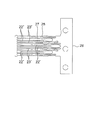
図1の差動信号用コネクタ10は上下2列のコンタクトを持つ20芯のプリント基板実装型コネクタであり、使用に際してはプリント基板11に実装される。差動信号用コネクタ10の接続相手となる相手コネクタ(図示せず)が接続される正面側を第1の接続側と呼び、プリント基板11に接続される底面側を第2の接続側と呼ぶ。第1の接続側には、相手コネクタが嵌合するための嵌合突起12が嵌合面と平行に左右に長くのびた形状をもって備えられている。第2の接続側については、後文にて詳述する。
The
ここで使用したプリント基板11は多層基板である。このプリント基板11には、下面11aを示す図1(c)から分かるように、多数のスルーホール13が形成されている。スルーホール13の開口の周囲には、ドーナツ状の導体パターンよりなるランド14がそれぞれ形成されている。またランド14の幾つかから配線パターン15が基板11に沿って並列に引き出されている。スルーホール13の位置及び役割については、後文にて明らかにする。
The printed
差動信号用コネクタ10は、上側コンタクト組立体(以下「上側コンタクト・アッシー」ということもある)16と、下側コンタクト組立体(以下「下側コンタクト・アッシー」ということもある)17と、上側及び下側コンタクト・アッシー16,17を纏めて囲った導電性のコネクタシェル18とを含んでいる。上側コンタクト・アッシー16は、ここでは付加コンタクトと呼ぶ多数の導電性の上側コンタクト19と、これらの上側コンタクト19を保持した絶縁性の上側ハウジング21とを備えている。上側コンタクト19は、その前端を嵌合突起12の上部に配列され、さらに後方にのびて下方に直角に曲がり、下端をプリント基板11の上面(図示せず)の配線パターンにSMT構造によりはんだ付けされる。コネクタシェル18は、プリント基板11に固定される複数の固定用脚部18a,18bを有している。これらの固定用脚部18a,18bがプリント基板11に係合することにより、差動信号用コネクタ10はプリント基板11にしっかりと固定される。下側コンタクト・アッシー17については、後文にて詳述する。
The
次に図1と共に図2をも参照して、下側コンタクト・アッシー17について詳述する。
Next, the
下側コンタクト・アッシー17は、3ペアの導電性の信号用コンタクト22と、4本の導電性のグランド用コンタクト23と、信号用コンタクト22及びグランド用コンタクト23を保持した絶縁性の下側ハウジング24とを含んでいる。下側ハウジング24の第1の接続側では、信号用コンタクト22の各ペアの両側にグランド用コンタクト23を配置した状態で第1の方向A1にのびた一定ピッチ(0.7mm以下が好ましい)のコンタクト列を形成している。
The
信号用コンタクト22及びグランド用コンタクト23は全て、第1の方向A1に直交する第2の方向A2で後方にのびて下側ハウジング24を貫通した後に、下側ハウジング24の反対側で直角に折り曲げられ、第1の方向A1及び第2の方向A2に直交する第3の方向A3で下方にのびている。以下の説明では、信号用コンタクト22及びグランド用コンタクト23を纏めて下側コンタクト25と呼ぶこともある。
All of the
図1から分かるように、差動信号用コネクタ10の第1の接続側では、下側コンタクト25は嵌合突起12の下部に上側コンタクト19と間隔をおいて対向するように配列されている。したがって、相手コネクタは嵌合突起12に嵌合したときに上側コンタクト19及び下側コンタクト25に接触し、その結果、差動信号用コネクタ10に電気的に接続される。ここで、下側コンタクト25のうち、相手コネクタに接触する部分をコネクタ接触部と呼ぶ。
As can be seen from FIG. 1, on the first connection side of the
一方、差動信号用コネクタ10の第2の接続側では、下側コンタクト25はプリント基板11のスルーホール13に挿入され、プリント基板11の下面11aにおいてランド14に半田付けにより接続される。プリント基板11の下面11aにおいて半田付けされるため、コネクタ実装時に目視により半田付けの良否を容易に判定できる。ここで、下側コンタクト25のうち、スルーホール13に挿入される部分を基板接続部と呼ぶ。
On the other hand, on the second connection side of the
プリント基板11のスルーホール13の穴径は、コンタクトが断面四角形の場合には少なくともコンタクトの対角長よりわずかに大きく設計される。さらに、スルーホール13の周囲にはランド14が形成され、また隣接するスルーホール13と絶縁をとることも必要である。これらを考慮し、スルーホール13には0.8mm程度の間隔を設定することが好ましい。
The diameter of the through
図2において、下側コンタクト25の基板接続部は、第2の方向A2で互いに離間して第1の方向A1にのびた平行な3列に分けて配置されている。具体的に述べると、複数のグランド用コンタクト23の基板接続部を第1の列R1に互いに離間して配置すると共に、コネクタ接触部がグランド用コンタクト23の両側に配置されている信号用コンタクト22のペアを、第1の列R1の両側に位置する第2の列R2及び第3の列R3に振り分けて配置している。この結果、信号用コンタクト22のペアの基板接続部は図3からよく分かるように第1の列R1の両側に千鳥状配列とされている。
In FIG. 2, the substrate connecting portions of the
ここで、複数の信号用コンタクト22のうち、第2の列R2に配置されたものを実質的に同じ長さに設計し、かつ、第3の列R3に配置されたものを実質的に同じ長さに設計している。即ち、同列に配置された信号用コンタクト22のペアの長さを等長にしている。そして、信号用コンタクト22の第1の接続部側と第2の接続部側との間での折り曲げの違い、具体的には、折り曲げ位置の違いにより、信号用コンタクト22のペアを第2の列及び前記第3の列R3に振り分けている。またグランド用コンタクト23は、第1の接続部側と第2の接続部側との間での信号用コンタクト22との折り曲げ位置の違いにより、第1の列R1に配置している。なお、折り曲げ位置に違いをもたせる代わりに、信号用コンタクト22及びグランド用コンタクト23を折り曲げ回数の違いによって第2の接続部側で3列に配列させることも可能であるし、また両者を併用してもよい。
Here, among the plurality of
さらに、第2の接続側では、信号用コンタクト22の各ペアをグランド用コンタクト23の隣接したものの間に対応させて配置し、しかも信号用コンタクト22の各ペア内のピッチをコンタクト列のピッチよりも少し大きく設計している。
Further, on the second connection side, each pair of
また、グランド用コンタクト23を信号用コンタクト22のペアとペアとの間に対応させて配置すると共に、第1の接続側においてはグランド用コンタクト23とこれの両側に隣接配置されている二つの信号用コンタクト22とを、第2の接続側においては第1、第2、及び第3の列R1,R2,R3に対し斜めに交差する方向に配列している。
In addition, the
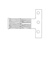
上述した3ペアの導電性の信号用コンタクト22と4本の導電性のグランド用コンタクト23は、図3に示す展開図のように、1枚の導体板26からプレス加工により形成することが容易に可能である。導体板26において、信号用コンタクト22及びグランド用コンタクト23となる部分には参照符号22′及び23′をそれぞれ付し、また折り曲げる部分には参照符号27及び28をそれぞれ付している。
The three pairs of
なお、プリント基板11の多数のスルーホール13は、第2の接続側における信号用コンタクト22及びグランド用コンタクト23の上述したような配置に対応した位置に形成されることは勿論である。
Needless to say, the numerous through
以下に、さらに具体的に説明する。 More specific description will be given below.
多数の下側コンタクト25は図3の上側から、グランド用コンタクト23’,信号用コンタクト22’,信号用コンタクト22’、グランド用コンタクト23’、信号用コンタクト22’、信号用コンタクト22’、グランド用コンタクト23’、信号用コンタクト22’、信号用コンタクト22’、及びグランド用コンタクト23’の順に配列されている。
A large number of
ここで、互いに隣接したペアの信号用コンタクト22は逆位相の信号からなる差動信号対を伝送するラインを接続するものであるため、以下の説明ではそれぞれ+Sigコンタクト、−Sigコンタクトと呼ぶ。また、スルーホール13のうち、+Sigコンタクトが挿入されるものを+Sigスルーホールと呼び、−Sigコンタクトが挿入されるものを−Sigスルーホールと呼び、グランド用コンタクト23が挿入されるものをGNDスルーホールと呼ぶ。また、配線パターン15のうち、+Sigスルーホールに接続されたものを+Sig配線パターンと呼び、−Sigスルーホールに接続されたものを−Sig配線パターンと呼ぶ。
Here, the pair of
上述した差動信号用コネクタによると、+Sigスルーホールと−Sigスルーホールがコネクタ嵌合面と平行に配置されるので、多層基板であるプリント基板11の下面11aにおいて+Sig配線パターンと−Sig配線パターンとを、コネクタ後方に平行でかつ等長な配線パターンとすることが可能となる。したがって、差動信号内のスキューが少なく、なお、上述では一対の差動信号を伝送するラインを接続する場合について説明したが、複数対の差動信号を伝送する場合においても同様でありかつ同様の効果を得ることができる。
According to the differential signal connector described above, since the + Sig through hole and the −Sig through hole are arranged in parallel with the connector fitting surface, the + Sig wiring pattern and the −Sig wiring pattern on the
なお、本発明は上記実施形態に限られることはなく、またその一部又は全部は以下の付記のようにも記載され得るがそれらには限られない。 In addition, this invention is not limited to the said embodiment, The one part or all part can also be described like the following additional remarks, but it is not restricted to them.
(付記1)
複数ペアの信号用コンタクトと、複数のグランド用コンタクトと、前記信号用コンタクト及び前記グランド用コンタクトを保持した絶縁性のハウジングとを含む差動信号用コネクタであって、
接続相手に接続するための第1の接続側と、基板に接続するための第2の接続側とを有し、
前記第1の接続側では、前記信号用コンタクトの各ペアの両側に前記グランド用コンタクトを配置して一定ピッチのコンタクト列を形成し、
前記第2の接続側では、前記複数のグランド用コンタクトを第1の列に互いに離間して配置すると共に、前記第1の接続側で前記グランド用コンタクトの両側に配置された前記信号用コンタクトのペアを、前記第1の列の両側に位置する第2の列及び第3の列に振り分けて配置し、これにより前記第2の接続側では前記信号用コンタクトのペアを千鳥状配列とした
ことを特徴とする差動信号用コネクタ。
(Appendix 1)
A differential signal connector including a plurality of pairs of signal contacts, a plurality of ground contacts, and an insulating housing holding the signal contacts and the ground contacts,
Having a first connection side for connecting to the connection partner and a second connection side for connecting to the substrate;
On the first connection side, the ground contacts are arranged on both sides of each pair of the signal contacts to form a contact row having a constant pitch,
On the second connection side, the plurality of ground contacts are arranged apart from each other in a first row, and the signal contacts arranged on both sides of the ground contact on the first connection side are arranged. The pairs are distributed and arranged in the second and third rows located on both sides of the first row, whereby the signal contact pairs are arranged in a staggered arrangement on the second connection side. A connector for differential signals.
(付記2)
前記複数の信号用コンタクトのうち、前記第2の列に配置されたものを実質的に同じ長さに設計し、かつ、前記第3の列に配置されたものを実質的に同じ長さに設計した、付記1に記載の差動信号用コネクタ。
(Appendix 2)
Among the plurality of signal contacts, those arranged in the second row are designed to have substantially the same length, and those arranged in the third row have substantially the same length. The differential signal connector according to Supplementary Note 1, which is designed.
(付記3)
前記信号用コンタクトを前記第1の接続部側と前記第2の接続部側との間で前記コンタクト列と交差する方向に折り曲げ、その折り曲げの違いにより、前記信号用コンタクトのペアを前記第2の列及び前記第3の列に振り分けた、付記1又は2に記載の差動信号用コネクタ。
(Appendix 3)
The signal contact is bent in a direction intersecting the contact row between the first connection portion side and the second connection portion side, and the pair of signal contacts is changed to the second connection portion by the difference in bending. The differential signal connector according to
(付記4)
前記グランド用コンタクトを前記第1の接続部側と前記第2の接続部側との間で前記コンタクト列と交差する方向に折り曲げ、前記グランド用コンタクトを第1の列に配置した、付記3に記載の差動信号用コネクタ。
(Appendix 4)
(付記5)
前記第2の接続側では、前記信号用コンタクトの各ペアを前記グランド用コンタクトの隣接したものの間に対応させて配置した、付記1−4のいずれか一項に記載の差動信号用コネクタ。
(Appendix 5)
5. The differential signal connector according to claim 1, wherein, on the second connection side, each pair of the signal contacts is disposed so as to correspond between adjacent ones of the ground contacts.
(付記6)
前記第2の接続側では、前記信号用コンタクトのペア内のピッチを前記コンタクト列のピッチよりも大きく設計した、付記1−5のいずれか一項に記載の差動信号用コネクタ。
(Appendix 6)
The differential signal connector according to any one of appendices 1-5, wherein, on the second connection side, a pitch in the pair of signal contacts is designed to be larger than a pitch of the contact row.
(付記7)
前記第2の接続側では、前記グランド用コンタクトを前記信号用コンタクトのペアとペアとの間に対応させて配置した、付記1−6のいずれか一項に記載の差動信号用コネクタ。
(Appendix 7)
The differential signal connector according to any one of appendices 1-6, wherein, on the second connection side, the ground contact is disposed so as to correspond to the pair of signal contacts.
(付記8)
前記第2の接続側では、前記第1の接続側においては前記グランド用コンタクトとこれの両側に隣接配置されている二つの信号用コンタクトとを、前記第1の列に対し斜めに交差する方向に配列させた、付記1−7のいずれか一項に記載の差動信号用コネクタ。
(Appendix 8)
In the second connection side, in the first connection side, the ground contact and two signal contacts arranged adjacent to both sides thereof are obliquely intersected with the first row. The connector for differential signals according to any one of appendices 1-7, arranged in an array.
(付記9)
前記第1の列、前記第2の列、及び前記第3の列が互いに平行である、付記1−8のいずれか一項に記載の差動信号用コネクタ。
(Appendix 9)
The differential signal connector according to any one of appendices 1-8, wherein the first row, the second row, and the third row are parallel to each other.
(付記10)
さらに、複数の付加コンタクトを含み、前記第1の接続側では、前記付加コンタクトを前記コンタクト列に間隔をおいて対向するように配列させた、付記1−9のいずれか一項に記載の差動信号用コネクタ。
(Appendix 10)
The difference according to any one of appendices 1-9, further including a plurality of additional contacts, wherein, on the first connection side, the additional contacts are arranged to be opposed to the contact row with a space therebetween. Motion signal connector.
1 コンタクト組立体(コンタクト・アッシー)
2 信号用コンタクト
3 グランド用コンタクト
4 ハウジング
5 基板
6 スルーホール
7 ランド
8 配線パターン
10 差動信号用コネクタ
11 プリント基板
11a (プリント基板)下面
12 嵌合突起
13 スルーホール
14 ランド
15 配線パターン
16 上側コンタクト組立体(上側コンタクト・アッシー)
17 下側コンタクト組立体(下側コンタクト・アッシー)
18 コネクタシェル
18a,18b 固定用脚部
19 上側コンタクト
21 上側ハウジング
22 信号用コンタクト
22’ 導体板の信号用コンタクトとなる部分
23 グランド用コンタクト
23’ 導体板のグランド用コンタクトとなる部分
24 下側ハウジング(請求項記載のハウジング)
25 下側コンタクト
26 導体板
27,28 折り曲げる部分
R1 第1の列
R2 第2の列
R3 第3の列
1 Contact assembly (contact assembly)
DESCRIPTION OF
17 Lower contact assembly (lower contact assembly)
18
25
本発明の一態様によれば、複数ペアの信号用コンタクトと、複数のグランド用コンタクトと、前記信号用コンタクト及び前記グランド用コンタクトを保持した絶縁性のハウジングとを含む差動信号用コネクタであって、接続相手に接続するための第1の接続側と、基板に接続するための第2の接続側とを有し、前記第1の接続側では、前記信号用コンタクトの各ペアの両側に前記グランド用コンタクトを配置して一定ピッチのコンタクト列を形成し、前記第2の接続側では、前記複数のグランド用コンタクトを第1の列に互いに離間して配置すると共に、前記第1の接続側で前記グランド用コンタクトの両側に隣接配置された前記信号用コンタクトの2つのペアを、前記第1の列の両側に位置する第2の列及び第3の列に振り分けて配置し、これにより前記第2の接続側では前記信号用コンタクトの複数ペアを千鳥状配列としたことを特徴とする差動信号用コネクタが得られる。
本発明の他の態様によれば、複数のコンタクトと前記コンタクトを保持した絶縁性のハウジングとを含むコネクタであって、接続相手に接続するための第1の接続側と、基板に接続するための第2の接続側とを有し、前記コンタクトを、前記第2の接続側における中央の第1の列に互いに間隔をもって配置された複数の第1のコンタクトと、前記第1の列の両側に位置する第2の列及び第3の列に振り分けて複数ペアとして配置された複数の第2のコンタクトとに分け、前記第2の接続側では、前記第2のコンタクトの複数ペアを、前記第2の列に配置されたものと前記第3の列に配置されたものとが前記第1のコンタクトの隣接した間隔に交互に対向するように配置し、これにより前記第2の接続側では前記第1の列の両側に前記第2のコンタクトの複数ペアを千鳥状配列とし、前記第1の接続側では、前記第1のコンタクトを互いに間隔をもって一列に配置すると共に、前記第2のコンタクトの複数ペアを、前記第1のコンタクトの隣接した間隔内に一列に配置し、これにより前記第1の接続側では前記第1のコンタクト及び前記第2のコンタクトが一列のコンタクト列を形成したことを特徴とするコネクタが得られる。
According to one aspect of the present invention, there is provided a differential signal connector including a plurality of pairs of signal contacts, a plurality of ground contacts, and an insulating housing that holds the signal contacts and the ground contacts. A first connection side for connection to the connection partner and a second connection side for connection to the substrate, and on the first connection side, on both sides of each pair of the signal contacts The ground contacts are arranged to form contact rows with a constant pitch, and on the second connection side, the plurality of ground contacts are arranged apart from each other in the first row, and the first connection two pairs of the signal contacts disposed adjacent to opposite sides of the ground contact on the side, by distributing the second row and the third row positioned on either side of the first row are arranged, In said second connection side differential signal connector, characterized in that a plurality pairs of contacts for the signals and with staggered obtained by Les.
According to another aspect of the present invention, there is provided a connector including a plurality of contacts and an insulative housing that holds the contacts, the first connection side for connecting to a connection partner, and the connection to the substrate. A plurality of first contacts spaced from each other in a central first row on the second connection side, and both sides of the first row. And divided into a plurality of second contacts arranged as a plurality of pairs divided into a second row and a third row located on the second connection side, and on the second connection side, the plurality of pairs of the second contacts are Those arranged in the second row and those arranged in the third row are arranged so as to be alternately opposed to the adjacent intervals of the first contact, whereby the second connection side The second links on either side of the first row. A plurality of pairs of tacts are arranged in a staggered arrangement, and on the first connection side, the first contacts are arranged in a line at intervals, and a plurality of pairs of the second contacts are adjacent to the first contacts. Thus, a connector is obtained in which the first contacts and the second contacts form one contact row on the first connection side.
Claims (10)
接続相手に接続するための第1の接続側と、基板に接続するための第2の接続側とを有し、
前記第1の接続側では、前記信号用コンタクトの各ペアの両側に前記グランド用コンタクトを配置して一定ピッチのコンタクト列を形成し、
前記第2の接続側では、前記複数のグランド用コンタクトを第1の列に互いに離間して配置すると共に、前記第1の接続側で前記グランド用コンタクトの両側に配置された前記信号用コンタクトのペアを、前記第1の列の両側に位置する第2の列及び第3の列に振り分けて配置し、これにより前記第2の接続側では前記信号用コンタクトのペアを千鳥状配列とした
ことを特徴とする差動信号用コネクタ。 A differential signal connector including a plurality of pairs of signal contacts, a plurality of ground contacts, and an insulating housing holding the signal contacts and the ground contacts,
Having a first connection side for connecting to the connection partner and a second connection side for connecting to the substrate;
On the first connection side, the ground contacts are arranged on both sides of each pair of the signal contacts to form a contact row having a constant pitch,
On the second connection side, the plurality of ground contacts are arranged apart from each other in a first row, and the signal contacts arranged on both sides of the ground contact on the first connection side are arranged. The pairs are distributed and arranged in the second and third rows located on both sides of the first row, whereby the signal contact pairs are arranged in a staggered arrangement on the second connection side. A connector for differential signals.
Priority Applications (18)
| Application Number | Priority Date | Filing Date | Title |
|---|---|---|---|
| JP2011037321A JP5826500B2 (en) | 2011-02-23 | 2011-02-23 | connector |
| US13/357,157 US8951050B2 (en) | 2011-02-23 | 2012-01-24 | Differential signal connector capable of reducing skew between a differential signal pair |
| CA2866429A CA2866429C (en) | 2011-02-23 | 2012-02-09 | Differential signal connector capable of reducing skew between a differential signal pair |
| CA2866423A CA2866423C (en) | 2011-02-23 | 2012-02-09 | Differential signal connector capable of reducing skew between a differential signal pair |
| CA2767669A CA2767669C (en) | 2011-02-23 | 2012-02-09 | Differential signal connector capable of reducing skew between a differential signal pair |
| CA2866434A CA2866434C (en) | 2011-02-23 | 2012-02-09 | Differential signal connector capable of reducing skew between a differential signal pair |
| CA2866439A CA2866439C (en) | 2011-02-23 | 2012-02-09 | Differential signal connector capable of reducing skew between a differential signal pair |
| KR20120014200A KR101495399B1 (en) | 2011-02-23 | 2012-02-13 | Differential signal connector capable of reducing skew between a differential signal pair |
| CN2012100367986A CN102683941A (en) | 2011-02-23 | 2012-02-17 | Differential signal connector capable of reducing skew between a differential signal pair |
| CN2012206824482U CN203103565U (en) | 2011-02-23 | 2012-02-17 | Differential signal connector and lead frame |
| CN2012200537484U CN202888439U (en) | 2011-02-23 | 2012-02-17 | Differential signal connector and lead frame |
| CN201410225106.1A CN104022381A (en) | 2011-02-23 | 2012-02-17 | Differential signal connector capable of reducing skew between differential signal pair |
| TW101105559A TWI544696B (en) | 2011-02-23 | 2012-02-21 | Differential signal connector capable of reducing skew between a differential signal pair |
| DE102012202706A DE102012202706A1 (en) | 2011-02-23 | 2012-02-22 | Differential signal connector, which can reduce an offset between a differential signal pair |
| US14/021,123 US8894451B2 (en) | 2011-02-23 | 2013-09-09 | Differential signal connector capable of reducing skew between a differential signal pair |
| KR1020140094798A KR101534446B1 (en) | 2011-02-23 | 2014-07-25 | Differential signal connector capable of reducing skew between a differential signal pair |
| US14/474,949 US9490589B2 (en) | 2011-02-23 | 2014-09-02 | Differential signal connector capable of reducing skew between a differential signal pair |
| US14/518,048 US9450343B2 (en) | 2011-02-23 | 2014-10-20 | Differential signal connector capable of reducing skew between a differential signal pair |
Applications Claiming Priority (1)
| Application Number | Priority Date | Filing Date | Title |
|---|---|---|---|
| JP2011037321A JP5826500B2 (en) | 2011-02-23 | 2011-02-23 | connector |
Related Child Applications (1)
| Application Number | Title | Priority Date | Filing Date |
|---|---|---|---|
| JP2012087700A Division JP5683521B2 (en) | 2012-04-06 | 2012-04-06 | Conductor plate and differential signal connector |
Publications (3)
| Publication Number | Publication Date |
|---|---|
| JP2012174597A true JP2012174597A (en) | 2012-09-10 |
| JP2012174597A5 JP2012174597A5 (en) | 2012-10-18 |
| JP5826500B2 JP5826500B2 (en) | 2015-12-02 |
Family
ID=46977321
Family Applications (1)
| Application Number | Title | Priority Date | Filing Date |
|---|---|---|---|
| JP2011037321A Expired - Fee Related JP5826500B2 (en) | 2011-02-23 | 2011-02-23 | connector |
Country Status (1)
| Country | Link |
|---|---|
| JP (1) | JP5826500B2 (en) |
Cited By (3)
| Publication number | Priority date | Publication date | Assignee | Title |
|---|---|---|---|---|
| WO2016140659A1 (en) * | 2015-03-04 | 2016-09-09 | Hewlett Packard Enterprise Development Lp | Multiple pins of different lengths corresponding to different data signaling rates |
| JP2020030978A (en) * | 2018-08-23 | 2020-02-27 | 株式会社デンソー | Substrate module |
| JP7492449B2 (en) | 2020-12-17 | 2024-05-29 | ケル株式会社 | connector |
Families Citing this family (2)
| Publication number | Priority date | Publication date | Assignee | Title |
|---|---|---|---|---|
| JP7387412B2 (en) | 2019-12-03 | 2023-11-28 | 日本航空電子工業株式会社 | connector assembly |
| JP7446094B2 (en) | 2019-12-03 | 2024-03-08 | 日本航空電子工業株式会社 | Connection objects, connectors, and harnesses |
Citations (1)
| Publication number | Priority date | Publication date | Assignee | Title |
|---|---|---|---|---|
| JP2008041656A (en) * | 2006-07-14 | 2008-02-21 | Japan Aviation Electronics Industry Ltd | Connector |
-
2011
- 2011-02-23 JP JP2011037321A patent/JP5826500B2/en not_active Expired - Fee Related
Patent Citations (1)
| Publication number | Priority date | Publication date | Assignee | Title |
|---|---|---|---|---|
| JP2008041656A (en) * | 2006-07-14 | 2008-02-21 | Japan Aviation Electronics Industry Ltd | Connector |
Cited By (5)
| Publication number | Priority date | Publication date | Assignee | Title |
|---|---|---|---|---|
| WO2016140659A1 (en) * | 2015-03-04 | 2016-09-09 | Hewlett Packard Enterprise Development Lp | Multiple pins of different lengths corresponding to different data signaling rates |
| US10063011B2 (en) | 2015-03-04 | 2018-08-28 | Hewlett Packard Enterprise Development Lp | Multiple pins of different lengths corresponding to different data signaling rates |
| JP2020030978A (en) * | 2018-08-23 | 2020-02-27 | 株式会社デンソー | Substrate module |
| CN110859023A (en) * | 2018-08-23 | 2020-03-03 | 株式会社电装 | Circuit board module and method for assembling circuit board module |
| JP7492449B2 (en) | 2020-12-17 | 2024-05-29 | ケル株式会社 | connector |
Also Published As
| Publication number | Publication date |
|---|---|
| JP5826500B2 (en) | 2015-12-02 |
Similar Documents
| Publication | Publication Date | Title |
|---|---|---|
| JP6648185B2 (en) | Impedance control electrical connector | |
| JP5986012B2 (en) | Connector and signal transmission method using the same | |
| US6935870B2 (en) | Connector having signal contacts and ground contacts in a specific arrangement | |
| KR101123524B1 (en) | Electrical connector | |
| JP4862796B2 (en) | High-density connector for high-speed transmission | |
| JP3179306U (en) | Mini display port connector | |
| JP4613043B2 (en) | connector | |
| TWI670899B (en) | Connector | |
| JP4542579B2 (en) | connector | |
| US20140370728A1 (en) | Differential signal connector capable of reducing skew between a differential signal pair | |
| JP3150703U (en) | Electrical connector suitable for high-frequency signal transmission | |
| JP2010245041A (en) | Electrical connector | |
| JP2007115707A (en) | Receptacle | |
| JP5826500B2 (en) | connector | |
| TWI496359B (en) | Lead frame, method of manufacturing a contact group, and connector | |
| KR20120112497A (en) | Board mounted connector | |
| JP2007200575A (en) | Multi-pole connector and portable wireless terminal or small-sized electronic apparatus using same | |
| JP2007214139A (en) | Mounting structure for receptacle | |
| TWI373891B (en) | Connector | |
| JP5683521B2 (en) | Conductor plate and differential signal connector | |
| JP5813449B2 (en) | Lead frame and connector | |
| JP2013084472A (en) | Contact group and connector | |
| KR100827267B1 (en) | Electrical connector capable of suppressing crosstalk | |
| JP2009123405A (en) | Edge connector | |
| JP2006114407A (en) | Connector device |
Legal Events
| Date | Code | Title | Description |
|---|---|---|---|
| A521 | Request for written amendment filed |
Free format text: JAPANESE INTERMEDIATE CODE: A523 Effective date: 20120727 |
|
| A621 | Written request for application examination |
Free format text: JAPANESE INTERMEDIATE CODE: A621 Effective date: 20140217 |
|
| A131 | Notification of reasons for refusal |
Free format text: JAPANESE INTERMEDIATE CODE: A131 Effective date: 20141210 |
|
| A521 | Request for written amendment filed |
Free format text: JAPANESE INTERMEDIATE CODE: A523 Effective date: 20150127 |
|
| A02 | Decision of refusal |
Free format text: JAPANESE INTERMEDIATE CODE: A02 Effective date: 20150507 |
|
| A521 | Request for written amendment filed |
Free format text: JAPANESE INTERMEDIATE CODE: A523 Effective date: 20150716 |
|
| A911 | Transfer to examiner for re-examination before appeal (zenchi) |
Free format text: JAPANESE INTERMEDIATE CODE: A911 Effective date: 20150727 |
|
| A131 | Notification of reasons for refusal |
Free format text: JAPANESE INTERMEDIATE CODE: A131 Effective date: 20150819 |
|
| A521 | Request for written amendment filed |
Free format text: JAPANESE INTERMEDIATE CODE: A523 Effective date: 20150901 |
|
| A521 | Request for written amendment filed |
Free format text: JAPANESE INTERMEDIATE CODE: A523 Effective date: 20150910 |
|
| TRDD | Decision of grant or rejection written | ||
| A01 | Written decision to grant a patent or to grant a registration (utility model) |
Free format text: JAPANESE INTERMEDIATE CODE: A01 Effective date: 20150930 |
|
| A61 | First payment of annual fees (during grant procedure) |
Free format text: JAPANESE INTERMEDIATE CODE: A61 Effective date: 20151014 |
|
| R150 | Certificate of patent or registration of utility model |
Ref document number: 5826500 Country of ref document: JP Free format text: JAPANESE INTERMEDIATE CODE: R150 |
|
| RD04 | Notification of resignation of power of attorney |
Free format text: JAPANESE INTERMEDIATE CODE: R3D04 |
|
| R250 | Receipt of annual fees |
Free format text: JAPANESE INTERMEDIATE CODE: R250 |
|
| R250 | Receipt of annual fees |
Free format text: JAPANESE INTERMEDIATE CODE: R250 |
|
| R250 | Receipt of annual fees |
Free format text: JAPANESE INTERMEDIATE CODE: R250 |
|
| R250 | Receipt of annual fees |
Free format text: JAPANESE INTERMEDIATE CODE: R250 |
|
| LAPS | Cancellation because of no payment of annual fees |