JP2012169548A - Pickup method of chip-shaped component - Google Patents
Pickup method of chip-shaped component Download PDFInfo
- Publication number
- JP2012169548A JP2012169548A JP2011031136A JP2011031136A JP2012169548A JP 2012169548 A JP2012169548 A JP 2012169548A JP 2011031136 A JP2011031136 A JP 2011031136A JP 2011031136 A JP2011031136 A JP 2011031136A JP 2012169548 A JP2012169548 A JP 2012169548A
- Authority
- JP
- Japan
- Prior art keywords
- chip
- suction
- dicing tape
- heating
- dicing
- Prior art date
- Legal status (The legal status is an assumption and is not a legal conclusion. Google has not performed a legal analysis and makes no representation as to the accuracy of the status listed.)
- Withdrawn
Links
Images


Abstract
Description
本発明は、半導体チップなどのチップ状部品のピックアップ方法に関する。より詳細には、例えば、半導体チップ等の小型電子部品の製造工程において、加熱により変形する層を有するダイシングテープ上の保持されたチップ状部品を、ダイシングテープを加熱変形させることで接着力を低減し、チップ状部品をピックアップする方法に関する。 The present invention relates to a method for picking up a chip-shaped component such as a semiconductor chip. More specifically, for example, in the manufacturing process of small electronic parts such as semiconductor chips, the adhesive force is reduced by heat-deforming the dicing tape of the chip-like parts held on the dicing tape having a layer that is deformed by heating. And a method for picking up chip-shaped components.
従来より、半導体ウエハなどの多数の部品が形成された板状部品を部品毎のチップ体に分割する際には、ダイシングテープにより板状部材を固定して、部品毎に切断分離(ダイシング)するダイシング工程を行なっている。そして、このダイシング工程によって分割された個々のチップ状部品を、ダイシングテープからピックアップして(取り上げて)、例えば、別途用意したTABテープなどの電子部品実装用フィルムキャリアテープなどにダイボンディングして、半導体装置などの所望の装置を得ている。 Conventionally, when a plate-like component on which a large number of components such as a semiconductor wafer are formed is divided into chip bodies for each component, the plate-like member is fixed with a dicing tape and cut and separated (diced) for each component. A dicing process is performed. Then, the individual chip-like parts divided by this dicing process are picked up (taken up) from the dicing tape, for example, die-bonded to a film carrier tape for mounting electronic parts such as a separately prepared TAB tape, A desired device such as a semiconductor device is obtained.
チップ状部品をダイシングテープからピックアップする際には、ダイシングテープの背面から突き上げ針を突き上げて、チップ状物品をダイシングテープから剥離して、チップ状部品の上面より吸引コレットで吸引把持する方法が採用されている。近年、半導体ウエハは、実装効率を向上させるため、その厚さを極めて薄くするようになっている。このため、突き上げ時の衝撃で、チップ状部品が破損するおそれが高くなってきている。 When picking up chip-shaped parts from the dicing tape, a method is adopted in which the needle is pushed up from the back of the dicing tape, the chip-shaped article is peeled from the dicing tape, and sucked and held by the suction collet from the upper surface of the chip-shaped part. Has been. In recent years, semiconductor wafers have been made extremely thin in order to improve mounting efficiency. For this reason, there is an increased risk of damage to the chip-like component due to the impact at the time of pushing up.
特に近年では、チップの薄化傾向とともに貫通電極の設けられた、いわゆるTSV(Through Silicon Via)チップが用いられることが増えてきたが、このようなTSVチップ用のウエハには貫通電極が設けられており、隣接する貫通電極の間がわずかな衝撃でも破壊されやすいので、突き上げ針による突き上げを行わないピックアップ方法が求められている。 Particularly in recent years, so-called TSV (Through Silicon Via) chips provided with through electrodes have been used with the trend of thinning of the chips, but such TSV chip wafers are provided with through electrodes. Therefore, there is a need for a pickup method that does not push up with a push-up needle because the adjacent through-electrodes are easily broken even by a slight impact.
このような状況に鑑みて、本出願人は、特許文献1(特開平10−233373号公報)、特許文献2(特開平10−284446号公報)、特許文献3(特開平11−3875号公報)、特許文献4(特開2004−119992号公報)に開示されるように、ピックアップの際に、突き上げ針による突き上げを行なうことなく、吸引コレットによる吸引のみで、チップ状部品をダイシングテープからピックアップできるダイシングテープおよび装置を提案した。 In view of such circumstances, the present applicant has disclosed Patent Document 1 (Japanese Patent Laid-Open No. 10-233373), Patent Document 2 (Japanese Patent Laid-Open No. 10-284446), and Patent Document 3 (Japanese Patent Laid-Open No. 11-3875). ), And as disclosed in Japanese Patent Application Laid-Open No. 2004-199992, when picking up, a chip-like component is picked up from a dicing tape only by suction by a suction collet without being pushed up by a push-up needle. We proposed a dicing tape and equipment that can be used.
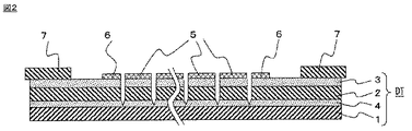
これら特許文献1〜4に開示されたダイシングテープを用いたピックアップ方法の概略的な機構を示せば、以下のとおりである。すなわち、図1に示すように、ダイシングテープDTは、非収縮性フィルム1と、収縮性フィルム2と、粘着剤層3とからなり、非収縮性フィルム1と、収縮性フィルム2とは直接積層されていてもよく、図示したように接着剤層4を介して積層されていてもよい。
The schematic mechanism of the pickup method using the dicing tape disclosed in
上記のようなダイシングテープDTの粘着剤層3を、半導体ウエハSWに貼着し、複数のチップにダイシングする。ダイシングの結果、半導体ウエハの周縁部も切断され、製品となるチップ状部品5のほか、後述する「周辺チップ6」も生成する。ダイシング時には、図2に示すように、半導体ウエハとともに収縮性フィルム2を完全に切断しておく。また、ダイシングテープDTの外周部はリングフレーム7により固定しておく。ダイシング直後には、各チップは、ダイシングブレードの幅の間隔で整列している。続いて、加熱により収縮性フィルム2を収縮させる。チップ直下の収縮性フィルム2の収縮に伴い、粘着剤層3も変形し、図3に示すように、チップ状部品5と粘着剤層3との接触面積が激減し、またこの際にチップ状部品5と粘着剤層3との間にずれ応力が生じるため、チップ状部品5と粘着剤層3との接着力が低下し、ピックアップが容易となる。
The adhesive layer 3 of the dicing tape DT as described above is attached to the semiconductor wafer SW and diced into a plurality of chips. As a result of the dicing, the peripheral portion of the semiconductor wafer is also cut, and the “
また、特許文献5(特開2002−280330号公報)には、上記のようなダイシングテープを用いて板状部材をダイシングし、ダイシングテープを加熱変形して、チップとダイシングテープとの間の接着力を低下した後に、ダイシングテープの背面側から吸引することで、さらにチップとダイシングテープとの間の接着力が低下し、ピックアップを容易にする技術が開示されている。 Further, in Patent Document 5 (Japanese Patent Laid-Open No. 2002-280330), a plate-like member is diced using the dicing tape as described above, the dicing tape is heated and deformed, and adhesion between the chip and the dicing tape is performed. A technique for facilitating pick-up is disclosed by further reducing the adhesive force between the chip and the dicing tape by sucking from the back side of the dicing tape after the force is reduced.
半導体チップに代表されるように、チップ状部品には、小型化、薄化、軽量化が求められ続けている。チップ状部品の小型化、薄化、軽量化が進められた結果、上記のようなダイシングテープを用いた際に、特に加熱工程において、いわゆる「周辺チップ」が飛散するなどの現象が多発するようになった。 As represented by semiconductor chips, chip-like components are continuously required to be reduced in size, thickness, and weight. As a result of the progress of miniaturization, thinning, and weight reduction of chip-shaped parts, when using the dicing tape as described above, phenomena such as so-called “peripheral chips” are likely to occur, especially in the heating process. Became.
図4に示すように、半導体ウエハSWを、回路8毎に区画するダイシングラインDLに沿って切断分離すると、内周部においては製品となるチップ状部品5が生成し、外周部にいわゆる「周辺チップ6」が生成する(以下、チップ状部品と周辺チップを総称して単に「チップ」と記載することがある)。周辺チップ6には通常回路が形成されておらず、また形状もいびつであり、製品とはならない。周辺チップの多くは三辺または二辺のみが切断された状態にある。
As shown in FIG. 4, when the semiconductor wafer SW is cut and separated along a dicing line DL that is divided for each
製品となるチップ状部品5に隣接する周辺チップ6の側部では、収縮性フィルム2が完全に切断されているが、リングフレーム7側の収縮性フィルム2は切断されていない。すなわち、チップ状部品5がリングフレームとは断絶した収縮性フィルム2上に粘着剤層3を介して保持されているのに対し、周辺チップ6は、一端がリングフレームに固定された収縮性フィルム2上に粘着剤層3を介して保持されている。
The
このような状態で収縮性フィルムの変形(収縮)を行うと、周辺チップ6が粘着剤層3から剥離し、飛散してしまうことがある。特に、チップの近年の小型化、薄化、軽量化により、周辺チップも同様に小型化、薄化、軽量化したため、このような飛散が起こりやすくなってきた。飛散した周辺チップ6は、チップ状部品5上にも落下し、チップ状部品5の回路を破損したり、またチップ状部品5のピックアップを妨害したりする。また、周辺チップ6が飛散しないまでも、加熱変形により傾き、ダイシングテープに対する水平を保たずにダイシングテープ上に残存し、搬送時の不具合の原因となる場合がある。
If the shrinkable film is deformed (shrinked) in such a state, the
本発明は、上記のような状況に鑑みてなされたものであって、熱変形性のダイシングテープを用いて、半導体ウエハ等の板状部材をダイシングし、チップ状部品を製造し、これをピックアップする際に、ダイシングテープの変形時における周辺チップの飛散等(飛散や傾き)を防止するとともに、突き上げ針による突き上げを行なうことなく、チップ状部品をピックアップすることができるチップ状部品のピックアップ方法を提供することを目的とする。 The present invention has been made in view of the above situation, and by using a heat-deformable dicing tape, a plate-like member such as a semiconductor wafer is diced to produce a chip-like component, and this is picked up. A chip-shaped component pick-up method that can prevent peripheral chips from being scattered (scattered or tilted) when the dicing tape is deformed, and can pick up chip-shaped components without being pushed up by a push-up needle. The purpose is to provide.
上記課題を解決する本発明は、下記の要旨を含む。
[1]加熱により変形する層を有するダイシングテープに貼着した板状部品を切断分離し、周辺チップとチップ状部品とを含む複数のチップを得るダイシング工程(1)と、
前記ダイシングテープを吸引可能な吸引部材に、前記周辺チップおよびチップ状部品を保持しているダイシングテープの背面を対面させて、
前記ダイシングテープの周辺チップを保持する部分に対応する背面を吸引する吸引工程(2)と、
該テープを変形させるための加熱を行う加熱工程(3)と、
前記チップ状部品の上面より、吸引コレットでチップ状部品を吸引把持して、ダイシングテープから取り上げるピックアップ工程(4)とを備え、
加熱工程(3)の際に、吸引工程(2)の吸引を行うチップ状部品のピックアップ方法。
The present invention for solving the above problems includes the following gist.
[1] A dicing step (1) for cutting and separating a plate-like component attached to a dicing tape having a layer that is deformed by heating to obtain a plurality of chips including peripheral chips and chip-like components;
The suction member capable of sucking the dicing tape is made to face the back of the dicing tape holding the peripheral chip and the chip-shaped component,
A suction step (2) for sucking a back surface corresponding to a portion holding peripheral chips of the dicing tape;
A heating step (3) for heating to deform the tape;
From the upper surface of the chip-shaped component, the chip-shaped component is sucked and held with a suction collet, and picked up from the dicing tape (4),
A chip-shaped component pick-up method for performing suction in the suction step (2) during the heating step (3).
[2]吸引工程(2)と、加熱工程(3)とを同時に開始する、[1]に記載のピックアップ方法。 [2] The pickup method according to [1], wherein the suction step (2) and the heating step (3) are started simultaneously.
[3]さらに、ダイシングテープのチップ状部品を保持する部分に対応する背面を、加熱工程(3)の際に吸引部材によって吸引する吸引工程(5−1)を備える[1]または[2]のチップ状部品のピックアップ方法。 [3] Furthermore, a suction step (5-1) for sucking a back surface corresponding to a portion holding the chip-shaped part of the dicing tape with a suction member during the heating step (3) is provided [1] or [2] To pick up chip-shaped parts.
[4]さらに、ダイシングテープのチップ状部品を保持する部分に対応する背面を、加熱工程(3)の後に吸引部材によって吸引する吸引工程(5−2)を備える[1]または[2]のチップ状部品のピックアップ方法。 [4] The method according to [1] or [2], further including a suction step (5-2) for sucking a back surface corresponding to a portion holding the chip-shaped part of the dicing tape with a suction member after the heating step (3). Pickup method for chip-shaped parts.
[5]板状部品が、回路を有する半導体ウエハであり、チップ状部品が半導体チップである[1]〜[4]の何れかに記載のピックアップ方法。 [5] The pickup method according to any one of [1] to [4], wherein the plate-shaped component is a semiconductor wafer having a circuit, and the chip-shaped component is a semiconductor chip.
本発明においては、熱変形性のダイシングテープ上に整列保持されたチップ状部品を、該ダイシングテープを加熱変形させてピックアップする際に、前記ダイシングテープの周辺チップを保持する部分に対応する背面が吸引された状態で該テープを加熱変形している。ダイシングテープの周辺チップを保持する部分に対応する背面を吸引により加熱工程の際に固定しているため、周辺チップが保持されたダイシングテープ周縁部の加熱工程における急激かつ過度な変形を抑制できる。このため、周辺チップの飛散等が抑制され、チップ状部品の破損が防止される。 In the present invention, when picking up the chip-shaped components aligned and held on the heat-deformable dicing tape by heat-deforming the dicing tape, the back surface corresponding to the portion holding the peripheral chips of the dicing tape is provided. The tape is heated and deformed while being sucked. Since the back surface corresponding to the portion holding the peripheral chip of the dicing tape is fixed by suction during the heating process, rapid and excessive deformation in the heating process of the peripheral edge of the dicing tape holding the peripheral chip can be suppressed. For this reason, scattering of peripheral chips and the like are suppressed, and damage to the chip-like components is prevented.
以下、本発明に係るチップ状部品のピックアップ方法の実施の形態について、添付図面に基づいて説明する。 DESCRIPTION OF THE PREFERRED EMBODIMENTS Embodiments of a chip-like component pickup method according to the present invention will be described below with reference to the accompanying drawings.
本発明に係るピックアップ方法は、ダイシング工程(1)と、吸引工程(2)と、ダイシングテープの背面が吸引された状態で該テープを変形させるための加熱を行う加熱工程(3)と、ピックアップ工程(4)とを備えることを特徴としている。以下、工程毎に説明する。 The pickup method according to the present invention includes a dicing step (1), a suction step (2), a heating step (3) for performing heating to deform the tape while the back surface of the dicing tape is sucked, and a pickup. And a step (4). Hereinafter, it demonstrates for every process.
<ダイシング工程(1)>
ダイシング工程(1)では、加熱により変形する層を有するダイシングテープDTに貼着した板状部品を、複数のチップに切断分離する。これにより、板状部材の内側から、通常製品となるチップ状部品5と、チップ状部品5の外周に位置する、廃棄またはリサイクルされる周辺チップ6が得られる。
<Dicing process (1)>
In the dicing step (1), the plate-like component attached to the dicing tape DT having a layer that is deformed by heating is cut and separated into a plurality of chips. Thereby, the chip-
本発明に適用可能な板状部品としては、その素材に限定はなく、TSVチップ用ウエハ等の半導体ウエハ、ガラス基板、セラミック基板、FPC、発光素子材料、半導体チップが載置され樹脂封止された基板などの有機材料基板、精密部品などの金属材料、またはこれらの複合材料など種々の物品に適用できる。 The plate-like component applicable to the present invention is not limited to the material, and a semiconductor wafer such as a TSV chip wafer, a glass substrate, a ceramic substrate, an FPC, a light emitting element material, and a semiconductor chip are placed and resin-sealed. The present invention can be applied to various articles such as organic material substrates such as conductive substrates, metal materials such as precision parts, or composite materials thereof.
本明細書では、図4に示したように、表面に回路8が形成された半導体ウエハSWを板状部材の代表例にとり説明するが、本発明における板状部材は半導体ウエハに限定されることはない。
In this specification, as shown in FIG. 4, a semiconductor wafer SW having a
本発明に使用可能な加熱変形可能なダイシングテープDTは、たとえば、図1に示したように、非収縮性フィルム1と、収縮性フィルム2と、粘着剤層3とがこの順に積層されてなるものを採用できるが、加熱により変形する層を有していれば特に限定されない。非収縮性フィルム1と、収縮性フィルム2とは直接積層されていてもよく、図示したように接着剤層4を介して積層されていてもよい。収縮性フィルムは加熱により収縮する熱収縮性フィルムであることが好ましい。加熱変形した後に、粘着剤層3からチップ状部品5が剥離しやすくなるように、粘着剤層3は紫外線硬化型のものが好ましい。このようなダイシングテープは、特許文献1〜4にその詳細が記載されている。また、ダイシングテープDTはこれに限らず加熱に変形する層を有していればよく、例えば、テープの任意の層に加熱発泡剤が添加され、加熱発泡により該層が変形する粘着テープを使用してもよい。
The heat-deformable dicing tape DT that can be used in the present invention includes, for example, a
上記のようなダイシングテープDT上に板状部材を貼着し、ダイシングブレードなどを用いたダイシングなど公知の方法により、板状部材を切断し、チップ状部品5を得る(図2参照)。板状部材が、表面に回路8が形成された半導体ウエハSWの場合には、回路毎に区画するダイシングラインDLに沿って半導体ウエハを切断分離することで、半導体チップ5が得られる。半導体ウエハの外周部には通常回路は形成されていない。半導体ウエハをダイシングラインDLに沿って切断分離すると、外周部も異形のチップに切断され、周辺チップ6が生成する。
A plate-like member is stuck on the dicing tape DT as described above, and the plate-like member is cut by a known method such as dicing using a dicing blade or the like to obtain a chip-like component 5 (see FIG. 2). When the plate-like member is the semiconductor wafer SW having the
なお、板状部材のダイシングに際しては、板状部材とともに収縮性フィルム2を完全に切断しておく。また、ダイシングテープDTの外周部はリングフレーム7により固定しておく。ダイシング直後には、各チップは、ダイシングブレードの幅の間隔で整列している。
When dicing the plate member, the
本発明の吸引工程(2)、加熱工程(3)、ならびに吸引工程(5−1)および(5−2)の説明に先立って、図5を用いて本発明のチップ状部品のピックアップ方法を実施するための真空吸引加熱装置の実施の形態を説明する。図5に示したように、真空吸引加熱装置10は、例えば、ポーラスなセラミック材料により形成された吸引テーブル11を備えており、バキュームライン12を介して、図示しない真空ポンプなどの真空源の作用によって負圧により、チップ状部品5および周辺チップ6が保持されている部分に対応するダイシングテープDTの背面を吸引固定するように構成されている。ポーラスなセラミック材料11には、チップ状部品が保持されている部分と、周辺チップ6が保持されている部分とに対応するダイシングテープDTの背面を別々に吸引できるように、隔壁14が設けられており、また、バキュームライン12は隔壁14で区画された領域を別々に吸引できるように分岐し、分岐部には分岐弁15が設けられている。なお、この吸引テーブル11は、上記のようなセラミック材料に限定されず、チップ保持部に対応するテープ背面を吸引できるように、多数の吸引孔が配置穿設された金属製の円盤を使用してもよい。また、チップ状部品5および周辺チップ6が保持されている部分に対応するダイシングテープDTの背面を同時に吸引する場合は、図6に示すように、隔壁14は設けられていなくてもよく、バキュームライン12は分岐していなくてもよく、分岐弁15は設けられていなくてもよい。また、テーブルの上面は平滑な面の他、チップの大きさよりも小さい凹凸が形成されているテーブルを使用するなど、種々の公知の吸引テーブルの構成を採用することができる。
Prior to the description of the suction step (2), the heating step (3), and the suction steps (5-1) and (5-2) of the present invention, the chip-shaped component pickup method of the present invention will be described with reference to FIG. Embodiment of the vacuum suction heating apparatus for implementing is described. As shown in FIG. 5, the vacuum
また、この真空吸引加熱装置10は、ダイシングテープDTを熱収縮するために、ポーラスなセラミック材料の下方に位置し、バキュームライン12の位置を避けて配置された加熱手段13を備える。この加熱手段13として、シーズヒータがテーブル内に配設された構造、ラバーヒータとするなど周知の加熱手段が採用可能であり、特に限定されるものではない。さらに、真空吸引加熱装置10の上方には、ダイシングテープDTからチップを吸引剥離するために、図示しないが、吸引テーブル11の上方の空間を上下左右に位置移動自在な吸引コレットが配置されており、バキュームポンプ(図示せず)の作用によって、ダイシングテープDT上のチップをチップ毎に吸引固定するようになっている。
In addition, the vacuum
この実施形態の真空吸引加熱装置10では、テープ裏面からの真空吸引を、チップ保持部に対応するテープ背面に対して行う。また加熱装置13を備えるため、テープDTを吸引しつつ加熱を行うことができる。
In the vacuum
<吸引工程(2)>
本発明のピックアップ方法では、ダイシング工程後、後記の加熱工程(3)の際にチップ状部品5および周辺チップ6を保持しているダイシングテープDTの背面を吸引部材に対面させて、少なくともダイシングテープの周辺チップ6を保持する部分に対応する背面を吸引する。加熱工程(3)の実施をする際には、ダイシングテープDTの周辺チップ6を保持する部分に対応する背面が吸引部材により吸引され、加熱によるダイシングテープDTの変形が抑制される。
<Suction process (2)>
In the pickup method of the present invention, after the dicing step, the back surface of the dicing tape DT holding the chip-
上記のような吸引加熱装置に接続された真空ポンプなどの吸引源の作動させることで、ダイシングテープ背面を吸引し、テープを一時的に固定することができる。真空吸引加熱装置の吸引時における負圧圧力としては、チップを破損しないように、20KPa以上、好ましくは70KPa以上とするのが望ましい。なお、本発明におけるダイシングテープ背面の吸引は、吸引源の作動によって発生させる負圧によるものであってもよいし、吸引源を作動させ、停止した後に残存する負圧によるものであってもよい。 By operating a suction source such as a vacuum pump connected to the suction heating device as described above, the back surface of the dicing tape can be sucked and the tape can be temporarily fixed. The negative pressure at the time of suction by the vacuum suction heating device is 20 KPa or more, preferably 70 KPa or more so as not to damage the chip. The suction on the back surface of the dicing tape in the present invention may be based on a negative pressure generated by the operation of the suction source, or may be based on a negative pressure remaining after the suction source is operated and stopped. .
<加熱工程(3)>
本発明では、上記のような吸引部材を用いて、ダイシングテープDTの周辺チップ6を保持する部分に対応する背面が吸引部材により吸引され、気密的に固定された状態において、加熱工程(3)を行う。
<Heating step (3)>
In the present invention, in the state where the back surface corresponding to the portion holding the
具体的には、少なくとも加熱工程(3)によりダイシングテープDTの周辺チップ6が保持されている部分が変形を起こす寸前に吸引されている状態である必要がある。
Specifically, at least the heating step (3) needs to be in a state where the portion of the dicing tape DT where the
加熱工程(3)の開始後、周辺チップの飛散等が発生するまでの時間は条件によって異なり、また個体差があるので、吸引工程(2)と加熱工程(3)とは、同時に開始するか、吸引工程(2)をはじめに開始し、吸引状態を維持しつつ、加熱工程(3)を開始することが好ましい。吸引工程(2)と加熱工程(3)とを同時に開始する場合には、たとえば吸引加熱装置の、ダイシングテープの周辺チップ6を保持する部分に対応する背面との接触部を加熱しておき、その後、ダイシングテープ背面側を吸引加熱装置の吸引部に載置すると同時に、ダイシングテープの周辺チップ6を保持する部分に対応する背面への吸引を開始すればよい。
After the heating process (3) starts, the time until the scattering of peripheral chips etc. varies depending on the conditions and there are individual differences, so do the suction process (2) and the heating process (3) start at the same time? It is preferable to start the suction step (2) first, and start the heating step (3) while maintaining the suction state. When simultaneously starting the suction step (2) and the heating step (3), for example, the contact portion of the suction heating device with the back surface corresponding to the portion holding the
また、吸引工程(2)の後に、加熱工程(3)を開始する場合には、ダイシングテープ背面側を吸引加熱装置の吸引部に載置し、吸引源を作動し、ダイシングテープの周辺チップ6を保持する部分に対応する背面への吸引を開始した後に、吸引源の作動を継続しながら、加熱装置を作動し、ダイシングテープの周辺チップ6を保持する部分に対応する背面との接触部を加熱すればよい。吸引加熱装置は、稼動している間は高温を保っていることが多いため、吸引工程(2)と、加熱工程(3)は同時に開始することがより好ましい。
When the heating step (3) is started after the suction step (2), the back side of the dicing tape is placed on the suction portion of the suction heating device, the suction source is operated, and the
吸引は、周辺チップの飛散等が生じない程度にダイシングテープの変形が進行すれば、終了してもよいが、加熱工程(3)の完了までの間は、吸引を行っていることが好ましい。 The suction may be terminated as long as the deformation of the dicing tape proceeds to such an extent that scattering of peripheral chips does not occur. However, suction is preferably performed until the heating step (3) is completed.
加熱工程(3)における加熱温度および加熱時間は、特に限定はされず、収縮性フィルム2が変形しうる温度、時間であればよく、収縮性フィルムの材質、性質に応じて適宜に設定される。何ら限定されるものではないが、一般的に、ダイシングテープDTを80〜150℃、30〜120秒間程度に加熱すればよい。
The heating temperature and the heating time in the heating step (3) are not particularly limited, and may be any temperature and time at which the
上記のようにダイシングテープDTを加熱することで、収縮性フィルム2が変形する。チップ直下の収縮性フィルム2の収縮に伴い、粘着剤層3も変形し、図3に示すように、チップ状部品5と粘着剤層3との接触面積が激減し、またこの際にチップ状部品5と粘着剤層3との間にずれ応力が生じるため、チップ状部品5と粘着剤層3との間の接着力が低下する。なお、ダイシングテープDTの粘着剤層3を紫外線硬化型粘着剤により形成した場合は、ダイシングテープDTの背面側から紫外線を照射し、粘着剤層3を硬化して粘着力を低減させる。紫外線照射は、加熱工程、ならびに場合によって行われる後記の吸引工程(5−1)および(5−2)での剥離を効率的に行わせるために、加熱工程(3)ならびに吸引工程(5−1)および(5−2)の前に行うことが好ましいが、その後であってもよい。
The
本発明では、ダイシングテープの周辺チップを保持する部分に対応する背面を吸引により加熱工程の際に固定しているため、周辺チップが保持されたダイシングテープ周縁部の加熱工程における急激かつ過度な変形を抑制できる。このため、周辺チップの飛散等が抑制され、チップ状部品の破損が防止される。 In the present invention, since the back surface corresponding to the portion holding the peripheral chip of the dicing tape is fixed by suction during the heating process, rapid and excessive deformation in the heating process of the peripheral portion of the dicing tape holding the peripheral chip Can be suppressed. For this reason, scattering of peripheral chips and the like are suppressed, and damage to the chip-like components is prevented.
周辺チップが飛散する理由は、チップ状部品5の下の収縮性フィルムの場合では、収縮性フィルムがダイシングにより分離され孤立された状態となっており、収縮が収縮性フィルムの面の中央方向に向かって均一に起こるのに比べて、周辺チップ6が粘着剤層3を介して保持されている収縮性フィルムは、一端がリングフレームに固定されているので、収縮が外周方向にのみ向かう偏ったものとなりやすいことや、周辺チップ6は面積が小さいいので、小さな力でも飛散等が起こりやすいことであると推測される。
The reason why the peripheral chips are scattered is that, in the case of the shrinkable film under the chip-
しかし、吸引工程(2)でダイシングテープの周辺チップ6を保持する部分に対応する背面を吸引することによりダイシングテープが一時的に固定され、収縮により生じる周辺チップ6への力が規制され、加熱工程(3)における周辺チップ6の飛散等を抑制することができると考えられる。
However, by sucking the back surface corresponding to the portion of the dicing tape that holds the
<ピックアップ工程(4)>
上記のような吸引工程(2)加熱工程(3)、ならびに場合によって行われる後記の吸引工程(5−1)および(5−2)を経た後、ダイシングテープDTの粘着剤層表面には、チップ状部品5が一定の間隔で整列し、粘着剤層とチップ状部品5との間の接着力は低下している。したがって、チップ状部品のピックアップを容易に行うことができる。
<Pickup process (4)>
After passing through the suction step (2), the heating step (3) as described above, and the suction steps (5-1) and (5-2) described later, the adhesive layer surface of the dicing tape DT The chip-shaped
チップ状部品のピックアップ方法は特に限定はされず、従来の突き上げ針を用いたピックアップ方法であってもよいが、本発明では、チップ状部品5と粘着剤層3との間の接着力が低いため、突き上げ針を使用せずに、吸引コレットのみによってチップ状部品のピックアップが可能になる。
The method for picking up the chip-shaped component is not particularly limited, and may be a conventional pick-up method using a push-up needle. However, in the present invention, the adhesive force between the chip-shaped
具体的には、チップ状部品5の位置をセンサーなどで検出して、図示しない吸引コレットを左右に移動して位置決めして下降させることによって、チップ状部品5が個々に吸引されてピックアップされ、別途用意したTABテープなどの電子部品実装用フィルムキャリアテープなどにダイボンディング(実装)される。この際、従来のように突き上げピンを使用しなくてすむので、チップ状部品の損傷や、チップ状部品下面への粘着剤の付着が防止できる。
Specifically, the chip-
本発明のピックアップ方法は、突き上げ針による突き上げを行わないことができ、かつ周辺チップの飛散等が抑制されるため、特にTSVチップのピックアップに好適である。 The pickup method of the present invention is particularly suitable for picking up a TSV chip because it can not be pushed up by a push-up needle and the scattering of peripheral chips is suppressed.
<吸引工程(5−1)>
本発明のピックアップ方法では、ダイシング工程後、加熱工程(3)の際にチップ状部品5および周辺チップ6を保持しているダイシングテープDTの背面を吸引部材に対面させて、ダイシングテープのチップ状部品5を保持する部分に対応する背面を吸引してもよい。
<Suction process (5-1)>
In the pickup method of the present invention, after the dicing step, the back surface of the dicing tape DT holding the chip-
本発明のピックアップ方法をこのようなプロセスとすることで、チップ状部品5がきわめて薄いチップや特殊な形状のTSVチップ等である場合に生じるチップ状部品5の飛散や傾きをも抑制することができる。また、ダイシングテープDTの加熱変形によるチップの剥離を進展させ、ピックアップを容易とすることができる。
By using the pick-up method of the present invention as such a process, it is possible to suppress scattering and tilting of the chip-shaped
加熱工程(3)の際にチップ状部品5を保持する部分に対応するダイシングテープDTの背面を吸引固定した場合に、チップ状部品5が剥離して飛散することなどが抑制されることと、チップ状部品5の剥離が進展することという、一見相反する二つの現象が同時に起こることは驚くべきことである。ダイシングテープ背面の吸引の作用では、ダイシングテープの急激かつ過度の変形を抑制し、瞬間的に進行する速い剥離を抑制する効果と、加熱による変形とは異なる態様の変形を生じさせ、剥離を穏和に進展させる効果が並存していると考えられる。
In the heating step (3), when the back surface of the dicing tape DT corresponding to the portion holding the chip-
加熱工程(3)の際に吸引工程(5−1)を行う具体的な手法は、吸引工程(2)において、吸引および加熱を行うのを、チップ状部品5を保持する部分に対応する背面とする以外は、吸引工程(2)についてと同様の手順により行うことができる。
The specific method of performing the suction step (5-1) during the heating step (3) is that the suction and heating are performed in the suction step (2) corresponding to the portion holding the chip-
吸引工程(5−1)を加熱工程(3)の際に行う場合には、吸引は加熱工程(3)の完了よりも前に終了してもよいし、加熱工程(3)の完了と同時に終了してもよいし、加熱工程(3)の完了後も継続していてもよい。チップ状部品5の飛散等を抑制する目的から、少なくとも加熱工程(3)の完了まで吸引を持続させることが好ましい。加熱工程(3)の完了後も吸引を継続する場合は、加熱工程(3)の際に吸引工程(5−1)を行うこと、および以下に述べる加熱工程(3)の後に行う吸引工程(5−2)の両方を行っていることになる。
When the suction step (5-1) is performed during the heating step (3), the suction may be completed before the completion of the heating step (3) or simultaneously with the completion of the heating step (3). You may complete | finish and may continue after completion of a heating process (3). In order to suppress the scattering of the chip-
吸引工程(5−1)は、加熱工程(3)の際に行うことが吸引工程(2)と共通しているので、吸引工程(2)と同時に開始してもよいし、吸引工程(2)と同時に終了してもよい。 Since the suction step (5-1) is common to the suction step (2) to be performed during the heating step (3), it may be started simultaneously with the suction step (2), or the suction step (2). ) At the same time.
<吸引工程(5−2)>
本発明のピックアップ方法では、ダイシング工程後、加熱工程(3)の完了後にチップ状部品5および周辺チップ6を保持しているダイシングテープDTの背面を吸引部材に対面させて、ダイシングテープのチップ状部品5を保持する部分に対応する背面を吸引してもよい。本発明のピックアップ方法をこのようなプロセスとすると、加熱工程(3)の際にチップ状部品5を保持する部分に対応するダイシングテープDTの背面が吸引固定されていない場合には、チップ状部品5の飛散等を抑制する効果はないものの、ダイシングテープDTの加熱変形によるチップの剥離を進展させ、ピックアップを容易とすることができる。本発明のピックアップ方法をこのようなプロセスとすることで、より大きなチップ状部品5であっても、突き上げ針による突き上げなしでピックアップを行うことが容易となる。
<Suction process (5-2)>
In the pick-up method of the present invention, after the dicing process, after completion of the heating process (3), the back surface of the dicing tape DT holding the chip-shaped
加熱工程(3)の後に、吸引工程(5−2)を行う場合には、加熱工程(3)が完了した後に吸引工程(5−2)を開始することになる。その具体的な手法は、加熱工程(3)の際に、吸引工程(2)および吸引工程(5−1)を行った場合には、これらの吸引工程を引き続き行えばよい。また、ダイシングテープ背面側を吸引加熱装置の吸引部に載置した後、加熱手段を作動し、吸引工程(2)を行うとともに、吸引工程(5−1)を行わずに、ダイシングテープのチップ状部品5および周辺チップ6を保持する部分に対応する背面との接触部を加熱し、ダイシングテープが変形するのに十分な時間を経過した後に加熱装置を停止し、次いで吸引源を作動してダイシングテープのチップ状部品5を保持する部分に対応する背面への吸引を開始すればよい。吸引工程(5−2)を加熱工程の後に行う場合には、吸引工程(5−2)は剥離の進展が行われた後に終了すればよい。
When the suction step (5-2) is performed after the heating step (3), the suction step (5-2) is started after the heating step (3) is completed. Specifically, when the suction step (2) and the suction step (5-1) are performed during the heating step (3), these suction steps may be continued. In addition, after placing the back side of the dicing tape on the suction part of the suction heating device, the heating means is operated to perform the suction step (2), and without performing the suction step (5-1), the chip of the dicing tape The contact portion with the back surface corresponding to the portion holding the
以下、本発明を実施例によりさらに具体的に説明するが、本発明はこれら実施例に限定されるものではない。ピックアップ方法を用いてチップをピックアップした際のピックアップ性を以下のように評価した。 EXAMPLES Hereinafter, the present invention will be described more specifically with reference to examples, but the present invention is not limited to these examples. The pick-up property when the chip was picked up using the pick-up method was evaluated as follows.
[ピックアップ性]
吸引コレットのみで剥離できるかを5回評価した。表中、「○」は、5回とも問題なくチップを剥離できたことを意味し、「△」は1回でも剥離できなかったことを意味する。
[Pickup property]
It was evaluated 5 times whether it can peel only with a suction collet. In the table, “◯” means that the chip could be peeled off without any
(実施例1)
<ダイシングテープの製造>
(1)有機溶剤中でブチルアクリレート60重量部、メチルメタクリレート20重量部、2−ヒドロキシエチルアクリレート28重量部からなる共重合体100gに対して33.6gメタクリロイルオキシエチルイソシアネートを反応させて得られたポリマー100重量部、紫外線硬化型反応開始剤3重量部、架橋剤(イソシアナート系)1重量部との反応物を作成した。
Example 1
<Manufacture of dicing tape>
(1) Obtained by reacting 33.6 g of methacryloyloxyethyl isocyanate with 100 g of a copolymer comprising 60 parts by weight of butyl acrylate, 20 parts by weight of methyl methacrylate, and 28 parts by weight of 2-hydroxyethyl acrylate in an organic solvent. A reaction product of 100 parts by weight of a polymer, 3 parts by weight of an ultraviolet curable reaction initiator, and 1 part by weight of a crosslinking agent (isocyanate type) was prepared.
(2)上記(1)で得られた粘着剤組成物を、剥離処理された厚さ38μmのポリエチレンテレフタレートフィルム上に乾燥後の厚さが10μmとなるように塗布し、100℃で1分間加熱し、乾燥させた。次いで、熱収縮性ポリエチレンテレフタレートフィルム(厚さ30μm、120℃における収縮率が50%)を、該剥離処理されたポリエチレンテレフタレートフィルム上の粘着剤層側に貼合し、収縮性粘着フィルムを作成した。 (2) The pressure-sensitive adhesive composition obtained in the above (1) was applied onto a polyethylene terephthalate film having a thickness of 38 μm which had been subjected to a release treatment so that the thickness after drying was 10 μm, and heated at 100 ° C. for 1 minute. And dried. Subsequently, a heat-shrinkable polyethylene terephthalate film (thickness 30 μm, shrinkage rate at 120 ° C. is 50%) was bonded to the pressure-sensitive adhesive layer side on the peeled polyethylene terephthalate film to prepare a shrinkable pressure-sensitive adhesive film. .
(3)ブチルアクリレート80重量部、アクリル酸20重量部からなる共重合体100重量部と、架橋剤(イソシアナート系)0.1重量部、有機溶剤の混合物を作成した。 (3) A mixture of 100 parts by weight of a copolymer comprising 80 parts by weight of butyl acrylate and 20 parts by weight of acrylic acid, 0.1 part by weight of a crosslinking agent (isocyanate type), and an organic solvent was prepared.
(4)上記(3)で作成した粘着剤組成物を、非収縮性エチレン-メタクリル酸共重合体フィルム(厚さ80μm、120℃における収縮率が0.1%)上に乾燥後の厚さが10μmとなるように塗布し、100℃で1分間加熱して乾燥し、非収縮性粘着フィルムを作成した。次いで、(2)で作成した収縮性粘着フィルムの収縮性フィルム基材側に、非収縮性粘着フィルムの粘着剤層を貼合し、ダイシングテープを作成した。 (4) Thickness after drying the pressure-sensitive adhesive composition prepared in (3) above on a non-shrinkable ethylene-methacrylic acid copolymer film (thickness 80 μm, shrinkage at 120 ° C. is 0.1%) Was applied to a thickness of 10 μm, heated at 100 ° C. for 1 minute and dried to prepare a non-shrinkable adhesive film. Subsequently, the adhesive layer of the non-shrinkable adhesive film was bonded to the shrinkable film substrate side of the shrinkable adhesive film prepared in (2) to prepare a dicing tape.
<チップの製造およびピックアップ>
直径8インチ、30μm厚みのシリコンウエハを、上記ダイシングテープから厚さ38μmのポリエチレンテレフタレートフィルムを剥離除去して露出させた粘着剤面に貼着した。テープの外周部の粘着剤面を8インチウエハ用リングフレームに貼着して固定した。テープ上のウエハをダイシング装置(DFD651、ディスコ株式会社製)で、ダイシング(チップサイズ:12mm×8mm)し、チップ状部品および周辺チップを得た。ダイシング時には、ウエハとともにダイシングテープの粘着剤層表面から70μmの深さまで切り込むようにダイシングし、熱収縮性ポリエチレンテレフタレートフィルムを完全に切断した。
<Chip manufacturing and pickup>
A silicon wafer having a diameter of 8 inches and a thickness of 30 μm was attached to the adhesive surface exposed by peeling off the 38 μm-thick polyethylene terephthalate film from the dicing tape. The pressure-sensitive adhesive surface on the outer periphery of the tape was stuck and fixed to an 8-inch wafer ring frame. The wafer on the tape was diced (chip size: 12 mm × 8 mm) with a dicing apparatus (DFD651, manufactured by DISCO Corporation) to obtain chip-shaped components and peripheral chips. At the time of dicing, dicing was performed so that the wafer and the adhesive layer surface of the dicing tape were cut to a depth of 70 μm to completely cut the heat-shrinkable polyethylene terephthalate film.
ダイシング終了後、紫外線照射装置(Adwill RAD−2000m/8、リンテック株式会社製)を用いて、ダイシングテープに紫外線照射(230mW/cm2、190mJ/cm2)を行った。図6に示されるものと同様の吸引テーブルを110℃に加熱してチップ状部品を保持する部分および周辺チップを保持する部分、すなわち切断分離前のウエハ全体に対応するテープ背面を吸引し固定した(吸引圧85KPa(負圧)、60sec)。吸引を終了後、ダイシングテープを吸引テーブルから取り上げた。これにより、加熱工程(3)の際に吸引工程(2)および吸引工程(5−1)が同時に開始されて行われた。ウエハ外周部の小さいチップ状部分(周辺チップ)は飛散および傾きが起こらず、テープに固定されていた。その後、取り上げたダイシングテープから、吸引コレット(AG-I/50N-100kN、SHIMADZU製)で、ピンによる突き上げを行うことなくチップ状部品のピックアップを行った。結果を表1に示す。 After completion of dicing, the dicing tape was irradiated with ultraviolet rays (230 mW / cm 2 , 190 mJ / cm 2 ) using an ultraviolet irradiation device (Adwill RAD-2000m / 8, manufactured by Lintec Corporation). A suction table similar to that shown in FIG. 6 is heated to 110 ° C. to suck and fix the portion holding the chip-like component and the portion holding the peripheral chip, that is, the back of the tape corresponding to the entire wafer before cutting and separation. (Suction pressure 85 KPa (negative pressure), 60 sec). After completion of the suction, the dicing tape was taken up from the suction table. Thereby, in the case of a heating process (3), the suction process (2) and the suction process (5-1) were started simultaneously and performed. Small chip-like portions (peripheral chips) on the outer periphery of the wafer were fixed to the tape without scattering and tilting. Thereafter, the picked-up dicing tape was used to pick up chip-like components without using a pin to push up with a suction collet (AG-I / 50N-100kN, manufactured by SHIMADZU). The results are shown in Table 1.
(実施例2)
実施例1と同様に、テープの準備、ウエハの貼着、ダイシングおよび紫外線照射(230mW/cm2、190mJ/cm2)を行った。実施例1と同じ吸引テーブルにてチップ状部品を保持する部分および周辺チップを保持する部分、すなわち切断分離前のウエハ全体に対応するテープ背面を吸引し固定(吸引圧85KPa(負圧))した。吸引固定の後に、吸引状態を維持しつつ加熱(110℃、60sec)を行った以外は実施例1と同様の操作を行った。これにより、加熱工程(3)の際に吸引工程(2)および吸引工程(5−1)が行われた。ウエハ外周部の小さいチップ状部分(周辺チップ)は飛散および傾きが起こらず、テープに固定されていた。その後、取り上げたダイシングテープから、実施例1と同様にチップ状部品のピックアップを行った。結果を表1に示す。
(Example 2)
As in Example 1, tape preparation, wafer sticking, dicing, and ultraviolet irradiation (230 mW / cm 2 , 190 mJ / cm 2 ) were performed. The portion holding the chip-like component and the portion holding the peripheral chip on the same suction table as in Example 1, that is, the back surface of the tape corresponding to the entire wafer before cutting and separation were sucked and fixed (suction pressure 85 KPa (negative pressure)). . After the suction fixation, the same operation as in Example 1 was performed except that heating (110 ° C., 60 sec) was performed while maintaining the suction state. Thereby, in the case of a heating process (3), the suction process (2) and the suction process (5-1) were performed. Small chip-like portions (peripheral chips) on the outer periphery of the wafer were fixed to the tape without scattering and tilting. Thereafter, chip-shaped components were picked up from the picked dicing tape in the same manner as in Example 1. The results are shown in Table 1.
(比較例1)
実施例1と同様に、テープの準備、ウエハの貼着、ダイシングおよび紫外線照射(230mW/cm2、190mJ/cm2)を行った。紫外線照射の後に、テープを図5に示されるのと同様の構造の吸引テーブルにより加熱(110℃、60sec)した。その後、周辺チップを保持する部分に対応するダイシングテープの背面を吸引した(吸引圧85KPa(負圧)、60sec)。これにより、加熱工程(3)の後に吸引工程(2)が行われた。ウエハ外周部の小さいチップ状部分は加熱の最中に飛散した。その後、吸引テーブルから取り上げたダイシングテープから、実施例1と同様にチップ状部品のピックアップを行った。結果を表1に示す。
(Comparative Example 1)
As in Example 1, tape preparation, wafer sticking, dicing, and ultraviolet irradiation (230 mW / cm 2 , 190 mJ / cm 2 ) were performed. After the ultraviolet irradiation, the tape was heated (110 ° C., 60 sec) with a suction table having a structure similar to that shown in FIG. Thereafter, the back surface of the dicing tape corresponding to the portion holding the peripheral chip was sucked (suction pressure 85 KPa (negative pressure), 60 sec). Thereby, the suction process (2) was performed after the heating process (3). Small chip portions on the outer periphery of the wafer were scattered during heating. Thereafter, chip-shaped components were picked up from the dicing tape taken up from the suction table in the same manner as in Example 1. The results are shown in Table 1.
(比較例2)
実施例1と同様に、テープの準備、ウエハの貼着、ダイシングおよび紫外線照射(230mW/cm2、190mJ/cm2)を行った。紫外線照射の後に、テープを図6に示されるのと同様の吸引テーブルにより加熱(110℃、60sec)を行った。次に、チップ状部品を保持する部分および周辺チップを保持する部分、すなわち切断分離前のウエハ全体に対応するテープ背面を吸引し剥離を進展させた(吸引圧85KPa(負圧)、60sec)。これにより、加熱工程(3)の後に吸引工程(2)および吸引工程(5−2)が行われた。ウエハ外周部の小さいチップ状部分は加熱の最中にテープから飛散した。その後、吸引テーブルから取り上げたダイシングテープから、実施例1と同様にチップ状部品のピックアップを行った。結果を表1に示す。
以上の結果を下表にまとめる

As in Example 1, tape preparation, wafer sticking, dicing, and ultraviolet irradiation (230 mW / cm 2 , 190 mJ / cm 2 ) were performed. After the ultraviolet irradiation, the tape was heated (110 ° C., 60 sec) with a suction table similar to that shown in FIG. Next, the part holding the chip-shaped part and the part holding the peripheral chip, that is, the back surface of the tape corresponding to the whole wafer before cutting and separation were sucked to cause peeling (suction pressure 85 KPa (negative pressure), 60 sec). Thereby, the suction process (2) and the suction process (5-2) were performed after the heating process (3). Small chip portions on the outer periphery of the wafer were scattered from the tape during heating. Thereafter, chip-shaped components were picked up from the dicing tape taken up from the suction table in the same manner as in Example 1. The results are shown in Table 1.
The above results are summarized in the table below.
DT:ダイシングテープ
1:非収縮性フィルム
2:収縮性フィルム
3:粘着剤層
4:接着剤層
5:チップ状部品(半導体チップ)
6:周辺チップ
7:リングフレーム
SW:板状部材(半導体ウエハ)
8:回路
10:真空吸引加熱装置
11:吸引テーブル
12:バキュームライン
13,23,33:加熱装置
14:隔壁
15:分岐弁
DT: Dicing tape 1: Non-shrinkable film 2: Shrinkable film 3: Adhesive layer 4: Adhesive layer 5: Chip-shaped component (semiconductor chip)
6: Peripheral chip 7: Ring frame SW: Plate member (semiconductor wafer)
8: Circuit 10: Vacuum suction heating device 11: Suction table 12:
Claims (5)
前記ダイシングテープを吸引可能な吸引部材に、前記周辺チップおよびチップ状部品を保持しているダイシングテープの背面を対面させて、
前記ダイシングテープの周辺チップを保持する部分に対応する背面を吸引する吸引工程(2)と、
該テープを変形させるための加熱を行う加熱工程(3)と、
前記チップ状部品の上面より、吸引コレットでチップ状部品を吸引把持して、ダイシングテープから取り上げるピックアップ工程(4)とを備え、
加熱工程(3)の際に、吸引工程(2)の吸引を行うチップ状部品のピックアップ方法。 A dicing step (1) for cutting and separating a plate-like component attached to a dicing tape having a layer that is deformed by heating to obtain a plurality of chips including peripheral chips and chip-like components;
The suction member capable of sucking the dicing tape is made to face the back of the dicing tape holding the peripheral chip and the chip-shaped component,
A suction step (2) for sucking a back surface corresponding to a portion holding peripheral chips of the dicing tape;
A heating step (3) for heating to deform the tape;
From the upper surface of the chip-shaped component, the chip-shaped component is sucked and held with a suction collet, and picked up from the dicing tape (4),
A chip-shaped component pick-up method for performing suction in the suction step (2) during the heating step (3).
Priority Applications (1)
| Application Number | Priority Date | Filing Date | Title |
|---|---|---|---|
| JP2011031136A JP2012169548A (en) | 2011-02-16 | 2011-02-16 | Pickup method of chip-shaped component |
Applications Claiming Priority (1)
| Application Number | Priority Date | Filing Date | Title |
|---|---|---|---|
| JP2011031136A JP2012169548A (en) | 2011-02-16 | 2011-02-16 | Pickup method of chip-shaped component |
Publications (1)
| Publication Number | Publication Date |
|---|---|
| JP2012169548A true JP2012169548A (en) | 2012-09-06 |
Family
ID=46973397
Family Applications (1)
| Application Number | Title | Priority Date | Filing Date |
|---|---|---|---|
| JP2011031136A Withdrawn JP2012169548A (en) | 2011-02-16 | 2011-02-16 | Pickup method of chip-shaped component |
Country Status (1)
| Country | Link |
|---|---|
| JP (1) | JP2012169548A (en) |
Cited By (6)
| Publication number | Priority date | Publication date | Assignee | Title |
|---|---|---|---|---|
| KR101519470B1 (en) | 2013-10-24 | 2015-05-12 | 한미반도체 주식회사 | Sawing Apparatus of Semiconductor Materials and Sawing Method of Semiconductor Materials |
| JP2017103493A (en) * | 2017-03-07 | 2017-06-08 | 大日本印刷株式会社 | Pressure-sensitive adhesive curing device and pressure-sensitive adhesive curing method |
| CN109417047A (en) * | 2016-07-11 | 2019-03-01 | 美科股份有限公司 | Process chuck plate, the chuck structure object with the chuck plate and the chip detachment apparatus with chuck structure object after semiconductor |
| TWI711079B (en) * | 2016-03-30 | 2020-11-21 | 日商三井化學東賽璐股份有限公司 | Method for manufacturing semiconductor device |
| CN113436988A (en) * | 2020-03-23 | 2021-09-24 | 捷进科技有限公司 | Chip mounting device, peeling jig, and method for manufacturing semiconductor device |
| JP7421133B2 (en) | 2021-11-22 | 2024-01-24 | 日亜化学工業株式会社 | Manufacturing method of semiconductor device |
-
2011
- 2011-02-16 JP JP2011031136A patent/JP2012169548A/en not_active Withdrawn
Cited By (8)
| Publication number | Priority date | Publication date | Assignee | Title |
|---|---|---|---|---|
| KR101519470B1 (en) | 2013-10-24 | 2015-05-12 | 한미반도체 주식회사 | Sawing Apparatus of Semiconductor Materials and Sawing Method of Semiconductor Materials |
| TWI711079B (en) * | 2016-03-30 | 2020-11-21 | 日商三井化學東賽璐股份有限公司 | Method for manufacturing semiconductor device |
| CN109417047A (en) * | 2016-07-11 | 2019-03-01 | 美科股份有限公司 | Process chuck plate, the chuck structure object with the chuck plate and the chip detachment apparatus with chuck structure object after semiconductor |
| JP2019521526A (en) * | 2016-07-11 | 2019-07-25 | ミコ リミテッドMico Ltd. | Chuck plate for semiconductor post-processing, chuck structure having the same, and chip separating apparatus having the chuck structure |
| EP3483925A4 (en) * | 2016-07-11 | 2020-03-04 | MICO Ltd. | Chuck plate for semiconductor post-processing, chuck structure having same chuck plate and chip separating apparatus having same chuck structure |
| JP2017103493A (en) * | 2017-03-07 | 2017-06-08 | 大日本印刷株式会社 | Pressure-sensitive adhesive curing device and pressure-sensitive adhesive curing method |
| CN113436988A (en) * | 2020-03-23 | 2021-09-24 | 捷进科技有限公司 | Chip mounting device, peeling jig, and method for manufacturing semiconductor device |
| JP7421133B2 (en) | 2021-11-22 | 2024-01-24 | 日亜化学工業株式会社 | Manufacturing method of semiconductor device |
Similar Documents
| Publication | Publication Date | Title |
|---|---|---|
| JP4754278B2 (en) | Chip body manufacturing method | |
| JP2002050670A (en) | Pick-up device and pick-up method | |
| JP5196838B2 (en) | Manufacturing method of chip with adhesive | |
| US10186447B2 (en) | Method for bonding thin semiconductor chips to a substrate | |
| JP2004311576A (en) | Method of manufacturing semiconductor device | |
| JP2012169548A (en) | Pickup method of chip-shaped component | |
| JP3553551B2 (en) | Method of manufacturing semiconductor device using semiconductor wafer | |
| TWI385767B (en) | Sheet for die sorting and process for transporting chips having adhesive layer | |
| TW200416853A (en) | Semiconductor device manufacturing apparatus and its manufacturing method | |
| JP2006191144A (en) | Pickup device and pickup method | |
| JP2002076096A (en) | Method for picking up semiconductor element | |
| TW200805475A (en) | Method of wafer thinning and support plate | |
| JP2002280330A (en) | Pickup method of chip-type component | |
| JP2003338474A (en) | Machining method of brittle member | |
| TW200532786A (en) | Wafer transcription method | |
| JP2003338478A (en) | Separating method of brittle material and hard plate as well as separating device employing the same | |
| JP2005209940A (en) | Method for manufacturing semiconductor device | |
| JP2002270560A (en) | Method for working wafer | |
| JP2009130333A (en) | Manufacturing method of semiconductor device | |
| JP2005243910A (en) | Manufacturing method of semiconductor chip | |
| JP2004031535A (en) | Method and apparatus for peeling adhesive sheet | |
| JP2013219245A (en) | Method for manufacturing semiconductor device | |
| JP2012182313A (en) | Pickup method of chip-shaped component | |
| JP2001308033A (en) | Method for fixing wafer | |
| JP2010239030A (en) | Method of processing semiconductor wafer |
Legal Events
| Date | Code | Title | Description |
|---|---|---|---|
| A300 | Withdrawal of application because of no request for examination |
Free format text: JAPANESE INTERMEDIATE CODE: A300 Effective date: 20140513 |