JP2012163649A - Optical module - Google Patents
Optical module Download PDFInfo
- Publication number
- JP2012163649A JP2012163649A JP2011022317A JP2011022317A JP2012163649A JP 2012163649 A JP2012163649 A JP 2012163649A JP 2011022317 A JP2011022317 A JP 2011022317A JP 2011022317 A JP2011022317 A JP 2011022317A JP 2012163649 A JP2012163649 A JP 2012163649A
- Authority
- JP
- Japan
- Prior art keywords
- core
- mirror
- mirror member
- optical
- photoelectric conversion
- Prior art date
- Legal status (The legal status is an assumption and is not a legal conclusion. Google has not performed a legal analysis and makes no representation as to the accuracy of the status listed.)
- Granted
Links
Images


Abstract
Description
本発明は光モジュールに関する。 The present invention relates to an optical module.
例えばデータセンターにおけるサーバとスイッチ間の接続や、デジタルAV(オーディオ・ビジュアル)機器間の接続では、伝送媒体として、メタル線の外に、光ファイバーも用いられている。
光ファイバーを用いる場合、電気信号を光信号に、或いは、光信号を電気信号に変換する光モジュールとして、光トランシーバが必要になる。
For example, in a connection between a server and a switch in a data center or a connection between digital AV (audio / visual) devices, an optical fiber is used as a transmission medium in addition to a metal wire.
When an optical fiber is used, an optical transceiver is required as an optical module that converts an electrical signal into an optical signal or an optical signal into an electrical signal.
光トランシーバとして、例えば、ハウジング内にFPC(フレキシブルプリント回路)基板を有する構成が検討されている。FPC基板には、ポリマー光導波路が一体に設けられるとともに、ミラー、光電変換素子、及び、ICチップが実装される。
光電変換素子が面発光型若しくは面受光型である場合、光電変換素子は、ポリマー光導波路及びミラーとは反対側に実装される。すなわち、ポリマー光導波路と光電変換素子との間の光路は、ミラーで略90度曲げられてFPC基板を貫通して延びる。
また、短距離の伝送として、例えば、携帯電話へのポリマー光導波路の利用が検討されている。この場合も、上記と同様の構成でミラーが必要となる。
As an optical transceiver, for example, a configuration having an FPC (flexible printed circuit) substrate in a housing has been studied. A polymer optical waveguide is integrally provided on the FPC board, and a mirror, a photoelectric conversion element, and an IC chip are mounted thereon.
When the photoelectric conversion element is a surface light emitting type or a surface light receiving type, the photoelectric conversion element is mounted on the side opposite to the polymer optical waveguide and the mirror. That is, the optical path between the polymer optical waveguide and the photoelectric conversion element is bent by approximately 90 degrees by the mirror and extends through the FPC board.
For short-distance transmission, for example, use of a polymer optical waveguide for a mobile phone is being studied. In this case as well, a mirror is required with the same configuration as described above.
ミラーとしては、ポリマー光導波路の端面に金属膜を蒸着して形成されるものの外に、特許文献1が開示するミラー付光導波路の場合のように、ミラー部材を採用することができる。特許文献1では、ミラー部材は、接着剤としてクラッド材を用いて、FPC基板に対して固定されている。そして、ミラー部材の固定位置は、ガイド部材によって規定されている。 As the mirror, a mirror member can be employed as in the case of the optical waveguide with a mirror disclosed in Patent Document 1, in addition to the one formed by vapor-depositing a metal film on the end face of the polymer optical waveguide. In Patent Document 1, the mirror member is fixed to the FPC board using a clad material as an adhesive. The fixing position of the mirror member is defined by the guide member.
上述した特許文献1が開示するミラー付光導波路においては、光電変換素子及びミラー部材が実装されたFPC基板の領域を補強するのが好ましい。そのために、ミラー部材からポリマー光導波路に渡る補強板を、ミラー部材の実装後に貼り付けることが考えられる。
しかしながら、ミラー部材の実装後に補強板を貼り付ける場合、部品点数や製造工程が多くなるため、製造コストが高くなる。
また、光ファイバーの実装が必要な場合は、光ファイバーを固定する部材を別途用意する必要があり、製造工程も多くコストが高くなる。
In the optical waveguide with a mirror disclosed in Patent Document 1 described above, it is preferable to reinforce the region of the FPC board on which the photoelectric conversion element and the mirror member are mounted. Therefore, it is conceivable to attach a reinforcing plate extending from the mirror member to the polymer optical waveguide after mounting the mirror member.
However, when the reinforcing plate is pasted after mounting the mirror member, the number of parts and the manufacturing process increase, which increases the manufacturing cost.
Further, when it is necessary to mount an optical fiber, it is necessary to separately prepare a member for fixing the optical fiber, which increases the number of manufacturing processes and increases the cost.
一方、上述した特許文献1が開示するミラー付光導波路に採用されているミラー部材は小さく、取り扱いが困難であった。
本発明は、上述した事情に鑑みてなされ、その目的とするところは、取り扱いが容易なミラー部材を備えるとともに部品点数が少なく、組み立てが容易でありながら、高い信頼性を有する光モジュールを安価にて提供することにある。
On the other hand, the mirror member employed in the optical waveguide with a mirror disclosed in Patent Document 1 described above is small and difficult to handle.
The present invention has been made in view of the above-described circumstances, and an object thereof is to provide an optical module having a high reliability while including a mirror member that is easy to handle and having a small number of parts and being easy to assemble. To provide.
上記目的を達成するため、本発明の一態様によれば、可撓性及び透光性を有するとともに、少なくとも一方の表面の一部にアンダークラッド層を有する基板と、前記アンダークラッド層に沿って延びるコアと、前記アンダークラッド層と協働して前記コアを囲むオーバークラッド層と、前記基板に設けられた導体パターンと、前記基板に対し前記コアとは反対側に固定され、前記導体パターンの一部と電気的に接続された光電変換素子と、前記コアの端面と前記光電変換素子との間を延びる光路に配置されるミラー面を有し、前記基板に対し前記コアと同じ側に固定されるミラー部材とを備え、前記ミラー部材は、前記オーバークラッド層の少なくとも一部を覆う張り出し部を有する、光モジュールが提供される。 In order to achieve the above object, according to one embodiment of the present invention, a substrate having flexibility and translucency, and having an undercladding layer on a part of at least one surface thereof, along the undercladding layer. An extending core, an overcladding layer surrounding the core in cooperation with the undercladding layer, a conductor pattern provided on the substrate, and being fixed to the substrate on the opposite side of the core, A photoelectric conversion element electrically connected to a part, and a mirror surface disposed in an optical path extending between an end face of the core and the photoelectric conversion element, and fixed on the same side as the core with respect to the substrate An optical module is provided that includes an overhanging portion that covers at least a part of the over clad layer.
本発明によれば、取り扱いが容易なミラー部材を備えるとともに部品点数が少なく、組み立てが容易でありながら、高い信頼性を有する光モジュールが安価にて提供される。 ADVANTAGE OF THE INVENTION According to this invention, while providing the mirror member which is easy to handle, there are few parts, an optical module with high reliability is provided at low cost while being easy to assemble.
以下、図面を参照して本発明の実施形態について説明する。
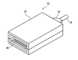
図1は、一実施形態の光トランシーバ10を備える光アクティブケーブル12の構成を概略的に示す斜視図である。光アクティブケーブル12は、1本の光ケーブル14と、光ケーブル14の両端に取り付けられた2個の光トランシーバ10からなる。光アクティブケーブル12は、例えば、スイッチングハブ等の中継装置同士の接続に適用される。
Hereinafter, embodiments of the present invention will be described with reference to the drawings.
FIG. 1 is a perspective view schematically showing a configuration of an optical
図2は、光ケーブル14の一部とともに、光トランシーバ10を拡大して示す斜視図である。
光トランシーバ10は例えば金属製のハウジング16を有し、ハウジング16は例えば箱形状を有する。ハウジング16の一端からは、シール部材18を介して光ケーブル14が延出する一方、ハウジング16の他端には、開口が形成されている。
ハウジング16の開口内には、例えば1枚の回路基板20の端部が位置している。回路基板20の端部は、中継装置に設けられたスロットに挿入可能である。
FIG. 2 is an enlarged perspective view showing the
The
In the opening of the
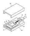
図3は、光トランシーバ10を分解して概略的に示す斜視図であり、ハウジング16は、例えば相互に分離可能な第1ケース16a及び第2ケース16bからなる。
回路基板20は、例えばガラスエポキシ製のリジッドな基板であって、第2ケース16bに対して固定されている。回路基板20には、例えば銅等の金属からなる所定の導体パターンが形成されており、導体パターンは、回路基板20の端部に配置された複数の電極端子22を含む。電極端子22は、中継装置に設けられた電極端子に電気的に接続される。
FIG. 3 is an exploded perspective view schematically showing the
The
また、回路基板20には、電極端子22に電気的に繋がっているコネクタ24が取り付けられており、コネクタ24に、光電変換アセンブリ26の一端が接続されている。
一方、光ケーブル14は、少なくとも1本の光ファイバー28を含み、本実施形態では4本の光ファイバー28を含む。光ファイバー28は、シール部材18を通じて、ハウジング16の内部まで延びている。そして、ハウジング16の内部に位置する光ファイバー28の先端は、光電変換アセンブリ26の他端に固定されている。
Further, a
On the other hand, the
光電変換アセンブリ26は、光ファイバー28から受け取った光信号を電気信号に変換し、電極端子22を通じて中継装置に渡す機能、或いは、中継装置から受け取った電気信号を光信号に変換して光ファイバー28に渡す機能を有する。
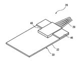
図4は、光電変換アセンブリ26の第2ケース16b側を示す斜視図である。光電変換アセンブリ26は、FPC基板(フレキシブルプリント回路基板)30を含み、FPC基板30は、例えば、ポリイミド製の可撓性及び透光性を有するフィルム32と、フィルム32に設けられた例えば銅等の金属からなる導体パターンとからなる。FPC基板30の導体パターンは、フィルム32の一端部に形成された複数の電極端子34を含む。
なお導体パターンは、例えば、フィルム32に成膜された金属膜をエッチングすることにより作成することができる。
The
FIG. 4 is a perspective view showing the
The conductor pattern can be created, for example, by etching a metal film formed on the
FPC基板30の一方の面には、所定の位置にICチップ36及び光電変換素子38が例えばフリップチップ実装され、ICチップ36及び光電変換素子38は導体パターンに電気的に接続されている。
本実施形態では、光ファイバー28の数に対応して4つの光電変換素子38が実装され、光電変換素子38は、ICチップ36の近傍に沿うように並べられている。各光電変換素子38は、LD(レーザダイオード)等の発光素子又はPD(フォトダイオード)等の受光素子であり、ICチップ36は、発光素子のための駆動回路、又は、受光素子のための増幅回路を構成している。
光電変換素子38は、面発光型若しくは面受光型であり、光電変換素子38は、自身の光の出射面若しくは入射面がFPC基板30の面と対向するように配置されている。
On one surface of the
In the present embodiment, four
The
図5は、図4のICチップ36及び光電変換素子38の周辺を拡大して概略的に示す平面図である。ICチップ36と光電変換素子38とは、導体パターンの一部を構成する電極(第1電極)40a,40bによって電気的に接続されている。そして、ICチップ36は、導体パターンの一部を構成する複数の電極(第2電極)42によって、電極端子34と電気的に接続されている。
FIG. 5 is an enlarged plan view schematically showing the periphery of the
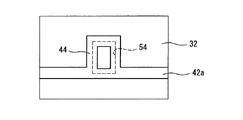
本実施形態では、好ましい態様として、第2電極42のうちの1つのグランド電極42aが、ICチップ36の端から端まで延びている。そして、ICチップ36の中央に対向する位置にて、グランド電極42aには、例えば四角形の枠形状のマーカパターン44が一体に設けられている。マーカパターン44は、第1電極40a,40b及び第2電極42と同様に、導体パターンの一部を構成している。
In the present embodiment, as a preferred mode, one
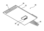
図6は、光電変換アセンブリ26の第1ケース16a側を示す斜視図であり、FPC基板30の他方の面には、電極端子34とは反対側の端部に、シート状のポリマー光導波路部材46が一体に設けられている。
また、FPC基板30の他方の面には、ミラー部材48が接着剤を用いて固定されている。接着剤としては、例えば、熱硬化型樹脂又はUV硬化型樹脂を用いることができる。
FIG. 6 is a perspective view showing the
A
図7は、光電変換アセンブリ26から、ミラー部材48を外した状態を示す概略的な斜視図である。
ポリマー光導波路部材46の端部には、光ファイバー28の数に対応して、ストライプ状に4本の溝が形成され、各溝内に光ファイバー28の先端部が配置されている。
FIG. 7 is a schematic perspective view showing a state in which the
Four grooves are formed in stripes corresponding to the number of
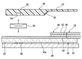
図8は、ミラー部材48のFPC基板30とは反対側を概略的に示す斜視図であり、図9は、ミラー部材48のFPC基板30側を概略的に示す斜視図である。図8及び図9に示したように、ミラー部材48は、相互に一体化された本体部50と張り出し部52とを有する。
FIG. 8 is a perspective view schematically showing the side of the
具体的には、ミラー部材48の本体部50は、四角錐台形状を有し、ミラー部材48の1つの壁面(底壁)は、FPC基板30に沿って密着させられる。FPC基板30の長さ方向及び幅方向での本体部50の長さは、好ましくはICチップ36の長さと同等かそれらよりも長い。
Specifically, the
本体部50の底壁には、好ましい態様として、例えば1つのマーカ凹部54が形成され、マーカ凹部54は、本体部50の底壁の中央付近に位置している。マーカ凹部54は、FPC基板30に向けて開口しており、例えば、平面でみて四角形状を有する。平面でみたときのマーカ凹部54の大きさは、導体パターンのマーカパターン44の大きさに対応しており、好ましくは、マーカ部凹部54の開口の1辺の長さは50μm以上500μm以下であり、開口面積は7500μm2以上250000μm2以下である。また、好ましくは、マーカ凹部54の深さは30μm以上300μm以下である。
As a preferred embodiment, for example, one
張り出し部52側に位置する本体部50の壁面(側壁)は、ミラー面56を構成しており、本体部50の底壁に対して略45°傾いている。従って、ミラー面56は、FPC基板30に対しても略45°傾くことになる。ミラー面56は、溝とは反対側のポリマー光導波路部材46の端面と対向するように配置され、ミラー面56の長手方向は、ポリマー光導波路部材46の端面の長手方向、及び、FPC基板30の幅方向に一致させられている。
The wall surface (side wall) of the
一方、ミラー部材48の張り出し部52は、例えば四角形の板形状をなし、本体部50の側壁の上部から延びている。張り出し部52は、本体部50の底壁とは対向する壁面(天井壁)と平行に延び、FPC基板30と平行に配置されている。
なお、本実施形態で用いられるミラー部材48は、例えば、樹脂を一体成形してから、ミラー面56になる樹脂の壁面に、金等の金属膜を蒸着して製造される。マーカ凹部54は、樹脂を一体成形する時に形成することができる。
On the other hand, the protruding
The
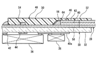
図10は、光電変換アセンブリ26のミラー部材48周辺の縦断面を概略的に示す図である。
ポリマー光導波路部材46は、アンダークラッド層58、コア60、及び、オーバークラッド層62を含む。アンダークラッド層58は、FPC基板30に積層され、光の伝送方向で見て断面形状が四角形のコア60がアンダークラッド層58上を延びている。
FIG. 10 is a diagram schematically showing a longitudinal section around the
The polymer
コア60の数は、光ファイバー28の数に対応して4本であり、4本のコア60は、相互に離間して平行に配置され、光ファイバー28の先端部と同軸上に位置している。オーバークラッド層58は、アンダークラッド層58と協働してコア60を囲むように、アンダークラッド層58及びコア60の上に積層されている。
アンダークラッド層58、コア60、及び、オーバークラッド層62の材料としては、特に限定されることはないが、例えば、アクリル系樹脂、エポキシ系樹脂及びポリイミド系樹脂等を用いることができる。
The number of the
The material of the
本実施形態では、好ましい態様として、アンダークラッド層58が、ミラー面56まで到達するように、フィルム32の表面全域を覆っており、コア60及びオーバークラッド層62が、アンダークラッド層58の端部に積層されている。この場合、アンダークラッド層58が、FPC基板30の表面を構成していると見なすこともできる。
In the present embodiment, as a preferred mode, the under
コア60の両端は、ポリマー光導波路部材46において、溝の端面及びミラー面56と対向する端面にて表出している。そして、コア60の一端は、光ファイバー28の端部と当接して光学的に結合され、コア60の他端は、対向するミラー面56と光学的に結合されている。
Both ends of the core 60 are exposed on the end face of the polymer
また、ミラー部材48は、ミラー面56の位置が、FPC基板30の厚さ方向にて、光電変換素子38の出射面若しくは入射面に対応するように配置されている。つまり、コア60の他端と光電変換素子38との間にて、光路は、ミラー面56によって90°曲げられ、FPC基板30を貫通している。
なおこの配置において、ミラー部材48の本体部50は、FPC基板30の長手方向にて、ICチップ36の端部近傍から光電変換素子38まで延びている。
The
In this arrangement, the
そして本実施形態では、好ましい態様として、アンダークラッド層58上におけるコア60とミラー面56との間には、光導波部材64が設けられている。つまり、コア60とミラー面56との間の光路上には光導波部材64が介在している。
光導波部材64は、好ましくは、ミラー部材48の固定に用いられる接着剤からなり、コア60の端面、ミラー面56及びアンダークラッド層58の表面に密着している。光導波部材64は、透光性を有するのは勿論、アンダークラッド層58及びオーバークラッド層62よりも高い屈折率を有する材料からなり、好ましくは、コア60と同じ屈折率を有する材料からなる。別の表現をすれば、光導波部材64の屈折率は、アンダークラッド層58及びオーバークラッド層62よりも、コア60の屈折率に近い。
また好ましくは、光導波部材64は、コア60の材料と同じ材料からなる。
In the present embodiment, as a preferred mode, an
The
Preferably, the
一方、ミラー部材48の張り出し部52は、ミラー面56の上方からポリマー光導波路部材46に向けて延びている。本実施形態では、好ましい態様として、張り出し部52の長さは、略ポリマー光導波路部材46の長さに等しく、張り出し部52は、溝内に配置された光ファイバー28の先端部を覆っている。そして、張り出し部52は、ポリマー光導波路部材46及び光ファイバー28の先端部に対して、光導波部材64と同じ種類の接着剤(図示せず)にて固定されている。
On the other hand, the protruding
図11は、光電変換アセンブリ26における、マーカ凹部54と、FPC基板30の導体パターンのマーカパターン44との相対的な位置関係を説明するための平面図である。図11に示したように、マーカ凹部54がマーカパターン44に重なるように、ミラー部材48は、FPC基板30に対して位置合わせされている。
FIG. 11 is a plan view for explaining the relative positional relationship between the
なお、ハウジング16内で光電変換アセンブリ26を安定させるために、例えば、回路基板20のコネクタ24側の面には、ガラス板からなる支持部材が配置され、FPC基板30は、例えば、ミラー部材48及び支持部材を介して、第1ケース16a及び回路基板20によって挟持される。
In order to stabilize the
以下、上述した光トランシーバ10の製造に用いられる好ましい方法として、FPC基板30に対してミラー部材48を固定する際に、FPC基板30に対しミラー部材48を位置合わせする方法について説明する。
図12は、位置合わせ方法を説明するための図であり、ステージ66上に配置されたFPC基板30の上方に、図示しない適当なホルダーによって支持されたミラー部材48が配置される。
Hereinafter, as a preferred method used for manufacturing the
FIG. 12 is a view for explaining the alignment method. A
そして、FPC基板30とミラー部材48との間に撮像装置としてカメラ68が配置される。カメラ68は、上方と下方の2つの視野を同時に撮影可能な2視野カメラであり、一方の視野にマーカ凹部54が含まれ、他方の視野にマーカパターン44が含まれる。
それから、カメラ68によって撮影された画像に基づいて、マーカ凹部54とマーカパターン44との相対的な位置関係が予め定められた位置関係になるように、ステージ66又はホルダーが水平方向、即ちFPC基板30と平行な方向に移動させられる。
A
Then, on the basis of the image photographed by the
かくして位置合わせが終了した後、カメラ68をFPC基板30及びミラー部材48から離れるように水平方向に移動させてから、FPC基板30及びポリマー光導波路部材46の所定位置に接着剤を付与する。
そして、ステージ66又はホルダーを上下方向、即ちFPC基板30の厚さ方向に移動させてミラー部材48とFPC基板30とを密着させてから、熱を加えるか若しくは紫外線を照射して、接着剤を硬化させる。これにより、光導波部材64が形成されると同時に、FPC基板30に対するミラー部材48の固定が終了する。
Thus, after the alignment is completed, the
Then, the
上述した一実施形態の光トランシーバ10においては、ミラー部材48が、FPC基板30の表面から、ポリマー光導波路部材46の表面に渡って接着剤で固定されている。ミラー部材48によれば、ミラー部材48の剛性によって、ICチップ36及び光電変換素子38が実装されたFPC基板30の領域が撓むことが防止される。このため、この光トランシーバ10は、ICチップ36及び光電変換素子38と導体パターンとの間の電気的及び機械的な接続部の破壊が防止され、高い信頼性を有する。
また、光トランシーバ10においては、ミラー部材48が補強部材としての機能も有するので、別体の補強部材を省略することができ、部品点数が削減される。
In the
Further, in the
そして、光トランシーバ10においては、ミラー部材48と補強部材の実装が実質的に同時に行われており、補強部材を別工程で実装する必要がない。これにより、この光トランシーバ10によれば、製造工程が削減される。
また、このミラー部材48は、張り出し部52を有することにより大型化が図られているので、取り扱いが容易であり、光トランシーバ10の生産性の向上に寄与する。
In the
In addition, since the
更に、光トランシーバ10においては、張り出し部52が光ファイバー28の先端部にも接着剤を用いて固定されている。これにより、光電変換アセンブリ26に対する光ファイバー28の先端部の接続も補強され、信頼性が更に向上している。そして、光ファイバー28の接続の補強も、1つのミラー部材48を用いて行われており、部品点数及び製造工程が削減されている。
Further, in the
一方、上述した光トランシーバ10においては、アンダークラッド層58がミラー面56の下まで延び、アンダークラッド層58上に、アンダークラッド層58よりも高い屈折率を有する光導波部材64が設けられているので、コア60の端面から出射した光がFPC基板30に向けて拡がることが抑制される。従って、光トランシーバ10においては、コア60の端面から出射した光が効率的にミラー面56に導かれ、コア60と光電変換素子38との間での光の損失が低減される。また、コア60の端面での光の散乱が低減される。
On the other hand, in the
また、上述した一実施形態の光トランシーバ10によれば、その製造工程において、FPC基板30に対してミラー部材48を固定する際、マーカ凹部54とマーカパターン44を目印として用いることによって、FPC基板30に対するミラー部材48の位置合わせが、容易且つ高精度にて行われる。
このため、光トランシーバ10の製造時間が短縮され、ひいては光トランシーバ10の製造コストが削減される。
Further, according to the
For this reason, the manufacturing time of the
また、位置合わせが高精度にて行われる結果、ミラー面56がポリマー光導波路部材46と衝突することが防止される。これによって、衝突によりミラー面56又はポリマー光導波路部材46のコア60の端面が傷付くことが防止され、光電変換アセンブリ26の歩留まりが向上する。この結果としても、光トランシーバ10の製造コストが削減される。
その上、マーカパターン44はグランド電極42aに繋がっているので、マーカパターン44の電位が浮くことがなく、電位が浮くことによる不具合が生じない。
更に、マーカ凹部54は、FPC基板30と対向するミラー部材48の底壁に形成されているので、マーカ凹部54を設けたことによって、ミラー部材48が大型化することはない。
Further, as a result of the alignment being performed with high accuracy, the
In addition, since the
Furthermore, since the
本発明は、上述した一実施形態に限定されることはなく、一実施形態に変更を加えた形態も含む。
例えば、上述した一実施形態の光トランシーバ10では、張り出し部52が四角形の平面形状を有していたが、四角形以外の平面形状を有していてもよい。
The present invention is not limited to the above-described embodiment, and includes a form obtained by modifying the embodiment.
For example, in the
上述した一実施形態の光トランシーバ10では、ミラー部材48の材料は樹脂に限定されることはなく、金属やガラス等を用いてもよい。金属製のミラー部材48によれば、ICチップ36及び光電変換素子38で発生した熱を効率的に逃がすことができ、更に信頼性が向上する。
なお、金属製のミラー部材48は、例えば、鋳造によって製造することができ、この場合も、鋳造時にマーカ凹部54を形成することができる。そして、金属製のミラー部材48の場合、材質によっては、ミラー面56のための金属膜を省略してもよい。
更に、ミラー部材48は、相互に一体化された金属からなる部分と樹脂からなる部分とを含んでいてもよい。この場合、ミラー部材48は、インサートモールドによって製造可能である。
In the
The
Furthermore, the
そして、上述した一実施形態の光トランシーバ10では、好ましい態様として、ミラー部材48の張り出し部52が光ファイバー28の先端部にも接着されていたが、図13に示したミラー部材70を用いてもよい。ミラー部材70は、ミラー部材48に比べて短い張り出し部72を有する。この場合、光ファイバー28の接続の補強は、ミラー部材70とは別の、例えばガラス板や金属板等の補強部材74を用いてもよい。
In the
また、上述した一実施形態の光トランシーバ10では、好ましい態様として、アンダークラッド層58がフィルム32の表面全域に渡って設けられていたが、図14に示したように、アンダークラッド層76が、コア60及びオーバークラッド層62と同じ領域にのみ、即ち、フィルム32の端部にのみ設けられていてもよい。
Moreover, in the
更に、上述した一実施形態の光トランシーバ10では、FPC基板30がフィルム32を含んでいたけれども、図15に示したように、フィルム32を省略し、アンダークラッド層58に直接導体パターンを形成してもよい。換言すれば、フィルム32がアンダークラッド層58としての機能を有していてもよい。つまり、FPC基板30がポリマー光導波路部材46の一部を兼ねていてもよく、FPC基板30は、一方の表面の少なくとも一部にアンダークラッド層を有していればよい。
そこで本明細書では、フィルム32上にアンダークラッド層58が設けられている場合には、フィルム32とアンダークラッド層58を合わせて「基板」というものとし、フィルム32がアンダークラッド層58を兼ねているときには、フィルム32を「基板」という。
Further, in the
Therefore, in the present specification, when the under
また更に、上述した一実施形態の光トランシーバ10では、好ましい態様として、ミラー面56とコア60の端面との間に介在する光導波部材64とコア60の屈折率が同じであったが、異なっていてもよい。また、ミラー面56とコア60の端面との間に何も介在させなくてもよい。
Furthermore, in the
一方、上述した一実施形態の光トランシーバ10では、好ましい態様として、ミラー部材48に1個のマーカ凹部54が形成され、導体パターンにマーカパターン44が形成されていたが、マーカ凹部54及びマーカパターン44を形成しなくてもよい。また、マーカ凹部54及びマーカパターン44を形成する場合、マーカ凹部54及びマーカパターン44の数は1個に限定されることはなく、2個以上であってもよい。
On the other hand, in the
更に、マーカ凹部54及びマーカパターン44の平面形状は、四角形に限定されることはなく他の多角形、円形、若しくは、楕円形であってもよく、特に限定されることはない。
また更に、マーカ凹部54は、レンズ部材48の本体部50の底壁に形成されていたが、天井壁に形成されていてもよい。
Furthermore, the planar shape of the
Furthermore, although the marker recessed
そして、上述した一実施形態の光トランシーバ10の組み立てに際して、1台の2視野カメラにて位置合わせを行ったけれども、2台の1視野カメラを用いてもよい。この場合、2台のカメラのうち1台を、ミラー部材48とFPC基板30との間ではなく、ミラー部材48の上方に配置し、ミラー部材48を天井壁側から撮影するようにしてもよい。
最後に、本発明は、光トランシーバ以外の光モジュールにも適用可能であるのは勿論である。
In the assembly of the
Finally, it goes without saying that the present invention is applicable to optical modules other than optical transceivers.
10 光トランシーバ(光モジュール)
16 ハウジング
20 回路基板
26 光電変換アセンブリ
28 光ファイバー
30 FPC基板
32 フィルム(基板)
36 ICチップ
38 光電変換素子
46 ポリマー光導波路部材
48 ミラー部材
50 本体部
52 張り出し部
56 ミラー面
58 アンダークラッド層(基板)
60 コア
62 オーバークラッド層
10 Optical transceiver (optical module)
16
36
60
Claims (5)
前記アンダークラッド層に沿って延びるコアと、
前記アンダークラッド層と協働して前記コアを囲むオーバークラッド層と、
前記基板に設けられた導体パターンと、
前記基板に対し前記コアとは反対側に固定され、前記導体パターンの一部と電気的に接続された光電変換素子と、
前記コアの端面と前記光電変換素子との間を延びる光路に配置されるミラー面を有し、前記基板に対し前記コアと同じ側に固定されるミラー部材と
を備え、
前記ミラー部材は、前記オーバークラッド層の少なくとも一部を覆う張り出し部を有する、
光モジュール。 A substrate having flexibility and translucency and having an underclad layer on a part of at least one surface;
A core extending along the undercladding layer;
An overclad layer surrounding the core in cooperation with the underclad layer;
A conductor pattern provided on the substrate;
A photoelectric conversion element fixed on the opposite side of the core to the substrate and electrically connected to a part of the conductor pattern;
A mirror surface disposed on an optical path extending between the end face of the core and the photoelectric conversion element, and a mirror member fixed on the same side as the core with respect to the substrate,
The mirror member has an overhanging portion that covers at least a part of the over cladding layer.
Optical module.
前記張り出し部は、前記光ファイバーの端部の少なくとも一部を覆う、
請求項1に記載の光モジュール。 An end of an optical fiber is disposed to be optically coupled to the core;
The overhanging portion covers at least a part of the end of the optical fiber,
The optical module according to claim 1.
前記コアの端面と前記ミラー面との間に、前記アンダークラッド層よりも高い屈折率を有する光導波部材が設けられている、
請求項1乃至3の何れか一項に記載の光モジュール。 The under-cladding layer extends to the mirror surface beyond the end face of the core;
Between the end surface of the core and the mirror surface, an optical waveguide member having a refractive index higher than that of the under cladding layer is provided.
The optical module as described in any one of Claims 1 thru | or 3.
前記導体パターンは、前記ミラー部材に対する位置合わせ用のマーカパターンを含む、
請求項1乃至4の何れか一項に記載の光モジュール。 The mirror member has a recess as a marker for alignment with the substrate,
The conductor pattern includes a marker pattern for alignment with the mirror member,
The optical module as described in any one of Claims 1 thru | or 4.
Priority Applications (1)
| Application Number | Priority Date | Filing Date | Title |
|---|---|---|---|
| JP2011022317A JP5614725B2 (en) | 2011-02-04 | 2011-02-04 | Optical module |
Applications Claiming Priority (1)
| Application Number | Priority Date | Filing Date | Title |
|---|---|---|---|
| JP2011022317A JP5614725B2 (en) | 2011-02-04 | 2011-02-04 | Optical module |
Publications (2)
| Publication Number | Publication Date |
|---|---|
| JP2012163649A true JP2012163649A (en) | 2012-08-30 |
| JP5614725B2 JP5614725B2 (en) | 2014-10-29 |
Family
ID=46843115
Family Applications (1)
| Application Number | Title | Priority Date | Filing Date |
|---|---|---|---|
| JP2011022317A Expired - Fee Related JP5614725B2 (en) | 2011-02-04 | 2011-02-04 | Optical module |
Country Status (1)
| Country | Link |
|---|---|
| JP (1) | JP5614725B2 (en) |
Cited By (3)
| Publication number | Priority date | Publication date | Assignee | Title |
|---|---|---|---|---|
| WO2016063751A1 (en) * | 2014-10-24 | 2016-04-28 | 日東電工株式会社 | Optical/electric hybrid substrate, and production method therefor |
| WO2016063752A1 (en) * | 2014-10-24 | 2016-04-28 | 日東電工株式会社 | Optical/electric hybrid substrate, and production method therefor |
| WO2019078485A1 (en) * | 2017-10-20 | 2019-04-25 | 주식회사 네패스 | Optical module |
Citations (6)
| Publication number | Priority date | Publication date | Assignee | Title |
|---|---|---|---|---|
| JPH0513749A (en) * | 1991-06-28 | 1993-01-22 | Nippon Telegr & Teleph Corp <Ntt> | Optical connection circuit |
| JP2001083373A (en) * | 1999-09-09 | 2001-03-30 | Denso Corp | OPTICAL RECEIVING MODULE AND METHOD OF MANUFACTURING IT AS WELL AS Si CARRIER FOR IT |
| JP2001091771A (en) * | 1999-09-21 | 2001-04-06 | Matsushita Electric Ind Co Ltd | Optical waveguide component and its manufacturing method |
| JP2007212915A (en) * | 2006-02-13 | 2007-08-23 | Seiko Epson Corp | Optoelectric hybrid circuit board and electronic appliance |
| JP2007256298A (en) * | 2004-03-19 | 2007-10-04 | Nec Corp | Optical module and method for manufacturing the same |
| JP2011017933A (en) * | 2009-07-09 | 2011-01-27 | Fujikura Ltd | Optical connector |
-
2011
- 2011-02-04 JP JP2011022317A patent/JP5614725B2/en not_active Expired - Fee Related
Patent Citations (6)
| Publication number | Priority date | Publication date | Assignee | Title |
|---|---|---|---|---|
| JPH0513749A (en) * | 1991-06-28 | 1993-01-22 | Nippon Telegr & Teleph Corp <Ntt> | Optical connection circuit |
| JP2001083373A (en) * | 1999-09-09 | 2001-03-30 | Denso Corp | OPTICAL RECEIVING MODULE AND METHOD OF MANUFACTURING IT AS WELL AS Si CARRIER FOR IT |
| JP2001091771A (en) * | 1999-09-21 | 2001-04-06 | Matsushita Electric Ind Co Ltd | Optical waveguide component and its manufacturing method |
| JP2007256298A (en) * | 2004-03-19 | 2007-10-04 | Nec Corp | Optical module and method for manufacturing the same |
| JP2007212915A (en) * | 2006-02-13 | 2007-08-23 | Seiko Epson Corp | Optoelectric hybrid circuit board and electronic appliance |
| JP2011017933A (en) * | 2009-07-09 | 2011-01-27 | Fujikura Ltd | Optical connector |
Cited By (13)
| Publication number | Priority date | Publication date | Assignee | Title |
|---|---|---|---|---|
| CN107076925A (en) * | 2014-10-24 | 2017-08-18 | 日东电工株式会社 | Optical/electrical mixed mounting substrate and its manufacture method |
| WO2016063752A1 (en) * | 2014-10-24 | 2016-04-28 | 日東電工株式会社 | Optical/electric hybrid substrate, and production method therefor |
| JP2016085314A (en) * | 2014-10-24 | 2016-05-19 | 日東電工株式会社 | Photo-electric hybrid substrate and manufacturing method thereof |
| JP2016085315A (en) * | 2014-10-24 | 2016-05-19 | 日東電工株式会社 | Photo-electric hybrid substrate and manufacturing method thereof |
| CN106796325A (en) * | 2014-10-24 | 2017-05-31 | 日东电工株式会社 | Optical/electrical mixed mounting substrate and its manufacture method |
| KR20170076655A (en) * | 2014-10-24 | 2017-07-04 | 닛토덴코 가부시키가이샤 | Optical/electric hybrid substrate, and production method therefor |
| WO2016063751A1 (en) * | 2014-10-24 | 2016-04-28 | 日東電工株式会社 | Optical/electric hybrid substrate, and production method therefor |
| US10073232B2 (en) | 2014-10-24 | 2018-09-11 | Nitto Denko Corporation | Opto-electric hybrid board, and production method therefor |
| US10353161B2 (en) | 2014-10-24 | 2019-07-16 | Nitto Denko Corporation | Opto-electric hybrid board and method of manufacturing same |
| CN107076925B (en) * | 2014-10-24 | 2020-05-22 | 日东电工株式会社 | Opto-electric hybrid board and method for manufacturing the same |
| CN106796325B (en) * | 2014-10-24 | 2021-07-23 | 日东电工株式会社 | Opto-electric hybrid board and method for manufacturing the same |
| KR102523319B1 (en) * | 2014-10-24 | 2023-04-18 | 닛토덴코 가부시키가이샤 | Optical/electric hybrid substrate, and production method therefor |
| WO2019078485A1 (en) * | 2017-10-20 | 2019-04-25 | 주식회사 네패스 | Optical module |
Also Published As
| Publication number | Publication date |
|---|---|
| JP5614725B2 (en) | 2014-10-29 |
Similar Documents
| Publication | Publication Date | Title |
|---|---|---|
| US8165432B2 (en) | Internal-reflection optical path changing member | |
| JP5184708B1 (en) | Optical module | |
| JP2007271998A (en) | Optical connector and optical module | |
| JP2010122312A (en) | Transmission/reception lens block and optical module using the same | |
| JP2013200550A (en) | Lens component and optical module provided therewith | |
| JP5834964B2 (en) | Optical module | |
| JP2017194565A (en) | Optical communication module and manufacturing method thereof | |
| JP2010122311A (en) | Lens block and optical module using the same | |
| US20150192745A1 (en) | Optical fiber connecter and optical communication module | |
| JP5700297B2 (en) | Cable with photoelectric conversion module | |
| JP5614725B2 (en) | Optical module | |
| KR101256814B1 (en) | All passive aligned optical module and manufacturing method thereof | |
| US8888381B2 (en) | Optical module base and optical module | |
| JP2007072199A (en) | Optical module and optical transmission device | |
| JP2011053717A (en) | Optical path changing connector | |
| JP5737199B2 (en) | Optical module and manufacturing method thereof | |
| JP2009053280A (en) | Optical module | |
| JP5664910B2 (en) | Optical module | |
| JP5614726B2 (en) | Optical module and optical module manufacturing method | |
| JP5899925B2 (en) | Lens parts | |
| JP4607063B2 (en) | Manufacturing method of optical path conversion connector | |
| JP5910080B2 (en) | Optical module | |
| JP2016035484A (en) | Optical module and manufacturing method of optical module | |
| JP6421557B2 (en) | Optical module and optical cable | |
| JP4899762B2 (en) | Photoelectric conversion device |
Legal Events
| Date | Code | Title | Description |
|---|---|---|---|
| A621 | Written request for application examination |
Free format text: JAPANESE INTERMEDIATE CODE: A621 Effective date: 20130419 |
|
| A711 | Notification of change in applicant |
Free format text: JAPANESE INTERMEDIATE CODE: A712 Effective date: 20131101 |
|
| A977 | Report on retrieval |
Free format text: JAPANESE INTERMEDIATE CODE: A971007 Effective date: 20131121 |
|
| A131 | Notification of reasons for refusal |
Free format text: JAPANESE INTERMEDIATE CODE: A131 Effective date: 20131210 |
|
| RD04 | Notification of resignation of power of attorney |
Free format text: JAPANESE INTERMEDIATE CODE: A7424 Effective date: 20131218 |
|
| A521 | Request for written amendment filed |
Free format text: JAPANESE INTERMEDIATE CODE: A523 Effective date: 20140207 |
|
| TRDD | Decision of grant or rejection written | ||
| A01 | Written decision to grant a patent or to grant a registration (utility model) |
Free format text: JAPANESE INTERMEDIATE CODE: A01 Effective date: 20140818 |
|
| R150 | Certificate of patent or registration of utility model |
Ref document number: 5614725 Country of ref document: JP Free format text: JAPANESE INTERMEDIATE CODE: R150 |
|
| A61 | First payment of annual fees (during grant procedure) |
Free format text: JAPANESE INTERMEDIATE CODE: A61 Effective date: 20140831 |
|
| LAPS | Cancellation because of no payment of annual fees |