JP2017194565A - Optical communication module and manufacturing method thereof - Google Patents
Optical communication module and manufacturing method thereof Download PDFInfo
- Publication number
- JP2017194565A JP2017194565A JP2016084672A JP2016084672A JP2017194565A JP 2017194565 A JP2017194565 A JP 2017194565A JP 2016084672 A JP2016084672 A JP 2016084672A JP 2016084672 A JP2016084672 A JP 2016084672A JP 2017194565 A JP2017194565 A JP 2017194565A
- Authority
- JP
- Japan
- Prior art keywords
- optical
- optical waveguide
- circuit board
- light
- semiconductor
- Prior art date
- Legal status (The legal status is an assumption and is not a legal conclusion. Google has not performed a legal analysis and makes no representation as to the accuracy of the status listed.)
- Pending
Links
Images


Abstract
Description
本発明は、光通信モジュール及びその製造方法に関する。 The present invention relates to an optical communication module and a manufacturing method thereof.
近年、クラウドサービスの進展やデータセンタの大規模化に伴い、これらのデータ通信を支える光通信用送受信モジュールの大容量化、小型化、低コスト化が強く望まれている。特に40Gbit/sを超える100Gbit/sや200Gbit/s、ひいては400Gbit/s等においては、伝送速度の高速化のみならず、4波長、8波長といった波長多重技術が必須となってきている。 In recent years, with the advancement of cloud services and the increase in the scale of data centers, it is strongly desired to increase the capacity, size, and cost of optical transmission / reception modules that support these data communications. In particular, at 100 Gbit / s exceeding 200 Gbit / s, 200 Gbit / s, and eventually 400 Gbit / s, wavelength multiplexing techniques such as four wavelengths and eight wavelengths are indispensable as well as increasing the transmission speed.
特許文献1では、波長多重光信号をそれぞれの波長ごとに分離するための光分波器、これらの光信号を集光するための複数のレンズ部品、およびそれぞれの信号光を受光する複数のフォトダイオード(以下、PD)を収容する光通信モジュールが記載されている。しかし特許文献1に係る光通信モジュールでは、反射器と光分波器は一の基板上で互いに離間した状態で実装され、かつ、受光素子は前記一の基板から離れて設けられている。そのため反射器と、光分波器と、受光素子との光学的位置合わせが難しくなる。
In
また、特許文献2では、光通信モジュールの小型化及び長距離化のため、光合分波器と、半導体増幅器(以下、SOA)と、ミラーがモノリシック形成され、その上に面発光レーザー(以下、VCSEL)アレイがフリップチップ実装されていることが記載されている。特許文献2同様に、特許文献3では、VCSELアレイの代わりにPDアレイをフリップチップ実装することで、光通信モジュールが構成されている。しかし特許文献2及び特許文献3に係る光通信モジュールでは、合分波器集積SOAアレイ内にミラーが埋め込まれており、レンズ無しでは、VCSELあるいはPDと合分波器集積SOAアレイとの光学的位置合わせが難しくなる。
In
特許文献4では、半導体光素子と光導波路ミラー部上面とを互いに嵌合する凹凸構造が設けられ、その凹凸構造がレンズ機能を有する光導波路モジュールが記載されている。特許文献4に係る光導波路モジュールの構成は、半導体光素子のレンズ機能を有する凹構造と、光導波路ミラー部上面のレンズ機能を有する凸構造とを互いに嵌合することにより、簡便なパッシブアライメント実装と実装トレランスを確保している。しかし特許文献4に係る光導波路モジュールでは、端面ミラーはクラッド内に埋め込まれているので、凸構造とミラーとの光学的位置合わせが難しくなる。 Patent Document 4 describes an optical waveguide module in which a concavo-convex structure for fitting a semiconductor optical element and an upper surface of an optical waveguide mirror portion to each other is provided, and the concavo-convex structure has a lens function. The configuration of the optical waveguide module according to Patent Document 4 is a simple passive alignment mounting method by fitting a concave structure having a lens function of a semiconductor optical element and a convex structure having a lens function on the upper surface of the optical waveguide mirror part to each other. And mounting tolerance is secured. However, in the optical waveguide module according to Patent Document 4, since the end face mirror is embedded in the clad, it is difficult to optically align the convex structure and the mirror.
特許文献5では、バンドパスフィルタと光導波路で構成される光合分波器が記載されている。特許文献5に係る光合分波器では、光導波路素子と半導体レーザーは端面で結合されている。光導波路素子と半導体レーザーとの光学的位置合わせは、視認可能であるため容易かもしれない。しかし光導波路素子と半導体レーザーとは端面で結合されるため、実装は困難である。 Patent Document 5 describes an optical multiplexer / demultiplexer including a bandpass filter and an optical waveguide. In the optical multiplexer / demultiplexer according to Patent Document 5, the optical waveguide element and the semiconductor laser are coupled at the end face. The optical alignment between the optical waveguide element and the semiconductor laser may be easy because it is visible. However, mounting is difficult because the optical waveguide element and the semiconductor laser are coupled at the end face.
本発明の目的は、半導体光素子の実装を容易にする光通信モジュールを供することである。 An object of the present invention is to provide an optical communication module that facilitates mounting of a semiconductor optical device.
(1)本発明の光通信モジュールは、一端が外側面に位置するようにして光導波路が形成された光回路基板と、前記光導波路の前記一端に達するよう光を出射し、又は前記光導波路の前記一端からの光を受光するよう、前記光回路基板上に搭載されたレンズ機能を有する半導体光素子と、を含み、前記光導波路の前記一端は、前記光回路基板の表面に対して斜交するミラー面として構成され、前記半導体光素子は、前記光導波路の前記一端に対して光を出射することにより前記光導波路に光を入力し、又は前記光導波路の前記一端により反射した光を受光する。 (1) An optical communication module according to the present invention includes an optical circuit board on which an optical waveguide is formed so that one end is positioned on an outer surface, and emits light so as to reach the one end of the optical waveguide, or the optical waveguide A semiconductor optical element having a lens function mounted on the optical circuit board so as to receive light from the one end of the optical waveguide, wherein the one end of the optical waveguide is inclined with respect to the surface of the optical circuit board. It is configured as an intersecting mirror surface, and the semiconductor optical device inputs light to the optical waveguide by emitting light to the one end of the optical waveguide, or reflects light reflected by the one end of the optical waveguide. Receive light.
(2)本発明の光通信モジュールは、一端が外側面に位置するようにして光導波路が形成された光回路基板と、前記光導波路の前記一端に達するよう光を出射し、又は前記光導波路の前記一端からの光を受光するよう、前記光回路基板上に搭載されたレンズ機能を有する半導体光素子と、を含み、前記光導波路の前記一端に対向するよう前記光回路基板上に設けられ、前記半導体光素子により出射される光を該一端に向けて反射し、又は該一端から出射される光を前記半導体光素子に向けて反射するミラーをさらに含む。 (2) The optical communication module of the present invention is an optical circuit board on which an optical waveguide is formed so that one end is located on the outer surface, and emits light so as to reach the one end of the optical waveguide, or the optical waveguide A semiconductor optical element having a lens function mounted on the optical circuit board so as to receive light from the one end of the optical circuit, and provided on the optical circuit board so as to face the one end of the optical waveguide. And a mirror that reflects the light emitted from the semiconductor optical element toward the one end, or reflects the light emitted from the one end toward the semiconductor optical element.
(3)上記(2)の光通信モジュールにおいて、前記光回路基板は、前記光導波路を含む上側層と、該上側層より下側に位置して、前記一端より外方に突出する下側層と、を含み、前記ミラーは、前記下側層における前記突出する部分に取り付けられてよい。 (3) In the optical communication module of (2), the optical circuit board includes an upper layer including the optical waveguide, and a lower layer that is located below the upper layer and protrudes outward from the one end. The mirror may be attached to the protruding portion of the lower layer.
(4)上記(1)乃至(3)のいずれかの光通信モジュールにおいて、前記光導波路は、複数の波長の光が合成された合成光と、前記複数の波長の光の各々である複数の単波長光と、を変換する光変換器に接続され、1の前記単波長光を案内してよい。 (4) In the optical communication module according to any one of the above (1) to (3), the optical waveguide includes a plurality of light beams that are synthesized light beams of a plurality of wavelengths and light beams of the plurality of wavelengths. The single wavelength light may be guided to be connected to an optical converter that converts single wavelength light.
(5)上記(4)に記載の光通信モジュールにおいて、前記光回路基板には、前記光変換器が形成されてよい。 (5) In the optical communication module according to (4), the optical converter may be formed on the optical circuit board.
(6)本発明の光通信モジュールの製造方法は、端が外側面に位置するようにして光導波路が形成され、一端にミラーが形成された光回路基板を準備する工程と、発光または受光する機能を有したレンズを備えた半導体光素子を準備する工程と、レセクタプルとパッケージを準備する工程と、前記光半導体素子を、前記光導波路の前記一端に対して光を出射することにより前記光導波路に光を入力する、又は前記光導波路の前記一端により反射した光を受光するように実装する工程と、前記光導波路を前記パッケージ内に配置する工程と、前記レセクタプルと前記光導波路の前記一端の逆側の他端との間の光学的接続を図る工程と、を含む。 (6) The method of manufacturing an optical communication module of the present invention includes a step of preparing an optical circuit board in which an optical waveguide is formed so that the end is positioned on the outer surface and a mirror is formed on one end, and light emission or light reception is performed. A step of preparing a semiconductor optical device including a lens having a function; a step of preparing a recess pull and a package; and emitting the light from the optical semiconductor device to the one end of the optical waveguide. Mounting to receive light reflected from the one end of the optical waveguide, placing the optical waveguide in the package, and forming the recess pull and the one end of the optical waveguide. And optical connection between the other end on the opposite side.
本発明は、光導波路を光回路基板の端面に到達させ、かつ、ミラーを光回路基板の端面に設けることで、ミラーの位置を外部から視認可能とすることができるので、光回路基板と該光回路基板上の半導体光素子との光学的位置合わせを容易にし得る。また本発明は、半導体光素子を光回路基板上に実装するので、光通信モジュールにおいて、光回路基板上への半導体光素子の実装を容易にすることを可能にする。 In the present invention, since the optical waveguide reaches the end face of the optical circuit board and the mirror is provided on the end face of the optical circuit board, the position of the mirror can be visually recognized from the outside. Optical alignment with the semiconductor optical device on the optical circuit board can be facilitated. In addition, since the semiconductor optical device is mounted on the optical circuit board, the present invention makes it possible to easily mount the semiconductor optical device on the optical circuit board in the optical communication module.
[第1の実施形態]
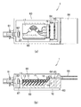
図1(a)は、光通信モジュールの一例の上面図を示している。ここで上面図とは、半導体光素子18が実装される光回路基板17の面が正面に見える図である。図1(b)は、光通信モジュールの一例の断面図を示している。断面は上面に対して垂直にとられている。
[First Embodiment]
FIG. 1A shows a top view of an example of an optical communication module. Here, the top view is a view in which the surface of the
これらの図の光通信モジュール1は、パッケージ63と、パッケージ63の一の端部に取り付けられたレセプタクル61と、パッケージ63の他の端部に取り付けられたフレキシブル基板66と、パッケージ63を封止する蓋69を有する。パッケージ63は、レンズ台67上に設けられたレンズ62と、光回路基板台68に支持された光サブアセンブリ10と、IC台70上に設けられたIC64を内部に含む。
The
光サブアセンブリ10は略垂直な一の端面と斜交する他の端面を有する。一の端面はレンズ62と対向し、他の端面はIC64と対向する。光サブアセンブリ10は、光回路基板17と、光回路基板17上に設けられた半導体光素子18を有する。半導体光素子18にはレンズが設けられている。IC64は、ワイヤーボンディング65によってレンズが設けられた半導体光素子18及びパッケージ63と電気的に接続される。レンズが設けられた半導体光素子18は、光サブアセンブリ10上であって他の端面側に設けられる。
The
これらの図の光通信モジュール1が光送受信機能を実現するため、レセプタクル61、レンズ62、光サブアセンブリ10、及びレンズが設けられた半導体光素子18は光学的に位置合わせされるように配置される。かかる配置では具体的に以下が実現されている。
In order to realize the optical transmission / reception function of the
(1)レセプタクル61へ入射する光が、大きな光学的損失を伴うことなく、レンズ62を通過して光サブアセンブリ10の光導波路へ入射し、端面ミラーである他の端面を介してレンズが設けられた半導体光素子18へ到達する。
(1) The light incident on the
(2)レンズが設けられた半導体光素子18から出射される光が、大きな光学的損失を伴うことなく、端面ミラーである他の端面を介して光サブアセンブリ10の光導波路へ入射し、レンズ62を通過してレセプタクル61から出射する。
(2) The light emitted from the semiconductor
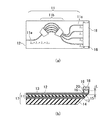
図2(a)は、本発明による光サブアセンブリ10の第1実施例の上面図を示している。図2(b)は、光サブアセンブリ10の第1実施例の断面図を示している。
FIG. 2 (a) shows a top view of a first embodiment of an
本実施例では、光導波路11a、11b、11cと、ミラー15が設けられた光回路基板17上に、レンズ19が設けられた半導体光素子18が実装されている。光導波路11bは、複数の波長の光が合成された合成光と、前記複数の波長の光の各々である複数の単波長光と、を変換する光変換器(光合分波器)であって良い。
In this embodiment, a semiconductor
光サブアセンブリ10は、光回路基板17内に形成される光導波路11と、レンズ19が設けられた半導体光素子18を有する。光導波路11の一端は、光回路基板17の側面に位置、かつ斜交するミラー面を構成する。レンズ19が設けられた半導体光素子18は、ミラー面である光回路基板17の一端へ達するように光を出射して良い。あるいはレンズ19が設けられた半導体光素子18は、光導波路11からミラー面である光回路基板17の一端で反射される光を受光して良い。
The
光回路基板17は、光導波路用基板14の上に光導波路11が形成されている。光導波路11は光導波路コア13の上下を光導波路クラッド12で挟まれた構成となっている。光導波路11は、光導波路11a、11b、11cを含んでいる。さらに光導波路11の上部(上側の光導波路クラッド12上)にレンズ19が設けられた半導体光素子18を実装するための電極16が設けられており、さらに一方の光導波路端面を45度に研磨することによりミラー15を形成されている。光導波路11a、11b、11cは、当業者に周知な任意の方法を用いて形成されて良い。電極16を設ける際、電極16の配置は、レンズ19が設けられた半導体光素子18の受光中心とミラー15で反射する光信号中心とが一致するように行われる。ミラー15は、半導体光素子18が上に実装される面に対して45度の角度をなすことが好ましいが、他の角度であってもよい。
In the
レンズ19が設けられた半導体光素子18は、半導体光素子18の裏面側にレンズ19を形成することによって作成される。レンズ19が設けられた半導体光素子18はモノリシック形成されてよい。レンズ19が設けられた半導体光素子18は、光回路基板17上に形成されている電極16上に半田20を用いて実装される。このときレンズ19は光回路基板17側に配置される。また半導体光素子18への通電は、光回路基板側より行ってもかまないし、レンズ19が形成されていない面側にワイヤ等で通電させても構わない。
The semiconductor
光導波路用基板14はSiで構成されることが好ましいが、石英系ガラス材料、GaAs、InP等の他の基板材料で構成されてもよい。光導波路は石英系で構成されることが好ましいが、ポリマー材料や半導体材料で構成されてもよい。光合分波器11bはアレイ導波路回折格子(以下、AWG)であることが好ましいが、他の種類の光合分波器であってもよい。レンズ19が設けられた半導体光素子18はアレイであることが好ましいが、複数の単体素子であってもよい。またレンズ19が設けられた半導体光素子18はレーザーダイオード(以下、LD)アレイであってもよい。
The
この構成は、レンズ19を半導体光素子18に設け、ミラー15を光回路基板17に設けることで部品点数を減少させている。またこの構成は、レンズ19をレンズが設けられた半導体光素子18の裏面に設けることにより、半導体光素子18の受光中心と裏面レンズ位置とを高い精度で位置合わせすることが可能となる。またこの構成は、光導波路11を光回路基板17の端面に到達させ、かつ、ミラー15を光回路基板17の端面に設けることで、ミラー15の位置を外部から視認可能とすることができるので、光回路基板17と該光回路基板上の半導体光素子18との光学的位置合わせを容易にし得る。結果として、光通信モジュールにおいて、光回路基板17上への半導体光素子18の実装が容易となり得る。さらにこの構成は、実装による簡便なパッシブアライメントを可能にする。またこの構成は、信号光空間伝播距離Lを短くすることで高い結合効率を確保することを可能にする。特にこの信号光空間伝播距離Lを100μm以下にすると効果的である。
In this configuration, the
ここで本実施形態にかかる光通信モジュールの製造方法について説明する。まず光回路基板17の所望の位置に半導体光素子18を実装する。上述したように、光回路基板17の所望の位置に半導体光素子18を例えばパッシブアライメントにて実装するだけで簡便に光回路基板17と半導体光素子18の光学的な接続が得られる。次に、光通信モジュールのパッケージ63内の所定の位置に光回路基板17、IC64を配置する。すなわち、光回路基板17は光回路基板台68を介してパッケージ63の底面に配置され、IC64はIC台70を介してパッケージ63の底面に配置される。この時、半導体光素子18の上面(レンズ19が形成されていない側の面)の高さとIC64の上面の高さの差が極力小さくなるように、光回路基板台68及びIC台70の高さは設定されている。ただし、この高さはこれに限定されることはなく、必要に応じて任意の高さに設定しても構わない。また半導体光素子18を実装する前に、光回路基板17をパッケージ63に配置しても構わない。なおパッケージ63は内部が刳り貫かれた箱状が一般的であり、先に半導体光素子18を実装してから光回路基板17を配置した方が作業性は良い。次に、レンズ62を配置する。この時、この後に組み立てるレセプタクル61の仮想位置と半導体光素子17のミラー17が形成されていない他端との間の光学接続が最適となるようにレンズ62を実装する。そして、蓋69をすることでパッケージ63内部を気密封止する。その後、レセプタクル61を半導体光素子17のミラー17が形成されていない他端との間の光学接続が最適となるように調整し固定する。最後に必要に応じてフレキシブル基板66を設置して光通信モジュールは完成する。以上のように、本実施形態によればアクティブな光学調心は、レセプタクル61の配置時だけであり、複雑な光学的な位置合わせを必要とせずに光通信モジュールを作成することができる。
Here, a method for manufacturing the optical communication module according to the present embodiment will be described. First, the semiconductor
なお、各々の部品配置は上述した順番には限定されない。例えば、半導体光素子18を実装する前に光回路基板17をパッケージ63に配置し、レンズ62を配置しても構わない。ただし、レセプタクル61の調心においては、半導体光素子18が受光素子の場合は、レセプタクル61から入光し半導体光素子18の出力をモニタしながら調整すると作業性が高く、先に半導体光素子18を実装する方が好ましい。さらに、IC64は必要に応じてパッケージ64内に設ければよく、本願発明の必須要件ではない。
In addition, each component arrangement | positioning is not limited to the order mentioned above. For example, the
[第2の実施形態]
図3(a)は、本発明による光サブアセンブリの第2実施例の上面図を示している。図3(b)は、光サブアセンブリの第2実施例の断面図を示している。本実施例は図2の実施例と実質的に同一である。しかし本実施例では、光導波路11a、11b、11cと、光合分波器とミラー15が設けられた光回路基板17と、レンズ19が設けられた半導体光素子18が実装用基板21上に実装されている。光導波路11bは光合分波器を構成して良い。
[Second Embodiment]
FIG. 3 (a) shows a top view of a second embodiment of an optical subassembly according to the present invention. FIG. 3 (b) shows a cross-sectional view of a second embodiment of the optical subassembly. This embodiment is substantially the same as the embodiment of FIG. However, in this embodiment, the
実装用基板21の表面は凸部23と凹部24を有する。凸部23には接着剤22を用いて光回路基板17が実装される。凹部24には電極16が形成され、電極16上にレンズ19が設けられた半導体光素子18が半田20を用いて実装される。このときレンズ19が設けられた半導体光素子18の裏面に作り込まれたレンズ19は光回路基板17上の光導波路に対向する。またレンズ19が設けられた半導体光素子18の受光中心とミラー15で反射する光信号中心が一致するように、光回路基板17は実装される。
The surface of the mounting
光導波路用基板14はSiで構成されることが好ましいが、石英系ガラス材料、GaAs、InP等の他の基板材料で構成されてもよい。光導波路は石英系光導波路であることが好ましいが、ポリマー材料や半導体材料で構成されてもよい。光合分波器はアレイ導波路回折格子(以下、AWG)であることが好ましいが、他の種類の光合分波器であってもよい。
The
レンズが設けられた半導体光素子18はPDアレイであることが好ましいが、複数の単体素子であってもよい。また半導体光素子18はLDアレイであってもよい。
The semiconductor
この構成は、レンズ19を半導体光素子18に設け、ミラー15を光回路基板17に設けることで部品点数を減少させている。またこの構成は、レンズ19をレンズが設けられた半導体光素子18の裏面に設けることにより、半導体光素子18の受光中心と裏面レンズ位置とを高い精度で位置合わせすることが可能となる。またこの構成は、光導波路を光回路基板の端面に到達させ、かつ、ミラー15を光回路基板17の端面に設けることで、ミラー15の位置を外部から視認可能とすることができるので、光回路基板17と該光回路基板上の半導体光素子18との光学的位置合わせを容易にし得る。結果として、光通信モジュールにおいて、光回路基板17上への半導体光素子18の実装が容易となり得る。さらにこの構成は、簡便なパッシブアライメントを可能にする。
In this configuration, the
本実施例ではレンズ19が設けられた半導体光素子18としてPDアレイを例示したがアレイではなく複数の単体素子が使用されてもよい。さらにはPDではなくレンズが設けられた面出射型のLDが用いられてもよい。
In the present embodiment, a PD array is exemplified as the semiconductor
本実施例ではCWDM(Coarse Wavelength Division Multiplexing)に対応した4波長が例示されているが、LANWDM(Local Area Network Wavelength Division Multiplexing)やDWDM(Dense Wavelength Division Multiplexing)等のWDMが用いられてもよく、また2波長以上の複数の波長数が用いられてもよい。 In this embodiment, four wavelengths corresponding to CWDM (Coarse Wavelength Division Multiplexing) are exemplified, but WDM such as LAN WDM (Local Area Network Wavelength Division Multiplexing) and DWDM (Dense Wavelength Division Multiplexing) may be used. A plurality of wavelengths of two or more wavelengths may be used.
[第3の実施形態]
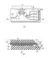
図4(a)は、光サブアセンブリの第3実施例の上面図を示している。図4(b)は、光サブアセンブリの第3実施例の断面図を示している。本実施例は図2の実施例と実質的に同一である。しかし図2の実施例ではミラー15は光回路基板17の導波路端面を45度に研磨することにより形成されているが、本実施例では、光回路基板32上に別部品のミラー31が搭載されている。
[Third Embodiment]
FIG. 4 (a) shows a top view of a third embodiment of the optical subassembly. FIG. 4B shows a cross-sectional view of a third embodiment of the optical subassembly. This embodiment is substantially the same as the embodiment of FIG. However, in the embodiment of FIG. 2, the
本実施例の光サブアセンブリは、光導波路11を含む上側層及び該上側層より下側に位置して一端より右側に突出する下側層を有する光回路基板32と、前記下側層の突出する部分の上に設けられるミラー31と、光導波路11とミラー31の上に実装されたレンズ19が設けられた半導体光素子18を有する。光導波路11の一端は光回路基板32の側面に位置する。レンズ19が設けられた半導体光素子18は、電極16を用いてフリップフロップ実装されてよい。レンズ19が設けられた半導体光素子18は、ミラー31へ達するように光を出射して良い。あるいはレンズ19が設けられた半導体光素子18は、光導波路11からミラー31で反射される光を受光しても良い。
The optical subassembly of the present embodiment includes an
光回路基板32は、光導波路11a、11b、11cが光導波路用基板14上の一部に形成し、光導波路用基板14上の光導波路11が設けられていない領域上にミラー31を設けられることによって形成されてよい。光導波路11a、11b、11cは、当業者に周知な任意の方法を用いて形成されて良い。電極16を設ける際、電極16の配置は、レンズ19が設けられた半導体光素子18の受光中心とミラー15で反射する光信号中心とが一致するように行われる。
In the
本実施例では、信号光空間伝播距離はL1+L2で表される。またミラー31は、光導波路11の端面に対して45度の角度をなすことが好ましいが、他の角度であってもよい。
In this embodiment, the signal light space propagation distance is represented by L 1 + L 2 . The
[第4の実施形態]
図5(a)は、光サブアセンブリの第4実施例の上面図を示している。図5(b)は、光サブアセンブリの第4実施例の断面図を示している。本実施例は図2の実施例と実質的に同一である。しかし図2の実施例では、半導体光素子18は、半田20を用いて光回路基板17上の電極16にフリップチップ実装されているが、本実施例では、半田20の代わりに透明樹脂41によってレンズ19が設けられた半導体光素子18が実装されている。透明樹脂41はUV硬化接着剤等であってよい。
[Fourth Embodiment]
FIG. 5 (a) shows a top view of a fourth embodiment of the optical subassembly. FIG. 5 (b) shows a cross-sectional view of a fourth embodiment of the optical subassembly. This embodiment is substantially the same as the embodiment of FIG. However, in the embodiment of FIG. 2, the semiconductor
[第5の実施形態]
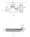
図6(a)は、光サブアセンブリの第5実施例の上面図を示している。図6(b)は、光サブアセンブリの第5実施例の断面図を示している。本実施例は図2乃至図5の実施例と実質的に同一である。しかし図2乃至図5の実施例では、光合分波器としてAWGが用いられているが、本実施例の光合分波器51は、ミラー53と、4つのフィルタ54と、光導波路11bを有する。
[Fifth Embodiment]
FIG. 6A shows a top view of the fifth embodiment of the optical subassembly. FIG. 6B shows a cross-sectional view of a fifth embodiment of the optical subassembly. This embodiment is substantially the same as the embodiment shown in FIGS. However, although the AWG is used as the optical multiplexer / demultiplexer in the embodiments of FIGS. 2 to 5, the optical multiplexer /
光合分波器51は、光回路基板55に2つの溝52を設け、溝52のうちの一方にミラー53を挿入し、その後、溝52のうちの他方に各波長に対応する4つのバンドパスフィルタ54を挿入することによって形成される。さらにはエシェルグレーティング等の回折格子用いた光合分波器が、光合分波器51として用いられてもよい。
The optical multiplexer /
また、本実施例ではレンズ19が設けられた半導体光素子18としてPDアレイが例示されているがアレイに限定されず、複数の単体素子が用いられてもよい。さらに、PDではなくレンズを設けた面出射型のLDを用いて送信光アセンブリが構成されてもよい。
In the present embodiment, a PD array is illustrated as the semiconductor
光導波路用基板14はSiで構成されることが好ましいが、石英系ガラス材料、GaAs、InP等の他の基板材料で構成されてもよい。光導波路は石英系で構成されることが好ましいが、ポリマー材料や半導体材料で構成されてもよい。
The
本実施例ではCWDM(Coarse Wavelength Division Multiplexing)に対応した4波長が例示されているが、LANWDM(Local Area Network Wavelength Division Multiplexing)やDWDM(Dense Wavelength Division Multiplexing)等のWDMを用いても同様であり、また波長数も2波長以上の複数波長であれば同等である。 In this embodiment, four wavelengths corresponding to CWDM (Coarse Wavelength Division Multiplexing) are illustrated, but the same applies even when WDM such as LAN WDM (Local Area Network Wavelength Division Multiplexing) or DWDM (Dense Wavelength Division Multiplexing) is used. Further, the number of wavelengths is the same as long as it is a plurality of wavelengths of two or more wavelengths.
1 光通信モジュール、10 光サブアセンブリ、11 光導波路、12 光導波路クラッド、13 光導波路コア、14 光導波路用基板、15 ミラー、16 電極、17 光回路基板、18 半導体光素子、19 レンズ、20 半田、21 実装用基板、22 接着剤、23 凸部、24 凹部、31 ミラー、32 光回路基板、41 透明樹脂、51 光合分波器、52 溝、53 ミラー、54 バンドパスフィルタ、55 光回路基板、61 レセプタクル、62 レンズ、63 パッケージ、64 IC、65 ワイヤーボンディング、66 フレキシブル基板、67 レンズ台、68 光回路基板台、69 蓋、70 IC台。
DESCRIPTION OF
Claims (6)
前記光導波路の前記一端に達するよう光を出射し、又は前記光導波路の前記一端からの光を受光するよう、前記光回路基板上に搭載されたレンズ機能を有する半導体光素子と、
を含み、
前記光導波路の前記一端は、前記光回路基板の表面に対して斜交するミラー面として構成され、
前記半導体光素子は、前記光導波路の前記一端に対して光を出射することにより前記光導波路に光を入力し、又は前記光導波路の前記一端により反射した光を受光する、
光通信モジュール。 An optical circuit board on which an optical waveguide is formed so that one end is located on the outer surface;
A semiconductor optical element having a lens function mounted on the optical circuit board so as to emit light to reach the one end of the optical waveguide, or to receive light from the one end of the optical waveguide;
Including
The one end of the optical waveguide is configured as a mirror surface oblique to the surface of the optical circuit board,
The semiconductor optical element inputs light into the optical waveguide by emitting light to the one end of the optical waveguide, or receives light reflected by the one end of the optical waveguide.
Optical communication module.
前記光導波路の前記一端に達するよう光を出射し、又は前記光導波路の前記一端からの光を受光するよう、前記光回路基板上に搭載されたレンズ機能を有する半導体光素子と、
を含み、
前記光導波路の前記一端に対向するよう前記光回路基板上に設けられ、前記半導体光素子により出射される光を該一端に向けて反射し、又は該一端から出射される光を前記半導体光素子に向けて反射するミラーをさらに含む、
光通信モジュール。 An optical circuit board on which an optical waveguide is formed so that one end is located on the outer surface;
A semiconductor optical element having a lens function mounted on the optical circuit board so as to emit light to reach the one end of the optical waveguide, or to receive light from the one end of the optical waveguide;
Including
Provided on the optical circuit board so as to face the one end of the optical waveguide, reflects light emitted from the semiconductor optical element toward the one end, or reflects light emitted from the one end to the semiconductor optical element Further including a mirror reflecting toward
Optical communication module.
前記光回路基板は、前記光導波路を含む上側層と、該上側層より下側に位置して、前記一端より外方に突出する下側層と、を含み、
前記ミラーは、前記下側層における前記突出する部分に取り付けられる、
光通信モジュール。 The optical communication module according to claim 2,
The optical circuit board includes an upper layer including the optical waveguide, and a lower layer that is located below the upper layer and protrudes outward from the one end,
The mirror is attached to the protruding portion of the lower layer;
Optical communication module.
前記光導波路は、複数の波長の光が合成された合成光と、前記複数の波長の光の各々である複数の単波長光と、を変換する光変換器に接続され、1の前記単波長光を案内する、
光通信モジュール。 The optical communication module according to any one of claims 1 to 3,
The optical waveguide is connected to an optical converter that converts combined light obtained by combining light of a plurality of wavelengths and a plurality of single wavelength lights that are each of the light of the plurality of wavelengths. Guide the light,
Optical communication module.
前記光回路基板には、前記光変換器が形成される、
光通信モジュール。 The optical communication module according to claim 4,
The optical converter is formed on the optical circuit board.
Optical communication module.
発光または受光する機能を有したレンズを備えた半導体光素子を準備する工程と、
レセクタプルを有するパッケージを準備する工程と、
前記光半導体素子を、前記光導波路の前記一端に対して光を出射することにより前記光導波路に光を入力する、又は前記光導波路の前記一端により反射した光を受光するように実装する工程と、
前記光導波路を前記パッケージ内に配置する工程と、
前記レセクタプルと前記光導波路の前記一端の逆側の他端との間の光学的接続を図る工程と、を含む
光通信モジュールの製造方法。 A step of preparing an optical circuit board in which an optical waveguide is formed so that the end is located on the outer surface and a mirror is formed on one end;
Preparing a semiconductor optical device including a lens having a function of emitting or receiving light;
Preparing a package having a recessive pull;
Mounting the optical semiconductor element so as to input light to the optical waveguide by emitting light to the one end of the optical waveguide, or to receive light reflected by the one end of the optical waveguide; ,
Arranging the optical waveguide in the package;
And a step of optical connection between the less sector pull and the other end opposite to the one end of the optical waveguide.
Priority Applications (1)
| Application Number | Priority Date | Filing Date | Title |
|---|---|---|---|
| JP2016084672A JP2017194565A (en) | 2016-04-20 | 2016-04-20 | Optical communication module and manufacturing method thereof |
Applications Claiming Priority (1)
| Application Number | Priority Date | Filing Date | Title |
|---|---|---|---|
| JP2016084672A JP2017194565A (en) | 2016-04-20 | 2016-04-20 | Optical communication module and manufacturing method thereof |
Related Child Applications (1)
| Application Number | Title | Priority Date | Filing Date |
|---|---|---|---|
| JP2020176563A Division JP2021009413A (en) | 2020-10-21 | 2020-10-21 | Optical communication module and manufacturing method thereof |
Publications (1)
| Publication Number | Publication Date |
|---|---|
| JP2017194565A true JP2017194565A (en) | 2017-10-26 |
Family
ID=60156039
Family Applications (1)
| Application Number | Title | Priority Date | Filing Date |
|---|---|---|---|
| JP2016084672A Pending JP2017194565A (en) | 2016-04-20 | 2016-04-20 | Optical communication module and manufacturing method thereof |
Country Status (1)
| Country | Link |
|---|---|
| JP (1) | JP2017194565A (en) |
Cited By (8)
| Publication number | Priority date | Publication date | Assignee | Title |
|---|---|---|---|---|
| JP2019165128A (en) * | 2018-03-20 | 2019-09-26 | 日本電気株式会社 | Optical module package and optical module package mounting method |
| JP2020071238A (en) * | 2018-10-29 | 2020-05-07 | 日本電信電話株式会社 | Wavelength checker |
| WO2020105472A1 (en) * | 2018-11-22 | 2020-05-28 | 日本電信電話株式会社 | Wavelength checker |
| WO2021038630A1 (en) * | 2019-08-23 | 2021-03-04 | 日本電信電話株式会社 | Wavelength checker |
| JPWO2021095231A1 (en) * | 2019-11-15 | 2021-05-20 | ||
| JP2021077711A (en) * | 2019-11-06 | 2021-05-20 | 住友電気工業株式会社 | Optical module |
| JPWO2021095165A1 (en) * | 2019-11-13 | 2021-05-20 | ||
| WO2022259518A1 (en) * | 2021-06-11 | 2022-12-15 | 日本電信電話株式会社 | Packaging structure for optical waveguide device |
Citations (6)
| Publication number | Priority date | Publication date | Assignee | Title |
|---|---|---|---|---|
| JPH11326662A (en) * | 1998-05-18 | 1999-11-26 | Nec Corp | Optical planar circuit |
| JP2000241642A (en) * | 1999-02-17 | 2000-09-08 | Sumitomo Electric Ind Ltd | Light transmit/receive module |
| JP2000332301A (en) * | 1999-05-19 | 2000-11-30 | Nippon Telegr & Teleph Corp <Ntt> | Semiconductor device having input/output mechanism for optical signal, and manufacture thereof |
| JP2003215371A (en) * | 2002-01-25 | 2003-07-30 | Nec Corp | Optical module and mounting method therefor |
| JP2005266657A (en) * | 2004-03-22 | 2005-09-29 | Sony Corp | Optical waveguide, optical waveguide device, and optical information processing apparatus |
| US20120114293A1 (en) * | 2010-11-05 | 2012-05-10 | Electronics And Telecommunications Research Institute | Optical waveguide structure having angled mirror and lens |
-
2016
- 2016-04-20 JP JP2016084672A patent/JP2017194565A/en active Pending
Patent Citations (6)
| Publication number | Priority date | Publication date | Assignee | Title |
|---|---|---|---|---|
| JPH11326662A (en) * | 1998-05-18 | 1999-11-26 | Nec Corp | Optical planar circuit |
| JP2000241642A (en) * | 1999-02-17 | 2000-09-08 | Sumitomo Electric Ind Ltd | Light transmit/receive module |
| JP2000332301A (en) * | 1999-05-19 | 2000-11-30 | Nippon Telegr & Teleph Corp <Ntt> | Semiconductor device having input/output mechanism for optical signal, and manufacture thereof |
| JP2003215371A (en) * | 2002-01-25 | 2003-07-30 | Nec Corp | Optical module and mounting method therefor |
| JP2005266657A (en) * | 2004-03-22 | 2005-09-29 | Sony Corp | Optical waveguide, optical waveguide device, and optical information processing apparatus |
| US20120114293A1 (en) * | 2010-11-05 | 2012-05-10 | Electronics And Telecommunications Research Institute | Optical waveguide structure having angled mirror and lens |
Cited By (20)
| Publication number | Priority date | Publication date | Assignee | Title |
|---|---|---|---|---|
| JP2019165128A (en) * | 2018-03-20 | 2019-09-26 | 日本電気株式会社 | Optical module package and optical module package mounting method |
| JP7187790B2 (en) | 2018-03-20 | 2022-12-13 | 日本電気株式会社 | Optical module package and optical module package mounting method |
| JP2020071238A (en) * | 2018-10-29 | 2020-05-07 | 日本電信電話株式会社 | Wavelength checker |
| WO2020090433A1 (en) * | 2018-10-29 | 2020-05-07 | 日本電信電話株式会社 | Wavelength checker |
| JP7124638B2 (en) | 2018-10-29 | 2022-08-24 | 日本電信電話株式会社 | wavelength checker |
| JP7099279B2 (en) | 2018-11-22 | 2022-07-12 | 日本電信電話株式会社 | Wavelength checker |
| WO2020105472A1 (en) * | 2018-11-22 | 2020-05-28 | 日本電信電話株式会社 | Wavelength checker |
| JP2020086081A (en) * | 2018-11-22 | 2020-06-04 | 日本電信電話株式会社 | Wavelength checker |
| WO2021038630A1 (en) * | 2019-08-23 | 2021-03-04 | 日本電信電話株式会社 | Wavelength checker |
| US20220276435A1 (en) * | 2019-08-23 | 2022-09-01 | Nippon Telegraph And Telephone Corporation | Wavelength Checker |
| JPWO2021038630A1 (en) * | 2019-08-23 | 2021-03-04 | ||
| JP7215584B2 (en) | 2019-08-23 | 2023-01-31 | 日本電信電話株式会社 | wavelength checker |
| US11747557B2 (en) * | 2019-08-23 | 2023-09-05 | Nippon Telegraph And Telephone Corporation | Wavelength checker |
| JP2021077711A (en) * | 2019-11-06 | 2021-05-20 | 住友電気工業株式会社 | Optical module |
| JP7287242B2 (en) | 2019-11-06 | 2023-06-06 | 住友電気工業株式会社 | optical module |
| JPWO2021095165A1 (en) * | 2019-11-13 | 2021-05-20 | ||
| JP7215593B2 (en) | 2019-11-13 | 2023-01-31 | 日本電信電話株式会社 | wavelength checker |
| JPWO2021095231A1 (en) * | 2019-11-15 | 2021-05-20 | ||
| JP7215595B2 (en) | 2019-11-15 | 2023-01-31 | 日本電信電話株式会社 | wavelength checker |
| WO2022259518A1 (en) * | 2021-06-11 | 2022-12-15 | 日本電信電話株式会社 | Packaging structure for optical waveguide device |
Similar Documents
| Publication | Publication Date | Title |
|---|---|---|
| JP2017194565A (en) | Optical communication module and manufacturing method thereof | |
| US10466433B2 (en) | Optical module including silicon photonics chip and coupler chip | |
| KR101144665B1 (en) | Wavelengh Division Multiplexer and Demultiplexer | |
| JP5563167B2 (en) | Optical communication module | |
| US8540437B2 (en) | Multi-wavelength optical transmitting and receiving modules | |
| US6937786B2 (en) | Parallel multiwavelength optical subassembly | |
| US7773836B2 (en) | Integrated transceiver with lightpipe coupler | |
| KR101925476B1 (en) | optical module and optical engine having the same | |
| US9470846B2 (en) | Wavelength division multiplexing with multi-core fiber | |
| TWI675229B (en) | Optical module including silicon photonics chip and coupler chip | |
| US20160349470A1 (en) | Hybrid integrated optical sub-assembly | |
| JP2007264033A (en) | Optical module, optical transmission system, and manufacturing method of optical module | |
| KR20200111250A (en) | Multi channel optical coupler | |
| US20120213527A1 (en) | Optoelectronic device for bidirectionally transporting information through optical fibers and method of manufacturing such a device | |
| US20060013541A1 (en) | Optoelectronic module | |
| US20050084217A1 (en) | Optical module capable of transmitting optical signal in bi-directional with single fiber | |
| JP5980193B2 (en) | Optical module and optical module manufacturing method. | |
| JP5277389B2 (en) | Optical module | |
| JP2021009413A (en) | Optical communication module and manufacturing method thereof | |
| JP2008020721A (en) | Parallel optical transmitter-receiver | |
| JP4894579B2 (en) | Lens housing and optical module | |
| JP2008096490A (en) | Light receiving assembly | |
| KR101769034B1 (en) | optical engine | |
| JP2003021737A (en) | Optical coupling structure of optical waveguide and light receiving element | |
| JP2009200448A (en) | Wavelength separation photodiode and manufacturing method thereof, and optical module using wavelength separation photodiode |
Legal Events
| Date | Code | Title | Description |
|---|---|---|---|
| A621 | Written request for application examination |
Free format text: JAPANESE INTERMEDIATE CODE: A621 Effective date: 20190117 |
|
| A977 | Report on retrieval |
Free format text: JAPANESE INTERMEDIATE CODE: A971007 Effective date: 20191212 |
|
| A131 | Notification of reasons for refusal |
Free format text: JAPANESE INTERMEDIATE CODE: A131 Effective date: 20191217 |
|
| A521 | Request for written amendment filed |
Free format text: JAPANESE INTERMEDIATE CODE: A523 Effective date: 20200212 |
|
| A02 | Decision of refusal |
Free format text: JAPANESE INTERMEDIATE CODE: A02 Effective date: 20200721 |
|
| A521 | Request for written amendment filed |
Free format text: JAPANESE INTERMEDIATE CODE: A523 Effective date: 20201021 |
|
| C60 | Trial request (containing other claim documents, opposition documents) |
Free format text: JAPANESE INTERMEDIATE CODE: C60 Effective date: 20201021 |
|
| A911 | Transfer to examiner for re-examination before appeal (zenchi) |
Free format text: JAPANESE INTERMEDIATE CODE: A911 Effective date: 20201028 |
|
| C21 | Notice of transfer of a case for reconsideration by examiners before appeal proceedings |
Free format text: JAPANESE INTERMEDIATE CODE: C21 Effective date: 20201104 |
|
| A912 | Re-examination (zenchi) completed and case transferred to appeal board |
Free format text: JAPANESE INTERMEDIATE CODE: A912 Effective date: 20210108 |
|
| C211 | Notice of termination of reconsideration by examiners before appeal proceedings |
Free format text: JAPANESE INTERMEDIATE CODE: C211 Effective date: 20210119 |
|
| C22 | Notice of designation (change) of administrative judge |
Free format text: JAPANESE INTERMEDIATE CODE: C22 Effective date: 20210216 |
|
| C23 | Notice of termination of proceedings |
Free format text: JAPANESE INTERMEDIATE CODE: C23 Effective date: 20210413 |
|
| C03 | Trial/appeal decision taken |
Free format text: JAPANESE INTERMEDIATE CODE: C03 Effective date: 20210511 |
|
| C30A | Notification sent |
Free format text: JAPANESE INTERMEDIATE CODE: C3012 Effective date: 20210511 |