JP2012160845A - Imaging apparatus - Google Patents
Imaging apparatus Download PDFInfo
- Publication number
- JP2012160845A JP2012160845A JP2011018200A JP2011018200A JP2012160845A JP 2012160845 A JP2012160845 A JP 2012160845A JP 2011018200 A JP2011018200 A JP 2011018200A JP 2011018200 A JP2011018200 A JP 2011018200A JP 2012160845 A JP2012160845 A JP 2012160845A
- Authority
- JP
- Japan
- Prior art keywords
- unit
- voltage
- input terminal
- comparison
- pixel
- Prior art date
- Legal status (The legal status is an assumption and is not a legal conclusion. Google has not performed a legal analysis and makes no representation as to the accuracy of the status listed.)
- Granted
Links
Images


Classifications
-
- H—ELECTRICITY
- H04—ELECTRIC COMMUNICATION TECHNIQUE
- H04N—PICTORIAL COMMUNICATION, e.g. TELEVISION
- H04N25/00—Circuitry of solid-state image sensors [SSIS]; Control thereof
- H04N25/70—SSIS architectures; Circuits associated therewith
- H04N25/71—Charge-coupled device [CCD] sensors; Charge-transfer registers specially adapted for CCD sensors
- H04N25/75—Circuitry for providing, modifying or processing image signals from the pixel array
-
- H—ELECTRICITY
- H04—ELECTRIC COMMUNICATION TECHNIQUE
- H04N—PICTORIAL COMMUNICATION, e.g. TELEVISION
- H04N25/00—Circuitry of solid-state image sensors [SSIS]; Control thereof
- H04N25/60—Noise processing, e.g. detecting, correcting, reducing or removing noise
- H04N25/67—Noise processing, e.g. detecting, correcting, reducing or removing noise applied to fixed-pattern noise, e.g. non-uniformity of response
- H04N25/671—Noise processing, e.g. detecting, correcting, reducing or removing noise applied to fixed-pattern noise, e.g. non-uniformity of response for non-uniformity detection or correction
- H04N25/677—Noise processing, e.g. detecting, correcting, reducing or removing noise applied to fixed-pattern noise, e.g. non-uniformity of response for non-uniformity detection or correction for reducing the column or line fixed pattern noise
Landscapes
- Engineering & Computer Science (AREA)
- Multimedia (AREA)
- Signal Processing (AREA)
- Transforming Light Signals Into Electric Signals (AREA)
Abstract
Description
本発明は、撮像装置に関する。 The present invention relates to an imaging apparatus.
従来例に係るAD変換方法を用いた撮像装置として、特許文献1に記載された構成が知られている。初めに、特許文献1に記載された撮像装置の構成および動作について説明する。
As an imaging apparatus using an AD conversion method according to a conventional example, a configuration described in
図18は、特許文献1に記載された従来例に係るAD変換方法を用いた(C)MOS撮像装置の概略構成を示している。撮像装置1001は、撮像部1002、垂直選択部1012、読出し電流源部1005、アナログ部1006、カラム処理部1015、参照信号生成部1016、水平選択部1014、出力部1017、変更部1018、タイミング制御部1020で構成されている。
FIG. 18 shows a schematic configuration of a (C) MOS imaging device using the AD conversion method according to the conventional example described in
タイミング制御部1020は、垂直選択部1012、読出し電流源部1005、アナログ部1006、カラム処理部1015、参照信号生成部1016、水平選択部1014、および出力部1017などの各部を制御する。撮像部1002は、光電変換素子を有する単位画素1003が行列状に配置されて構成され、入射される電磁波の大きさに応じた画素信号を生成し、列毎に設けられた垂直信号線1013へ出力する。
The
垂直選択部1012は、撮像部1002の各単位画素1003の駆動に際して、行制御線1011を介して撮像部1002の行アドレスや行走査の制御を行う。水平選択部1014は、カラム処理部1015の列AD変換部1030の列アドレスや列走査の制御を行う。読出し電流源部1005は、撮像部1002からの画素信号を電圧信号として読み出すための電流源である。アナログ部1006は、必要に応じて増幅等を実施する。
The
カラム処理部1015は、変更部1018と、撮像部1002の列毎に設けられた列AD変換部1030とを有する。変更部1018は、ON(活性化)されることで、所定の電圧を供給する電圧源に短絡される。列AD変換部1030は、撮像部1002の各単位画素1003から列毎に出力される画素信号であるアナログ信号をデジタルデータに変換して出力する。参照信号生成部1016は、例えば積分回路やDAC回路で構成され、時間が経過するにつれて傾斜状に変化する参照信号Rampを生成する。
The
次に、列AD変換部1030の構成について説明する。図19は、列AD変換部1030を含むカラム処理部1015の構成を示している。列AD変換部1030は全て同一に構成され、各々の列AD変換部1030は、比較部1031、計測部1032を有する構成となっている。
Next, the configuration of the column
比較部1031は、一般的に良く知られている差動アンプを基本構成とするコンパレータ回路である。比較部1031は、撮像部1002の単位画素1003から出力される画素信号と参照信号Rampとを比較し、例えば参照信号Rampが画素信号よりも大なるときはHighレベル、例えば参照信号Rampが画素信号よりも小なるときはLowレベルを出力する。
The
計測部1032は、アップ/ダウンカウンタ回路で構成され、比較部1031が比較を開始してから比較を終了するまでの比較時間を計測する。これにより、画素信号の大きさに応じた比較時間の計測値が得られる。水平選択部1014は、シフトレジスタやデコーダなどによって構成され、カラム処理部1015における各列AD変換部1030の列アドレスや列走査の制御を行う。これにより、AD変換されたデジタルデータは順に水平信号線を経由して出力部1017に出力される。
The
比較部1031による比較動作は、比較部1031を構成する差動アンプの2つの入力端の電圧のリセット(バランス)が行われた後に開始される。リセット動作後に、比較部1031を構成する差動アンプの2つの入力端の電圧に多少のばらつきが残ることにより、比較部1031の出力が反転しなかったり、参照信号Rampの入力後直ちに比較部1031の出力が反転したりする不具合を防ぐため、撮像装置1001に変更部1018が設けられている。
The comparison operation by the
次に、AD変換動作について説明する。単位画素1003の具体的な動作については説明を省略するが、単位画素1003からは画素信号としてリセットレベルと信号レベルとが出力される。
Next, the AD conversion operation will be described. Although the description of the specific operation of the
まず、単位画素1003からのリセットレベルの読出しが安定した後、比較部1031を構成する差動アンプの2つの入力端の電圧のリセット(バランス)が行われる。続いて、変更部1018により、参照信号Rampが与えられた入力端に所定の電圧が印加される。その後、比較部1031は、その所定の電圧を比較開始の電圧として参照信号Rampと画素信号との比較を行う。計測部1032はダウンカウントモードで計測を実施し、比較終了時点の計測値がリセットレベルのデジタルデータとなる。
First, after the reset level read from the
続いて、単位画素1003からの信号レベルの読出し時には、比較部1031におけるリセット動作および変更部1018による変更動作は行わない。単位画素1003からの信号レベルの読出しが安定した後、比較部1031は、上記所定の電圧を比較開始の電圧として参照信号Rampと画素信号との比較を行う。計測部1032はアップカウントモードで計測を実施し、比較終了時点の計測部1032の計測値が信号成分(信号レベルからリセットレベルを減算した信号)のデジタルデータとなる。
Subsequently, when the signal level is read from the
以上のように、画素信号をAD変換することが可能となる。また、リセット動作後に、比較部1031を構成する差動アンプの2つの入力端の電圧に多少のばらつきが残ったとしても、変更部1018により、参照信号Rampが与えられた入力端に所定の電圧を印加することで、参照信号Rampが与えられた入力端の電圧が、画素信号が与えられた入力端の電圧よりも高くなるため、比較部1031の出力を比較動作中に確実に反転させることができる。
As described above, the pixel signal can be AD converted. Further, even after the reset operation, even if some variations remain in the voltages at the two input terminals of the differential amplifier constituting the
特許文献1に記載の撮像装置では、参照信号Rampが与えられた入力端の電圧を変更しているが、画素信号が与えられた入力端の電圧を変更することについては記載されていない。
In the imaging device described in
本発明は、上述した課題に鑑みてなされたものであって、新規な方法を用いて、参照信号と画素信号との比較動作を確実に行うことができる撮像装置を提供することを目的とする。 The present invention has been made in view of the above-described problems, and an object thereof is to provide an imaging apparatus capable of reliably performing a comparison operation between a reference signal and a pixel signal using a novel method. .
本発明は、上記の課題を解決するためになされたもので、光電変換素子を有する単位画素が配置され、前記単位画素から画素信号を出力する撮像部と、時間の経過とともに増加あるいは減少する参照信号を生成する参照信号生成部と、第1の容量素子を介して前記単位画素と電気的に接続された第1の入力端と、前記参照信号生成部と電気的に接続された第2の入力端とを有し、前記第1の入力端および前記第2の入力端の電圧を比較する差動アンプ部と、前記第1の入力端および前記第2の入力端の電圧をリセットするリセット部と、を有する比較部と、前記比較部による比較開始から比較終了までの比較時間を計測する計測部と、前記リセット部によるリセット動作後に、前記第1の入力端と前記第2の入力端の電圧差が、前記比較部による比較動作を保証する電圧となるように前記第1の入力端の電圧を変更する変更部と、を有することを特徴とする撮像装置である。 The present invention has been made in order to solve the above-described problem. An image pickup unit that includes a unit pixel having a photoelectric conversion element and outputs a pixel signal from the unit pixel, and a reference that increases or decreases over time. A reference signal generation unit for generating a signal; a first input terminal electrically connected to the unit pixel via a first capacitor; and a second input electrically connected to the reference signal generation unit. A differential amplifier that compares the voltages of the first input terminal and the second input terminal, and resets the voltages of the first input terminal and the second input terminal. A comparison unit, a measurement unit for measuring a comparison time from a comparison start to a comparison end by the comparison unit, and after the reset operation by the reset unit, the first input terminal and the second input terminal Voltage difference in the comparator A changing unit that changes the comparison operation so that the voltage that ensures the first voltage input terminal that is an imaging apparatus characterized by having a.
また、本発明の撮像装置において、前記変更部は、第2の容量素子と第2のスイッチ素子と、を備え、前記第2の容量素子の一端は、前記第1の入力端に接続され、前記第2の容量素子の他端は、前記第2のスイッチ素子により、前記リセット部によるリセット動作時には第1の電圧源に接続され、前記リセット部によるリセット動作後には前記第1の電圧源と異なる第2の電圧源に接続される、ことを特徴とする。 In the imaging device of the present invention, the changing unit includes a second capacitor element and a second switch element, and one end of the second capacitor element is connected to the first input terminal, The other end of the second capacitive element is connected to the first voltage source during the reset operation by the reset unit by the second switch element, and after the reset operation by the reset unit, It is connected to a different second voltage source.
また、本発明の撮像装置において、前記第1の電圧源は電源あるいはグランドであり、前記第2の電圧源は前記画素信号である、ことを特徴とする。 In the imaging device of the present invention, the first voltage source is a power supply or a ground, and the second voltage source is the pixel signal.
また、本発明の撮像装置において、前記変更部は、第1のスイッチ素子を備え、前記第1のスイッチ素子の一端は前記第1の入力端に接続され、前記第1のスイッチ素子の他端は、前記第1の入力端と前記第2の入力端の電圧差が、前記比較部による比較動作を保証する電圧となるように前記第1の入力端に電圧を印加する電圧源に接続され、前記リセット部によるリセット動作前に前記第1のスイッチ素子をOFF状態とし、前記リセット部によるリセット動作後に前記第1のスイッチ素子をON状態とする、ことを特徴とする。 In the imaging device of the present invention, the changing unit includes a first switch element, one end of the first switch element is connected to the first input terminal, and the other end of the first switch element. Is connected to a voltage source that applies a voltage to the first input terminal so that a voltage difference between the first input terminal and the second input terminal is a voltage that guarantees a comparison operation by the comparison unit. The first switch element is turned off before the reset operation by the reset unit, and the first switch element is turned on after the reset operation by the reset unit.
本発明によれば、リセット部によるリセット動作後に、第1の容量素子を介して単位画素と電気的に接続された第1の入力端と、参照信号生成部と電気的に接続された第2の入力端との電圧差が、比較部による比較動作を保証する電圧となるように第1の入力端の電圧を変更することによって、参照信号と画素信号との比較動作を確実に行うことができる。 According to the present invention, after the reset operation by the reset unit, the first input terminal electrically connected to the unit pixel via the first capacitive element and the second input terminal electrically connected to the reference signal generation unit. The reference signal and the pixel signal can be reliably compared by changing the voltage at the first input terminal so that the voltage difference from the first input terminal becomes a voltage that guarantees the comparison operation by the comparison unit. it can.
以下、図面を参照し、本発明の実施形態を説明する。以下の各実施形態で説明する撮像装置は、従来の撮像装置が有する以下の問題の少なくともいずれかを解決している。 Hereinafter, embodiments of the present invention will be described with reference to the drawings. The imaging devices described in the following embodiments solve at least one of the following problems of conventional imaging devices.
(1)変更部の構成に関する問題(第1の問題)
比較部の高速化のために、比較部を構成する差動アンプの入力端にNMOSトランジスタ(以後、NMOSと呼称)を用い、変更部の高速化のために、変更部を構成するスイッチ素子としてNMOSを用いることが好ましい。これらの構成を用いた比較部および変更部を一般的な撮像装置に適用した場合、比較動作を確実に実施するには、リセット動作後に、差動アンプの2つの入力端のうち参照信号が与えられる入力端に所定の電圧を与えて、その入力端の電圧を高く変更する必要がある。しかし、入力端に与える所定の電圧によっては、変更部を構成するNMOSがON(活性化)しないために入力端の電圧を変更できない、あるいは仮にNMOSがONしたとしても抵抗成分が大きいため変更に時間を要することが考えられる。変更部を低閾値のNMOSで構成することも考えられるが、半導体プロセスの追加工程が必要となり、コスト面で不利となる。
(1) Problems related to the configuration of the change unit (first problem)
In order to speed up the comparison unit, an NMOS transistor (hereinafter referred to as NMOS) is used at the input terminal of the differential amplifier that constitutes the comparison unit. It is preferable to use NMOS. When the comparison unit and the change unit using these configurations are applied to a general imaging device, a reference signal is provided from the two input terminals of the differential amplifier after the reset operation in order to surely perform the comparison operation. It is necessary to apply a predetermined voltage to the input terminal to change the voltage at the input terminal to be high. However, depending on the predetermined voltage applied to the input terminal, the voltage at the input terminal cannot be changed because the NMOS constituting the changing unit is not turned on (activated), or even if the NMOS is turned on, the resistance component is large, so the change is made. It may take time. Although it is conceivable to configure the changing unit with a low threshold NMOS, an additional step of the semiconductor process is required, which is disadvantageous in terms of cost.
(2)差動アンプの入力端の電圧を直接変更する構成に起因する問題(第2の問題)
第1の問題を解決するために、変更部をPMOSトランジスタ(以後、PMOSと呼称)で構成することが考えられる。PMOSのサイズを大きくし、小型化を犠牲にすることで、変更部の高速化は可能となる。しかし、差動アンプの入力端の電圧を直接変更する場合、以下の問題がある。リセット後の差動アンプの2つの入力端の電圧はリセット電圧VRSTに完全に一致するわけではなく、トランジスタの閾値等に起因するリセットバラツキΔVRSTを含む電圧となる。一般的に、撮像装置の隣接する列間では製造条件のバラツキが同程度となるが、撮像装置の全列間では、製造条件のバラツキが大きくなり、リセットバラツキΔVRSTが100[mV]程度ある場合が考えられる。つまり、容量素子等を介して差動アンプの入力端の電圧を変更する場合と異なり、差動アンプの入力端の電圧を直接変更する場合、このリセットバラツキΔVRSTを含めた電圧に変更する必要がある。撮像装置の全列間のリセットバラツキΔVRST分の比較時間が余分に必要となるため、結果的に、比較時間が長くなり、AD変換の高速化が難しい。
(2) Problems caused by the configuration in which the voltage at the input terminal of the differential amplifier is directly changed (second problem)
In order to solve the first problem, it is conceivable that the changing unit is composed of a PMOS transistor (hereinafter referred to as PMOS). By increasing the size of the PMOS and sacrificing the miniaturization, the speed of the changing section can be increased. However, when the voltage at the input terminal of the differential amplifier is directly changed, there are the following problems. The voltage at the two input terminals of the differential amplifier after reset does not completely match the reset voltage VRST, but includes a reset variation ΔVRST caused by the threshold value of the transistor. Generally, the manufacturing condition variation is the same between adjacent columns of the imaging device, but the manufacturing condition variation is large between all the imaging device columns, and the reset variation ΔVRST is about 100 [mV]. Can be considered. In other words, unlike when changing the voltage at the input terminal of the differential amplifier via a capacitive element, etc., when directly changing the voltage at the input terminal of the differential amplifier, it is necessary to change to a voltage that includes this reset variation ΔVRST. is there. Since extra time for reset variation ΔVRST between all the columns of the imaging device is required, the comparison time becomes long as a result, and it is difficult to speed up AD conversion.
(3)参照信号生成部の構成に関する問題(第3の問題)
参照信号を制御することで、参照信号が与えられる入力端の電圧を変更することが考えられる。この場合、第1および第2の問題を抑圧できるが、参照信号生成部に電圧変更機能を内蔵する必要があり、構成やその制御が複雑となる。
(3) Problems related to the configuration of the reference signal generator (third problem)
It is conceivable to change the voltage at the input terminal to which the reference signal is given by controlling the reference signal. In this case, the first and second problems can be suppressed, but it is necessary to incorporate a voltage changing function in the reference signal generation unit, and the configuration and control thereof are complicated.
(第1の実施形態)
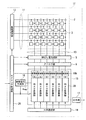
まず、本発明の第1の実施形態を説明する。図1は、本実施形態による(C)MOS撮像装置の構成の一例を示している。図1に示す撮像装置1aは、撮像部2、垂直選択部12、読出し電流源部5、カラム処理部15、参照信号生成部16、変更部18、水平選択部14、出力部17、タイミング制御部20で構成されている。
(First embodiment)
First, a first embodiment of the present invention will be described. FIG. 1 shows an example of the configuration of the (C) MOS imaging device according to the present embodiment. An
撮像部2は、入射される電磁波の大きさに応じた画素信号を生成し出力する単位画素3が複数、行列状に配置されている。垂直選択部12は、撮像部2の各行を選択する。読出し電流源部5は、撮像部2からの信号を電圧信号として読み出す。参照信号生成部16は、時間の経過とともに増加または減少する参照信号Ramp(ランプ波)を生成する。カラム処理部15は参照信号生成部16と接続される。水平選択部14は、AD変換されたデータを水平信号線に読み出す。出力部17は、水平選択部14によって読み出されたデジタルデータを後段の回路に出力する。タイミング制御部20は各部を制御する。
In the
図1では、簡単のため4行×6列の単位画素3から構成される撮像部2の場合について説明しているが、現実には、撮像部2の各行や各列には、数十から数万の単位画素3が配置されることになる。尚、図示を割愛するが、撮像部2を構成する単位画素3は、フォトダイオード/フォトゲート/フォトトランジスタなどの光電変換素子、およびトランジスタ回路によって構成されている。
In FIG. 1, for the sake of simplicity, the case of the
以下では、各部のより詳細な説明を行う。撮像部2は、単位画素3が4行6列分だけ2次元に配置されるとともに、この4行6列の画素配列に対して行ごとに行制御線11が配線されている。行制御線11の各一端は、垂直選択部12の各行に対応した各出力端に接続されている。垂直選択部12は、シフトレジスタあるいはデコーダなどによって構成され、撮像部2の各単位画素3の駆動に際して、行制御線11を介して撮像部2の行アドレスや行走査の制御を行う。また、撮像部2の画素配列に対して列ごとに垂直信号線13が配線されている。読出し電流源部5は、撮像部2からの画素信号を電圧信号として読み出すための電流源で構成されている。
Below, a more detailed description of each part is given. In the
カラム処理部15は、変更部18と、撮像部2の画素列ごと、即ち垂直信号線13ごとに設けられた列AD変換部30とを有する。列AD変換部30.は、比較部31と計測部32を有する。列AD変換部30は、撮像部2の各単位画素3から画素列ごとに垂直信号線13を通して読み出されるアナログの画素信号をデジタルデータに変換する。
The
変更部18はNMOSで構成され、NMOSのソースは、列AD変換部30の比較部31(図2)の第1の入力端に接続され、NMOSのドレインは、所定の電圧を与える電圧源に接続され、ゲートをON(活性化)することでNMOSが短絡される。
The changing
尚、本例では、撮像部2の画素列に対して1対1の対応関係をもって列AD変換部30を配置する構成をとっているが、これは一例に過ぎず、この配置関係に限定されるものではない。例えば、複数の画素列に対して列AD変換部30を1つ配置し、当該1つの列AD変換部30を複数の画素列間で時分割にて使用する構成をとることも可能である。カラム処理部15は、後述する参照信号生成部16と共に、撮像部2の選択画素行の単位画素3から読み出されるアナログの画素信号をデジタルの画素データに変換するアナログ-デジタル変換回路を構成している。尚、列AD変換部30の詳細については後述する。
In this example, the column
参照信号生成部16は、例えば積分回路によって構成され、タイミング制御部20による制御に従って、時間が経過するにつれてレベルが傾斜状に増加あるいは減少する、いわゆるランプ波を生成し、参照信号線を介して列AD変換部30の比較部31(図2)の第2の入力端に参照信号Rampとして供給する。尚、参照信号生成部16としては、積分回路を用いたものに限られるものではなく、DAC回路を用いても構わない。ただし、DAC回路を用いてデジタル的にランプ波を生成する構成をとる場合には、ランプ波のステップを細かくする、あるいはそれと同等な構成をとる必要がある。
The reference
水平選択部14は、シフトレジスタあるいはデコーダなどによって構成され、カラム処理部15の列AD変換部30の列アドレスや列走査の制御を行う。この水平選択部14による制御に従って、列AD変換部30でAD変換されたデジタルデータは順に水平信号線を介して出力部17に読み出される。
The
タイミング制御部20は、垂直選択部12、読出し電流源部5、参照信号生成部16、カラム処理部15、水平選択部14、出力部17などの各部の動作に必要なクロックや所定タイミングのパルス信号を供給するTG(=Timing Generator:タイミングジェネレータ)の機能ブロックと、このTGと通信を行うための機能ブロックとを備える。
The
出力部17は、バッファリング機能以外に、例えば黒レベル調整、列バラツキ補正、色処理などの信号処理機能を内蔵しても構わない。更に、nビットパラレルのデジタルデータをシリアルデータに変換して出力するようにしても構わない。
In addition to the buffering function, the
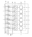
次に、列AD変換部30の構成について説明する。図2は、列AD変換部30を含むカラム処理部15の構成の一例を示している。列AD変換部30は列ごとに設けられており、図1および図2では6個の列AD変換部30が設けられている。各々の列AD変換部30は同一の構成となっている。列AD変換部30は、撮像部2の各単位画素3から垂直信号線13を通して読み出されるアナログの画素信号を、参照信号生成部16から与えられる参照信号Rampと比較することにより、リセットレベルや信号レベルの各々の大きさに対応した時間軸方向の大きさ(パルス幅)を持つパルス信号を生成する。そして、このパルス信号のパルス幅の期間に対応したデータを画素信号の大きさに応じたデジタルデータとすることによってAD変換を行う。
Next, the configuration of the column
以下では、列AD変換部30の構成の詳細について説明する。列AD変換部30は、比較部31および計測部32を備える。
Hereinafter, details of the configuration of the column
比較部31は、第1の入力端に与えられる、撮像部2の単位画素3から垂直信号線13を通して出力されるアナログの画素信号に応じた信号電圧と、第2の入力端に与えられる、参照信号生成部16から供給される参照信号Rampとを比較することによって、画素信号の大きさを時間軸方向の情報(パルス信号のパルス幅)に変換する。比較部31の比較出力は、例えば参照信号Rampのランプ電圧が信号電圧よりも大なるときにはHighレベル(Hレベル)になり、ランプ電圧が信号電圧以下のときにはLowレベル(Lレベル)になる。
The
計測部32は、比較部31による比較開始から比較終了までの比較時間を計測するための、例えばnビットのアップ/ダウンカウンタ回路で構成される。nビットは例えば10ビットである。尚、nビットが10ビットであるのは一例であって、nビットが10ビット未満のビット数(例えば、8ビット)や10ビットを超えるビット数(例えば、12ビット)などであっても構わない。
The measuring
次に、本例の動作について説明する。ここでは、単位画素3の具体的な動作については説明を省略するが、周知のように単位画素3ではリセットレベルと信号レベルとが出力される。
Next, the operation of this example will be described. Here, a description of a specific operation of the
AD変換は、以下のようにして行われる。例えば所定の傾きで下降するランプ波(参照信号Ramp)と、単位画素3からの画素信号であるリセットレベルあるいは信号レベルの各電圧とを比較し、この比較処理で用いるランプ波が生成された時点から、リセットレベルや信号レベルに応じた信号とランプ波(ランプ電圧)とが一致するまでの期間を、例えば基準クロックで計測することによって、リセットレベルあるいは信号レベルの各大きさに対応したデジタルデータを得る。
AD conversion is performed as follows. For example, a ramp wave (reference signal Ramp) that falls at a predetermined slope is compared with a reset level or signal level voltage that is a pixel signal from the
ここで、撮像部2の選択行の各単位画素3からは、アナログの画素信号として、1回目の読出し動作で画素信号の雑音を含むリセットレベルが読み出され、その後、2回目の読出し動作で信号レベルが読み出される。そして、リセットレベルと信号レベルとが垂直信号線13を通して列AD変換部30に時系列で入力される。
Here, from each
<1回目の読出し>
任意の画素行の単位画素3から垂直信号線13への1回目の読出しが安定した後、比較部31のリセット動作が行われる。続いて、変更部18は、リセットレベルが与えられた比較部31の第1の入力端の電圧を、リセットレベルよりも低い所定の電圧に変更する。その後、タイミング制御部20は、参照信号生成部16に対して、ランプ波生成の制御データを供給する。これを受けて参照信号生成部16は、比較部31の第2の入力端に与える比較電圧として、波形が全体として時間的にランプ状に変化するランプ波(参照信号Ramp)を出力する。比較部31は、参照信号生成部16からのランプ波が与えられた第2の入力端の電圧と、リセットレベルが与えられた第1の入力端の電圧とを比較し、双方の電圧が略一致したときに、比較出力を反転させる。
<First reading>
After the first reading from the
計測部32は、比較部31での比較開始に基づいてダウンカウントモードで計測を開始し、比較部31の比較出力が反転した時点の計測値を保持する。つまり、計測部32は、リセットレベルに応じたデジタルデータを保持する。タイミング制御部20は、所定の期間を経過すると、参照信号生成部16への制御データの供給と、基準クロックの出力とを停止する。これにより、参照信号生成部16は、ランプ波の生成を停止する。
The
<2回目の読出し>
続いて、2回目の読出し時には、単位画素3毎の入射光量に応じた信号レベルが読み出される。この2回目の読出し時には、比較部31のリセット動作および変更部18による変更動作は行わない。
<Second reading>
Subsequently, in the second reading, a signal level corresponding to the incident light amount for each
任意の画素行の単位画素3から垂直信号線13への2回目の読出しが安定した後、タイミング制御部20は、参照信号生成部16に対して、ランプ波生成の制御データを供給する。これを受けて参照信号生成部16はランプ波(参照信号Ramp)を出力する。比較部31は、参照信号生成部16からのランプ波が与えられた第2の入力端の電圧と、信号レベルが与えられた第1の入力端の電圧とを比較し、双方の電圧が略一致したときに、比較出力を反転させる。
After the second reading from the
計測部32は、比較部31での比較開始に基づいてアップカウントモードで計測を開始し、比較部31の比較出力が反転した時点の計測値を保持する。つまり、計測部32は、信号レベルからリセットレベルを減算(CDS(=Correlated Double Sampling:相関2重サンプリング)処理)した信号成分に応じたデジタルデータを保持する。タイミング制御部20は、所定の期間を経過すると、参照信号生成部16への制御データの供給と、基準クロックの出力とを停止する。これにより、参照信号生成部16は、ランプ波の生成を停止する。
The
次に、比較部31と変更部18の構成および比較部31の入力端における電圧変化の詳細を説明する。図3は、比較部31および変更部18の具体的な回路構成の一例である。以下、本例の回路構成について説明する。
Next, the configuration of the
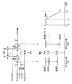
図3において、比較部31内の差動アンプは、ソースが共通に接続されたNMOSで構成されるトランジスタN1,N2と、これらトランジスタN1,N2の各ドレインと電源VDDとの間に接続され、ゲートが共通に接続されたPMOSで構成されるトランジスタP3,P4と、トランジスタN1,N2のソースに共通に接続されたノードとグランドGNDとの間に接続されたNMOSの電流源N5とから構成されている。
In FIG. 3, the differential amplifier in the
この差動アンプにおいて、トランジスタN1,N2の各ゲートとドレインとの間に、PMOSで構成されるトランジスタP6,P7がそれぞれ接続されている。これらトランジスタP6,P7は、各ゲートにLowアクティブのリセットパルスResetがタイミング制御部20から与えられることでON状態となり、トランジスタN1,N2の各ゲートとドレインとを短絡し、トランジスタN1,N2の各ゲートの電圧、即ち差動アンプの2つの入力端IN1,IN2の電圧をリセットするリセット部として機能する。
In this differential amplifier, transistors P6 and P7 made of PMOS are connected between the gates and drains of the transistors N1 and N2, respectively. These transistors P6 and P7 are turned on when a low active reset pulse Reset is given to each gate from the
トランジスタN1,N2の各ゲートには、DCレベルをカットするための容量素子C1,C2の各一端がそれぞれ接続されている。容量素子C1の他端には、撮像部2の各単位画素3から出力される画素信号Pixelが与えられる。容量素子C2の他端には、参照信号生成部16からの参照信号Rampが与えられる。
One end of each of capacitive elements C1 and C2 for cutting the DC level is connected to each gate of the transistors N1 and N2. A pixel signal Pixel output from each
全列で共通のスイッチ素子SW1(第1のスイッチ素子)は変更部18を構成する。スイッチ素子SW1の一端はトランジスタN1のゲートに接続され、スイッチ素子SW1の他端は、例えば電圧源VDDLに接続される。電圧源VDDLが供給する電圧VDDLは、リセットレベルよりも低い電圧となるように予め調整されている。スイッチ素子SW1は、例えばNMOSで構成され、タイミング制御部20からの図示しない制御信号によってON状態とOFF状態が制御される。また、電流源N5のゲートには、電流値を制御するためのバイアス電圧Vbiasが与えられる。
The switch element SW1 (first switch element) that is common to all the columns constitutes the changing
以下、本例の動作について説明する。ここでは、リセットレベルの電圧をVR、信号レベルの電圧をVS(ただし、VS≦VR)、電圧源VDDLの電圧をVDDLとする。図3には、比較部31内の差動アンプの第1の入力端IN1および第2の入力端IN2の電圧変化および参照信号Rampの波形が示されている。
The operation of this example will be described below. Here, the reset level voltage is V R , the signal level voltage is V S (where V S ≦ V R ), and the voltage of the voltage source VDDL is V DDL . FIG. 3 shows the voltage change of the first input terminal IN1 and the second input terminal IN2 of the differential amplifier in the
単位画素3からの画素信号Pixelとしてリセットレベルが第1の入力端IN1に与えられ、参照信号生成部16から第2の入力端IN2に与えられる参照信号Rampが安定した後、タイミング制御部20が比較部31の比較開始前にリセットパルスResetを活性化(Lowアクティブ)する。これにより、トランジスタP6,P7がON状態となってトランジスタN1,N2の各ゲートとドレインとを短絡し、これらトランジスタN1,N2の動作点をドレイン電圧として2つの入力端の電圧がリセットされる。
After the reset level is given to the first input terminal IN1 as the pixel signal Pixel from the
このリセットによって決定された動作点で、差動アンプの2つの入力端の電圧、即ちトランジスタN1,N2の各ゲート電圧のオフセット成分がほぼキャンセルされる。即ち、差動アンプの2つの入力端の電圧が、略同一の電圧VRSTになるようにリセットされる。この時点(時刻T1)で、第1の入力端IN1の電圧はVRST、第2の入力端IN2の電圧はVRSTである。リセット後、トランジスタP6,P7はOFF状態となる。 At the operating point determined by this reset, the voltages at the two input terminals of the differential amplifier, that is, the offset components of the gate voltages of the transistors N1 and N2, are almost canceled. That is, the voltages at the two input terminals of the differential amplifier are reset so as to be substantially the same voltage VRST . At this time (time T1), the voltage at the first input terminal IN1 is V RST and the voltage at the second input terminal IN2 is V RST . After reset, the transistors P6 and P7 are turned off.
続いて、スイッチ素子SW1がOFF状態からON状態となることで、画素信号Pixelが与えられる第1の入力端IN1の電圧、即ちトランジスタN1のゲート電圧が電圧VRSTから所定の電圧VDDL(VDDL<VRST)に低く変更される。この時点(時刻T2)で、第1の入力端IN1の電圧はVDDL、第2の入力端IN2の電圧はVRSTである。スイッチ素子SW1はON状態となった後、OFF状態となる。 Subsequently, when the switch element SW1 is changed from the OFF state to the ON state, the voltage of the first input terminal IN1 to which the pixel signal Pixel is applied, that is, the gate voltage of the transistor N1 is changed from the voltage V RST to the predetermined voltage V DDL (V DDL <V RST ). At this time (time T2), the voltage at the first input terminal IN1 is V DDL , and the voltage at the second input terminal IN2 is V RST . The switch element SW1 is turned on after being turned on.
VDDL<VRSTであるため、1回目の読出しに係る比較部31での比較開始時の第1の入力端IN1の電圧は、参照信号Rampが与えられる第2の入力端IN2の電圧よりも低くなる。つまり、比較部31のリセット動作後に、比較部31を構成する差動アンプの2つの入力端の電圧に多少のばらつきが残ったとしても、変更部18により、リセットレベルが与えられた比較部31の第1の入力端の電圧をより低い電圧に変更することで、ランプ波が与えられる第2の入力端の電圧が、リセットレベルが与えられた第1の入力端の電圧よりも高くなる。図3に示すように、参照信号Rampとして時間の経過とともに減少するランプ波を与えることで、比較部31の出力を比較動作中に確実に反転させ、比較部31による比較動作を保証することができる。
Since V DDL <V RST , the voltage of the first input terminal IN1 at the start of comparison in the
時刻T2以降、第2の入力端に参照信号Rampとしてランプ波が与えられる。ランプ波が与えられた第2の入力端の電圧と、リセットされた第1の入力端の電圧とが略一致したタイミングで比較部31の比較出力が反転する。第2の入力端へのランプ波の入力が開始されてから所定の期間が経過した時点(時刻T3)で、参照信号生成部16はランプ波の生成を停止する。
After time T2, a ramp wave is given as a reference signal Ramp to the second input terminal. The comparison output of the
続いて、単位画素3からの画素信号Pixelとして信号レベルが第1の入力端IN1に与えられる。以下では、図4を用いて、信号レベルが入力された時点(時刻T4)での第1の入力端IN1の電圧を説明する。図4は、第1の入力端の周辺の構成のみを抽出して示している。以下では、第1の入力端IN1とグランドGNDとの間の寄生容量CPを仮定して説明を行う。
Subsequently, a signal level is given to the first input terminal IN1 as a pixel signal Pixel from the
スイッチ素子SW1によって第1の入力端IN1の電圧がVRSTからVDDLに変更された時点(時刻T2)で、画素信号Pixelとしてリセットレベルが与えられている容量素子C1の他端の電圧はVRである。また、画素信号Pixelとして信号レベルが入力された時点(時刻T4)で、容量素子C1の他端の電圧はVSとなる。時刻T2から時刻T4までの容量素子C1の他端の電圧の変化をΔV1とすると、ΔV1は以下の(1)式となる。
ΔV1 = VS - VR ・・・(1)
When the voltage of the first input terminal IN1 is changed from V RST to V DDL by the switch element SW1 (time T2), the voltage at the other end of the capacitive element C1 to which the reset level is given as the pixel signal Pixel is V R. At the time (time T4) when the signal level is input as the pixel signal Pixel, the voltage at the other end of the capacitive element C1 becomes V S. Assuming that the change in voltage at the other end of the capacitive element C1 from time T2 to time T4 is ΔV1, ΔV1 is expressed by the following equation (1).
ΔV1 = V S -V R (1)
時刻T2から時刻T4までの間、トランジスタP6およびスイッチ素子SW1はOFF状態であるため、容量素子C1および寄生容量CPに蓄積されている電荷量は保持される。このため、時刻T2から時刻T4までの第1の入力端IN1の電圧の変化をΔV2とすると、ΔV2は以下の(2)式となる。尚、(2)式において、C1は容量素子C1の容量値、CPは寄生容量CPの容量値である。 Since the transistor P6 and the switch element SW1 are in the OFF state from time T2 to time T4, the charge amount accumulated in the capacitive element C1 and the parasitic capacitance CP is held. Therefore, if the change in voltage at the first input terminal IN1 from time T2 to time T4 is ΔV2, ΔV2 is expressed by the following equation (2). In equation (2), C 1 is the capacitance value of the capacitive element C 1 , and C P is the capacitance value of the parasitic capacitance CP.

C1に比べてCPを無視できる場合(C1>> CP)、ΔV2=ΔV1となる。時刻T2における第1の入力端IN1の電圧はVDDLであるので、(1)式を用いて、時刻T4における第1の入力端IN1の電圧VIN1は以下の(3)式となる。
VIN1 = VDDL +(VS - VR) ・・・(3)
If you can ignore the C P compared to C 1 (C 1 >> C P ), the ΔV2 = ΔV1. Since the voltage at the first input terminal IN1 at the time T2 is V DDL , the voltage VIN1 at the first input terminal IN1 at the time T4 is expressed by the following expression (3) using the expression (1).
VIN1 = V DDL + (V S -V R ) (3)
前述したようにVDDL<VRSTであり、更にVS≦VRであるため、2回目の読出しに係る比較部31での比較開始時の第1の入力端IN1の電圧は、参照信号Rampが与えられる第2の入力端IN2の電圧よりも低くなる。図3に示すように、参照信号Rampとして時間の経過とともに減少するランプ波が与えられるので、比較部31の出力を比較動作中に確実に反転させ、比較部31による比較動作を保証することができる。
As described above, since V DDL <V RST and V S ≦ V R , the voltage of the first input terminal IN1 at the start of comparison in the
時刻T4以降、第2の入力端に参照信号Rampとしてランプ波が与えられる。ランプ波が与えられた第2の入力端の電圧と、第1の入力端の電圧とが略一致したタイミングで比較部31の比較出力が反転する。第2の入力端へのランプ波の入力が開始されてから所定の期間が経過した時点(時刻T5)で、参照信号生成部16はランプ波の生成を停止する。1回目の読出し時に計測部32がダウンカウントモードで計測を行い、2回目の読出し時に計測部32がアップカウントモードで計測を行うため、計測部32の計測値として、(3)式の右辺第2項に相当する信号成分(VS - VR)に係る計測値が得られる。
After time T4, a ramp wave is given to the second input terminal as the reference signal Ramp. The comparison output of the
上述したように、本実施形態によれば、トランジスタP6,P7によるリセット動作後に、第1の入力端IN1と第2の入力端IN2との電圧差が、比較部31による比較動作を保証する電圧となるように、変更部18(スイッチ素子SW1)が第1の入力端IN1の電圧をより低い電圧に変更することによって、比較部31が参照信号Rampと画素信号Pixelとの比較動作を確実に行うことができる。更に、スイッチ素子SW1で変更部18を構成することによって、容易な構成で電圧の変更を行うことができる。
As described above, according to this embodiment, after the reset operation by the transistors P6 and P7, the voltage difference between the first input terminal IN1 and the second input terminal IN2 guarantees the comparison operation by the
また、参照信号Rampが与えられる第2の入力端IN2の電圧をより高い電圧に変更するのではなく、画素信号Pixelが与えられる第1の入力端IN1の電圧をより低い電圧に変更することによって、前述した第1の問題および第3の問題を解決することができる。 Further, instead of changing the voltage at the second input terminal IN2 to which the reference signal Ramp is applied to a higher voltage, the voltage at the first input terminal IN1 to which the pixel signal Pixel is applied is changed to a lower voltage. The first problem and the third problem described above can be solved.
(第2の実施形態)
次に、本発明の第2の実施形態を説明する。本実施形態の(C)MOS撮像装置の構成は、第1の実施形態で説明した構成と略同様(図1)であり、AD変換動作のみが異なる。
(Second Embodiment)
Next, a second embodiment of the present invention will be described. The configuration of the (C) MOS imaging device of this embodiment is substantially the same as the configuration described in the first embodiment (FIG. 1), and only the AD conversion operation is different.
以下では、本例の動作のうち、第1の実施形態と異なる部分を中心に説明する。第1の実施形態と同様に、単位画素3ではリセットレベルと信号レベルとが出力される。
Below, it demonstrates centering on a different part from 1st Embodiment among operation | movement of this example. As in the first embodiment, the
AD変換は、以下のようにして行われる。例えば所定の傾きで下降するランプ波(参照信号Ramp)と、単位画素3からの画素信号であるリセットレベルおよび信号レベルの差分に応じた電圧(差分信号レベル)とを比較し、この比較処理で用いるランプ波が生成された時点から、差分信号レベルに応じた信号とランプ波(ランプ電圧)とが一致するまでの期間を、例えば基準クロックで計測することによって、差分信号レベルの大きさに対応したデジタルデータを得る。
AD conversion is performed as follows. For example, a ramp wave (reference signal Ramp) that falls at a predetermined slope is compared with a voltage (difference signal level) corresponding to a difference between a reset level and a signal level that is a pixel signal from the
ここで、撮像部2の選択行の各単位画素3からは、アナログの画素信号として、1回目の読出し動作でリセットレベルが読み出され、その後、2回目の読出し動作で信号レベルが読み出される。そして、リセットレベルと信号レベルとが垂直信号線13を通して列AD変換部30に時系列で入力される。
Here, from each
<1回目の読出し>
任意の画素行の単位画素3から垂直信号線13への1回目の読出しが安定した後、比較部31のリセット動作が行われる。続いて、変更部18は、リセットレベルが与えられた比較部31の第1の入力端の電圧を、リセットレベルよりも低い所定の電圧に変更する。
<First reading>
After the first reading from the
<2回目の読出し>
続いて、2回目の読出し時には、単位画素3毎の入射光量に応じた信号レベルが読み出される。この2回目の読出し時には、比較部31のリセット動作および変更部18による変更動作は行わない。
<Second reading>
Subsequently, in the second reading, a signal level corresponding to the incident light amount for each
任意の画素行の単位画素3から垂直信号線13への2回目の読出しが安定した後、タイミング制御部20は、参照信号生成部16に対して、ランプ波生成の制御データを供給する。これを受けて参照信号生成部16はランプ波(参照信号Ramp)を出力する。比較部31は、参照信号生成部16からのランプ波が与えられた第2の入力端の電圧と、差分信号レベルが与えられた第1の入力端の電圧とを比較し、双方の電圧が略一致したときに、比較出力を反転させる。
After the second reading from the
計測部32は、比較部31での比較開始に基づいてアップカウントモードで計測を開始し、比較部31の比較出力が反転した時点の計測値を保持する。つまり、計測部32は、信号レベルからリセットレベルを減算(CDS処理)した信号成分に応じたデジタルデータを保持する。タイミング制御部20は、所定の期間を経過すると、参照信号生成部16への制御データの供給と、基準クロックの出力とを停止する。これにより、参照信号生成部16は、ランプ波の生成を停止する。
The
次に、比較部31の入力端における電圧変化の詳細を説明する。図5は、比較部31および変更部18の具体的な回路構成の一例である。図5に示す回路構成は、図3に示した回路構成と略同様であるので説明を省略する。
Next, details of the voltage change at the input terminal of the
以下、本例の動作について説明する。ここでは、リセットレベルの電圧をVR、信号レベルの電圧をVS(ただし、VS≦VR)、電圧源VDDLの電圧をVDDLとする。図5には、比較部31内の差動アンプの第1の入力端IN1および第2の入力端IN2の電圧変化および参照信号Rampの波形が示されている。
The operation of this example will be described below. Here, the reset level voltage is V R , the signal level voltage is V S (where V S ≦ V R ), and the voltage of the voltage source VDDL is V DDL . FIG. 5 shows the voltage change of the first input terminal IN1 and the second input terminal IN2 of the differential amplifier in the
単位画素3からの画素信号Pixelとしてリセットレベルが第1の入力端IN1に与えられ、参照信号生成部16から第2の入力端IN2に与えられる参照信号Rampが安定した後、2つの入力端の電圧がリセットされる。このとき、差動アンプの2つの入力端の電圧が、略同一の電圧VRSTになるようにリセットされる。この時点(時刻T1)で、第1の入力端IN1の電圧はVRST、第2の入力端IN2の電圧はVRSTである。リセット後、トランジスタP6,P7はOFF状態となる。
After the reset level is given to the first input terminal IN1 as the pixel signal Pixel from the
続いて、スイッチ素子SW1がOFF状態からON状態となることで、画素信号Pixelが与えられる第1の入力端IN1の電圧、即ちトランジスタN1のゲート電圧が電圧VRSTから所定の電圧VDDL(VDDL<VRST)に低く変更される。この時点(時刻T2)で、第1の入力端IN1の電圧はVDDL、第2の入力端IN2の電圧はVRSTである。スイッチ素子SW1はON状態となった後、OFF状態となる。 Subsequently, when the switch element SW1 is changed from the OFF state to the ON state, the voltage of the first input terminal IN1 to which the pixel signal Pixel is applied, that is, the gate voltage of the transistor N1 is changed from the voltage V RST to the predetermined voltage V DDL (V DDL <V RST ). At this time (time T2), the voltage at the first input terminal IN1 is V DDL , and the voltage at the second input terminal IN2 is V RST . The switch element SW1 is turned on after being turned on.
続いて、単位画素3からの画素信号Pixelとして信号レベルが第1の入力端IN1に与えられる。信号レベルが入力された時点(時刻T4)での第1の入力端IN1の電圧VIN1は、第1の実施形態と同様に以下の(4)式となる。
VIN1 = VDDL +(VS - VR) ・・・(4)
Subsequently, a signal level is given to the first input terminal IN1 as a pixel signal Pixel from the
VIN1 = V DDL + (V S -V R ) (4)
前述したようにVDDL<VRSTであり、更にVS≦VRであるため、比較部31での比較開始時の第1の入力端IN1の電圧は、参照信号Rampが与えられる第2の入力端IN2の電圧よりも低くなる。参照信号Rampとして時間の経過とともに減少するランプ波が与えられるので、比較部31の出力を比較動作中に確実に反転させ、比較部31による比較動作を保証することができる。
As described above, since V DDL <V RST and V S ≦ V R , the voltage at the first input terminal IN1 at the start of comparison in the
時刻T4以降、第2の入力端に参照信号Rampとしてランプ波が与えられる。ランプ波が与えられた第2の入力端の電圧と、第1の入力端の電圧とが略一致したタイミングで比較部31の比較出力が反転する。第2の入力端へのランプ波の入力が開始されてから所定の期間が経過した時点(時刻T5)で、参照信号生成部16はランプ波の生成を停止する。2回目の読出し時に計測部32がアップカウントモードで計測を行うため、計測部32の計測値として、(4)式のVDDL +(VS - VR)に係る計測値が得られる。
After time T4, a ramp wave is given to the second input terminal as the reference signal Ramp. The comparison output of the
本実施形態では、1回のAD変換動作でデジタルデータを得ることが可能となる。尚、リセットレベルが与えられた第1の入力端を所定の電圧に低く変更することで信号成分(VS - VR)にオフセット成分(VDDL)が重畳したデジタルデータが得られるが、撮像部2に設けられた遮光画素やダミー画素のデータを用いてオフセット成分のデジタルデータを演算し、計測部32の計測値からオフセット成分のデジタルデータを減算することで、オフセット成分を抑圧することが可能である。
In the present embodiment, digital data can be obtained by a single AD conversion operation. Note that digital data in which the offset component (V DDL ) is superimposed on the signal component (V S −V R ) can be obtained by changing the first input terminal to which the reset level is given to a predetermined voltage. It is possible to suppress the offset component by calculating the digital data of the offset component using the data of the shading pixel and the dummy pixel provided in the
また、参照信号Rampが与えられる第2の入力端IN2の電圧をより高い電圧に変更するのではなく、画素信号Pixelが与えられる第1の入力端IN1の電圧をより低い電圧に変更することによって、前述した第1の問題および第3の問題を解決することができる。 Further, instead of changing the voltage at the second input terminal IN2 to which the reference signal Ramp is applied to a higher voltage, the voltage at the first input terminal IN1 to which the pixel signal Pixel is applied is changed to a lower voltage. The first problem and the third problem described above can be solved.
(第3の実施形態)
次に、本発明の第3の実施形態を説明する。図6は、本実施形態による(C)MOS撮像装置の構成の一例を示している。以下、本例の構成について説明する。図6に示す撮像装置1bの構成のうち、図1と異なるのはアナログ部6の構成である。本例のアナログ部6は、減算(CDS処理)回路を有する。アナログ部6以外の構成は、図1に示した構成と略同様であるので説明は省略する。
(Third embodiment)
Next, a third embodiment of the present invention will be described. FIG. 6 shows an example of the configuration of the (C) MOS imaging device according to the present embodiment. Hereinafter, the configuration of this example will be described. Of the configuration of the
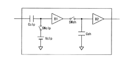
図7は、アナログ部6の構成の一例を示している。図7に示す構成は、第1の信号電圧と第2の信号電圧との差分に応じた信号成分を取得する手段として、CDS処理機能を備えるようにした構成である。アナログ部6は、垂直信号線13に接続されたクランプ容量Cclp、クランプ容量CclpをクランプバイアスVclpにクランプするためのクランプスイッチSWclp、信号をサンプルホールドするためのサンプルホールド容量Csh、サンプルホールドスイッチSWsh、バッファ部B1、およびバッファ部B2で構成されている。CDS処理を行う場合、アナログ部6は、タイミング制御部20から与えられるクランプパルスとサンプリングパルスとの2つのパルスに基づいて、クランプスイッチSWclpおよびサンプルホールドスイッチSWshを制御し、垂直信号線13を介して入力された電圧モードの画素信号に対して、リセットレベルと信号レベルとの減算(CDS処理)を行うことで、信号成分を取得する。
FIG. 7 shows an example of the configuration of the
次に、本例の動作について説明する。第1の実施形態による撮像装置1aの動作と異なるのは、アナログ部6に減算(CDS処理)回路を設けたことによるAD変換動作である。以下では、本例の動作のうち、第1の実施形態と異なる部分を中心に説明する。第1の実施形態と同様に、単位画素3ではリセットレベルと信号レベルとが出力される。ここでは、リセットレベルの電圧をVR、信号レベルの電圧をVS(ただし、VS≦VR)とする。
Next, the operation of this example will be described. What is different from the operation of the
AD変換は、以下のようにして行われる。例えば所定の傾きで下降するランプ波(参照信号Ramp)と、単位画素3からの画素信号であるリセットレベルおよび信号レベルの差分に応じた電圧(差分信号レベル)とを比較し、この比較処理で用いるランプ波が生成された時点から、差分信号レベルに応じた信号とランプ波(ランプ電圧)とが一致するまでの期間を、例えば基準クロックで計測することによって、差分信号レベルの大きさに対応したデジタルデータを得る。
AD conversion is performed as follows. For example, a ramp wave (reference signal Ramp) that falls at a predetermined slope is compared with a voltage (difference signal level) corresponding to a difference between a reset level and a signal level that is a pixel signal from the
ここで、撮像部2の選択行の各単位画素3からは、アナログの画素信号として、1回目の読出し動作でリセットレベルが読み出され、その後、2回目の読出し動作で信号レベルが読み出される。そして、リセットレベルと信号レベルとが垂直信号線13を通してアナログ部6に時系列で入力される。
Here, from each
<1回目の読出し>
任意の画素行の単位画素3から垂直信号線13への1回目の読出しが安定した後、クランプスイッチSWclpおよびサンプルホールドスイッチSWshがON状態となり、更に比較部31のリセット動作が行われる。続いて、変更部18は、リセットレベルが与えられた比較部31の第1の入力端の電圧を、リセットレベルよりも低い所定の電圧に変更する。続いて、クランプスイッチSWclpがOFF状態となる。
<First reading>
After the first reading from the
<2回目の読出し>
続いて、2回目の読出し時には、単位画素3毎の入射光量に応じた信号レベルが読み出される。この2回目の読出し時には、比較部31のリセット動作および変更部18による変更動作は行わない。また、クランプスイッチSWclpがOFF状態であるため、クランプ容量Cclpに入力される電圧がリセットレベルから信号レベルに変化すると、バッファ部B1の入力電圧が、その変化に応じた電圧(VS - VR)だけ変化する。この変化に応じて、バッファ部B2の入力電圧および出力電圧も同様に変化する。これによって、比較部31の第1の入力端には、信号レベルとリセットレベルとの差分信号レベル(VS - VR)が与えられる。信号レベルの読出し後、サンプルホールドスイッチSWshがOFF状態となる。
<Second reading>
Subsequently, in the second reading, a signal level corresponding to the incident light amount for each
任意の画素行の単位画素3から垂直信号線13への2回目の読出しが安定した後、タイミング制御部20は、参照信号生成部16に対して、ランプ波生成の制御データを供給する。これを受けて参照信号生成部16はランプ波(参照信号Ramp)を出力する。比較部31は、このランプ波が与えられた第2の入力端の電圧と、差分信号レベルが与えられた第1の入力端の電圧とを比較する。
After the second reading from the
本実施形態では、第1の実施形態と同様に、比較部31のリセット動作後に、比較部31を構成する差動アンプの2つの入力端の電圧に多少のばらつきが残ったとしても、比較部31での比較開始時の第1の入力端IN1の電圧は、参照信号Rampが与えられる第2の入力端IN2の電圧よりも低くなる。このため、比較部31の出力を比較動作中に確実に反転させ、比較部31による比較動作を保証することができる。
In the present embodiment, as in the first embodiment, after the reset operation of the
比較部31は、参照信号生成部16からのランプ波が与えられた第2の入力端の電圧と、差分信号レベルが与えられた第1の入力端の電圧とを比較し、双方の電圧が略一致したときに、比較出力を反転させる。計測部32は、比較部31での比較開始に基づいてアップカウントモードで計測を開始し、比較部31の比較出力が反転した時点の計測値を保持する。つまり、計測部32は、信号レベルからリセットレベルを減算(CDS処理)した信号成分に応じたデジタルデータを保持する。タイミング制御部20は、所定の期間を経過すると、参照信号生成部16への制御データの供給と、基準クロックの出力とを停止する。これにより、参照信号生成部16は、ランプ波の生成を停止する。2回目の読出し時に計測部32がアップカウントモードで計測を行うため、計測部32の計測値として、(3)式のVDDL +(VS - VR)に係る計測値が得られる。
The
本実施形態では、1回のAD変換動作でデジタルデータを得ることが可能となる。尚、リセットレベルが与えられた第1の入力端を所定の電圧に低く変更することで信号成分(VS - VR)にオフセット成分(VDDL)が重畳したデジタルデータが得られるが、撮像部2に設けられた遮光画素やダミー画素のデータを用いてオフセット成分のデジタルデータを演算し、計測部32の計測値からオフセット成分のデジタルデータを減算することで、オフセット成分を抑圧することが可能である。
In the present embodiment, digital data can be obtained by a single AD conversion operation. Note that digital data in which the offset component (V DDL ) is superimposed on the signal component (V S −V R ) can be obtained by changing the first input terminal to which the reset level is given to a predetermined voltage. It is possible to suppress the offset component by calculating the digital data of the offset component using the data of the shading pixel and the dummy pixel provided in the
また、参照信号Rampが与えられる第2の入力端IN2の電圧をより高い電圧に変更するのではなく、画素信号Pixelが与えられる第1の入力端IN1の電圧をより低い電圧に変更することによって、前述した第1の問題および第3の問題を解決することができる。 Further, instead of changing the voltage at the second input terminal IN2 to which the reference signal Ramp is applied to a higher voltage, the voltage at the first input terminal IN1 to which the pixel signal Pixel is applied is changed to a lower voltage. The first problem and the third problem described above can be solved.
(第4の実施形態)
次に、本発明の第4の実施形態を説明する。図8は、本実施形態による(C)MOS撮像装置の構成の一例を示している。以下、本例の構成について説明する。図8に示す撮像装置1cの構成のうち、図1と異なるのは変更部18aの構成である。本例の変更部18aは、列毎に設けられており、容量素子およびスイッチ素子で構成される。変更部18a以外の構成は、図1に示した構成と略同様であるので説明は省略する。
(Fourth embodiment)
Next, a fourth embodiment of the present invention will be described. FIG. 8 shows an example of the configuration of the (C) MOS imaging device according to the present embodiment. Hereinafter, the configuration of this example will be described. Of the configuration of the
以下では、本例の動作のうち、第1の実施形態と異なる部分を中心に説明する。第1の実施形態と同様に、単位画素3ではリセットレベルと信号レベルとが出力される。
Below, it demonstrates centering on a different part from 1st Embodiment among operation | movement of this example. As in the first embodiment, the
AD変換は、以下のようにして行われる。例えば所定の傾きで下降するランプ波(参照信号Ramp)と、単位画素3からの画素信号であるリセットレベルあるいは信号レベルの各電圧とを比較し、この比較処理で用いるランプ波が生成された時点から、リセットレベルや信号レベルに応じた信号とランプ波(ランプ電圧)とが一致するまでの期間を、例えば基準クロックで計測することによって、リセットレベルあるいは信号レベルの各大きさに対応したデジタルデータを得る。
AD conversion is performed as follows. For example, a ramp wave (reference signal Ramp) that falls at a predetermined slope is compared with a reset level or signal level voltage that is a pixel signal from the
ここで、撮像部2の選択行の各単位画素3からは、アナログの画素信号として、1回目の読出し動作でリセットレベルが読み出され、その後、2回目の読出し動作で信号レベルが読み出される。そして、リセットレベルと信号レベルとが垂直信号線13を通して列AD変換部30に時系列で入力される。
Here, from each
<1回目の読出し>
任意の画素行の単位画素3から垂直信号線13への1回目の読出しが安定した後、比較部31のリセット動作が行われる。続いて、変更部18aは、リセットレベルが与えられた比較部31の第1の入力端の電圧を、リセットレベルよりも低い所定の電圧に変更する。変更部18aによる変更動作の詳細については、後述する。その後、タイミング制御部20は、参照信号生成部16に対して、ランプ波生成の制御データを供給する。これを受けて参照信号生成部16はランプ波(参照信号Ramp)を出力する。比較部31は、参照信号生成部16からのランプ波が与えられた第2の入力端の電圧と、リセットレベルが与えられた第1の入力端の電圧とを比較し、双方の電圧が略一致したときに、比較出力を反転させる。
<First reading>
After the first reading from the
計測部32は、比較部31での比較開始に基づいてダウンカウントモードで計測を開始し、比較部31の比較出力が反転した時点の計測値を保持する。つまり、計測部32は、リセットレベルに応じたデジタルデータを保持する。タイミング制御部20は、所定の期間を経過すると、参照信号生成部16への制御データの供給と、基準クロックの出力とを停止する。これにより、参照信号生成部16は、ランプ波の生成を停止する。
The
<2回目の読出し>
続いて、2回目の読出し時には、単位画素3毎の入射光量に応じた信号レベルが読み出される。この2回目の読出し時には、比較部31のリセット動作および変更部18aによる変更動作は行わない。
<Second reading>
Subsequently, in the second reading, a signal level corresponding to the incident light amount for each
任意の画素行の単位画素3から垂直信号線13への2回目の読出しが安定した後、タイミング制御部20は、参照信号生成部16に対して、ランプ波生成の制御データを供給する。これを受けて参照信号生成部16はランプ波(参照信号Ramp)を出力する。比較部31は、参照信号生成部16からのランプ波が与えられた第2の入力端の電圧と、信号レベルが与えられた第1の入力端の電圧とを比較し、双方の電圧が略一致したときに、比較出力を反転させる。
After the second reading from the
計測部32は、比較部31での比較開始に基づいてアップカウントモードで計測を開始し、比較部31の比較出力が反転した時点の計測値を保持する。つまり、計測部32は、信号レベルからリセットレベルを減算(CDS処理)した信号成分に応じたデジタルデータを保持する。タイミング制御部20は、所定の期間を経過すると、参照信号生成部16への制御データの供給と、基準クロックの出力とを停止する。これにより、参照信号生成部16は、ランプ波の生成を停止する。
The
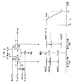
次に、比較部31と変更部18aの構成および比較部31の入力端における電圧変化の詳細を説明する。図9は、比較部31および変更部18aの具体的な回路構成の一例である。図10は、比較部31および変更部18aを含むカラム処理部15の回路構成の一例である。以下、本例の回路構成について説明する。以下では、図3に示した構成と異なる構成についてのみ説明する。
Next, the configuration of the
変更部18aは、列毎に設けられたスイッチ素子SW2(第2のスイッチ素子)および容量素子C3(第2の容量素子)で構成されている。容量素子C3の一端はトランジスタN1のゲートに接続され、容量素子C3の他端はスイッチ素子SW2の第1の端子に接続される。スイッチ素子SW2の第2の端子は電圧源V1(第1の電圧源)に接続され、スイッチ素子SW2の第3の端子は電圧源V2(第2の電圧源)に接続される。スイッチ素子SW2は、第1の端子および第2の端子を短絡して電圧源V1と容量素子C3の他端とが接続された状態と、第1の端子および第3の端子を短絡して電圧源V2と容量素子C3の他端とが接続された状態との切替を行う。
The changing
以下、本例の動作について説明する。ここでは、電圧源V1の電圧をV1、電圧源V2の電圧をV2(ただし、V2<V1)、リセットレベルの電圧をVR(ただし、電源VDDの電圧をVDDとしたとき、VR<VDD)、信号レベルの電圧をVS(ただし、VS≦VR)、容量素子C1の容量値をC1、容量素子C3の容量値をC3とする。図9には、比較部31内の差動アンプの第1の入力端IN1および第2の入力端IN2の電圧変化および参照信号Rampの波形が示されている。
The operation of this example will be described below. Here, the voltage of the voltage source V1 is V 1 , the voltage of the voltage source V2 is V 2 (where V 2 <V 1 ), and the reset level voltage is V R (where the power supply VDD voltage is V DD , V R <V DD ), the signal level voltage is V S (where V S ≦ V R ), the capacitance value of the capacitive element C1 is C 1 , and the capacitive value of the capacitive element C3 is C 3 . FIG. 9 shows the voltage change of the first input terminal IN1 and the second input terminal IN2 of the differential amplifier in the
単位画素3からの画素信号Pixelとしてリセットレベルが第1の入力端IN1に与えられ、参照信号生成部16から第2の入力端IN2に与えられる参照信号Rampが安定した後、2つの入力端の電圧がリセットされる。このとき、差動アンプの2つの入力端の電圧が、略同一の電圧VRSTになるようにリセットされる。この時点(時刻T1)で、第1の入力端IN1の電圧はVRST、第2の入力端IN2の電圧はVRSTである。リセット動作中、容量素子C3の他端は、スイッチ素子SW2により電圧源V1に接続されている。リセット後、トランジスタP6,P7はOFF状態となる。
After the reset level is given to the first input terminal IN1 as the pixel signal Pixel from the
続いて、スイッチ素子SW2が容量素子C3の他端を電圧源V2に接続することで、画素信号Pixelが与えられる第1の入力端IN1の電圧、即ちトランジスタN1のゲート電圧が電圧VRSTから所定の電圧に低く変更される。容量素子C3の他端の電圧がV1からV2に(V2 - V1)だけ変化するため、この時点(時刻T2)で、第1の入力端IN1の電圧VIN1は以下の(5)式となる。 Subsequently, the switch element SW2 connects the other end of the capacitive element C3 to the voltage source V2, so that the voltage of the first input terminal IN1 to which the pixel signal Pixel is applied, that is, the gate voltage of the transistor N1 is predetermined from the voltage VRST. The voltage is changed to low. Since the voltage at the other end of the capacitive element C3 changes from V 1 to V 2 by (V 2 -V 1 ), at this time (time T2), the voltage VIN1 at the first input terminal IN1 is (5) It becomes an expression.
比較部31のリセット動作後に、比較部31を構成する差動アンプの2つの入力端の電圧に多少のばらつきが残ったとしても、V2<V1であるため、1回目の読出しに係る比較部31での比較開始時の第1の入力端IN1の電圧は、参照信号Rampが与えられる第2の入力端IN2の電圧よりも低くなる。図9に示すように、参照信号Rampとして時間の経過とともに減少するランプ波を与えることで、比較部31の出力を比較動作中に確実に反転させ、比較部31による比較動作を保証することができる。
Even after the reset operation of the
時刻T2以降、第2の入力端に参照信号Rampとしてランプ波が与えられる。ランプ波が与えられた第2の入力端の電圧と、リセットされた第1の入力端の電圧とが略一致したタイミングで比較部31の比較出力が反転する。第2の入力端へのランプ波の入力が開始されてから所定の期間が経過した時点(時刻T3)で、参照信号生成部16はランプ波の生成を停止する。
After time T2, a ramp wave is given as a reference signal Ramp to the second input terminal. The comparison output of the
続いて、単位画素3からの画素信号Pixelとして信号レベルが第1の入力端IN1に与えられる。スイッチ素子SW2によって容量素子C3の他端が電圧源V2に接続された時点(時刻T2)で、画素信号Pixelとしてリセットレベルが与えられている容量素子C1の他端の電圧はVRである。また、画素信号Pixelとして信号レベルが入力された時点(時刻T4)で、容量素子C1の他端の電圧はVSとなる。時刻T2における第1の入力端IN1の電圧は(5)式であるので、(5)式を用いて、時刻T4における第1の入力端IN1の電圧VIN1は以下の(6)式となる。
Subsequently, a signal level is given to the first input terminal IN1 as a pixel signal Pixel from the
V2<V1かつVS<VRであるため、2回目の読出しに係る比較部31での比較開始時の第1の入力端IN1の電圧は、参照信号Rampが与えられる第2の入力端IN2の電圧よりも低くなる。図9に示すように、参照信号Rampとして時間の経過とともに減少するランプ波を与えることで、比較部31の出力を比較動作中に確実に反転させ、比較部31による比較動作を保証することができる。
Since V 2 <V 1 and V S <V R , the voltage at the first input terminal IN1 at the start of comparison in the
時刻T4以降、第2の入力端に参照信号Rampとしてランプ波が与えられる。ランプ波が与えられた第2の入力端の電圧と、第1の入力端の電圧とが略一致したタイミングで比較部31の比較出力が反転する。第2の入力端へのランプ波の入力が開始されてから所定の期間が経過した時点(時刻T5)で、参照信号生成部16はランプ波の生成を停止する。1回目の読出し時に計測部32がダウンカウントモードで計測を行い、2回目の読出し時に計測部32がアップカウントモードで計測を行うため、計測部32の計測値として、(6)式の右辺第3項に係る計測値が得られる。
After time T4, a ramp wave is given to the second input terminal as the reference signal Ramp. The comparison output of the
上述したように、本実施形態によれば、トランジスタP6,P7によるリセット動作後に、第1の入力端IN1と第2の入力端IN2との電圧差が、比較部31による比較動作を保証する電圧となるように、変更部18(スイッチ素子SW2および容量素子C3)が第1の入力端IN1の電圧をより低い電圧に変更することによって、比較部31が参照信号Rampと画素信号Pixelとの比較動作を確実に行うことができる。
As described above, according to this embodiment, after the reset operation by the transistors P6 and P7, the voltage difference between the first input terminal IN1 and the second input terminal IN2 guarantees the comparison operation by the
また、参照信号Rampが与えられる第2の入力端IN2の電圧をより高い電圧に変更するのではなく、画素信号Pixelが与えられる第1の入力端IN1の電圧をより低い電圧に変更することによって、前述した第1の問題および第3の問題を解決することができる。 Further, instead of changing the voltage at the second input terminal IN2 to which the reference signal Ramp is applied to a higher voltage, the voltage at the first input terminal IN1 to which the pixel signal Pixel is applied is changed to a lower voltage. The first problem and the third problem described above can be solved.
前述したように、撮像装置の隣接する列間では製造条件のバラツキが同程度となるが、撮像装置の全列間では、製造条件のバラツキが大きくなり、リセットバラツキΔVRSTが100[mV]程度ある場合が考えられる。第1の実施形態では、全列で共通のスイッチ素子SW1を介して、差動アンプの入力端の電圧を直接変更するため、このリセットバラツキΔVRSTを含めた電圧に変更する必要がある。したがって、差動アンプの入力端の電圧を必要以上に低い電圧に変更してしまい、比較部31での比較動作に時間を要し、AD変換時間が長くなる。
As described above, the manufacturing condition variation is similar between adjacent columns of the imaging device, but the manufacturing condition variation is large between all columns of the imaging device, and the reset variation ΔVRST is about 100 [mV]. There are cases. In the first embodiment, since the voltage at the input terminal of the differential amplifier is directly changed via the common switch element SW1 in all columns, it is necessary to change to a voltage including this reset variation ΔVRST. Therefore, the voltage at the input terminal of the differential amplifier is changed to a voltage lower than necessary, and the comparison operation in the
これに対して、本実施形態では、容量素子C3を介して、所定の電圧変化を与えることで差動アンプの入力端の電圧を変更している。同じ差動アンプ内の2つの入力端の製造条件のバラツキは小さいため、リセットバラツキは小さい。したがって、所定の電圧変化を与えるためには同じ差動アンプ内の2つの入力端のリセットバラツキのみを考慮すればよいので、差動アンプの入力端の電圧を必要以上に低い電圧に変更してしまうことがなく、AD変換時間は第1の実施形態よりも短くなる。よって、前述した第2の問題を解決することができる。 On the other hand, in the present embodiment, the voltage at the input terminal of the differential amplifier is changed by applying a predetermined voltage change via the capacitive element C3. Since variations in manufacturing conditions of two input terminals in the same differential amplifier are small, reset variations are small. Therefore, in order to give a predetermined voltage change, it is only necessary to consider the reset variation of the two input terminals in the same differential amplifier. Therefore, the voltage at the input terminal of the differential amplifier is changed to a voltage lower than necessary. The AD conversion time is shorter than that in the first embodiment. Therefore, the second problem described above can be solved.
(第5の実施形態)
次に、本発明の第5の実施形態を説明する。本実施形態の(C)MOS撮像装置の構成は、第4の実施形態で説明した構成と略同様(図8)であり、AD変換動作のみが異なる。
(Fifth embodiment)
Next, a fifth embodiment of the present invention will be described. The configuration of the (C) MOS imaging device of this embodiment is substantially the same as the configuration described in the fourth embodiment (FIG. 8), and only the AD conversion operation is different.
以下では、本例の動作のうち、第4の実施形態と異なる部分を中心に説明する。第1の実施形態と同様に、単位画素3ではリセットレベルと信号レベルとが出力される。
Below, it demonstrates centering on a different part from 4th Embodiment among operation | movement of this example. As in the first embodiment, the
AD変換は、以下のようにして行われる。例えば所定の傾きで下降するランプ波(参照信号Ramp)と、単位画素3からの画素信号であるリセットレベルおよび信号レベルの差分に応じた電圧(差分信号レベル)とを比較し、この比較処理で用いるランプ波が生成された時点から、差分信号レベルに応じた信号とランプ波(ランプ電圧)とが一致するまでの期間を、例えば基準クロックで計測することによって、差分信号レベルの大きさに対応したデジタルデータを得る。
AD conversion is performed as follows. For example, a ramp wave (reference signal Ramp) that falls at a predetermined slope is compared with a voltage (difference signal level) corresponding to a difference between a reset level and a signal level that is a pixel signal from the
ここで、撮像部2の選択行の各単位画素3からは、アナログの画素信号として、1回目の読出し動作でリセットレベルが読み出され、その後、2回目の読出し動作で信号レベルが読み出される。そして、リセットレベルと信号レベルとが垂直信号線13を通して列AD変換部30に時系列で入力される。
Here, from each
<1回目の読出し>
任意の画素行の単位画素3から垂直信号線13への1回目の読出しが安定した後、比較部31のリセット動作が行われる。続いて、変更部18aは、リセットレベルが与えられた比較部31の第1の入力端の電圧を、リセットレベルよりも低い所定の電圧に変更する。
<First reading>
After the first reading from the
<2回目の読出し>
続いて、2回目の読出し時には、単位画素3毎の入射光量に応じた信号レベルが読み出される。この2回目の読出し時には、比較部31のリセット動作および変更部18aによる変更動作は行わない。
<Second reading>
Subsequently, in the second reading, a signal level corresponding to the incident light amount for each
任意の画素行の単位画素3から垂直信号線13への2回目の読出しが安定した後、タイミング制御部20は、参照信号生成部16に対して、ランプ波生成の制御データを供給する。これを受けて参照信号生成部16はランプ波(参照信号Ramp)を出力する。比較部31は、参照信号生成部16からのランプ波が与えられた第2の入力端の電圧と、差分信号レベルが与えられた第1の入力端の電圧とを比較し、双方の電圧が略一致したときに、比較出力を反転させる。
After the second reading from the
計測部32は、比較部31での比較開始に基づいてアップカウントモードで計測を開始し、比較部31の比較出力が反転した時点の計測値を保持する。つまり、計測部32は、信号レベルからリセットレベルを減算(CDS処理)した信号成分に応じたデジタルデータを保持する。タイミング制御部20は、所定の期間を経過すると、参照信号生成部16への制御データの供給と、基準クロックの出力とを停止する。これにより、参照信号生成部16は、ランプ波の生成を停止する。
The
次に、比較部31の構成および比較部31の入力端における電圧変化の詳細を説明する。図11は、比較部31の具体的な回路構成の一例である。図11に示す回路構成は、図9に示した回路構成と略同様であるので説明を省略する。
Next, the configuration of the
以下、本例の動作について説明する。ここでは、電圧源V1の電圧をV1、電圧源V2の電圧をV2(ただし、V2<V1)、リセットレベルの電圧をVR(ただし、電源VDDの電圧をVDDとしたとき、VR<VDD)、信号レベルの電圧をVS(ただし、VS≦VR)、容量素子C1の容量値をC1、容量素子C3の容量値をC3とする。図11には、比較部31内の差動アンプの第1の入力端IN1および第2の入力端IN2の電圧変化および参照信号Rampの波形が示されている。
The operation of this example will be described below. Here, the voltage of the voltage source V1 is V 1 , the voltage of the voltage source V2 is V 2 (where V 2 <V 1 ), and the reset level voltage is V R (where the power supply VDD voltage is V DD , V R <V DD ), the signal level voltage is V S (where V S ≦ V R ), the capacitance value of the capacitive element C1 is C 1 , and the capacitive value of the capacitive element C3 is C 3 . FIG. 11 shows the voltage change of the first input terminal IN1 and the second input terminal IN2 of the differential amplifier in the
単位画素3からの画素信号Pixelとしてリセットレベルが第1の入力端IN1に与えられ、参照信号生成部16から第2の入力端IN2に与えられる参照信号Rampが安定した後、2つの入力端の電圧がリセットされる。このとき、差動アンプの2つの入力端の電圧が、略同一の電圧VRSTになるようにリセットされる。この時点(時刻T1)で、第1の入力端IN1の電圧はVRST、第2の入力端IN2の電圧はVRSTである。リセット動作中、容量素子C3の他端は、スイッチ素子SW2により電圧源V1に接続されている。リセット後、トランジスタP6,P7はOFF状態となる。
After the reset level is given to the first input terminal IN1 as the pixel signal Pixel from the
続いて、スイッチ素子SW2が容量素子C3の他端を電圧源V2に接続することで、画素信号Pixelが与えられる第1の入力端IN1の電圧、即ちトランジスタN1のゲート電圧が電圧VRSTから所定の電圧に低く変更される。容量素子C3の他端の電圧がV1からV2に(V2 - V1)だけ変化するため、この時点(時刻T2)で、第1の入力端IN1の電圧VIN1は以下の(7)式となる。 Subsequently, the switch element SW2 connects the other end of the capacitive element C3 to the voltage source V2, so that the voltage of the first input terminal IN1 to which the pixel signal Pixel is applied, that is, the gate voltage of the transistor N1 is predetermined from the voltage VRST. The voltage is changed to low. The V 2 voltage at the other end from V 1 of the capacitive element C3 (V 2 - V 1) to only a change at this point (time T2), the voltage VIN1 of the first input terminal IN1 the following (7) It becomes an expression.
続いて、単位画素3からの画素信号Pixelとして信号レベルが第1の入力端IN1に与えられる。信号レベルが入力された時点(時刻T4)での第1の入力端IN1の電圧VIN1は、第4の実施形態と同様に以下の(8)式となる。
Subsequently, a signal level is given to the first input terminal IN1 as a pixel signal Pixel from the
V2<V1かつVS<VRであるため、2回目の読出しに係る比較部31での比較開始時の第1の入力端IN1の電圧は、参照信号Rampが与えられる第2の入力端IN2の電圧よりも低くなる。図11に示すように、参照信号Rampとして時間の経過とともに減少するランプ波を与えることで、比較部31の出力を比較動作中に確実に反転させ、比較部31による比較動作を保証することができる。
Since V 2 <V 1 and V S <V R , the voltage at the first input terminal IN1 at the start of comparison in the
時刻T4以降、第2の入力端に参照信号Rampとしてランプ波が与えられる。ランプ波が与えられた第2の入力端の電圧と、第1の入力端の電圧とが略一致したタイミングで比較部31の比較出力が反転する。第2の入力端へのランプ波の入力が開始されてから所定の期間が経過した時点(時刻T5)で、参照信号生成部16はランプ波の生成を停止する。2回目の読出し時に計測部32がアップカウントモードで計測を行うため、計測部32の計測値として、(8)式に係る計測値が得られる。
After time T4, a ramp wave is given to the second input terminal as the reference signal Ramp. The comparison output of the
本実施形態では、1回のAD変換動作でデジタルデータを得ることが可能となる。尚、リセットレベルが与えられた第1の入力端の電圧を所定の電圧に低く変更することで信号成分((8)式の右辺第3項)にオフセット成分((8)式の右辺第1項、第2項)が重畳したデジタルデータが得られるが、撮像部2に設けられた遮光画素やダミー画素のデータを用いてオフセット成分のデジタルデータを演算し、計測部32の計測値からオフセット成分のデジタルデータを減算することで、オフセット成分を抑圧することが可能である。
In the present embodiment, digital data can be obtained by a single AD conversion operation. Note that by changing the voltage of the first input terminal to which the reset level is given to a predetermined voltage, the offset component (the first item on the right side of the equation (8)) is changed to the signal component (the third term on the right side of the equation (8)). The digital data is obtained by superimposing the digital data of the offset component using the data of the light-shielded pixels and the dummy pixels provided in the
また、参照信号Rampが与えられる第2の入力端IN2の電圧をより高い電圧に変更するのではなく、画素信号Pixelが与えられる第1の入力端IN1の電圧をより低い電圧に変更することによって、前述した第1の問題および第3の問題を解決することができる。更に、容量素子C3を介して、所定の電圧変化を与えることで差動アンプの入力端の電圧を変更することによって、前述した第2の問題を解決することができる。 Further, instead of changing the voltage at the second input terminal IN2 to which the reference signal Ramp is applied to a higher voltage, the voltage at the first input terminal IN1 to which the pixel signal Pixel is applied is changed to a lower voltage. The first problem and the third problem described above can be solved. Furthermore, the second problem described above can be solved by changing the voltage at the input terminal of the differential amplifier by applying a predetermined voltage change through the capacitive element C3.
(第6の実施形態)
次に、本発明の第6の実施形態を説明する。図12は、本実施形態による(C)MOS撮像装置の構成の一例を示している。以下、本例の構成について説明する。図12に示す撮像装置1dの構成のうち、図8と異なるのはアナログ部6の構成である。本例のアナログ部6は、減算(CDS処理)回路を有する。アナログ部6以外の構成は、図12に示した構成と略同様であるので説明は省略する。
(Sixth embodiment)
Next, a sixth embodiment of the present invention will be described. FIG. 12 shows an example of the configuration of the (C) MOS imaging device according to the present embodiment. Hereinafter, the configuration of this example will be described. In the configuration of the
次に、本例の動作について説明する。第4の実施形態による撮像装置1cの動作と異なるのは、アナログ部6に減算(CDS処理)回路を設けたことによるAD変換動作である。以下では、本例の動作のうち、第4の実施形態と異なる部分を中心に説明する。第1の実施形態と同様に、単位画素3ではリセットレベルと信号レベルとが出力される。
Next, the operation of this example will be described. What is different from the operation of the
AD変換は、以下のようにして行われる。例えば所定の傾きで下降するランプ波(参照信号Ramp)と、単位画素3からの画素信号であるリセットレベルおよび信号レベルの差分に応じた電圧(差分信号レベル)とを比較し、この比較処理で用いるランプ波が生成された時点から、差分信号レベルに応じた信号とランプ波(ランプ電圧)とが一致するまでの期間を、例えば基準クロックで計測することによって、差分信号レベルの大きさに対応したデジタルデータを得る。
AD conversion is performed as follows. For example, a ramp wave (reference signal Ramp) that falls at a predetermined slope is compared with a voltage (difference signal level) corresponding to a difference between a reset level and a signal level that is a pixel signal from the
ここで、撮像部2の選択行の各単位画素3からは、アナログの画素信号として、1回目の読出し動作でリセットレベルが読み出され、その後、2回目の読出し動作で信号レベルが読み出される。そして、リセットレベルと信号レベルとが垂直信号線13を通してアナログ部6に時系列で入力される。
Here, from each
<1回目の読出し>
任意の画素行の単位画素3から垂直信号線13への1回目の読出しが安定した後、図7に示したクランプスイッチSWclpおよびサンプルホールドスイッチSWshがON状態となり、更に比較部31のリセット動作が行われる。続いて、変更部18aは、リセットレベルが与えられた比較部31の第1の入力端の電圧を、リセットレベルよりも低い所定の電圧に変更する。続いて、クランプスイッチSWclpがOFF状態となる。
<First reading>
After the first reading from the
<2回目の読出し>
続いて、2回目の読出し時には、単位画素3毎の入射光量に応じた信号レベルが読み出される。この2回目の読出し時には、比較部31のリセット動作および変更部18aによる変更動作は行わない。クランプ容量Cclpに入力される電圧がリセットレベルから信号レベルに変化すると、第3の実施形態と同様に、比較部31の第1の入力端には、信号レベルとリセットレベルとの差分信号レベル(VS - VR)が与えられる。信号レベルの読出し後、サンプルホールドスイッチSWshがOFF状態となる。
<Second reading>
Subsequently, in the second reading, a signal level corresponding to the incident light amount for each
任意の画素行の単位画素3から垂直信号線13への2回目の読出しが安定した後、タイミング制御部20は、参照信号生成部16に対して、ランプ波生成の制御データを供給する。これを受けて参照信号生成部16はランプ波(参照信号Ramp)を出力する。比較部31は、このランプ波が与えられた第2の入力端の電圧と、差分信号レベルが与えられた第1の入力端の電圧とを比較する。
After the second reading from the
本実施形態では、第1の実施形態と同様に、比較部31のリセット動作後に、比較部31を構成する差動アンプの2つの入力端の電圧に多少のばらつきが残ったとしても、比較部31での比較開始時の第1の入力端IN1の電圧は、参照信号Rampが与えられる第2の入力端IN2の電圧よりも低くなる。このため、比較部31の出力を比較動作中に確実に反転させ、比較部31による比較動作を保証することができる。
In the present embodiment, as in the first embodiment, after the reset operation of the
比較部31は、参照信号生成部16からのランプ波が与えられた第2の入力端の電圧と、差分信号レベルが与えられた第1の入力端の電圧とを比較し、双方の電圧が略一致したときに、比較出力を反転させる。計測部32は、比較部31での比較開始に基づいてアップカウントモードで計測を開始し、比較部31の比較出力が反転した時点の計測値を保持する。つまり、計測部32は、信号レベルからリセットレベルを減算(CDS処理)した信号成分に応じたデジタルデータを保持する。タイミング制御部20は、所定の期間を経過すると、参照信号生成部16への制御データの供給と、基準クロックの出力とを停止する。これにより、参照信号生成部16は、ランプ波の生成を停止する。2回目の読出し時に計測部32がアップカウントモードで計測を行うため、計測部32の計測値として、(8)式に係る計測値が得られる。
The
本実施形態では、1回のAD変換動作でデジタルデータを得ることが可能となる。尚、リセットレベルが与えられた第1の入力端の電圧を所定の電圧に低く変更することで信号成分((8)式の右辺第3項)にオフセット成分((8)式の右辺第1項、第2項)が重畳したデジタルデータが得られるが、撮像部2に設けられた遮光画素やダミー画素のデータを用いてオフセット成分のデジタルデータを演算し、計測部32の計測値からオフセット成分のデジタルデータを減算することで、オフセット成分を抑圧することが可能である。
In the present embodiment, digital data can be obtained by a single AD conversion operation. Note that by changing the voltage of the first input terminal to which the reset level is given to a predetermined voltage, the offset component (the first item on the right side of the equation (8)) is changed to the signal component (the third term on the right side of the equation (8)). The digital data is obtained by superimposing the digital data of the offset component using the data of the light-shielded pixels and the dummy pixels provided in the
また、参照信号Rampが与えられる第2の入力端IN2の電圧をより高い電圧に変更するのではなく、画素信号Pixelが与えられる第1の入力端IN1の電圧をより低い電圧に変更することによって、前述した第1の問題および第3の問題を解決することができる。更に、容量素子C3を介して、所定の電圧変化を与えることで差動アンプの入力端の電圧を変更することによって、前述した第2の問題を解決することができる。 Further, instead of changing the voltage at the second input terminal IN2 to which the reference signal Ramp is applied to a higher voltage, the voltage at the first input terminal IN1 to which the pixel signal Pixel is applied is changed to a lower voltage. The first problem and the third problem described above can be solved. Furthermore, the second problem described above can be solved by changing the voltage at the input terminal of the differential amplifier by applying a predetermined voltage change through the capacitive element C3.
(第7の実施形態)
次に、本発明の第7の実施形態を説明する。図13は、本実施形態による(C)MOS撮像装置の構成の一例を示している。以下、本例の構成について説明する。図13に示す撮像装置1eの構成のうち、図8と異なるのは変更部18bと他の部分の接続である。尚、変更部18bを構成する素子自体は、図8の変更部18aと同様である。他の構成は、図8に示した構成と略同様であるので説明は省略する。
(Seventh embodiment)
Next, a seventh embodiment of the present invention will be described. FIG. 13 shows an example of the configuration of the (C) MOS imaging device according to the present embodiment. Hereinafter, the configuration of this example will be described. In the configuration of the
以下では、本例の動作のうち、第4の実施形態と異なる部分を中心に説明する。第1の実施形態と同様に、単位画素3ではリセットレベルと信号レベルとが出力される。
Below, it demonstrates centering on a different part from 4th Embodiment among operation | movement of this example. As in the first embodiment, the
AD変換は、以下のようにして行われる。例えば所定の傾きで下降するランプ波(参照信号Ramp)と、単位画素3からの画素信号であるリセットレベルあるいは信号レベルの各電圧とを比較し、この比較処理で用いるランプ波が生成された時点から、リセットレベルや信号レベルに応じた信号とランプ波(ランプ電圧)とが一致するまでの期間を、例えば基準クロックで計測することによって、リセットレベルあるいは信号レベルの各大きさに対応したデジタルデータを得る。
AD conversion is performed as follows. For example, a ramp wave (reference signal Ramp) that falls at a predetermined slope is compared with a reset level or signal level voltage that is a pixel signal from the
ここで、撮像部2の選択行の各単位画素3からは、アナログの画素信号として、1回目の読出し動作でリセットレベルが読み出され、その後、2回目の読出し動作で信号レベルが読み出される。そして、リセットレベルと信号レベルとが垂直信号線13を通して列AD変換部30に時系列で入力される。
Here, from each
<1回目の読出し>
任意の画素行の単位画素3から垂直信号線13への1回目の読出しが安定した後、比較部31のリセット動作が行われる。続いて、変更部18bは、リセットレベルが与えられた比較部31の第1の入力端の電圧を、リセットレベルよりも低い所定の電圧に変更する。変更部18bによる変更動作の詳細については、後述する。その後、タイミング制御部20は、参照信号生成部16に対して、ランプ波生成の制御データを供給する。これを受けて参照信号生成部16はランプ波(参照信号Ramp)を出力する。比較部31は、参照信号生成部16からのランプ波が与えられた第2の入力端の電圧と、リセットレベルが与えられた第1の入力端の電圧とを比較し、双方の電圧が略一致したときに、比較出力を反転させる。
<First reading>
After the first reading from the
計測部32は、比較部31での比較開始に基づいてダウンカウントモードで計測を開始し、比較部31の比較出力が反転した時点の計測値を保持する。つまり、計測部32は、リセットレベルに応じたデジタルデータを保持する。タイミング制御部20は、所定の期間を経過すると、参照信号生成部16への制御データの供給と、基準クロックの出力とを停止する。これにより、参照信号生成部16は、ランプ波の生成を停止する。
The
<2回目の読出し>
続いて、2回目の読出し時には、単位画素3毎の入射光量に応じた信号レベルが読み出される。この2回目の読出し時には、比較部31のリセット動作および変更部18bによる変更動作は行わない。
<Second reading>
Subsequently, in the second reading, a signal level corresponding to the incident light amount for each
任意の画素行の単位画素3から垂直信号線13への2回目の読出しが安定した後、タイミング制御部20は、参照信号生成部16に対して、ランプ波生成の制御データを供給する。これを受けて参照信号生成部16はランプ波(参照信号Ramp)を出力する。比較部31は、参照信号生成部16からのランプ波が与えられた第2の入力端の電圧と、信号レベルが与えられた第1の入力端の電圧とを比較し、双方の電圧が略一致したときに、比較出力を反転させる。
After the second reading from the
計測部32は、比較部31での比較開始に基づいてアップカウントモードで計測を開始し、比較部31の比較出力が反転した時点の計測値を保持する。つまり、計測部32は、信号レベルからリセットレベルを減算(CDS処理)した信号成分に応じたデジタルデータを保持する。タイミング制御部20は、所定の期間を経過すると、参照信号生成部16への制御データの供給と、基準クロックの出力とを停止する。これにより、参照信号生成部16は、ランプ波の生成を停止する。
The
次に、比較部31と変更部18bの構成および比較部31の入力端における電圧変化の詳細を説明する。図14は、比較部31および変更部18bの具体的な回路構成の一例である。図15は、比較部31および変更部18bを含むカラム処理部15の回路構成の一例である。以下、本例の回路構成について説明する。以下では、図8および図9に示した構成と異なる構成についてのみ説明する。
Next, the configuration of the
変更部18bは、前述した変更部18aと同様に、列毎に設けられたスイッチ素子SW2および容量素子C3で構成されているが、スイッチ素子SW2における接続が変更部18aと異なる。スイッチ素子SW2の第1の端子は容量素子C3の他端に接続される。スイッチ素子SW2の第2の端子は、画素信号Pixelが入力される容量素子C1の他端に接続され、スイッチ素子SW2の第3の端子は電源VDDに接続される。スイッチ素子SW2の第3の端子が接続される電源VDDはグランドGNDであってもよい。スイッチ素子SW2は、第1の端子および第2の端子を短絡して容量素子C1の他端と容量素子C3の他端とが接続された状態と、第1の端子および第3の端子を短絡して電源VDDと容量素子C3の他端とが接続された状態との切替を行う。
The changing
以下、本例の動作について説明する。ここでは、電源VDDの電圧をVDD、リセットレベルの電圧をVR(ただし、VR<VDD)、信号レベルの電圧をVS(ただし、VS≦VR)、容量素子C1の容量値をC1、容量素子C3の容量値をC3とする。図14には、比較部31内の差動アンプの第1の入力端IN1および第2の入力端IN2の電圧変化および参照信号Rampの波形が示されている。
The operation of this example will be described below. Here, the voltage of the power supply VDD is V DD , the reset level voltage is V R (where V R <V DD ), the signal level voltage is V S (where V S ≦ V R ), and the capacitance of the capacitive element C1 The value is C 1 , and the capacitance value of the capacitive element C3 is C 3 . FIG. 14 shows the voltage change of the first input terminal IN1 and the second input terminal IN2 of the differential amplifier in the
単位画素3からの画素信号Pixelとしてリセットレベルが第1の入力端IN1に与えられ、参照信号生成部16から第2の入力端IN2に与えられる参照信号Rampが安定した後、2つの入力端の電圧がリセットされる。このとき、差動アンプの2つの入力端の電圧が、略同一の電圧VRSTになるようにリセットされる。この時点(時刻T1)で、第1の入力端IN1の電圧はVRST、第2の入力端IN2の電圧はVRSTである。リセット動作中、容量素子C3の他端は、スイッチ素子SW2により電源VDDに接続されている。リセット後、トランジスタP6,P7はOFF状態となる。
After the reset level is given to the first input terminal IN1 as the pixel signal Pixel from the
続いて、スイッチ素子SW2が容量素子C3の他端を容量素子C1の他端に接続することで、画素信号Pixelが与えられる第1の入力端IN1の電圧、即ちトランジスタN1のゲート電圧が電圧VRSTから所定の電圧に低く変更される。容量素子C3の他端の電圧がVDDからVRに(VR - VDD)だけ変化するため、この時点(時刻T2)で、第1の入力端IN1の電圧VIN1は以下の(9)式となる。 Subsequently, the switch element SW2 connects the other end of the capacitive element C3 to the other end of the capacitive element C1, so that the voltage of the first input terminal IN1 to which the pixel signal Pixel is applied, that is, the gate voltage of the transistor N1 is the voltage V. The voltage is changed from RST to a predetermined voltage. Since the voltage at the other end of the capacitive element C3 changes from V DD to V R by (V R −V DD ), the voltage VIN1 at the first input terminal IN1 at this time (time T2) is as follows (9) It becomes an expression.
比較部31のリセット動作後に、比較部31を構成する差動アンプの2つの入力端の電圧に多少のばらつきが残ったとしても、VDD<VRであるため、1回目の読出しに係る比較部31での比較開始時の第1の入力端IN1の電圧は、参照信号Rampが与えられる第2の入力端IN2の電圧よりも低くなる。図14に示すように、参照信号Rampとして時間の経過とともに減少するランプ波を与えることで、比較部31の出力を比較動作中に確実に反転させ、比較部31による比較動作を保証することができる。
Even after the reset operation of the
時刻T2以降、第2の入力端に参照信号Rampとしてランプ波が与えられる。ランプ波が与えられた第2の入力端の電圧と、リセットされた第1の入力端の電圧とが略一致したタイミングで比較部31の比較出力が反転する。第2の入力端へのランプ波の入力が開始されてから所定の期間が経過した時点(時刻T3)で、参照信号生成部16はランプ波の生成を停止する。
After time T2, a ramp wave is given as a reference signal Ramp to the second input terminal. The comparison output of the
続いて、単位画素3からの画素信号Pixelとして信号レベルが第1の入力端IN1に与えられる。スイッチ素子SW2によって容量素子C3の他端が容量素子C1の他端に接続された時点(時刻T2)で、画素信号Pixelとしてリセットレベルが与えられている容量素子C1の他端の電圧はVRである。また、画素信号Pixelとして信号レベルが入力された時点(時刻T4)で、容量素子C1の他端の電圧はVSとなる。時刻T2における第1の入力端IN1の電圧は(9)式であるので、(9)式を用いて、時刻T4における第1の入力端IN1の電圧VIN1は以下の(10)式となる。
Subsequently, a signal level is given to the first input terminal IN1 as a pixel signal Pixel from the
尚、時刻t2において、スイッチ素子SW2によって容量素子C3の他端が容量素子C1の他端に接続されると、容量素子C1と容量素子C3は並列に接続される。この並列に接続された容量素子C1と容量素子C3を図3の容量素子C1に置き換えて考えると、図4を用いた説明と同様に、時刻T2から時刻T4までの容量素子C1の他端の電圧の変化(VS - VR)により、時刻T2から時刻T4までの第1の入力端IN1の電圧に(VS - VR)の変化が生じる。(10)式の右辺第3項はこの変化を示している。 At time t2, when the other end of the capacitive element C3 is connected to the other end of the capacitive element C1 by the switch element SW2, the capacitive element C1 and the capacitive element C3 are connected in parallel. Considering that the capacitive element C1 and the capacitive element C3 connected in parallel are replaced with the capacitive element C1 in FIG. 3, the other end of the capacitive element C1 from time T2 to time T4 is similar to the explanation using FIG. the - (V R V S), the first voltage input terminal IN1 from time T2 to time T4 variation of the voltage - change of (V S V R) is generated. The third term on the right side of equation (10) shows this change.
VDD<VRかつVS<VRであるため、2回目の読出しに係る比較部31での比較開始時の第1の入力端IN1の電圧は、参照信号Rampが与えられる第2の入力端IN2の電圧よりも低くなる。図14に示すように、参照信号Rampとして時間の経過とともに減少するランプ波を与えることで、比較部31の出力を比較動作中に確実に反転させ、比較部31による比較動作を保証することができる。
Since V DD <V R and V S <V R , the voltage at the first input terminal IN1 at the start of comparison in the
時刻T4以降、第2の入力端に参照信号Rampとしてランプ波が与えられる。ランプ波が与えられた第2の入力端の電圧と、第1の入力端の電圧とが略一致したタイミングで比較部31の比較出力が反転する。第2の入力端へのランプ波の入力が開始されてから所定の期間が経過した時点(時刻T5)で、参照信号生成部16はランプ波の生成を停止する。1回目の読出し時に計測部32がダウンカウントモードで計測を行い、2回目の読出し時に計測部32がアップカウントモードで計測を行うため、計測部32の計測値として、(10)式の右辺第3項に係る計測値が得られる。
After time T4, a ramp wave is given to the second input terminal as the reference signal Ramp. The comparison output of the
上述したように、本実施形態によれば、トランジスタP6,P7によるリセット動作後に、第1の入力端IN1と第2の入力端IN2との電圧差が、比較部31による比較動作を保証する電圧となるように、変更部18b(スイッチ素子SW2および容量素子C3)が第1の入力端IN1の電圧をより低い電圧に変更することによって、比較部31が参照信号Rampと画素信号Pixelとの比較動作を確実に行うことができる。更に、第4の実施形態における(8)式と本実施形態における(10)式の右辺第3項の(VS - VR)の係数を比較すると、(8)式では係数は1よりも小さく、(10)式では係数は1である。このため、本実施形態では、容量素子を設けたことに起因するゲイン低下のないAD変換動作が可能となる。
As described above, according to this embodiment, after the reset operation by the transistors P6 and P7, the voltage difference between the first input terminal IN1 and the second input terminal IN2 guarantees the comparison operation by the
また、参照信号Rampが与えられる第2の入力端IN2の電圧をより高い電圧に変更するのではなく、画素信号Pixelが与えられる第1の入力端IN1の電圧をより低い電圧に変更することによって、前述した第1の問題および第3の問題を解決することができる。更に、容量素子C3を介して電圧変化を与えることで差動アンプの入力端の電圧を変更することによって、前述した第2の問題を解決することができる。 Further, instead of changing the voltage at the second input terminal IN2 to which the reference signal Ramp is applied to a higher voltage, the voltage at the first input terminal IN1 to which the pixel signal Pixel is applied is changed to a lower voltage. The first problem and the third problem described above can be solved. Furthermore, the second problem described above can be solved by changing the voltage at the input terminal of the differential amplifier by applying a voltage change through the capacitive element C3.
(第8の実施形態)
次に、本発明の第8の実施形態を説明する。図16は、本実施形態による(C)MOS撮像装置の構成の一例を示している。以下、本例の構成について説明する。図16に示す撮像装置1fの構成のうち、図13と異なるのはアナログ部6の構成である。本例のアナログ部6は、減算(CDS処理)回路を有する。アナログ部6以外の構成は、図13に示した構成と略同様であるので説明は省略する。
(Eighth embodiment)
Next, an eighth embodiment of the present invention will be described. FIG. 16 shows an example of the configuration of the (C) MOS imaging device according to the present embodiment. Hereinafter, the configuration of this example will be described. In the configuration of the imaging device 1f shown in FIG. 16, the configuration of the
次に、本例の動作について説明する。第7の実施形態による撮像装置1eの動作と異なるのは、アナログ部6に減算(CDS処理)回路を設けたことによるAD変換動作である。以下では、本例の動作のうち、第7の実施形態と異なる部分を中心に説明する。第1の実施形態と同様に、単位画素3ではリセットレベルと信号レベルとが出力される。
Next, the operation of this example will be described. What is different from the operation of the
AD変換は、以下のようにして行われる。例えば所定の傾きで下降するランプ波(参照信号Ramp)と、単位画素3からの画素信号であるリセットレベルおよび信号レベルの差分に応じた電圧(差分信号レベル)とを比較し、この比較処理で用いるランプ波が生成された時点から、差分信号レベルに応じた信号とランプ波(ランプ電圧)とが一致するまでの期間を、例えば基準クロックで計測することによって、差分信号レベルの大きさに対応したデジタルデータを得る。
AD conversion is performed as follows. For example, a ramp wave (reference signal Ramp) that falls at a predetermined slope is compared with a voltage (difference signal level) corresponding to a difference between a reset level and a signal level that is a pixel signal from the
ここで、撮像部2の選択行の各単位画素3からは、アナログの画素信号として、1回目の読出し動作でリセットレベルが読み出され、その後、2回目の読出し動作で信号レベルが読み出される。そして、リセットレベルと信号レベルとが垂直信号線13を通してアナログ部6に時系列で入力される。
Here, from each
<1回目の読出し>
任意の画素行の単位画素3から垂直信号線13への1回目の読出しが安定した後、図7に示したクランプスイッチSWclpおよびサンプルホールドスイッチSWshがON状態となり、更に比較部31のリセット動作が行われる。続いて、変更部18bは、リセットレベルが与えられた比較部31の第1の入力端の電圧を、リセットレベルよりも低い電圧に変更する。続いて、クランプスイッチSWclpがOFF状態となる。
<First reading>
After the first reading from the
<2回目の読出し>
続いて、2回目の読出し時には、単位画素3毎の入射光量に応じた信号レベルが読み出される。この2回目の読出し時には、比較部31のリセット動作および変更部18bによる変更動作は行わない。クランプ容量Cclpに入力される電圧がリセットレベルから信号レベルに変化すると、第3の実施形態と同様に、比較部31の第1の入力端には、信号レベルとリセットレベルとの差分信号レベル(VS - VR)が与えられる。信号レベルの読出し後、サンプルホールドスイッチSWshがOFF状態となる。
<Second reading>
Subsequently, in the second reading, a signal level corresponding to the incident light amount for each
任意の画素行の単位画素3から垂直信号線13への2回目の読出しが安定した後、タイミング制御部20は、参照信号生成部16に対して、ランプ波生成の制御データを供給する。これを受けて参照信号生成部16はランプ波(参照信号Ramp)を出力する。比較部31は、参照信号生成部16からのランプ波が与えられた第2の入力端の電圧と、差分信号レベルが与えられた第1の入力端の電圧とを比較し、双方の電圧が略一致したときに、比較出力を反転させる。
After the second reading from the
計測部32は、比較部31での比較開始に基づいてアップカウントモードで計測を開始し、比較部31の比較出力が反転した時点の計測値を保持する。つまり、計測部32は、信号レベルからリセットレベルを減算(CDS処理)した信号成分に応じたデジタルデータを保持する。タイミング制御部20は、所定の期間を経過すると、参照信号生成部16への制御データの供給と、基準クロックの出力とを停止する。これにより、参照信号生成部16は、ランプ波の生成を停止する。
The
次に、比較部31の入力端における電圧変化の詳細を説明する。図17は、比較部31の具体的な回路構成の一例である。図17に示す回路構成は、図14に示した回路構成と略同様であるので説明を省略する。
Next, details of the voltage change at the input terminal of the
以下、本例の動作について説明する。ここでは、電圧源V1の電圧をV1、電圧源V2の電圧をV2(ただし、V2<V1)、リセットレベルの電圧をVR(ただし、電源VDDの電圧をVDDとしたとき、VR<VDD)、信号レベルの電圧をVS(ただし、VS≦VR)、容量素子C1の容量値をC1、容量素子C3の容量値をC3とする。図17には、比較部31内の差動アンプの第1の入力端IN1および第2の入力端IN2の電圧変化および参照信号Rampの波形が示されている。
The operation of this example will be described below. Here, the voltage of the voltage source V1 is V 1 , the voltage of the voltage source V2 is V 2 (where V 2 <V 1 ), and the reset level voltage is V R (where the power supply VDD voltage is V DD , V R <V DD ), the signal level voltage is V S (where V S ≦ V R ), the capacitance value of the capacitive element C1 is C 1 , and the capacitive value of the capacitive element C3 is C 3 . FIG. 17 shows the voltage change of the first input terminal IN1 and the second input terminal IN2 of the differential amplifier in the
単位画素3からの画素信号Pixelとしてリセットレベルが第1の入力端IN1に与えられ、参照信号生成部16から第2の入力端IN2に与えられる参照信号Rampが安定した後、2つの入力端の電圧がリセットされる。このとき、差動アンプの2つの入力端の電圧が、略同一の電圧VRSTになるようにリセットされる。この時点(時刻T1)で、第1の入力端IN1の電圧はVRST、第2の入力端IN2の電圧はVRSTである。リセット動作中、容量素子C3の他端は、スイッチ素子SW2により電源VDDに接続されている。リセット後、トランジスタP6,P7はOFF状態となる。
After the reset level is given to the first input terminal IN1 as the pixel signal Pixel from the
続いて、スイッチ素子SW2が容量素子C3の他端を電圧源V2に接続することで、画素信号Pixelが与えられる第1の入力端IN1の電圧、即ちトランジスタN1のゲート電圧が電圧VRSTから所定の電圧に低く変更される。図7に示したクランプスイッチSWclpおよびサンプルホールドスイッチSWshがON状態のときに容量素子C1の他端に与えられる電圧をVclpとすると、容量素子C3の他端の電圧がVDDからVclp に(Vclp - VDD)だけ変化するため、この時点(時刻T2)で、第1の入力端IN1の電圧VIN1は以下の(11)式となる。 Subsequently, the switch element SW2 connects the other end of the capacitive element C3 to the voltage source V2, so that the voltage of the first input terminal IN1 to which the pixel signal Pixel is applied, that is, the gate voltage of the transistor N1 is predetermined from the voltage VRST. The voltage is changed to low. When the voltage applied to the other end of the capacitive element C1 when the clamp switch SWclp and the sample hold switch SWsh shown in FIG. 7 are ON is V clp , the voltage at the other end of the capacitive element C3 is changed from V DD to V clp . Since it changes by (V clp -V DD ), the voltage VIN1 at the first input terminal IN1 at this time (time T2) is expressed by the following equation (11).
続いて、単位画素3からの画素信号Pixelとして信号レベルが第1の入力端IN1に与えられる。信号レベルが入力された時点(時刻T4)での第1の入力端IN1の電圧VIN1は、以下の(12)式となる。
Subsequently, a signal level is given to the first input terminal IN1 as a pixel signal Pixel from the
Vclp<VDDかつVS<VRであるため、2回目の読出しに係る比較部31での比較開始時の第1の入力端IN1の電圧は、参照信号Rampが与えられる第2の入力端IN2の電圧よりも低くなる。図17に示すように、参照信号Rampとして時間の経過とともに減少するランプ波を与えることで、比較部31の出力を比較動作中に確実に反転させ、比較部31による比較動作を保証することができる。
Since V clp <V DD and V S <V R , the voltage at the first input terminal IN1 at the start of comparison in the
時刻T4以降、第2の入力端に参照信号Rampとしてランプ波が与えられる。ランプ波が与えられた第2の入力端の電圧と、第1の入力端の電圧とが略一致したタイミングで比較部31の比較出力が反転する。第2の入力端へのランプ波の入力が開始されてから所定の期間が経過した時点(時刻T5)で、参照信号生成部16はランプ波の生成を停止する。2回目の読出し時に計測部32がアップカウントモードで計測を行うため、計測部32の計測値として、(12)式に係る計測値が得られる。
After time T4, a ramp wave is given to the second input terminal as the reference signal Ramp. The comparison output of the
本実施形態では、1回のAD変換動作でデジタルデータを得ることが可能となる。尚、リセットレベルが与えられた第1の入力端の電圧を所定の電圧に低く変更することで信号成分((12)式の右辺第3項)にオフセット成分((12)式の右辺第1項、第2項)が重畳したデジタルデータが得られるが、撮像部2に設けられた遮光画素やダミー画素のデータを用いてオフセット成分のデジタルデータを演算し、計測部32の計測値からオフセット成分のデジタルデータを減算することで、オフセット成分を抑圧することが可能である。
In the present embodiment, digital data can be obtained by a single AD conversion operation. Note that by changing the voltage of the first input terminal to which the reset level is given to a predetermined voltage, the offset component (the first item on the right side of the equation (12)) is changed to the signal component (the third term on the right side of the equation (12)). The digital data is obtained by superimposing the digital data of the offset component using the data of the light-shielded pixels and the dummy pixels provided in the
また、参照信号Rampが与えられる第2の入力端IN2の電圧をより高い電圧に変更するのではなく、画素信号Pixelが与えられる第1の入力端IN1の電圧をより低い電圧に変更することによって、前述した第1の問題および第3の問題を解決することができる。更に、容量素子C3を介して電圧変化を与えることで差動アンプの入力端の電圧を変更することによって、前述した第2の問題を解決することができる。 Further, instead of changing the voltage at the second input terminal IN2 to which the reference signal Ramp is applied to a higher voltage, the voltage at the first input terminal IN1 to which the pixel signal Pixel is applied is changed to a lower voltage. The first problem and the third problem described above can be solved. Furthermore, the second problem described above can be solved by changing the voltage at the input terminal of the differential amplifier by applying a voltage change through the capacitive element C3.
以上、図面を参照して本発明の実施形態について詳述してきたが、具体的な構成は上記の実施形態に限られるものではなく、本発明の要旨を逸脱しない範囲の設計変更等も含まれる。例えば、上記の各実施形態では、各実施形態の変更部が比較部31の第1の入力端IN1の電圧を、より低い電圧に変更しているが、以下のようにしてもよい。即ち、1回目の読出しで読み出されるリセットレベルよりも2回目の読出しで読み出される信号レベルのほうが高い電圧であり、参照信号Rampとして比較部31に入力されるランプ波の波形が、時間の経過とともに増加する場合には、変更部が比較部31の第1の入力端IN1の電圧を、より高い電圧に変更する。
As described above, the embodiments of the present invention have been described in detail with reference to the drawings. However, the specific configuration is not limited to the above-described embodiments, and includes design changes and the like without departing from the gist of the present invention. . For example, in each of the above embodiments, the changing unit of each embodiment changes the voltage of the first input terminal IN1 of the
1a,1b,1c,1d,1e,1f,1001・・・撮像装置、2,1002・・・撮像部、3,1003・・・単位画素、5,1005・・・読出し電流源部、6,1006・・・アナログ部、11,1011・・・行制御線、12,1012・・・垂直選択部、13,1013・・・垂直信号線、14,1014・・・水平選択部、15,1015・・・カラム処理部、16,1016・・・参照信号生成部、17,1017・・・出力部、18,18a,18b,1018・・・変更部、20,1020・・・タイミング制御部、30,1030・・・列AD変換部、31,1031・・・比較部、32,1032・・・計測部 1a, 1b, 1c, 1d, 1e, 1f, 1001 ... Imaging device, 2,1002 ... Imaging unit, 3,1003 ... Unit pixel, 5,1005 ... Reading current source unit, 6, 1006 ・ ・ ・ Analog part, 11, 1011 ... Row control line, 12,1012 ... Vertical selection part, 13,1013 ... Vertical signal line, 14,1014 ... Horizontal selection part, 15,1015 ... Column processing unit, 16, 1016 ... Reference signal generation unit, 17, 1017 ... Output unit, 18, 18a, 18b, 1018 ... Change unit, 20, 1020 ... Timing control unit, 30, 1030 ... Column AD conversion unit, 31, 1031 ... Comparison unit, 32, 1032 ... Measurement unit
Claims (4)
時間の経過とともに増加あるいは減少する参照信号を生成する参照信号生成部と、
第1の容量素子を介して前記単位画素と電気的に接続された第1の入力端と、前記参照信号生成部と電気的に接続された第2の入力端とを有し、前記第1の入力端および前記第2の入力端の電圧を比較する差動アンプ部と、前記第1の入力端および前記第2の入力端の電圧をリセットするリセット部と、を有する比較部と、
前記比較部による比較開始から比較終了までの比較時間を計測する計測部と、
前記リセット部によるリセット動作後に、前記第1の入力端と前記第2の入力端の電圧差が、前記比較部による比較動作を保証する電圧となるように前記第1の入力端の電圧を変更する変更部と、
を有することを特徴とする撮像装置。 An image pickup unit in which unit pixels each having a photoelectric conversion element are arranged and outputting a pixel signal from the unit pixels;
A reference signal generator that generates a reference signal that increases or decreases over time;
A first input terminal electrically connected to the unit pixel via a first capacitive element; and a second input terminal electrically connected to the reference signal generation unit. A comparator having a differential amplifier that compares the voltages of the input terminal and the second input terminal, and a reset unit that resets the voltages of the first input terminal and the second input terminal;
A measurement unit for measuring a comparison time from a comparison start to a comparison end by the comparison unit;
After the reset operation by the reset unit, the voltage at the first input terminal is changed so that the voltage difference between the first input terminal and the second input terminal is a voltage that guarantees the comparison operation by the comparison unit. Change part to be
An imaging device comprising:
前記第2の容量素子の一端は、前記第1の入力端に接続され、
前記第2の容量素子の他端は、前記第2のスイッチ素子により、前記リセット部によるリセット動作時には第1の電圧源に接続され、前記リセット部によるリセット動作後には前記第1の電圧源と異なる第2の電圧源に接続される、
ことを特徴とする請求項1に係る撮像装置。 The changing unit includes a second capacitor element and a second switch element,
One end of the second capacitive element is connected to the first input end,
The other end of the second capacitive element is connected to the first voltage source during the reset operation by the reset unit by the second switch element, and after the reset operation by the reset unit, Connected to a different second voltage source,
An imaging apparatus according to claim 1.
ことを特徴とする請求項2に係る撮像装置。 The first voltage source is a power supply or ground, and the second voltage source is the pixel signal.
The imaging apparatus according to claim 2, wherein:
前記第1のスイッチ素子の一端は前記第1の入力端に接続され、
前記第1のスイッチ素子の他端は、前記第1の入力端と前記第2の入力端の電圧差が、前記比較部による比較動作を保証する電圧となるように前記第1の入力端に電圧を印加する電圧源に接続され、
前記リセット部によるリセット動作前に前記第1のスイッチ素子をOFF状態とし、前記リセット部によるリセット動作後に前記第1のスイッチ素子をON状態とする、
ことを特徴とする請求項1に係る撮像装置。 The changing unit includes a first switch element,
One end of the first switch element is connected to the first input end,
The other end of the first switch element is connected to the first input terminal so that a voltage difference between the first input terminal and the second input terminal is a voltage that guarantees a comparison operation by the comparison unit. Connected to a voltage source to apply voltage,
The first switch element is turned off before the reset operation by the reset unit, and the first switch element is turned on after the reset operation by the reset unit,
An imaging apparatus according to claim 1.
Priority Applications (3)
| Application Number | Priority Date | Filing Date | Title |
|---|---|---|---|
| JP2011018200A JP5704939B2 (en) | 2011-01-31 | 2011-01-31 | Imaging device |
| CN201210020105.4A CN102625054B (en) | 2011-01-31 | 2012-01-21 | Camera head |
| US13/357,031 US8749680B2 (en) | 2011-01-31 | 2012-01-24 | Image pickup device |
Applications Claiming Priority (1)
| Application Number | Priority Date | Filing Date | Title |
|---|---|---|---|
| JP2011018200A JP5704939B2 (en) | 2011-01-31 | 2011-01-31 | Imaging device |
Publications (2)
| Publication Number | Publication Date |
|---|---|
| JP2012160845A true JP2012160845A (en) | 2012-08-23 |
| JP5704939B2 JP5704939B2 (en) | 2015-04-22 |
Family
ID=46564720
Family Applications (1)
| Application Number | Title | Priority Date | Filing Date |
|---|---|---|---|
| JP2011018200A Expired - Fee Related JP5704939B2 (en) | 2011-01-31 | 2011-01-31 | Imaging device |
Country Status (3)
| Country | Link |
|---|---|
| US (1) | US8749680B2 (en) |
| JP (1) | JP5704939B2 (en) |
| CN (1) | CN102625054B (en) |
Cited By (2)
| Publication number | Priority date | Publication date | Assignee | Title |
|---|---|---|---|---|
| WO2014014084A1 (en) | 2012-07-19 | 2014-01-23 | 日本電信電話株式会社 | Wireless communication system, and wireless communication method |
| JP2014197772A (en) * | 2013-03-29 | 2014-10-16 | ソニー株式会社 | Comparator, solid-state imaging device, electronic apparatus, and drive method |
Families Citing this family (9)
| Publication number | Priority date | Publication date | Assignee | Title |
|---|---|---|---|---|
| JP2011229120A (en) | 2010-03-30 | 2011-11-10 | Sony Corp | Solid-state imaging device, signal processing method of solid-state imaging device, and electronic apparatus |
| JP5704939B2 (en) * | 2011-01-31 | 2015-04-22 | オリンパス株式会社 | Imaging device |
| JP5953074B2 (en) * | 2012-03-08 | 2016-07-13 | オリンパス株式会社 | Imaging device |
| JP5886806B2 (en) * | 2013-09-17 | 2016-03-16 | キヤノン株式会社 | Solid-state imaging device |
| JP2016012905A (en) | 2014-06-02 | 2016-01-21 | ソニー株式会社 | Imaging element, imaging method, and electronic equipment |
| KR102170619B1 (en) * | 2014-07-03 | 2020-10-28 | 삼성전자주식회사 | Image sensor and device having the image sensor |
| CN107736015B (en) | 2015-12-22 | 2021-02-19 | 索尼公司 | Image sensor, electronic device, control method, and program |
| JP6733245B2 (en) * | 2016-03-18 | 2020-07-29 | 株式会社リコー | Solid-state imaging device and imaging device |
| JP6887856B2 (en) | 2017-04-11 | 2021-06-16 | ソニーセミコンダクタソリューションズ株式会社 | Solid-state image sensor |
Citations (2)
| Publication number | Priority date | Publication date | Assignee | Title |
|---|---|---|---|---|
| JP2006340044A (en) * | 2005-06-02 | 2006-12-14 | Sony Corp | Solid-state imaging apparatus, analog/digital conversion method in solid-state imaging apparatus and imaging apparatus |
| WO2009131018A1 (en) * | 2008-04-25 | 2009-10-29 | キュリアス株式会社 | Image sensor a/d converter |
Family Cites Families (10)
| Publication number | Priority date | Publication date | Assignee | Title |
|---|---|---|---|---|
| US7903159B2 (en) * | 2001-03-26 | 2011-03-08 | Panavision Imaging Llc | Image sensor ADC and CDS per column |
| US7518646B2 (en) * | 2001-03-26 | 2009-04-14 | Panavision Imaging Llc | Image sensor ADC and CDS per column |
| EP1351490B1 (en) * | 2002-04-02 | 2009-12-23 | STMicroelectronics Limited | Image sensor with improved readout circuit |
| JP2006020172A (en) * | 2004-07-02 | 2006-01-19 | Fujitsu Ltd | Lamp waveform generating circuit, analog-digital conversion circuit, imaging apparatus, method for controlling imaging apparatus |
| EP1635470A1 (en) * | 2004-09-09 | 2006-03-15 | STMicroelectronics Limited | Method and apparatus for a CMOS image sensor comprising a distributed amplifier and a multiplexed analog to digital converter |
| JP4353281B2 (en) * | 2007-06-06 | 2009-10-28 | ソニー株式会社 | A / D conversion circuit, control method for A / D conversion circuit, solid-state imaging device, and imaging device |
| JP4900200B2 (en) * | 2007-11-15 | 2012-03-21 | ソニー株式会社 | Solid-state imaging device and camera system |
| JP5181840B2 (en) * | 2008-05-30 | 2013-04-10 | ソニー株式会社 | Solid-state imaging device, driving method of solid-state imaging device, and electronic apparatus |
| JP5417055B2 (en) * | 2009-06-15 | 2014-02-12 | シャープ株式会社 | A / D converter, solid-state imaging device, and electronic information device |
| JP5704939B2 (en) * | 2011-01-31 | 2015-04-22 | オリンパス株式会社 | Imaging device |
-
2011
- 2011-01-31 JP JP2011018200A patent/JP5704939B2/en not_active Expired - Fee Related
-
2012
- 2012-01-21 CN CN201210020105.4A patent/CN102625054B/en not_active Expired - Fee Related
- 2012-01-24 US US13/357,031 patent/US8749680B2/en active Active
Patent Citations (2)
| Publication number | Priority date | Publication date | Assignee | Title |
|---|---|---|---|---|
| JP2006340044A (en) * | 2005-06-02 | 2006-12-14 | Sony Corp | Solid-state imaging apparatus, analog/digital conversion method in solid-state imaging apparatus and imaging apparatus |
| WO2009131018A1 (en) * | 2008-04-25 | 2009-10-29 | キュリアス株式会社 | Image sensor a/d converter |
Cited By (2)
| Publication number | Priority date | Publication date | Assignee | Title |
|---|---|---|---|---|
| WO2014014084A1 (en) | 2012-07-19 | 2014-01-23 | 日本電信電話株式会社 | Wireless communication system, and wireless communication method |
| JP2014197772A (en) * | 2013-03-29 | 2014-10-16 | ソニー株式会社 | Comparator, solid-state imaging device, electronic apparatus, and drive method |
Also Published As
| Publication number | Publication date |
|---|---|
| CN102625054B (en) | 2016-09-07 |
| US8749680B2 (en) | 2014-06-10 |
| CN102625054A (en) | 2012-08-01 |
| US20120194716A1 (en) | 2012-08-02 |
| JP5704939B2 (en) | 2015-04-22 |
Similar Documents
| Publication | Publication Date | Title |
|---|---|---|
| JP5704939B2 (en) | Imaging device | |
| JP5067011B2 (en) | Solid-state imaging device, imaging device, electronic equipment | |
| JP4442515B2 (en) | Solid-state imaging device, analog-digital conversion method in solid-state imaging device, and imaging device | |
| TWI495341B (en) | Solid state camera device | |
| JP4725608B2 (en) | Comparator, comparator calibration method, solid-state imaging device, and camera system | |
| US6518910B2 (en) | Signal processing apparatus having an analog/digital conversion function | |
| JP4474982B2 (en) | Solid-state imaging device and signal processing method for solid-state imaging device | |
| JP5941816B2 (en) | AD conversion circuit and solid-state imaging device | |
| JP2012147339A (en) | Solid-state imaging device, camera provided with solid-state imaging device, and driving method of solid-state imaging device | |
| JP5953074B2 (en) | Imaging device | |
| JP5941783B2 (en) | Imaging device | |
| WO2012144218A1 (en) | Solid-state image pickup device and method of driving solid-state image pickup device | |
| WO2020085016A1 (en) | A/d converter and electronic device | |
| JP7214622B2 (en) | Solid-state imaging device and camera system using the same | |
| US8587689B2 (en) | Time AD converter and solid state image pickup device | |
| JP2016021749A (en) | Imaging device | |
| TWI835869B (en) | A/D converters and electronic equipment | |
| US9462204B2 (en) | Analog to digital converter for imaging device | |
| JP6579178B2 (en) | Imaging device and imaging apparatus | |
| JP2020014224A (en) | Imaging element and imaging apparatus | |
| JP2017050577A (en) | Solid-state image pickup device |
Legal Events
| Date | Code | Title | Description |
|---|---|---|---|
| A621 | Written request for application examination |
Free format text: JAPANESE INTERMEDIATE CODE: A621 Effective date: 20131219 |
|
| A977 | Report on retrieval |
Free format text: JAPANESE INTERMEDIATE CODE: A971007 Effective date: 20140902 |
|
| A131 | Notification of reasons for refusal |
Free format text: JAPANESE INTERMEDIATE CODE: A131 Effective date: 20140909 |
|
| TRDD | Decision of grant or rejection written | ||
| A01 | Written decision to grant a patent or to grant a registration (utility model) |
Free format text: JAPANESE INTERMEDIATE CODE: A01 Effective date: 20150210 |
|
| A61 | First payment of annual fees (during grant procedure) |
Free format text: JAPANESE INTERMEDIATE CODE: A61 Effective date: 20150224 |
|
| R151 | Written notification of patent or utility model registration |
Ref document number: 5704939 Country of ref document: JP Free format text: JAPANESE INTERMEDIATE CODE: R151 |
|
| S531 | Written request for registration of change of domicile |
Free format text: JAPANESE INTERMEDIATE CODE: R313531 |
|
| R350 | Written notification of registration of transfer |
Free format text: JAPANESE INTERMEDIATE CODE: R350 |
|
| R250 | Receipt of annual fees |
Free format text: JAPANESE INTERMEDIATE CODE: R250 |
|
| LAPS | Cancellation because of no payment of annual fees |