JP2012156907A - Piezoelectric device - Google Patents
Piezoelectric device Download PDFInfo
- Publication number
- JP2012156907A JP2012156907A JP2011015825A JP2011015825A JP2012156907A JP 2012156907 A JP2012156907 A JP 2012156907A JP 2011015825 A JP2011015825 A JP 2011015825A JP 2011015825 A JP2011015825 A JP 2011015825A JP 2012156907 A JP2012156907 A JP 2012156907A
- Authority
- JP
- Japan
- Prior art keywords
- piezoelectric
- resonator
- piezoelectric resonator
- sound velocity
- thin film
- Prior art date
- Legal status (The legal status is an assumption and is not a legal conclusion. Google has not performed a legal analysis and makes no representation as to the accuracy of the status listed.)
- Granted
Links
- 239000010409 thin film Substances 0.000 claims abstract description 36
- 230000010287 polarization Effects 0.000 claims abstract description 15
- 239000000758 substrate Substances 0.000 claims abstract description 14
- 239000010408 film Substances 0.000 claims description 47
- 239000000463 material Substances 0.000 claims description 11
- 230000002093 peripheral effect Effects 0.000 claims description 10
- 239000010410 layer Substances 0.000 description 6
- 230000000694 effects Effects 0.000 description 4
- 238000004088 simulation Methods 0.000 description 4
- 238000005728 strengthening Methods 0.000 description 4
- 229910052721 tungsten Inorganic materials 0.000 description 4
- 238000010586 diagram Methods 0.000 description 3
- WFKWXMTUELFFGS-UHFFFAOYSA-N tungsten Chemical compound [W] WFKWXMTUELFFGS-UHFFFAOYSA-N 0.000 description 3
- 239000010937 tungsten Substances 0.000 description 3
- 229910004298 SiO 2 Inorganic materials 0.000 description 2
- 239000004020 conductor Substances 0.000 description 2
- PMHQVHHXPFUNSP-UHFFFAOYSA-M copper(1+);methylsulfanylmethane;bromide Chemical compound Br[Cu].CSC PMHQVHHXPFUNSP-UHFFFAOYSA-M 0.000 description 2
- 239000007772 electrode material Substances 0.000 description 2
- 239000011810 insulating material Substances 0.000 description 2
- 239000012528 membrane Substances 0.000 description 2
- 230000009022 nonlinear effect Effects 0.000 description 2
- 238000000206 photolithography Methods 0.000 description 2
- 238000004544 sputter deposition Methods 0.000 description 2
- 229910018072 Al 2 O 3 Inorganic materials 0.000 description 1
- PIGFYZPCRLYGLF-UHFFFAOYSA-N Aluminum nitride Chemical compound [Al]#N PIGFYZPCRLYGLF-UHFFFAOYSA-N 0.000 description 1
- 229910052782 aluminium Inorganic materials 0.000 description 1
- 239000010953 base metal Substances 0.000 description 1
- 239000000919 ceramic Substances 0.000 description 1
- 229910052802 copper Inorganic materials 0.000 description 1
- 238000002474 experimental method Methods 0.000 description 1
- 229910052737 gold Inorganic materials 0.000 description 1
- 229910052741 iridium Inorganic materials 0.000 description 1
- 238000004519 manufacturing process Methods 0.000 description 1
- 229910052750 molybdenum Inorganic materials 0.000 description 1
- 229910000510 noble metal Inorganic materials 0.000 description 1
- 238000000059 patterning Methods 0.000 description 1
- 229910052697 platinum Inorganic materials 0.000 description 1
- 230000001902 propagating effect Effects 0.000 description 1
- 229920005989 resin Polymers 0.000 description 1
- 239000011347 resin Substances 0.000 description 1
- 229910052707 ruthenium Inorganic materials 0.000 description 1
- 239000002356 single layer Substances 0.000 description 1
- 230000009466 transformation Effects 0.000 description 1
- 238000001039 wet etching Methods 0.000 description 1
Images


Classifications
-
- H—ELECTRICITY
- H03—ELECTRONIC CIRCUITRY
- H03H—IMPEDANCE NETWORKS, e.g. RESONANT CIRCUITS; RESONATORS
- H03H9/00—Networks comprising electromechanical or electro-acoustic devices; Electromechanical resonators
- H03H9/46—Filters
- H03H9/54—Filters comprising resonators of piezo-electric or electrostrictive material
- H03H9/56—Monolithic crystal filters
- H03H9/564—Monolithic crystal filters implemented with thin-film techniques
-
- H—ELECTRICITY
- H03—ELECTRONIC CIRCUITRY
- H03H—IMPEDANCE NETWORKS, e.g. RESONANT CIRCUITS; RESONATORS
- H03H9/00—Networks comprising electromechanical or electro-acoustic devices; Electromechanical resonators
- H03H9/02—Details
- H03H9/125—Driving means, e.g. electrodes, coils
- H03H9/13—Driving means, e.g. electrodes, coils for networks consisting of piezoelectric or electrostrictive materials
- H03H9/132—Driving means, e.g. electrodes, coils for networks consisting of piezoelectric or electrostrictive materials characterized by a particular shape
-
- H—ELECTRICITY
- H03—ELECTRONIC CIRCUITRY
- H03H—IMPEDANCE NETWORKS, e.g. RESONANT CIRCUITS; RESONATORS
- H03H9/00—Networks comprising electromechanical or electro-acoustic devices; Electromechanical resonators
- H03H9/46—Filters
- H03H9/54—Filters comprising resonators of piezo-electric or electrostrictive material
- H03H9/56—Monolithic crystal filters
- H03H9/566—Electric coupling means therefor
-
- H—ELECTRICITY
- H03—ELECTRONIC CIRCUITRY
- H03H—IMPEDANCE NETWORKS, e.g. RESONANT CIRCUITS; RESONATORS
- H03H3/00—Apparatus or processes specially adapted for the manufacture of impedance networks, resonating circuits, resonators
- H03H3/007—Apparatus or processes specially adapted for the manufacture of impedance networks, resonating circuits, resonators for the manufacture of electromechanical resonators or networks
- H03H3/02—Apparatus or processes specially adapted for the manufacture of impedance networks, resonating circuits, resonators for the manufacture of electromechanical resonators or networks for the manufacture of piezoelectric or electrostrictive resonators or networks
- H03H3/04—Apparatus or processes specially adapted for the manufacture of impedance networks, resonating circuits, resonators for the manufacture of electromechanical resonators or networks for the manufacture of piezoelectric or electrostrictive resonators or networks for obtaining desired frequency or temperature coefficient
- H03H2003/0414—Resonance frequency
- H03H2003/0471—Resonance frequency of a plurality of resonators at different frequencies
Abstract
Description
本発明は圧電デバイス、特にBAW共振子等の圧電共振子を備える圧電デバイスに関するものである。 The present invention relates to a piezoelectric device, and more particularly to a piezoelectric device including a piezoelectric resonator such as a BAW resonator.
従来、BAW共振子等、基板から音響的に分離された圧電振動部を有する圧電共振子が知られている。 Conventionally, a piezoelectric resonator having a piezoelectric vibrating portion acoustically separated from a substrate, such as a BAW resonator, is known.
この圧電共振子を備える圧電デバイスでは、圧電薄膜の分極のため、圧電共振子が電圧に対して線形に変位せずに、非線形に変位するという問題がある。その問題を解決する圧電デバイスとして、例えば特許文献1のものが知られている。特許文献1に記載の圧電デバイスは、図9のように、第1のBAW共振子172と第2のBAW共振子174が、第1の電気端子176と第2の電気端子178との間に互いに並列に接続されている。そして、第1のBAW共振子172の分極方向である矢印172Rと、第2のBAW共振子174の分極方向である矢印174Rは、第1の電気端子176からみて、互いに逆方向である。そのため、この圧電デバイスでは、分極方向に依存して生じる非線形効果をキャンセルすることができるとしている。
In the piezoelectric device including the piezoelectric resonator, there is a problem that the piezoelectric resonator is not displaced linearly with respect to the voltage but is displaced nonlinearly due to polarization of the piezoelectric thin film. As a piezoelectric device that solves the problem, for example, a device disclosed in
一般的に、BAW共振子では厚み縦振動モードの共振特性を利用するが、本来の動作には不要である横振動モードにより、帯域内にリップルが発生する場合がある。一方、非線形効果を抑えるためにはインピーダンスが等しい圧電共振子を並列に接続することが好ましい。その場合には、各々の圧電共振子で発生するリップルの周波数や強度が同じになってしまう。そのため、リップルが強めあい、圧電共振子の特性が劣化するという問題が生じていた。 In general, a BAW resonator uses the resonance characteristics of a thickness longitudinal vibration mode, but a ripple may occur in a band due to a transverse vibration mode that is not necessary for the original operation. On the other hand, in order to suppress the nonlinear effect, it is preferable to connect piezoelectric resonators having the same impedance in parallel. In that case, the frequency and intensity of the ripple generated in each piezoelectric resonator are the same. Therefore, there has been a problem that the ripples strengthen and the characteristics of the piezoelectric resonator deteriorate.
本発明はかかる課題に鑑みてなされたものであり、不要なリップルの発生を抑えることができる圧電デバイスを提供することを目的とする。 This invention is made | formed in view of this subject, and it aims at providing the piezoelectric device which can suppress generation | occurrence | production of an unnecessary ripple.
本発明に係る圧電デバイスは、圧電薄膜と、前記圧電薄膜の一方の主面に設けられた上部電極と、前記圧電薄膜の他方の主面に設けられた下部電極とを有し、入力端子と出力端子との間で直列または並列に、前記入力端子からみた前記圧電薄膜の分極方向が互いに逆になるように接続されている第1及び第2の圧電共振子とを備え、前記第1の圧電共振子と前記第2の圧電共振子とは、横モードの共振周波数が互いに異なるように形成されていることを特徴としている。 A piezoelectric device according to the present invention includes a piezoelectric thin film, an upper electrode provided on one main surface of the piezoelectric thin film, and a lower electrode provided on the other main surface of the piezoelectric thin film, and an input terminal; First and second piezoelectric resonators connected in series or in parallel with an output terminal so that the polarization directions of the piezoelectric thin film viewed from the input terminal are opposite to each other, The piezoelectric resonator and the second piezoelectric resonator are formed so that the resonance frequencies of the transverse modes are different from each other.
本発明のように、横振動モードの共振周波数が互いに異なるように形成されることにより、第1の圧電共振子と第2の圧電共振子は横振動モードによるリップルが互いに強めあうことがなく、良好な共振特性やフィルタ特性の圧電デバイスが得られる。 As in the present invention, by forming the resonance frequency of the transverse vibration mode to be different from each other, the ripples due to the transverse vibration mode of the first piezoelectric resonator and the second piezoelectric resonator do not strengthen each other, A piezoelectric device having good resonance characteristics and filter characteristics can be obtained.
以下において、本発明を実施するための形態について説明する。 Hereinafter, modes for carrying out the present invention will be described.
[第1の実施形態]
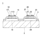
図1は、本発明に係る圧電デバイスを示す模式的な断面図である。圧電デバイス1は、第1の圧電共振子10と、第2の圧電共振子20と、基板2と、を備えている。
[First Embodiment]
FIG. 1 is a schematic cross-sectional view showing a piezoelectric device according to the present invention. The
基板2は、第1の圧電共振子10と、第2の圧電共振子20とを支持するために設けられている。基板2の材質の例としては、Si系基板や、絶縁性セラミックや絶縁性樹脂等の絶縁性材料が挙げられる。
The
第1の圧電共振子10と第2の圧電共振子20は、基板2の一方の主面の上に形成されている。第1の圧電共振子10は、圧電薄膜3と、圧電薄膜3の一方の主面に設けられた上部電極13と、他方の主面に設けられた下部電極11と、を有している。本実施形態では、下部電極11は、上部電極13よりも大きい面積となるように形成されている。同様に、第2の圧電共振子20は、圧電薄膜3と、圧電薄膜3の一方の主面に設けられた上部電極23と、他方の主面に設けられた下部電極21と、を有している。
The first
圧電振動部15は、上部電極13と下部電極11が圧電薄膜3を介して重なり合う部分で構成されている。圧電薄膜3の材質としては、例えばAlNが挙げられ、その分極方向は、圧電薄膜3の厚さ方向である。上部電極13と下部電極11に交流電圧が印加されると、厚み縦振動モードを利用した共振特性が得られる。この場合、圧電振動部15はエネルギー閉じ込め型の圧電振動部となる。圧電薄膜3の厚さは、例えば0.1μm〜10μmである。同様に、圧電振動部25は、上部電極23と下部電極21が圧電薄膜3を介して重なり合う部分で構成されている。
The piezoelectric vibrating
上部電極13、23及び下部電極11、21の材質は導電性材料であり、例えばW等の貴金属やAl等の卑金属が挙げられる。
The material of the
圧電振動部15、25は、基板2から音響的に分離されるように設けられている。本実施形態では、圧電振動部15、25は、空洞部19、29により基板2から浮いている状態で形成されている。圧電薄膜3は、空洞部19、29の周囲で、基板2の一方の主面上に固定されている。なお、圧電振動部15、25は、空洞部19、29の代わりに、音響反射層により基板2から音響的に分離されていても良い。
The piezoelectric vibrating
なお、空洞部19、29は、例えば、ZnOによる犠牲層の形成後に、ウェットエッチングにより犠牲層を除去して形成される。また、圧電薄膜3、上部電極13、23、及び下部電極11、21は、例えば、スパッタリングにより薄膜を形成した後、フォトリソグラフィによりパターニングをして形成される。
The
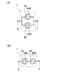
図2は、本発明に係る圧電デバイスが入力端子と出力端子に接続されている回路の模式図である。図2(A)は並列の例であり、図2(B)は直列の例である。 FIG. 2 is a schematic diagram of a circuit in which a piezoelectric device according to the present invention is connected to an input terminal and an output terminal. FIG. 2A is a parallel example, and FIG. 2B is a serial example.
図2(A)において、第1の圧電共振子10と第2の圧電共振子20とは、入力端子5と出力端子7との間で並列に接続されている。矢印10Rは、第1の圧電共振子10の圧電薄膜の分極方向を示している。また、矢印20Rは、第2の圧電共振子20の圧電薄膜の分極方向を示している。第1の圧電共振子10の分極方向10Rと第2の圧電共振子20の分極方向20Rは、入力端子5からみて互いに逆である。
In FIG. 2A, the first
同様に、図2(B)は直列の例であり、第1の圧電共振子10と第2の圧電共振子20とは、入力端子5と出力端子7との間で直列に接続されている。そして、第1の圧電共振子10の分極方向10Rと第2の圧電共振子20の分極方向20Rは、入力端子5からみて互いに逆である。
Similarly, FIG. 2B is an example in series, and the first
直列接続と並列接続を比較すると、同じインピーダンスの2つの圧電共振子を接続した場合には、並列接続のインピーダンスは直列接続の4倍となる。したがって、直列接続と並列接続で同じインピーダンスにする場合には、並列接続は直列接続の1/4の面積で良いため、並列接続の方が小型化できるという利点を有する。 Comparing series connection and parallel connection, when two piezoelectric resonators having the same impedance are connected, the impedance of the parallel connection is four times that of the series connection. Therefore, in the case where the same impedance is set for the series connection and the parallel connection, the parallel connection may have an area that is ¼ of that of the series connection, so that the parallel connection has an advantage that the size can be reduced.
本発明では、第1の圧電共振子10と第2の圧電共振子20とは、横振動モードの共振周波数が互いに異なるように形成されている。第1の圧電共振子10と第2の圧電共振子20には、厚み縦振動モードによる共振の他に、圧電薄膜3の面方向に伝搬する横振動モードによるリップルが発生し、このリップルが互いに強めあうという問題が生じていた。そのため、本発明のように、横振動モードの共振周波数が互いに異なるように形成されることにより、リップルが互いに強めあうことがなく、良好な共振特性やフィルタ特性の圧電デバイスが得られる。
In the present invention, the first
第1の圧電共振子10と第2の圧電共振子20とは、厚み縦振動モードの共振周波数が等しいことが好ましい。この場合には、どちらもインピーダンスが等しくなり、リップルが互いに強めやすくなるため、発明の効果が顕著である。
It is preferable that the first
図1のように、圧電振動部15の主面の周辺部の少なくとも一部には、音速変化膜17が形成されている。また、圧電振動部25の主面の周辺部の少なくとも一部には、音速変化膜27が形成されている。本実施形態では、音速変化膜17、27は帯状に形成されており、互いに線幅が異なる。そのため、第1の圧電共振子10と第2の圧電共振子20は、横振動モードの共振周波数が互いに異なり、横振動モードのリップルが互いに強めあうことを防いでいる。線幅を変える場合には、スパッタリングとフォトリソグラフィを用いる場合に、マスクパターンを変更するだけで良いので、簡単に製造することができる。
As shown in FIG. 1, a sound
本実施形態において、音速変化膜17、27の材質は同じである。音速変化膜17、27の材質の例としては、上部電極13、23や下部電極21、21と同じ導電性材料が挙げられる。また、SiO2等の絶縁性材料であっても良い。
In the present embodiment, the sound
また、本実施形態では、音速変化膜17は、圧電振動部15の周縁に接するように形成されている。この場合には、横振動モードのリップルをより効果的に抑えることができる。音速変化膜27も同様である。
In the present embodiment, the sound
また、本実施形態では、音速変化膜17は、上部電極13上に形成されている。この場合には、音速変化膜17が形成しやすいという利点を有する。音速変化膜27も同様である。
In the present embodiment, the sound
図3は、本発明に係る圧電デバイスに用いられる圧電振動部15、25と音速変化膜17、27の模式的な平面図である。上部電極13上に形成されている音速変化膜17は、上部電極13の周縁に沿って閉じた帯状に形成されている。この場合には、横振動モードのリップルをより効果的に抑えることができる。音速変化膜27も同様である。
FIG. 3 is a schematic plan view of the piezoelectric vibrating
また、図3では、音速変化膜17、27は、上面視したときに音速変化膜17、27の取り囲む図形の面積が同じで、かつ、形状が異なるように形成されている。この場合には、それぞれの圧電振動部の圧電薄膜が同じ材質で厚さであれば、面積が同じであるので圧電振動部の厚み縦振動モードの共振周波数が等しくなり、本発明の効果が顕著になる。
In FIG. 3, the sound
また、図3では、音速変化膜17、27は、上面視したときに音速変化膜17、27の取り囲む図形が、平行な二辺がない多角形状に形成されている。この場合には、平行な二辺がないため、横振動モードの定在波が発生しにくいという利点を有する。
In FIG. 3, the sound
なお、本実施形態の圧電デバイスは2個の圧電振動子を備えているが、4個や6個等の偶数個の圧電共振子を備えていても良い。その場合、入力端子からみた分極方向の向きが正方向である圧電振動子の数と、逆方向である圧電振動子の数が同じであれば、本発明の効果を奏する。 Although the piezoelectric device of this embodiment includes two piezoelectric vibrators, it may include an even number of piezoelectric resonators such as four or six. In this case, the effect of the present invention can be obtained if the number of piezoelectric vibrators whose polarization direction as viewed from the input terminal is the same as the number of piezoelectric vibrators in the reverse direction.
また、本実施形態では、圧電薄膜3は第1の圧電共振子10と第2の圧電共振子20の間を一部が連なるように形成されているが、第1の圧電共振子10と第2の圧電共振子10で分離して別々に形成されていても良い。
In the present embodiment, the piezoelectric
また、本実施形態では、音速変化膜17、27は閉じた帯状であるが、圧電振動部15、25の、主面の周辺部の少なくとも一部に形成されていれば良い。例えば、閉じた帯状である音速変化膜17、27の一部に切り込みが形成されていても良いし、上部電極の一部の辺だけに形成されていても良い。
In the present embodiment, the sound
また、本実施形態では、音速変化膜17、27は上部電極13、23上に形成されているが、下部電極11、21の下に形成されていても良い。また、上部電極13、23と圧電薄膜3の間や、下部電極11、21と圧電薄膜3の間に形成されていても良い。
In the present embodiment, the sound
また、本実施形態では、音速変化膜17、27は圧電振動部15、25の周縁に接するように形成されているが、周縁を含むように形成されていても良い。
In the present embodiment, the sound
また、本実施形態では、上部電極13、23と下部電極11、21は単層構造であるが、例えば、導電成分を主成分とする電極層と下地層とが積層された積層構造であっても良い。
In this embodiment, the
[第2の実施形態]
図4は、本発明に係る圧電デバイスを示す模式的な断面図である。第1の実施形態と共通する部分については記載を省略する。本実施形態では、音速変化膜17、27は互いに厚さが異なっている。そのため、横振動モードの共振周波数が互いに異なり、リップルが互いに強めあうことを防いでいる。
[Second Embodiment]
FIG. 4 is a schematic cross-sectional view showing a piezoelectric device according to the present invention. Description of parts common to the first embodiment is omitted. In the present embodiment, the sound
[第3の実施形態]
図5は、本発明に係る圧電デバイスを示す模式的な断面図である。本実施形態では、音速変化膜17、27は互いに材質が異なっている。例えば、W、Mo、Ru、Ir、Al、Cu、Au、Pt、SiO2、AlN、Al2O3、Si3N4などの各種の金属材料、絶縁体材料の中から異なる2つを選択する。そのため、横振動モードの共振周波数が互いに異なり、リップルが互いに強めあうことを防いでいる。
[Third Embodiment]
FIG. 5 is a schematic cross-sectional view showing a piezoelectric device according to the present invention. In the present embodiment, the sound
[第4の実施形態]
図6は、本発明に係る圧電デバイスを示す模式的な断面図である。本実施形態では、第1の圧電共振子10と第2の圧電共振子20のうち、一方の圧電共振子10の主面の周辺部の少なくとも一部に音速変化膜17が形成されている。この場合においても、横振動モードの共振周波数を互いに異ならせることが可能である。
[Fourth Embodiment]
FIG. 6 is a schematic cross-sectional view showing a piezoelectric device according to the present invention. In the present embodiment, the sound
なお、本発明は上記の実施形態に限定されるものではなく、要旨を逸脱しない範囲において種々の変形が可能である。 In addition, this invention is not limited to said embodiment, A various deformation | transformation is possible in the range which does not deviate from a summary.
[実験例]
本発明の効果を、シミュレーションにより確認した。図7は、実験例のシミュレーションに用いる圧電共振子10を示す模式的な断面図である。上部電極13と下部電極11の形状は円形であり、圧電振動部15の周縁に沿って、音速変化膜27が閉じた帯状で形成されている圧電共振子を想定した。そして、音速変化膜27の線幅(図7中のX)を1〜3μmの幅で変化させた場合における、インピーダンスと位相の変化を確認した。なお、シミュレーションの条件は下記の通りである。
音速変化膜 材質 タングステン(W)
厚さ 100nm
上部電極 材質 タングステン(W)
厚さ 600nm
圧電層 材質 窒化アルミニウム(AlN)
厚さ 1600nm
下部電極 材質 タングステン(W)
厚さ 600nm
圧電共振子 面積 44000μm2
[Experimental example]
The effect of the present invention was confirmed by simulation. FIG. 7 is a schematic cross-sectional view showing the
Sound velocity change material Tungsten (W)
Thickness 100nm
Upper electrode material Tungsten (W)
600nm thickness
Piezoelectric layer Material Aluminum nitride (AlN)
Thickness 1600nm
Lower electrode material Tungsten (W)
600nm thickness
Piezoelectric resonator Area 44000μm 2
図8は、図7の圧電共振子の音速変化膜の線幅を変化させた場合の、インピーダンスと位相を示す図である。図8(A)は線幅が1μm、図8(B)は線幅が2μm、図8(C)は線幅が3μmの図である。 FIG. 8 is a diagram showing impedance and phase when the line width of the sound velocity changing film of the piezoelectric resonator of FIG. 7 is changed. 8A shows a line width of 1 μm, FIG. 8B shows a line width of 2 μm, and FIG. 8C shows a line width of 3 μm.
図8(A)〜(C)を比較すると、音速変化膜の線幅を変化させた場合には、通過帯域の周波数や、通過帯域外のインピーダンスはほとんど変化しない。一方、圧電共振子の通過帯域内のリップルの周波数や強度は、音速変化膜の線幅に応じて変化する。したがって、音速変化膜の線幅の異なる圧電共振子を組み合わせることにより、互いのリップルが重ならないようにすることが可能である。 8A to 8C, when the line width of the sound speed change film is changed, the frequency in the pass band and the impedance outside the pass band hardly change. On the other hand, the frequency and intensity of the ripple in the passband of the piezoelectric resonator change according to the line width of the sound velocity changing film. Therefore, it is possible to prevent the ripples from overlapping each other by combining piezoelectric resonators having different line widths of the sound velocity change film.
1 圧電デバイス
2 基板
3 圧電薄膜
5 入力端子
7 出力端子
10 第1の圧電共振子
10R 矢印
11 下部電極
13 上部電極
15 圧電振動部
17 音速変化膜
19 空洞部
20 第2の圧電共振子
20R 矢印
21 下部電極
23 上部電極
25 圧電振動部
27 音速変化膜
29 空洞部
172 第1のBAW共振子
172R 矢印
174 第2のBAW共振子
174R 矢印
176 第1の電気端子
178 第2の電気端子
DESCRIPTION OF
Claims (12)
前記第1の圧電共振子と前記第2の圧電共振子とは、横モードの共振周波数が互いに異なるように形成されている、圧電デバイス。 A piezoelectric thin film, an upper electrode provided on one main surface of the piezoelectric thin film, and a lower electrode provided on the other main surface of the piezoelectric thin film, and in series between an input terminal and an output terminal A first piezoelectric resonator and a second piezoelectric resonator connected in parallel so that the polarization directions of the piezoelectric thin film viewed from the input terminal are opposite to each other;
The piezoelectric device, wherein the first piezoelectric resonator and the second piezoelectric resonator are formed so that resonance frequencies of transverse modes are different from each other.
前記第1の圧電共振子と前記第2の圧電共振子のうち少なくとも一方の圧電振動部の、主面の周辺部の少なくとも一部に音速変化膜が形成されている、請求項1または2に記載の圧電デバイス。 The first piezoelectric resonator and the second piezoelectric resonator are configured such that a piezoelectric vibrating portion is formed at a portion where the upper electrode and the lower electrode overlap with each other through the piezoelectric thin film so as to be acoustically separated from the substrate. Has been
The sound velocity change film is formed on at least a part of a peripheral portion of the main surface of at least one of the first piezoelectric resonator and the second piezoelectric resonator. The piezoelectric device described.
前記第1の圧電共振子と前記第2の圧電共振子のそれぞれの圧電振動部の、主面の周辺部の少なくとも一部に音速変化膜が形成されている、請求項1または2に記載の圧電デバイス。 The first piezoelectric resonator and the second piezoelectric resonator are configured such that a piezoelectric vibrating portion is formed at a portion where the upper electrode and the lower electrode overlap with each other through the piezoelectric thin film so as to be acoustically separated from the substrate. Has been
3. The sound velocity change film according to claim 1, wherein a sound velocity change film is formed on at least a part of a peripheral portion of a main surface of each piezoelectric vibration portion of each of the first piezoelectric resonator and the second piezoelectric resonator. Piezoelectric device.
Priority Applications (2)
| Application Number | Priority Date | Filing Date | Title |
|---|---|---|---|
| JP2011015825A JP5360432B2 (en) | 2011-01-27 | 2011-01-27 | Piezoelectric device |
| US13/348,033 US8878419B2 (en) | 2011-01-27 | 2012-01-11 | Piezoelectric device |
Applications Claiming Priority (1)
| Application Number | Priority Date | Filing Date | Title |
|---|---|---|---|
| JP2011015825A JP5360432B2 (en) | 2011-01-27 | 2011-01-27 | Piezoelectric device |
Publications (2)
| Publication Number | Publication Date |
|---|---|
| JP2012156907A true JP2012156907A (en) | 2012-08-16 |
| JP5360432B2 JP5360432B2 (en) | 2013-12-04 |
Family
ID=46576767
Family Applications (1)
| Application Number | Title | Priority Date | Filing Date |
|---|---|---|---|
| JP2011015825A Active JP5360432B2 (en) | 2011-01-27 | 2011-01-27 | Piezoelectric device |
Country Status (2)
| Country | Link |
|---|---|
| US (1) | US8878419B2 (en) |
| JP (1) | JP5360432B2 (en) |
Cited By (5)
| Publication number | Priority date | Publication date | Assignee | Title |
|---|---|---|---|---|
| JP2013123184A (en) * | 2011-12-12 | 2013-06-20 | Taiyo Yuden Co Ltd | Filter and duplexer |
| JP2017135463A (en) * | 2016-01-25 | 2017-08-03 | 太陽誘電株式会社 | Acoustic wave device |
| JP2018037906A (en) * | 2016-08-31 | 2018-03-08 | 太陽誘電株式会社 | Piezoelectric thin film resonator, filter, and multiplexer |
| KR20180048244A (en) * | 2016-10-31 | 2018-05-10 | 삼성전기주식회사 | Filter including acoustic wave resonator |
| WO2022042756A1 (en) * | 2020-08-24 | 2022-03-03 | 苏州奥谱毫通电子科技有限公司 | Crystal filter element and manufacturing method therefor |
Families Citing this family (4)
| Publication number | Priority date | Publication date | Assignee | Title |
|---|---|---|---|---|
| US11469735B2 (en) * | 2018-11-28 | 2022-10-11 | Taiyo Yuden Co., Ltd. | Acoustic wave device, filter, and multiplexer |
| CN109768781A (en) * | 2018-12-25 | 2019-05-17 | 天津大学 | Split type resonator |
| CN109818593B (en) * | 2018-12-25 | 2023-10-03 | 天津大学 | Split resonator with different impedance ratio |
| CN111262548B (en) * | 2019-12-31 | 2021-06-22 | 诺思(天津)微系统有限责任公司 | Bulk acoustic wave resonator group, filter, electronic device, and electromechanical coupling coefficient adjustment method |
Citations (12)
| Publication number | Priority date | Publication date | Assignee | Title |
|---|---|---|---|---|
| WO1999037023A1 (en) * | 1998-01-16 | 1999-07-22 | Mitsubishi Denki Kabushiki Kaisha | Thin film pietoelectric element |
| JP2005159402A (en) * | 2003-11-20 | 2005-06-16 | Matsushita Electric Ind Co Ltd | Acoustic resonator |
| JP2005176332A (en) * | 2003-11-20 | 2005-06-30 | Matsushita Electric Ind Co Ltd | Piezoelectric element, composite piezoelectric element, and filter, duplexer and communication equipment using the same |
| JP2007006486A (en) * | 2005-06-20 | 2007-01-11 | Avago Technologies General Ip (Singapore) Private Ltd | Suspended device and its manufacturing method |
| JP2007006495A (en) * | 2005-06-22 | 2007-01-11 | Infineon Technologies Ag | Baw device |
| JP2007510374A (en) * | 2003-10-30 | 2007-04-19 | アバゴ・テクノロジーズ・ジェネラル・アイピー(シンガポール)プライベート・リミテッド | Control of impedance conversion ratio in thin film acoustic coupling transformer. |
| JP2007300216A (en) * | 2006-04-27 | 2007-11-15 | Fujitsu Media Device Kk | Filter and demultiplexer |
| JP2008085989A (en) * | 2006-09-01 | 2008-04-10 | Fujitsu Media Device Kk | Acoustic wave device, filter and duplexer |
| JP2008219237A (en) * | 2007-03-01 | 2008-09-18 | Seiko Epson Corp | Bulk acoustic resonator |
| JP2009010932A (en) * | 2007-04-16 | 2009-01-15 | Avago Technologies General Ip (Singapore) Private Ltd | Bulk acoustic wave (baw) filter having reduced second harmonic generation and method of reducing second harmonic generation in baw filter |
| JP2009188939A (en) * | 2008-02-08 | 2009-08-20 | Tdk Corp | Thin film bulk wave acoustic resonator |
| JP2010021914A (en) * | 2008-07-14 | 2010-01-28 | Murata Mfg Co Ltd | Demultiplexer |
Family Cites Families (3)
| Publication number | Priority date | Publication date | Assignee | Title |
|---|---|---|---|---|
| US7280007B2 (en) * | 2004-11-15 | 2007-10-09 | Avago Technologies General Ip (Singapore) Pte. Ltd. | Thin film bulk acoustic resonator with a mass loaded perimeter |
| JP2006319796A (en) * | 2005-05-13 | 2006-11-24 | Toshiba Corp | Thin film bulk wave acoustic resonator |
| JP4661958B2 (en) * | 2006-04-05 | 2011-03-30 | 株式会社村田製作所 | Piezoelectric resonator and piezoelectric filter |
-
2011
- 2011-01-27 JP JP2011015825A patent/JP5360432B2/en active Active
-
2012
- 2012-01-11 US US13/348,033 patent/US8878419B2/en active Active
Patent Citations (12)
| Publication number | Priority date | Publication date | Assignee | Title |
|---|---|---|---|---|
| WO1999037023A1 (en) * | 1998-01-16 | 1999-07-22 | Mitsubishi Denki Kabushiki Kaisha | Thin film pietoelectric element |
| JP2007510374A (en) * | 2003-10-30 | 2007-04-19 | アバゴ・テクノロジーズ・ジェネラル・アイピー(シンガポール)プライベート・リミテッド | Control of impedance conversion ratio in thin film acoustic coupling transformer. |
| JP2005159402A (en) * | 2003-11-20 | 2005-06-16 | Matsushita Electric Ind Co Ltd | Acoustic resonator |
| JP2005176332A (en) * | 2003-11-20 | 2005-06-30 | Matsushita Electric Ind Co Ltd | Piezoelectric element, composite piezoelectric element, and filter, duplexer and communication equipment using the same |
| JP2007006486A (en) * | 2005-06-20 | 2007-01-11 | Avago Technologies General Ip (Singapore) Private Ltd | Suspended device and its manufacturing method |
| JP2007006495A (en) * | 2005-06-22 | 2007-01-11 | Infineon Technologies Ag | Baw device |
| JP2007300216A (en) * | 2006-04-27 | 2007-11-15 | Fujitsu Media Device Kk | Filter and demultiplexer |
| JP2008085989A (en) * | 2006-09-01 | 2008-04-10 | Fujitsu Media Device Kk | Acoustic wave device, filter and duplexer |
| JP2008219237A (en) * | 2007-03-01 | 2008-09-18 | Seiko Epson Corp | Bulk acoustic resonator |
| JP2009010932A (en) * | 2007-04-16 | 2009-01-15 | Avago Technologies General Ip (Singapore) Private Ltd | Bulk acoustic wave (baw) filter having reduced second harmonic generation and method of reducing second harmonic generation in baw filter |
| JP2009188939A (en) * | 2008-02-08 | 2009-08-20 | Tdk Corp | Thin film bulk wave acoustic resonator |
| JP2010021914A (en) * | 2008-07-14 | 2010-01-28 | Murata Mfg Co Ltd | Demultiplexer |
Cited By (6)
| Publication number | Priority date | Publication date | Assignee | Title |
|---|---|---|---|---|
| JP2013123184A (en) * | 2011-12-12 | 2013-06-20 | Taiyo Yuden Co Ltd | Filter and duplexer |
| JP2017135463A (en) * | 2016-01-25 | 2017-08-03 | 太陽誘電株式会社 | Acoustic wave device |
| US11038486B2 (en) | 2016-01-25 | 2021-06-15 | Taiyo Yuden Co., Ltd. | Acoustic wave device |
| JP2018037906A (en) * | 2016-08-31 | 2018-03-08 | 太陽誘電株式会社 | Piezoelectric thin film resonator, filter, and multiplexer |
| KR20180048244A (en) * | 2016-10-31 | 2018-05-10 | 삼성전기주식회사 | Filter including acoustic wave resonator |
| WO2022042756A1 (en) * | 2020-08-24 | 2022-03-03 | 苏州奥谱毫通电子科技有限公司 | Crystal filter element and manufacturing method therefor |
Also Published As
| Publication number | Publication date |
|---|---|
| JP5360432B2 (en) | 2013-12-04 |
| US8878419B2 (en) | 2014-11-04 |
| US20120194034A1 (en) | 2012-08-02 |
Similar Documents
| Publication | Publication Date | Title |
|---|---|---|
| JP5360432B2 (en) | Piezoelectric device | |
| JP4252584B2 (en) | Piezoelectric thin film resonator and filter | |
| US9093979B2 (en) | Laterally-coupled acoustic resonators | |
| KR101242314B1 (en) | Piezoelectric thin film resonant element and circuit component using the same | |
| JP4803183B2 (en) | Piezoelectric thin film resonator | |
| US7649304B2 (en) | Piezoelectric resonator and piezoelectric filter | |
| US8575820B2 (en) | Stacked bulk acoustic resonator | |
| KR100631217B1 (en) | Integrated filter comprising fbar and saw resonator and fabrication method therefor | |
| JP4944145B2 (en) | Piezoelectric thin film resonator, filter, communication module, communication device | |
| WO2016052129A1 (en) | Acoustic wave device and method for manufacturing same | |
| JP4428354B2 (en) | Piezoelectric thin film resonator | |
| WO2011099319A1 (en) | Piezoelectric thin-film resonator, communication module and communication device | |
| JP2008048380A (en) | Resonator and manufacturing | |
| JPWO2016111315A1 (en) | Elastic wave device | |
| JP4775445B2 (en) | Thin film piezoelectric resonator and thin film piezoelectric filter | |
| JP5040172B2 (en) | Thin film piezoelectric resonator and thin film piezoelectric filter | |
| JP5390431B2 (en) | Elastic wave device | |
| CN110313130A (en) | Surface acoustic wave device | |
| JP2007288504A (en) | Piezoelectric thin film resonator | |
| JP5204258B2 (en) | Method for manufacturing piezoelectric thin film resonator | |
| WO2016039026A1 (en) | Surface acoustic wave device | |
| JP2009100467A (en) | Resonance apparatus | |
| JP2006333296A (en) | Surface acoustic wave device | |
| JP2013012932A (en) | Acoustic wave device and method for manufacturing the same | |
| JP2008141561A (en) | Resonator filter |
Legal Events
| Date | Code | Title | Description |
|---|---|---|---|
| A621 | Written request for application examination |
Free format text: JAPANESE INTERMEDIATE CODE: A621 Effective date: 20121024 |
|
| A131 | Notification of reasons for refusal |
Free format text: JAPANESE INTERMEDIATE CODE: A131 Effective date: 20130305 |
|
| A521 | Request for written amendment filed |
Free format text: JAPANESE INTERMEDIATE CODE: A523 Effective date: 20130426 |
|
| TRDD | Decision of grant or rejection written | ||
| A01 | Written decision to grant a patent or to grant a registration (utility model) |
Free format text: JAPANESE INTERMEDIATE CODE: A01 Effective date: 20130807 |
|
| A61 | First payment of annual fees (during grant procedure) |
Free format text: JAPANESE INTERMEDIATE CODE: A61 Effective date: 20130820 |
|
| R150 | Certificate of patent or registration of utility model |
Ref document number: 5360432 Country of ref document: JP Free format text: JAPANESE INTERMEDIATE CODE: R150 Free format text: JAPANESE INTERMEDIATE CODE: R150 |