JP2012156336A - Optical integrated circuit - Google Patents
Optical integrated circuit Download PDFInfo
- Publication number
- JP2012156336A JP2012156336A JP2011014531A JP2011014531A JP2012156336A JP 2012156336 A JP2012156336 A JP 2012156336A JP 2011014531 A JP2011014531 A JP 2011014531A JP 2011014531 A JP2011014531 A JP 2011014531A JP 2012156336 A JP2012156336 A JP 2012156336A
- Authority
- JP
- Japan
- Prior art keywords
- semiconductor
- optical
- mach
- zehnder modulator
- integrated circuit
- Prior art date
- Legal status (The legal status is an assumption and is not a legal conclusion. Google has not performed a legal analysis and makes no representation as to the accuracy of the status listed.)
- Granted
Links
Images


Abstract
Description
本発明は、光集積回路に関し、より詳細には、半導体レーザと半導体マッハツェンダ変調器とを集積した光集積回路に関する。 The present invention relates to an optical integrated circuit, and more particularly to an optical integrated circuit in which a semiconductor laser and a semiconductor Mach-Zehnder modulator are integrated.
近年の光通信網の普及に伴い、40Gbit/sec(ギガビット毎秒)を超える伝送容量を有する基幹系光通信システムへの適応が盛んに進められるようになった。これらの超高速光通信システムでは、従来の光通信システムで適用されてきたNRZ(Non Return to Zero)変調方式と比べて、周波数利用効率が高く、また光信号対雑音比(Optical Signal−to−Noise Ratio:OSNR)耐力および非線形性耐力等の優れた様々な光変調方式の採用が相次いでいる。このような背景の中、1シンボル時間で多ビット情報を送信する方式が最も有力な手段として考えられている。 With the recent spread of optical communication networks, adaptation to backbone optical communication systems having a transmission capacity exceeding 40 Gbit / sec (Gigabit per second) has been actively promoted. These ultra-high-speed optical communication systems have higher frequency utilization efficiency and optical signal-to-noise ratio (Optical Signal-to-To--) compared to NRZ (Non Return to Zero) modulation schemes that have been applied in conventional optical communication systems. Adoption of various light modulation schemes such as Noise Ratio (OSNR) proof strength and non-linear proof strength has been continued. In such a background, a method of transmitting multi-bit information in one symbol time is considered as the most effective means.
例えば、変調された4つの位相に各2ビットのデータを割り当て可能な方式である差動四相位相偏移変調(differential quadrature phase shift keying:DQPSK)の場合、送信器としては、少なくとも4つの高速位相変調器を集積したデバイス構成が必要となる。現在これらの高速位相変調器には、ニオブ酸リチウム(LiNbO3:LN)で構成されたLN導波路上にLN変調器を設けたものが広く用いられている(以下、LN変調器が設けられたLN導波路全体を「LN導波路」という。)。LN導波路を用いることで、低損失にこれらの光変調器を実現することができるメリットがある。しかしながら、より複雑な情報伝送フォーマットにLN導波路を用いて対応する場合、デバイスサイズが大きくなるというデメリットを生ずる。例えば、100Gbit/secを実現するために、各位相に偏波多重を含めた4ビットのデータを割り当てるDP-QPSK(Dual Polarization Quadrature Phase Shift Keying)を採用した場合、送信器は、偏波毎にDQPSKの構成を備えた形となる。これをLN導波路を用いて形成した場合、必要なカップラーの個数も増える上、位相変調器の個数が少なくとも8個とDQPSKの2倍になるため、素子サイズが非常に大きくなる問題がある。今後、さらにDP-QPSK以上に複雑な情報伝送フォーマットに対応しようとすると、LN導波路ではデバイスサイズが非常に大きくなってしまう。 For example, in the case of differential quadrature phase shift keying (DQPSK), which is a method capable of allocating 2-bit data to four modulated phases, at least four high-speed transmitters are used. A device configuration in which a phase modulator is integrated is required. At present, these high-speed phase modulators are widely used in which an LN modulator is provided on an LN waveguide made of lithium niobate (LiNbO 3 : LN) (hereinafter referred to as an LN modulator). The entire LN waveguide is referred to as “LN waveguide”). By using the LN waveguide, there is an advantage that these optical modulators can be realized with low loss. However, when dealing with a more complicated information transmission format using the LN waveguide, there is a demerit that the device size is increased. For example, in order to realize 100 Gbit / sec, when adopting DP-QPSK (Dual Polarization Quadrature Phase Shift Keying) in which 4-bit data including polarization multiplexing is included in each phase, the transmitter is provided for each polarization. It becomes the form provided with the structure of DQPSK. When this is formed using an LN waveguide, the number of required couplers increases, and the number of phase modulators is at least eight, which is twice that of DQPSK, resulting in a problem that the element size becomes very large. In the future, if an attempt is made to cope with a more complicated information transmission format than DP-QPSK, the device size will become very large in the LN waveguide.
また、LN導波路を収めたモジュール内では、半導体レーザ等の光源が別に用意され、それらをファイバーで接続する形が取られる。そのため、光源およびファイバーの分だけ必然的にモジュールサイズが大きくなってしまうだけでなく、余長ファイバーの格納にもスペースを要する。これらを解決する手法としては、光源とLN導波路を同じパッケージ内に収めることが考えられるが、LN導波路と光源では構成する材料が異なるため、熱膨張係数の違い等から必ずしも容易ではない。 Also, in the module containing the LN waveguide, a light source such as a semiconductor laser is separately prepared and connected by a fiber. Therefore, not only the module size is inevitably increased by the amount of the light source and the fiber, but also a space is required for storing the extra length fiber. As a method for solving these problems, it is conceivable that the light source and the LN waveguide are housed in the same package. However, since the materials constituting the LN waveguide and the light source are different, it is not always easy due to a difference in thermal expansion coefficient.
DP-QPSKを例とすると、両偏波用のマッハツェンダ干渉計に同一波長で、かつ位相がランダムでない光を入力する必要があり、通常は、LN導波路に入力される半導体単一モード発振レーザからの出力光が、LN導波路上に設けられたパワースプリッタにて二等分され、各マッハツェンダ干渉計に入射されることになる。 Taking DP-QPSK as an example, it is necessary to input light having the same wavelength and non-random phase to a Mach-Zehnder interferometer for both polarizations. Usually, a semiconductor single mode oscillation laser input to an LN waveguide The output light from is divided into two equal parts by a power splitter provided on the LN waveguide, and is incident on each Mach-Zehnder interferometer.
光源として用いられる半導体単一モード発振レーザは、代表的には、発振スペクトルの線幅が狭い分布帰還型レーザ(Distributed FeedBack laser:DFBレーザ)が多く用いられる。特に、λ/4シフトDFBレーザが用いられることが多い。原理上、λ/4シフトを共振器構造の中央に配置した場合は、無反射構造のレーザ両端に出力される光強度が等しくなる。通常λ/4シフトの位置をややずらすことにより、共振器構造内での光強度が非対称化し、前方からの光出力が強くなるように調整される。しかしながら、λ/4シフトの位置を調整して得られる非対称性は小さい。つまり、共振器構造の中央付近に配置した場合を考えると、ほぼ半分にあたる後方の光出力を捨てる構造なのである。 As a semiconductor single mode oscillation laser used as a light source, a distributed feedback laser (DFB laser) having a narrow oscillation spectrum linewidth is typically used. In particular, a λ / 4 shift DFB laser is often used. In principle, when the λ / 4 shift is arranged at the center of the resonator structure, the light intensities output to both ends of the laser of the non-reflective structure are equal. Usually, by slightly shifting the position of the λ / 4 shift, the light intensity in the resonator structure is asymmetrical, and the light output from the front is adjusted to be strong. However, the asymmetry obtained by adjusting the position of the λ / 4 shift is small. In other words, considering the case where it is arranged near the center of the resonator structure, it is a structure in which the rear light output, which is almost half, is discarded.
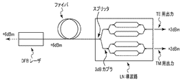
図1に、LN導波路を用いたDP-QPSKにおける光パワー出力の概算を模式的に示す。現実的にはあり得ないが、LN導波路上での損失、および各光部品を接続する接続損失がゼロであると仮定する。TE偏波用およびTM偏波用のLN導波路の出力に3dBmが必要だったとすると、LN導波路に入射する光強度は、6dBm必要ということになる。そして半導体レーザの出力も結合損失がゼロと仮定すると同じだけ必要となる。しかしながら、DFBレーザ等のレーザ光源を想定すると、後方に破棄される光出力がそれと同様に6dBm程度存在するので、エネルギーの利用効率が低い。実際は5dB程度のLN変調器の挿入損失、1.5dB程度のレーザとファイバーの結合損失などが加わるため、さらに高出力が求められることになり、それに付随して後方への破棄分も増加することになる。 FIG. 1 schematically shows an approximate optical power output in DP-QPSK using an LN waveguide. Although it is impossible in practice, it is assumed that the loss on the LN waveguide and the connection loss connecting each optical component are zero. If 3 dBm is required for the output of the TE polarization and TM polarization LN waveguides, the light intensity incident on the LN waveguide is 6 dBm. If the coupling loss is assumed to be zero, the same amount of output from the semiconductor laser is required. However, assuming a laser light source such as a DFB laser, the energy output efficiency is low because the light output discarded behind is about 6 dBm. Actually, an insertion loss of an LN modulator of about 5 dB and a coupling loss between a laser and a fiber of about 1.5 dB are added, so that a higher output is required, and the amount of backward discard increases accordingly. become.
なお、図1ではLN導波路から出た光を両偏波用の出力として示しているが、実際は片方の偏波のみがLN導波路内で導波しており、同じ偏波である。このうち一方を半波長板を通過させ偏波を回転させてから、偏波合波し出力する。 In FIG. 1, the light emitted from the LN waveguide is shown as an output for both polarizations, but only one polarization is actually guided in the LN waveguide and has the same polarization. One of them passes through the half-wave plate and rotates the polarization, and then combines and outputs the polarization.
LN導波路で構成した変調器のサイズが大きいという問題を回避するために、半導体で光導波路を構成し、電界を半導体素子に与えたときに主としてポッケルス効果で生じる屈折率変化を利用して入力電気信号を光の位相変化に変換する、マッハツェンダ型光変調器(以下「半導体マッハツェンダ変調器」という。)が注目されている。半導体マッハツェンダ変調器は、LN導波路に比べて導波路を構成する材料の比屈折率差が大きいため、曲げ半径を小さくでき、小型な回路レイアウトが可能となる。すでに、DQPSK等の多値伝送フォーマットに対応した高速変調器が報告されている(非特許文献1参照)。 In order to avoid the problem that the size of the modulator composed of the LN waveguide is large, an optical waveguide is composed of a semiconductor, and input is performed using the refractive index change mainly caused by the Pockels effect when an electric field is applied to the semiconductor element. Mach-Zehnder type optical modulators (hereinafter referred to as “semiconductor Mach-Zehnder modulators”) that convert electrical signals into light phase changes have attracted attention. Since the semiconductor Mach-Zehnder modulator has a larger relative refractive index difference between materials constituting the waveguide than the LN waveguide, the bending radius can be reduced, and a small circuit layout can be achieved. A high-speed modulator corresponding to a multilevel transmission format such as DQPSK has already been reported (see Non-Patent Document 1).
また、半導体マッハツェンダ変調器のさらなる利点は、レーザ光源と1つのチップ上に集積が可能という点がある。集積することで、半導体レーザ・半導体マッハツェンダ変調器間の接続損失が低減できるだけでなく、余長ファイバー処理が不要で、小型というメリットが得られる。 Another advantage of the semiconductor Mach-Zehnder modulator is that it can be integrated on a single chip with the laser light source. By integrating, not only the connection loss between the semiconductor laser and the semiconductor Mach-Zehnder modulator can be reduced, but also the extra length fiber processing is unnecessary, and the advantage of small size can be obtained.
半導体レーザと半導体マッハツェンダ変調器とを集積した光集積回路の具体例として、InP基板を用いた例でより詳細に説明する。なお、以下の説明はInPも属する閃亜鉛鉱型結晶全般に言えることであり、同じ結晶系であるGaAs等でも同様になる。(100)面を有するInP基板上に半導体レーザを作製する場合、一般には[011]方向に半導体レーザの活性層導波路を作製するのが望ましい。様々なレーザ構造があるが、低閾値かつ高出力を可能とする埋め込み型半導体レーザを作製する場合には、活性層を有するメサ構造を[011]方向に作製しないと再成長による埋め込みが困難である。一方、ポッケルス効果による屈折率変化と量子閉じ込めシュタルク効果(Quantum Confined Stark Effect:QCSE)による屈折率変化とを併せて用いる、活性領域に多重量子井戸層(Multiple Quantum Well:MQW)をもつ半導体マッハツェンダ変調器は、[01−1]方向に作製すると電界を印加したときのポッケルス効果による屈折率変化がQCSEによる屈折率変化を強めるように変化し、一方で[011]方向に作製すると弱めるように変化する。よって、半導体マッハツェンダ変調器は、[01−1]方向に作製した方が変調効率がよくなり、その分だけ電界強度を下げたり変調器の素子長を短くしたりできるため、高速変調動作に有利になる。つまり、半導体レーザに適した面方位と、半導体マッハツェンダ変調器に適した面方位がそれぞれあり、集積化は面方位をも考慮した設計が必要となる。 As a specific example of an optical integrated circuit in which a semiconductor laser and a semiconductor Mach-Zehnder modulator are integrated, an example using an InP substrate will be described in more detail. The following explanation is applicable to all zinc blende type crystals to which InP also belongs, and the same applies to GaAs and the like which are the same crystal system. When fabricating a semiconductor laser on an InP substrate having a (100) plane, it is generally desirable to fabricate an active layer waveguide of the semiconductor laser in the [011] direction. There are various laser structures, but when fabricating a buried semiconductor laser capable of low threshold and high output, it is difficult to bury by re-growth unless a mesa structure having an active layer is fabricated in the [011] direction. is there. On the other hand, a semiconductor Mach-Zehnder modulation having a multiple quantum well layer (MQW) in the active region, using both a refractive index change due to the Pockels effect and a refractive index change due to the quantum confined Stark effect (QCSE). When the device is manufactured in the [01-1] direction, the refractive index change due to the Pockels effect when an electric field is applied changes so as to increase the refractive index change due to the QCSE, whereas when the device is manufactured in the [011] direction, the refractive index changes. To do. Therefore, the semiconductor Mach-Zehnder modulator is better manufactured in the [01-1] direction because the modulation efficiency is improved, and the electric field strength can be lowered correspondingly, and the element length of the modulator can be shortened. become. That is, there are a plane orientation suitable for a semiconductor laser and a plane orientation suitable for a semiconductor Mach-Zehnder modulator, respectively, and integration requires a design that also considers the plane orientation.
そこで、半導体レーザと半導体マッハツェンダ変調器とを集積した光集積回路において、半導体レーザが有するメサ構造の配置方向を、半導体マッハツェンダ変調器が有する2本のアーム導波路の配置方向とは異なる方向にすることが考えられている(特許文献1参照)。たとえば、半導体基板としてInP基板を用いる場合には、半導体レーザのメサ構造の配置方向を[011]方向に、半導体マッハツェンダ変調器のアーム導波路の配置方向を[01−1]方向とする。これにより、半導体レーザと半導体マッハツェンダ変調器が直線的に配置されていた場合と比較して、優れた変調特性を有する光集積回路が得られる。 Therefore, in an optical integrated circuit in which a semiconductor laser and a semiconductor Mach-Zehnder modulator are integrated, the arrangement direction of the mesa structure of the semiconductor laser is set to a direction different from the arrangement direction of the two arm waveguides of the semiconductor Mach-Zehnder modulator. (See Patent Document 1). For example, when an InP substrate is used as the semiconductor substrate, the arrangement direction of the mesa structure of the semiconductor laser is the [011] direction, and the arrangement direction of the arm waveguide of the semiconductor Mach-Zehnder modulator is the [01-1] direction. Thereby, an optical integrated circuit having excellent modulation characteristics can be obtained as compared with the case where the semiconductor laser and the semiconductor Mach-Zehnder modulator are linearly arranged.
半導体レーザと半導体マッハツェンダ変調器とを集積した光集積回路は、集積化の面で有望であるが、一層の性能改善が望まれる。 An optical integrated circuit in which a semiconductor laser and a semiconductor Mach-Zehnder modulator are integrated is promising in terms of integration, but further performance improvement is desired.
本発明は、このような問題点に鑑みてなされたものであり、その目的は、半導体レーザと半導体マッハツェンダ変調器とを集積した光集積回路において、小型化および低消費電力化を図ることにある。 The present invention has been made in view of such problems, and an object thereof is to reduce the size and power consumption of an optical integrated circuit in which a semiconductor laser and a semiconductor Mach-Zehnder modulator are integrated. .
このような目的を達成するために、本発明の第1の態様は、半導体レーザと半導体マッハツェンダ型変調器とを閃亜鉛鉱型構造の半導体基板上に集積した光集積回路において、メサ構造を有する半導体レーザと、前記半導体レーザの一端と第1の光導波路で接続された第1の半導体マッハツェンダ変調器であって、入力側の分波器と、前記分波器により分波された光信号に対して位相変調を行うための2本のアーム導波路と、前記2本のアーム導波路に接続された合波器とを有する第1の半導体マッハツェンダ変調器と、前記半導体レーザの他端と第2の光導波路で接続された第2の半導体マッハツェンダ変調器であって、入力側の分波器と、前記分波器により分波された光信号に対して位相変調を行うための2本のアーム導波路と、前記2本のアーム導波路に接続された合波器とを有する第2の半導体マッハツェンダ変調器とを備え、前記半導体レーザの前記メサ構造の配置方向が、前記メサ構造の側面への再成長に最適な方向であり、前記第1及び第2の半導体マッハツェンダ型変調器が有する前記2本のアーム導波路の活性層が多重量子井戸構造であり、前記第1及び第2の半導体マッハツェンダ型変調器が有する前記2本のアーム導波路の配置方向が、前記2本のアーム導波路に光変調のための電界を印加したときに、ポッケルス効果による屈折率変化が量子閉じ込めシュタルク効果による屈折率変化を強める方向であることを特徴とする。 In order to achieve such an object, according to a first aspect of the present invention, an optical integrated circuit in which a semiconductor laser and a semiconductor Mach-Zehnder type modulator are integrated on a zincblende type semiconductor substrate has a mesa structure. A semiconductor laser, a first semiconductor Mach-Zehnder modulator connected to one end of the semiconductor laser by a first optical waveguide, an input-side demultiplexer, and an optical signal demultiplexed by the demultiplexer A first semiconductor Mach-Zehnder modulator having two arm waveguides for phase modulation with respect to the two arm waveguides and a multiplexer connected to the two arm waveguides; 2 is a second semiconductor Mach-Zehnder modulator connected by two optical waveguides, the input side duplexer and two for performing phase modulation on the optical signal demultiplexed by the duplexer Arm waveguide, and 2 A second semiconductor Mach-Zehnder modulator having a multiplexer connected to the arm waveguide, wherein the arrangement direction of the mesa structure of the semiconductor laser is optimal for regrowth on the side surface of the mesa structure The active layers of the two arm waveguides included in the first and second semiconductor Mach-Zehnder type modulators have a multiple quantum well structure, and the first and second semiconductor Mach-Zehnder type modulators include the active layer. The arrangement direction of the two arm waveguides is such that when the electric field for optical modulation is applied to the two arm waveguides, the refractive index change due to the Pockels effect intensifies the refractive index change due to the quantum confined Stark effect. It is characterized by being.
また、本発明の第2の態様は、第1の態様において、前記半導体基板がInP基板であり、前記半導体レーザ及び前記半導体マッハツェンダ変調器が、前記InP基板の(100)面上に集積され、前記半導体レーザの前記メサ構造の配置方向が、前記InP基板の[011]方向であり、前記マッハツェンダ型変調器が有する前記2本のアーム導波路の配置方向が、前記InP基板の[01−1]方向であることを特徴とする。 According to a second aspect of the present invention, in the first aspect, the semiconductor substrate is an InP substrate, the semiconductor laser and the semiconductor Mach-Zehnder modulator are integrated on a (100) plane of the InP substrate, The arrangement direction of the mesa structure of the semiconductor laser is the [011] direction of the InP substrate, and the arrangement direction of the two arm waveguides of the Mach-Zehnder modulator is [01-1] of the InP substrate. ] Direction.
また、本発明の第3の態様は、第1又は第2の態様において、前記半導体レーザがDFBレーザであり、前記DFBレーザの中央にλ/4シフトが配置されて、前記DFBレーザの両端からの光出力が等しいことを特徴とする。 A third aspect of the present invention is the semiconductor device according to the first or second aspect, wherein the semiconductor laser is a DFB laser, and a λ / 4 shift is arranged at the center of the DFB laser, so that the both ends of the DFB laser Are equal in light output.
また、本発明の第4の態様は、第1又は第2の態様において、前記半導体レーザが波長可変DFBレーザアレイであり、前記波長可変DFBレーザアレイの中央にλ/4シフトが配置されて、前記波長可変DFBレーザアレイの両端からの光出力が等しいことを特徴とする。 According to a fourth aspect of the present invention, in the first or second aspect, the semiconductor laser is a wavelength tunable DFB laser array, and a λ / 4 shift is arranged at the center of the wavelength tunable DFB laser array. The optical outputs from both ends of the wavelength tunable DFB laser array are equal.
また、本発明の第5の態様は、第4の態様において、前記波長可変DFBレーザアレイ内の合波器が、N×Mのファネル合波器またはモード干渉計合波器(Nは出力側のチャンネル数で2以上、MはDFBレーザの個数であり2以上)であることを特徴とする。 According to a fifth aspect of the present invention, in the fourth aspect, the multiplexer in the wavelength tunable DFB laser array is an N × M funnel multiplexer or mode interferometer multiplexer (N is an output side). The number of channels is 2 or more, and M is the number of DFB lasers and is 2 or more).
また、本発明の第6の態様は、第1から第5のいずれかの態様において、前記第1の半導体マッハツェンダ変調器の出力に接続された、半導体導波路で構成された偏波ローテーターをさらに備えることを特徴とする。 According to a sixth aspect of the present invention, in any one of the first to fifth aspects, a polarization rotator configured by a semiconductor waveguide connected to the output of the first semiconductor Mach-Zehnder modulator is further provided. It is characterized by providing.
また、本発明の第7の態様は、第6の態様において、前記偏波ローテーターの出力と、前記第2の半導体マッハツェンダ変調器の出力とに接続された、半導体導波路で構成された偏波合波器をさらに備えることを特徴とする。 Further, a seventh aspect of the present invention is the polarization according to the sixth aspect, comprising a semiconductor waveguide connected to the output of the polarization rotator and the output of the second semiconductor Mach-Zehnder modulator. Further comprising a multiplexer.
また、本発明の第8の態様は、第1から第5のいずれかの態様において、前記第1の半導体マッハツェンダ変調器の出力に、レンズを介して光学的に結合されたキューブミラーと、前記キューブミラーの一面に張り合わされた半波長板と、前記半波長板と、前記キューブミラーと対向する面で張り合わされた偏波合波器とをさらに備え、前記第1の半導体マッハツェンダ変調器から出力される光信号は、前記キューブミラーで前記半波長板の方向に光路が90度変換されて、前記半波長板を通過して前記偏波合波器に導入され、前記第2の半導体マッハツェンダ変調器から出力される光信号と、前記偏波合波器内で合波されることを特徴とする。 According to an eighth aspect of the present invention, in any one of the first to fifth aspects, the cube mirror optically coupled to the output of the first semiconductor Mach-Zehnder modulator through a lens; A half-wave plate bonded to one surface of the cube mirror; the half-wave plate; and a polarization multiplexer bonded to the surface facing the cube mirror; and output from the first semiconductor Mach-Zehnder modulator The optical signal is converted by the cube mirror in the direction of the half-wave plate by 90 degrees, passes through the half-wave plate, is introduced into the polarization multiplexer, and the second semiconductor Mach-Zehnder modulation is performed. And an optical signal output from the optical multiplexer and multiplexed in the polarization multiplexer.
また、本発明の第9の態様は、第8の態様において、前記第2の半導体マッハツェンダ変調器の出力に遅延線が接続されていることを特徴とする。 According to a ninth aspect of the present invention, in the eighth aspect, a delay line is connected to the output of the second semiconductor Mach-Zehnder modulator.
本発明によれば、半導体レーザの一端に第1の光導波路、他端に第2の光導波路を接続し、第1の光導波路に第1の半導体マッハツェンダ変調器、第2の光導波路に第2の半導体マッハツェンダ変調器を接続することにより、一方からの光出力を破棄することなく、ともに半導体マッハツェンダ変調器に入力して利用するため、低消費電力化を図ることができるとともに、半導体レーザと第1及び第2の半導体マッハツェンダ変調器の配置方向を別々に定めるため、光集積回路の小型化を図ることができる。 According to the present invention, the first optical waveguide is connected to one end of the semiconductor laser, the second optical waveguide is connected to the other end, the first semiconductor Mach-Zehnder modulator is connected to the first optical waveguide, and the second optical waveguide is connected to the second optical waveguide. By connecting the two semiconductor Mach-Zehnder modulators, both of them can be input to the semiconductor Mach-Zehnder modulator and used without discarding the optical output from one of them. Since the arrangement directions of the first and second semiconductor Mach-Zehnder modulators are separately determined, the optical integrated circuit can be reduced in size.
以下、図面を参照して本発明の実施形態を詳細に説明する。 Hereinafter, embodiments of the present invention will be described in detail with reference to the drawings.
(第1の実施形態)
図2は、本発明の第1の実施形態による光集積回路の概略図である。本実施形態では、半導体レーザとして、波長可変DFBレーザアレイを例に説明する。波長可変DFBレーザアレイの一端に第1の光導波路、他端に第2の光導波路が接続され、第1の光導波路に第1の半導体マッハツェンダ変調器、第2の光導波路に第2の半導体マッハツェンダ変調器が接続されている。ここで、第1及び第2の半導体マッハツェンダ型変調器が有する前記2本のアーム導波路の活性層は、多重量子井戸構造となっている。図2の例では、各半導体マッハツェンダ変調器は、2段のマッハツェンダ型光変調器からなるDQPSK光変調器である。この構成は、DP-QPSK変調器と波長可変DFBレーザアレイ(TLA)を集積したものである。
(First embodiment)
FIG. 2 is a schematic diagram of an optical integrated circuit according to the first embodiment of the present invention. In the present embodiment, a wavelength tunable DFB laser array will be described as an example of the semiconductor laser. A first optical waveguide is connected to one end of the tunable DFB laser array, a second optical waveguide is connected to the other end, the first semiconductor Mach-Zehnder modulator is connected to the first optical waveguide, and the second semiconductor is connected to the second optical waveguide. A Mach-Zehnder modulator is connected. Here, the active layers of the two arm waveguides included in the first and second semiconductor Mach-Zehnder type modulators have a multiple quantum well structure. In the example of FIG. 2, each semiconductor Mach-Zehnder modulator is a DQPSK optical modulator composed of a two-stage Mach-Zehnder type optical modulator. In this configuration, a DP-QPSK modulator and a wavelength tunable DFB laser array (TLA) are integrated.
半導体レーザのメサ構造の配置方向は、メサ構造の側面への再成長に最適な方向であり、半導体マッハツェンダ型変調器が有する2本のアーム導波路の配置方向は、2本のアーム導波路に光変調のための電界を印加したときに、ポッケルス効果による屈折率変化がQCSEによる屈折率変化を強める方向とする。加えて、本実施形態に係る光集積回路では、半導体レーザの共振器構造を、その両端における光出力が等しくなるように対称に構成し、一方からの光出力を破棄することなく、ともに半導体マッハツェンダ変調器に入力する。DFBレーザを使用する場合には、λ/4シフトを共振器構造の中央に配置すれば両端に出力される光強度が等しくなる。ここで「共振器構造を対称に構成する」とは、より具体的には、共振器構造を、その両端面に関する対称軸を有するように構成することを意味する。 The arrangement direction of the mesa structure of the semiconductor laser is an optimum direction for regrowth on the side surface of the mesa structure, and the arrangement direction of the two arm waveguides included in the semiconductor Mach-Zehnder type modulator is the two arm waveguides. When an electric field for light modulation is applied, the refractive index change due to the Pockels effect is in a direction that intensifies the refractive index change due to QCSE. In addition, in the optical integrated circuit according to the present embodiment, the resonator structure of the semiconductor laser is configured to be symmetrical so that the optical outputs at both ends thereof are equal, and the semiconductor Mach-Zehnder is used together without discarding the optical output from one side. Input to the modulator. When a DFB laser is used, the light intensity output at both ends becomes equal if the λ / 4 shift is arranged at the center of the resonator structure. Here, “configure the resonator structure symmetrically” means more specifically that the resonator structure is configured to have an axis of symmetry with respect to both end faces thereof.
背景技術に関連して説明したが、波長固定のDFBレーザや、波長可変DFBレーザアレイは、前方に光出力が大きくなるように多くの工夫がなされているが(非特許文献4参照)、かなりの光強度(半分程度)が後方にも出ている。この後方に出る光は、半導体レーザと半導体マッハツェンダ変調器とを集積した従来の光集積回路では、レーザ動作を不安定にするものであり、無反射構造を形成したり吸収させたりすることによって破棄していた。あるいは、後方の光の光強度に前方の光の光強度と相関があることを利用して、半導体レーザのパワーをモニターするのに使用される程度でしかなかった。本発明の第1の実施形態では、後方に出る光も利用することにより、エネルギーの利用効率を上げ、光集積回路の低消費電力化を図る。従来構造(図1参照)で後方に破棄されていた光強度が、前方に出る光強度と同じだとすると、従来構造に比べて、2倍エネルギー利用が高い。つまり、同じ光出力を50%の駆動エネルギーで達成できることを意味し、半導体レーザと半導体マッハツェンダ変調器とを集積した光集積回路の消費電力をその分だけ低減可能となる。この光集積回路の低消費電力化は、光集積回路の低発熱化をももたらす。そのため、光集積回路の波長精度を担保するために回路直近に設けられることが多いTEC(Thermoelectric Controller、一般にはペルチェ素子による温度コントローラを指す。)の負担が減り、TECの消費電力をも低減する事が可能となる。 Although described in relation to the background art, many devices have been made to increase the optical output in the forward direction of the fixed wavelength DFB laser and the variable wavelength DFB laser array (see Non-Patent Document 4). The light intensity (about half) is also in the rear. In the conventional optical integrated circuit in which the semiconductor laser and the semiconductor Mach-Zehnder modulator are integrated, the light emitted behind this makes the laser operation unstable and is discarded by forming a non-reflective structure or absorbing it. Was. Alternatively, it has been only used to monitor the power of the semiconductor laser by utilizing the fact that the light intensity of the rear light is correlated with the light intensity of the front light. In the first embodiment of the present invention, the light that is emitted backward is also used, thereby improving the energy use efficiency and reducing the power consumption of the optical integrated circuit. Assuming that the light intensity discarded backward in the conventional structure (see FIG. 1) is the same as the light intensity emitted forward, the energy utilization is twice as high as that in the conventional structure. That is, it means that the same optical output can be achieved with 50% driving energy, and the power consumption of the optical integrated circuit in which the semiconductor laser and the semiconductor Mach-Zehnder modulator are integrated can be reduced accordingly. This reduction in power consumption of the optical integrated circuit also reduces the heat generation of the optical integrated circuit. Therefore, the burden of TEC (Thermoelectric Controller, generally referred to as a temperature controller using a Peltier element) that is often provided near the circuit to ensure the wavelength accuracy of the optical integrated circuit is reduced, and the power consumption of the TEC is also reduced. Things will be possible.
加えて、非対称型のDFBレーザでは、非対称とすることにより単一モード性が悪化するという問題があったが、DFBレーザを積極的に対称型に構成すると、原理上この問題は発生しなくなり、単一モード性に優れた光出力を得ることができる。 In addition, in the asymmetric type DFB laser, there is a problem that the single mode is deteriorated by making it asymmetric. However, when the DFB laser is positively configured symmetrically, in principle, this problem does not occur. An optical output excellent in single mode can be obtained.
従来、変調特性向上のために半導体レーザと半導体マッハツェンダ変調器の配置方向を別々に定める技術があったが、これは、半導体レーザと半導体マッハツェンダ変調器が直線的に配置されていた場合と比較して無駄な面積を取り、サイズが大型化してしまい、必ずしも好ましくない。 Conventionally, there has been a technique for separately determining the direction of arrangement of a semiconductor laser and a semiconductor Mach-Zehnder modulator in order to improve modulation characteristics. This is compared to the case where the semiconductor laser and the semiconductor Mach-Zehnder modulator are arranged linearly. Therefore, it takes a useless area and the size is increased, which is not necessarily preferable.
本発明では、2つの半導体マッハツェンダ変調器を有する変調器、つまりIQ変調器を光集積回路として実現することを念頭においた場合に、半導体レーザと半導体マッハツェンダ変調器の配置方向を別々に定めることにより、逆に小型化が図れる。 In the present invention, when it is intended to realize a modulator having two semiconductor Mach-Zehnder modulators, that is, an IQ modulator, as an optical integrated circuit, the arrangement directions of the semiconductor laser and the semiconductor Mach-Zehnder modulator are determined separately. On the contrary, downsizing can be achieved.
いずれでも構わないが、図2の例では第1の半導体マッハツェンダ変調器の出力が半導体導波路で構成された偏波ローテーターに接続されて、偏波がTEモードからTMモードに変換された後、他方の第2の半導体マッハツェンダ変調器のTEモードの出力と、偏波合波器(Polarization Beam Combiner:PBC)を通過して合波される。偏波合波器は、マッハツェンダ干渉計(MZI)で構成されている。 In the example of FIG. 2, after the output of the first semiconductor Mach-Zehnder modulator is connected to a polarization rotator configured with a semiconductor waveguide and the polarization is converted from the TE mode to the TM mode, The output of the TE mode of the other second semiconductor Mach-Zehnder modulator is combined with a polarization beam combiner (PBC). The polarization multiplexer is composed of a Mach-Zehnder interferometer (MZI).
図2に示したDP-QPSK変調器と波長可変DFBレーザアレイとを集積した光集積回路は、非常にエネルギー利用効率が高い。図1を参照して説明したような従来の構造では、半導体レーザの一端から出力された光が、3dBパワースプリッタで分岐されて、それぞれ半導体マッハツェンダ変調器であるDQPSK光変調器に入射されていた。しかし本実施形態の構造では、半導体レーザの両端からの光出力を共に利用することに加えて、3dBパワースプリッタによる最初の分岐が不要である。波長可変DFBレーザからは、同一波長、同一パワーの光が2経路で供給されるので、それらをそのままDQPSK光変調器に入射すればよい。 The optical integrated circuit in which the DP-QPSK modulator and the tunable DFB laser array shown in FIG. 2 are integrated has very high energy utilization efficiency. In the conventional structure as described with reference to FIG. 1, light output from one end of a semiconductor laser is branched by a 3 dB power splitter and is incident on a DQPSK optical modulator that is a semiconductor Mach-Zehnder modulator. . However, in the structure of the present embodiment, in addition to using the optical outputs from both ends of the semiconductor laser, the first branching by the 3 dB power splitter is unnecessary. Since light of the same wavelength and the same power is supplied from the wavelength tunable DFB laser through two paths, they may be incident on the DQPSK optical modulator as they are.
波長可変DFBレーザアレイ(TLA)は、複数のDFBレーザと、多モード干渉(MMI)型合波器と、半導体光増幅器(SOA)を1チップ上に集積したデバイスである。詳しくは、非特許文献2及び3を参照されたい。集積するDFBレーザの数は、可変波長範囲に合わせて適宜選べばよく、8個、12個等とすることができる。図2では、SOAを半導体マッハツェンダ変調器のアーム導波路と平行方向に作製しているが、TLAと平行方向であってもよい。TLAと平行方向の場合は、TLAのメサ構造形成時にウェットエッチング法が利用でき、同時にSOAの導波路メサ構造の作製も可能であり、簡便に作製することができる。SOAをアーム導波路と平行方向に作製する場合には、SOAを集積するために再成長工程が増える点で後述する作製方法が異なるが基本的には変わらない。
The wavelength tunable DFB laser array (TLA) is a device in which a plurality of DFB lasers, a multimode interference (MMI) type multiplexer, and a semiconductor optical amplifier (SOA) are integrated on one chip. For details, see
本実施形態の例では、波長可変光源として、SOAを集積した波長可変DFBレーザアレイを用いているが、波長可変DFBレーザアレイのみで十分な光強度が得られる場合は、SOAの集積は必要ない。この場合、再成長回数が減少できるためプロセス工程数の削減が可能であり、低コスト化を実現できる。 In the example of the present embodiment, a wavelength tunable DFB laser array in which SOA is integrated is used as the wavelength tunable light source. However, if sufficient light intensity can be obtained with only the wavelength tunable DFB laser array, integration of SOA is not necessary. . In this case, since the number of regrowths can be reduced, the number of process steps can be reduced, and the cost can be reduced.
また、波長可変DFBレーザアレイに替えて単一波長で発信する単一モード半導体レーザを用い、合光器やSOAがない構成でもよい。この場合、波長可変の機能は失うが、エネルギー利用効率が高く、小型化が可能であるというメリットは失わない。さらに、双方向に同一波長で発信する単一モード半導体波長可変レーザであれば、波長可変DFBレーザアレイに限るものではない。例えば、TDA-DFB(Tunable distributed amplification distributed feedback)レーザ(非特許文献5参照)や、SSG-DBRレーザ等が挙げられる。 Further, instead of the wavelength tunable DFB laser array, a single mode semiconductor laser that emits light with a single wavelength may be used, and a configuration without a light coupler or SOA may be used. In this case, the wavelength tunable function is lost, but the advantages of high energy use efficiency and miniaturization are not lost. Furthermore, the wavelength tunable DFB laser array is not limited to a single mode semiconductor wavelength tunable laser that transmits in both directions at the same wavelength. For example, a TDA-DFB (Tunable distributed amplification fedback) laser (see Non-Patent Document 5), an SSG-DBR laser, or the like can be given.
また本実施形態の例では、DP-QPSK多値変調の送信器の場合の構成を説明したが、偏波多重DPSKとして一段の半導体マッハツェンダ変調器を集積してもよい。また、他の伝送フォーマットに対応した送信器であっても、偏波多重する構成であれば同様の構成が考えられ、同様の効果が得られる。 In the example of the present embodiment, the configuration in the case of a DP-QPSK multilevel modulation transmitter has been described. However, a single-stage semiconductor Mach-Zehnder modulator may be integrated as polarization multiplexed DPSK. In addition, even a transmitter corresponding to another transmission format can have the same configuration as long as the configuration is polarization multiplexed, and the same effect can be obtained.
なお、以下の説明においても面方位に言及した説明を行うが、これは代表的なものを用いているに過ぎず、結晶工学的に等価なものを包含することが意図されていることに留意されたい。 In the following description, the description referring to the plane orientation is also made, but this is merely a representative one, and it is intended to include a crystal engineering equivalent. I want to be.
ここで、実施例の説明をする。 Here, examples will be described.
実施例
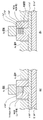
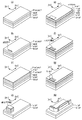
図3は、本発明の第1の実施形態による光集積回路の作製方法を説明するための図である。簡単のため、片方の半導体マッハツェンダ変調器のみを示している。InP基板の(100)面上に、DFBレーザが[011]方向に配置され、半導体マッハツェンダ変調器が[01−1]方向に配置され、両者が光導波路で接続されている。図4(a)は、図3のa−a線に沿ったDFBレーザの断面図であり、図4(b)は、図3のb−b線に沿った半導体マッハツェンダ変調器の断面図である。図5を参照して、作製方法の説明を行うが、当業者であれば前後の記載から容易に類推できるプロセスについては一部省略してある。
EXAMPLE FIG. 3 is a diagram for explaining a method of manufacturing an optical integrated circuit according to the first embodiment of the present invention. For simplicity, only one semiconductor Mach-Zehnder modulator is shown. On the (100) plane of the InP substrate, a DFB laser is arranged in the [011] direction, a semiconductor Mach-Zehnder modulator is arranged in the [01-1] direction, and both are connected by an optical waveguide. 4A is a cross-sectional view of the DFB laser along the line aa in FIG. 3, and FIG. 4B is a cross-sectional view of the semiconductor Mach-Zehnder modulator along the line bb in FIG. is there. The manufacturing method will be described with reference to FIGS. 5A and 5B, but some processes that can be easily inferred from the preceding and following descriptions by those skilled in the art are partially omitted.
まず、DFBレーザの作製方法を説明する。SI(semi−insulating)−InP基板の(100)面上にn型InPを成長し、その上に、PL波長1.15μmの無歪のInGaAlAsガイド層を成長する(図示せず)。その上に、多重量子井戸(multiple quantum well:MQW)構造を有する活性層を成長する。多重量子井戸構造は、PL波長1.55μm、+1.0%の圧縮歪で厚さ7nmのInGaAlAs井戸層と、PL波長1.20μm、−0.4%の引張歪で厚さ10nmのInGaAlAs障壁層とを8周期繰り返した構造である。この活性層上に、p−InGaAsP層を形成する(図5(a))。 First, a method for manufacturing a DFB laser will be described. An n-type InP is grown on a (100) plane of an SI (semi-insulating) -InP substrate, and an unstrained InGaAlAs guide layer having a PL wavelength of 1.15 μm is grown thereon (not shown). An active layer having a multiple quantum well (MQW) structure is grown thereon. The multi-quantum well structure has an InGaAlAs well layer with a PL wavelength of 1.55 μm and a compressive strain of + 1.0% and a thickness of 7 nm, and an InGaAlAs barrier with a PL wavelength of 1.20 μm and a tensile strain of −0.4% and a thickness of 10 nm. It is a structure in which a layer is repeated for 8 periods. A p-InGaAsP layer is formed on this active layer (FIG. 5A).
次に、リソグラフィとエッチングを用いてp−InGaAsP層に回折格子を形成する(図5(b))。回折格子の溝は、後述のプロセスでメサ構造を作製する[011]方向に垂直な方向、すなわち[01−1]方向に平行になるように作製する。 Next, a diffraction grating is formed in the p-InGaAsP layer using lithography and etching (FIG. 5B). The grooves of the diffraction grating are manufactured so as to be parallel to the [011] direction perpendicular to the [011] direction in which the mesa structure is manufactured by a process described later.
そして、p−InPオーバークラッド層、p−InGaAsPコンタクト層を順に結晶成長する(図5(c))。 Then, a p-InP overclad layer and a p-InGaAsP contact layer are grown in order (FIG. 5C).
ここまでの工程で、DFBレーザ部分の層構造が完成する。これを利用し、バットジョイント技術を用いてDFBレーザと結合した半導体マッハツェンダ変調器を作製していく。 The layer structure of the DFB laser portion is completed through the steps so far. Utilizing this, a semiconductor Mach-Zehnder modulator coupled with a DFB laser is manufactured using a butt joint technique.
最初に、図5(c)の層構造上にSiO2マスクを付け、標準的なフォトリソグラフィとエッチングを用いてパターニングする。パターニングは、回折格子を作りこんだ領域の直上に幅が15μm、長さが450μmの島状のパターンが残るように行う。ここで、長さ方向は、回折格子の溝が並ぶ方向であり、具体的には[011]方向である。次に、エッチングにより、MQWによる活性層まで除去し、幅が15μm、長さが450μmの島状のメサ構造を形成する(図5(d))。すなわち、幅15μm、長さ450μmの領域にのみ、MQWによる活性層を残した状態にする。なお、活性層とInP基板に挟まれたn-InP層はDFBレーザ部分と半導体マッハツェンダ変調器部分とで共有するため、島状メサ構造形成時に、エッチングにより誤って除去しないようにする。 Initially, a SiO2 mask is applied over the layer structure of FIG. 5C and patterned using standard photolithography and etching. The patterning is performed so that an island pattern having a width of 15 μm and a length of 450 μm remains immediately above the region where the diffraction grating is formed. Here, the length direction is the direction in which the grooves of the diffraction grating are arranged, specifically, the [011] direction. Next, the active layer by MQW is removed by etching to form an island-like mesa structure having a width of 15 μm and a length of 450 μm (FIG. 5D). In other words, the MQW active layer is left only in the region having a width of 15 μm and a length of 450 μm. The n-InP layer sandwiched between the active layer and the InP substrate is shared by the DFB laser portion and the semiconductor Mach-Zehnder modulator portion, so that it is not mistakenly removed by etching when the island mesa structure is formed.
次に、SiO2マスクを用いて選択成長することで、DFBレーザ部分を埋め込むように半導体マッハツェンダ変調器の層構造を結晶成長する(図5(e))。変調器部分として成長する構造は以下の通りである。最初に、厚さ0.4μmのn型GaAlAs/InAlAsからなる多重量子井戸活性層を成長させ、続けて厚さ0.5μmのi-InP、キャリアーブロック層となる厚さ0.05μm、ホール濃度1×1018のp-InP、n−InPオーバークラッド層、p−InGaAsコンタクト層を順に成長する。これにより、npin構造を有する変調器の層構造が形成されるのと同時に、DFBレーザ部分とバッドジョイントにより結合される。 Next, the layer structure of the semiconductor Mach-Zehnder modulator is crystal-grown so as to embed the DFB laser portion by selective growth using a SiO 2 mask (FIG. 5E). The structure that grows as the modulator portion is as follows. First, an n-type GaAlAs / InAlAs multi-quantum well active layer having a thickness of 0.4 μm is grown, followed by i-InP having a thickness of 0.5 μm, a thickness of 0.05 μm to be a carrier block layer, a hole concentration. A 1 × 10 18 p-InP, n-InP overclad layer, and p-InGaAs contact layer are grown in this order. Thereby, the layer structure of the modulator having the npin structure is formed, and at the same time, it is coupled to the DFB laser portion by the bad joint.
次に、DFBレーザ部分のSiO2マスクをフッ酸で除去した後、再度SiO2を堆積し、フォトリソグラフィとエッチングによりDFBレーザ部分の一部にストライプ状の開口部を2つ持ったマスクを新しく形成する。これをマスクにして反応性イオンエッチング(Reactive Ion Etching:RIE)によりDFBレーザ部分の活性層まで除去する。これにより、幅2μmのハイメサ構造を形成する(図5(f))。ハイメサ構造は、次の電流ブロック層の再成長が行いやすいように、[011]方向に平行な方向きに形成する。 Next, after removing the SiO2 mask in the DFB laser portion with hydrofluoric acid, SiO2 is deposited again, and a mask having two stripe-shaped openings in a part of the DFB laser portion is formed by photolithography and etching. . Using this as a mask, the active layer of the DFB laser portion is removed by reactive ion etching (RIE). As a result, a high mesa structure with a width of 2 μm is formed (FIG. 5F). The high mesa structure is formed in a direction parallel to the [011] direction so that the next current block layer can be easily regrown.
次いで、ハイメサ構造の両側面に、先にエッチングした量に匹敵する厚さ分だけ、FeドープのInP層を結晶成長する(図5(g))。このInP層は、DFBレーザに対する電流ブロック層として機能する。 Next, an Fe-doped InP layer is grown on both sides of the high mesa structure by a thickness equivalent to the amount etched previously (FIG. 5G). This InP layer functions as a current blocking layer for the DFB laser.
次に、先ほど用いたSiO2マスクをフッ酸により除去し、再度、SiO2を成膜する。フォトリソグラフィとエッチングにより、DFBレーザと半導体マッハツェンダ変調器を形成する部分をマスクした後、RIE法によりDFBレーザと半導体マッハツェンダ変調器の形状のハイメサ導波路を残してInP基板直上のn―InPが露出するまでエッチングする(図5(h))。半導体マッハツェンダ変調器は、一般のマッハツェンダ変調器と同様に、入力側の分波器と、分波器により分波された光信号に対して位相変調を行うための2本のアーム導波路と、2本のアーム導波路に接続された合波器とを備えるが、上記半導体マッハツェンダ変調器の両アーム導波路は、ポッケルス効果を最大化するために[01−1]方向に平行となるように形成する。ここまでの工程で、DFBレーザと半導体マッハツェンダ変調器の構造が形成される。 Next, the SiO2 mask used previously is removed with hydrofluoric acid, and SiO2 is formed again. After masking the portion where the DFB laser and the semiconductor Mach-Zehnder modulator are formed by photolithography and etching, the n-InP is exposed immediately above the InP substrate leaving the high mesa waveguide in the shape of the DFB laser and the semiconductor Mach-Zehnder modulator by the RIE method. Etching is performed until this is done (FIG. 5 (h)). The semiconductor Mach-Zehnder modulator, like a general Mach-Zehnder modulator, includes an input-side duplexer, two arm waveguides for performing phase modulation on the optical signal demultiplexed by the duplexer, A multiplexer connected to two arm waveguides, and both arm waveguides of the semiconductor Mach-Zehnder modulator are parallel to the [01-1] direction in order to maximize the Pockels effect. Form. Through the steps so far, the structure of the DFB laser and the semiconductor Mach-Zehnder modulator is formed.
その後、半導体マッハツェンダ変調器の両アーム導波路間およびDFBレーザ・半導体マッハツェンダ変調器間の電気的な絶縁を行うために、分離溝を形成して各部でn−InPコンタクト層が独立するようにする。次いで、DFBレーザの上面にp電極を、DFBレーザ及びマッハツェンダ変調器のn-InPコンタクト層上にn電極を形成した。そして、ポリイミド、BCB等の絶縁性有機膜を全面に塗布し、半導体マッハツェンダ変調器のメサ脇のみを残して有機膜を除去する。各種電極を形成し、その後、SI−InP基板を研磨した後にへき開を行う。 Thereafter, in order to electrically insulate between the arm waveguides of the semiconductor Mach-Zehnder modulator and between the DFB laser and the semiconductor Mach-Zehnder modulator, an isolation groove is formed so that the n-InP contact layer is independent in each part. . Next, a p-electrode was formed on the upper surface of the DFB laser, and an n-electrode was formed on the n-InP contact layers of the DFB laser and the Mach-Zehnder modulator. Then, an insulating organic film such as polyimide or BCB is applied to the entire surface, and the organic film is removed leaving only the mesa side of the semiconductor Mach-Zehnder modulator. Various electrodes are formed, and then cleavage is performed after the SI-InP substrate is polished.
本実施例の説明にあたり、各種の材料や加工技術に言及したが、これらは、本発明の第1の実施形態による光集積回路の作製方法を十分に説明するためのものであり、本発明に係る光集積回路をこれらの材料や加工技術により作製されたものに限定する意図ではない。たとえば、半導体基板としてInP基板を例に説明したが、閃亜鉛鉱型(ジンクブレンド型)構造の半導体基板を用いることができる。 In the description of this example, various materials and processing techniques were mentioned, but these are for fully explaining the method of manufacturing the optical integrated circuit according to the first embodiment of the present invention. The optical integrated circuit is not intended to be limited to those manufactured by these materials and processing techniques. For example, although an InP substrate has been described as an example of a semiconductor substrate, a semiconductor substrate having a zinc blende type (zinc blend type) structure can be used.
このように作製した本実施例の光集積回路により、3dBmの光出力と、3dB帯域30GHzの高速変調特性が得られることが確認された。これは、本実施例の構成により、高速変調器が実現できていることを示している。 It was confirmed that a 3 dBm optical output and a high-speed modulation characteristic with a 3 dB bandwidth of 30 GHz can be obtained by the optical integrated circuit of this example manufactured in this way. This indicates that a high-speed modulator can be realized by the configuration of this embodiment.
(第2の実施形態)
第1の実施形態の双方向光出力の波長可変DFBレーザアレイを集積した半導体マッハツェンダ変調器では、2つの12×1のMMI型合波器を介して、双方向出力されていた。第2の実施形態は、この部分から、後段に続くDQPSKのカップラーの一部を、N×Mのファネル導波路に置き換える。
(Second Embodiment)
In the semiconductor Mach-Zehnder modulator in which the tunable DFB laser array with bidirectional optical output of the first embodiment is integrated, bidirectional output is performed via two 12 × 1 MMI type multiplexers. The second embodiment replaces a part of the DQPSK coupler following the latter part with an N × M funnel waveguide from this part.
図6は、図2のうち、第2の実施形態において置き換える部分を点線で示した図である。この場合は、Nは12、Mは4となる。第1の実施形態の構成では、双方向光出力の波長可変DFBレーザアレイの双方の出力で、12本のDFBレーザが12×1のMMI型合波器を通過した後、2等分され、さらにそれぞれが2等分される。駆動しているDFBレーザの光強度は、このMMI型合波器を通過することで、1/12になり、その後、SOAを通過し、ゲインを得る。さらに、続く2段のカップラーを通過することで4本のアーム導波路に分配されることになり、双方向で同じことが起こる。この構成は、ある意味で一度光を減衰させてから増幅するという形となっている。減衰が小さくできれば、無論増幅が小さくても良く、エネルギー消費が抑えられる。また、十分な光強度が得られるのであればSOAが不要となる。加えてSOAがいらない場合は、プロセスの簡略化ができ、製造コスト低減が可能となる。 FIG. 6 is a diagram showing a part to be replaced in the second embodiment in FIG. 2 by a dotted line. In this case, N is 12 and M is 4. In the configuration of the first embodiment, 12 DFB lasers are divided into two equal parts after passing through a 12 × 1 MMI type multiplexer at both outputs of the tunable DFB laser array with bidirectional optical output, Each is further divided into two equal parts. The light intensity of the driving DFB laser becomes 1/12 by passing through this MMI type multiplexer, and then passes through the SOA to obtain a gain. Furthermore, when passing through the subsequent two-stage coupler, it is distributed to the four arm waveguides, and the same thing occurs in both directions. In this sense, this configuration is such that light is attenuated and then amplified. Of course, if the attenuation can be reduced, the amplification may be small and energy consumption can be suppressed. Further, if sufficient light intensity can be obtained, SOA is not necessary. In addition, when SOA is not required, the process can be simplified and the manufacturing cost can be reduced.
そこで、この部分を12×4のファネル合波器に置き換える。どちらにせよ4つに配分するので、図中点線で囲まれる箇所(図中では説明を簡潔にするため上部分だけ示しているが、下側の対称な個所も同じである。)を、12×4のファネル合波器に置き換えれば、無駄に減衰させる割合が減少でき、1/12に減衰させられていたのを、4/12、つまり1/3までの減衰で済むようにできるようになり、双方向光出力の利用に加えて、さらにエネルギーの利用効率を高めることが可能となる。 Therefore, this part is replaced with a 12 × 4 funnel multiplexer. In any case, since it is divided into four parts, the part surrounded by a dotted line in the figure (only the upper part is shown in the figure for the sake of brevity, but the lower symmetrical part is also the same). If it is replaced with a × 4 funnel multiplexer, the rate of unnecessary attenuation can be reduced, and the attenuation of 1/12 can be reduced to 4/12, that is, 1/3. Thus, in addition to the use of bidirectional light output, it is possible to further increase the energy utilization efficiency.
ここで、12×4のファネル合波器を本実施形態では利用したが、12×4のMMIを利用しても同様の効果が得られる。また、本実施形態では波長可変DFBレーザアレイを光源として用いているが、活性部がアレイを構成し、かつ、合波器を介して出力され、さらに双方向出力を利用できる波長可変であれば無論同じ効果が得られる。 Here, although a 12 × 4 funnel multiplexer is used in the present embodiment, the same effect can be obtained even if a 12 × 4 MMI is used. In this embodiment, the wavelength tunable DFB laser array is used as a light source. However, if the active portion constitutes the array, is output through a multiplexer, and is tunable so that bidirectional output can be used. Of course, the same effect can be obtained.
(第3の実施形態)
第1の実施形態では、半導体マッハツェンダ変調器を通過した後、片方の偏波をTEモードからTMモードに変換した後、PBCを通過することにより他方のDQPSK光変調器の出力(TE)と合波される。集積デバイスでは、集積される要素デバイスの完成度、歩留りが高くなければ、デバイス全体で、性能を引き出せない、歩留りが著しく低くなるという問題がある。特に、第1の実施形態の中で半導体からなる偏波ローテーターは、製造が難しい。
(Third embodiment)
In the first embodiment, after passing through the semiconductor Mach-Zehnder modulator, one polarization is converted from the TE mode to the TM mode, and then passed through the PBC to match the output (TE) of the other DQPSK optical modulator. Waved. In an integrated device, there is a problem that unless the completeness and yield of the element devices to be integrated are high, the performance of the entire device cannot be obtained, and the yield is remarkably reduced. In particular, the polarization rotator made of a semiconductor in the first embodiment is difficult to manufacture.
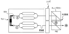
そこで、本実施形態では、図6の点線より右の部分を、空間系のバルクマイクロ工学系を利用して構成する。 Therefore, in the present embodiment, the portion to the right of the dotted line in FIG. 6 is configured using a space-based bulk microengineering system.
図7に、本実施形態に係る光集積回路を示す。それぞれの単一モード半導体波長可変レーザの双方向出力から出たTE偏向の光が、半導体マッハツェンダ変調器を通過した後、レンズを通過することでコリメートされる。一方は、レンズを介してキューブミラーと光学的に結合し、キューブミラーを通過して光路を90度変換する。その後、キューブミラーの一面に張り合わされた半波長板を通過し、TM偏向に偏波を回転させる。その後、半波長板と、キューブミラーと対向する面で張り合わされたPBCを通過して、合波され出力される。実際は、図示していないが、アイソレーターを通過し再度レンズでファイバーにフォーカスされ出力される。本実施形態の例では1mm角のキューブミラー、PBCを利用し、ポリイミドからなる半波長板厚さ20μmを利用した。 FIG. 7 shows an optical integrated circuit according to this embodiment. The TE-polarized light emitted from the bidirectional output of each single-mode semiconductor wavelength tunable laser is collimated by passing through the lens after passing through the semiconductor Mach-Zehnder modulator. One is optically coupled to the cube mirror through a lens and passes through the cube mirror to change the optical path by 90 degrees. Thereafter, the light passes through a half-wave plate attached to one surface of the cube mirror, and the polarization is rotated by TM deflection. Thereafter, the light passes through the half-wave plate and the PBC bonded on the surface facing the cube mirror, and is combined and output. Actually, though not shown, the light passes through the isolator and is again focused on the fiber by the lens and output. In the example of this embodiment, a 1 mm square cube mirror and PBC are used, and a half-wave plate thickness of 20 μm made of polyimide is used.
本構成では、半導体チップを出てから、ふたつのブロックに挟まれた半波長板を通過する。図中上方の光経路は、下方を経由してくる光よりも光路長が長い。つまり偏波により大きく送信タイミングがずれることになる。スキュー(偏波間の送信タイミングのずれ)を解消するために、短い光路となる方の導波路に遅延線を設けてスキューを解消する構造としてある。遅延線の長さは、導波路の屈折率と、構成するキューブミラー、半波長板の屈折率厚さにより遅延量を適時決定すればよい。 In this configuration, after leaving the semiconductor chip, it passes through a half-wave plate sandwiched between two blocks. The upper optical path in the figure has a longer optical path length than the light passing through the lower part. That is, the transmission timing is greatly shifted due to the polarization. In order to eliminate skew (transmission timing deviation between polarized waves), a delay line is provided in the waveguide that becomes the short optical path to eliminate the skew. The length of the delay line may be determined in a timely manner by the refractive index of the waveguide and the refractive index thickness of the cube mirror and the half-wave plate constituting the waveguide.
また、必ずしもこの遅延線は必要ではなく、光変調に用いる高速電気信号を遅延することによってもスキューを回避することはできる。 Further, this delay line is not necessarily required, and skew can be avoided by delaying a high-speed electrical signal used for optical modulation.
本実施例によると、空間系部材と組み合わせることで、双方向出力を利用した低消費電力のDP-QPSKを歩留り良く作製できる。 According to this embodiment, a low power consumption DP-QPSK using bidirectional output can be manufactured with a high yield by combining with a space system member.
Claims (9)
メサ構造を有する半導体レーザと、
前記半導体レーザの一端と第1の光導波路で接続された第1の半導体マッハツェンダ変調器であって、入力側の分波器と、前記分波器により分波された光信号に対して位相変調を行うための2本のアーム導波路と、前記2本のアーム導波路に接続された合波器とを有する第1の半導体マッハツェンダ変調器と、
前記半導体レーザの他端と第2の光導波路で接続された第2の半導体マッハツェンダ変調器であって、入力側の分波器と、前記分波器により分波された光信号に対して位相変調を行うための2本のアーム導波路と、前記2本のアーム導波路に接続された合波器とを有する第2の半導体マッハツェンダ変調器と
を備え、
前記半導体レーザの前記メサ構造の配置方向が、前記メサ構造の側面への再成長に最適な方向であり、
前記第1及び第2の半導体マッハツェンダ型変調器が有する前記2本のアーム導波路の活性層が多重量子井戸構造であり、
前記第1及び第2の半導体マッハツェンダ型変調器が有する前記2本のアーム導波路の配置方向が、前記2本のアーム導波路に光変調のための電界を印加したときに、ポッケルス効果による屈折率変化が量子閉じ込めシュタルク効果による屈折率変化を強める方向であることを特徴とする光集積回路。 In an optical integrated circuit in which a semiconductor laser and a semiconductor Mach-Zehnder type modulator are integrated on a zincblende type semiconductor substrate,
A semiconductor laser having a mesa structure;
A first semiconductor Mach-Zehnder modulator connected to one end of the semiconductor laser by a first optical waveguide, the phase splitter for an input-side duplexer and an optical signal demultiplexed by the duplexer A first semiconductor Mach-Zehnder modulator having two arm waveguides for performing the above and a multiplexer connected to the two arm waveguides;
A second semiconductor Mach-Zehnder modulator connected to the other end of the semiconductor laser by a second optical waveguide, the phase difference with respect to an input-side demultiplexer and an optical signal demultiplexed by the demultiplexer A second semiconductor Mach-Zehnder modulator having two arm waveguides for performing modulation and a multiplexer connected to the two arm waveguides;
The arrangement direction of the mesa structure of the semiconductor laser is an optimum direction for regrowth on the side surface of the mesa structure,
The active layers of the two arm waveguides of the first and second semiconductor Mach-Zehnder modulators have a multiple quantum well structure,
Refraction due to Pockels effect when the arrangement direction of the two arm waveguides of the first and second semiconductor Mach-Zehnder type modulators applies an electric field for optical modulation to the two arm waveguides. An optical integrated circuit characterized in that the rate change is in a direction to increase the change in refractive index due to the quantum confined Stark effect.
前記半導体レーザ及び前記半導体マッハツェンダ変調器は、前記InP基板の(100)面上に集積され、
前記半導体レーザの前記メサ構造の配置方向が、前記InP基板の[011]方向であり、前記マッハツェンダ型変調器が有する前記2本のアーム導波路の配置方向が、前記InP基板の[01−1]方向であることを特徴とする請求項1に記載の光集積回路。 The semiconductor substrate is an InP substrate;
The semiconductor laser and the semiconductor Mach-Zehnder modulator are integrated on the (100) surface of the InP substrate,
The arrangement direction of the mesa structure of the semiconductor laser is the [011] direction of the InP substrate, and the arrangement direction of the two arm waveguides of the Mach-Zehnder modulator is [01-1] of the InP substrate. The optical integrated circuit according to claim 1, wherein
前記DFBレーザの中央にλ/4シフトが配置されて、前記DFBレーザの両端からの光出力が等しいことを特徴とする請求項1又は2に記載の光集積回路。 The semiconductor laser is a DFB laser,
3. The optical integrated circuit according to claim 1, wherein a λ / 4 shift is arranged in the center of the DFB laser, and the optical outputs from both ends of the DFB laser are equal. 4.
前記波長可変DFBレーザアレイの中央にλ/4シフトが配置されて、前記波長可変DFBレーザアレイの両端からの光出力が等しいことを特徴とする請求項1又は2に記載の光集積回路。 The semiconductor laser is a wavelength tunable DFB laser array,
3. The optical integrated circuit according to claim 1, wherein a λ / 4 shift is arranged in the center of the wavelength tunable DFB laser array, and optical outputs from both ends of the wavelength tunable DFB laser array are equal.
前記キューブミラーの一面に張り合わされた半波長板と、
前記半波長板と、前記キューブミラーと対向する面で張り合わされた偏波合波器と
をさらに備え、
前記第1の半導体マッハツェンダ変調器から出力される光信号は、前記キューブミラーで前記半波長板の方向に光路が90度変換されて、前記半波長板を通過して前記偏波合波器に導入され、前記第2の半導体マッハツェンダ変調器から出力される光信号と、前記偏波合波器内で合波されることを特徴とする請求項1から5のいずれかに記載の光集積回路。 A cube mirror optically coupled to the output of the first semiconductor Mach-Zehnder modulator via a lens;
A half-wave plate attached to one surface of the cube mirror;
The half-wave plate and a polarization multiplexer bonded together on a surface facing the cube mirror,
The optical signal output from the first semiconductor Mach-Zehnder modulator is converted by the cube mirror in the direction of the half-wave plate by 90 degrees, passes through the half-wave plate, and enters the polarization multiplexer. The optical integrated circuit according to claim 1, wherein the optical integrated circuit is combined with an optical signal introduced and output from the second semiconductor Mach-Zehnder modulator in the polarization multiplexer. .
Priority Applications (1)
| Application Number | Priority Date | Filing Date | Title |
|---|---|---|---|
| JP2011014531A JP5542071B2 (en) | 2011-01-26 | 2011-01-26 | Optical integrated circuit |
Applications Claiming Priority (1)
| Application Number | Priority Date | Filing Date | Title |
|---|---|---|---|
| JP2011014531A JP5542071B2 (en) | 2011-01-26 | 2011-01-26 | Optical integrated circuit |
Publications (2)
| Publication Number | Publication Date |
|---|---|
| JP2012156336A true JP2012156336A (en) | 2012-08-16 |
| JP5542071B2 JP5542071B2 (en) | 2014-07-09 |
Family
ID=46837746
Family Applications (1)
| Application Number | Title | Priority Date | Filing Date |
|---|---|---|---|
| JP2011014531A Active JP5542071B2 (en) | 2011-01-26 | 2011-01-26 | Optical integrated circuit |
Country Status (1)
| Country | Link |
|---|---|
| JP (1) | JP5542071B2 (en) |
Cited By (16)
| Publication number | Priority date | Publication date | Assignee | Title |
|---|---|---|---|---|
| JP2014081578A (en) * | 2012-10-18 | 2014-05-08 | Nippon Telegr & Teleph Corp <Ntt> | Optical transmission device |
| JP2014119468A (en) * | 2012-12-13 | 2014-06-30 | Mitsubishi Electric Corp | Wavelength variable light source |
| WO2014107537A1 (en) | 2013-01-02 | 2014-07-10 | Packet Photonics, Inc. | Tunable u-laser transmitter with integrated mach-zehnder modulator |
| WO2014119450A1 (en) * | 2013-01-31 | 2014-08-07 | 住友大阪セメント株式会社 | Optical modulator |
| JP2014186127A (en) * | 2013-03-22 | 2014-10-02 | Nippon Telegr & Teleph Corp <Ntt> | Polarization combiner, and optical modulator having the same |
| JP2015011069A (en) * | 2013-06-26 | 2015-01-19 | 日本電信電話株式会社 | Polarization beam combiner |
| JP2015095513A (en) * | 2013-11-11 | 2015-05-18 | 日本電信電話株式会社 | Wavelength variable light source |
| JP2015122352A (en) * | 2013-12-20 | 2015-07-02 | 三菱電機株式会社 | Wavelength variable light source, wavelength variable light source module, and optical integrated element |
| JPWO2014051096A1 (en) * | 2012-09-28 | 2016-08-25 | 住友大阪セメント株式会社 | Optical modulator and optical modulation method |
| US9448585B2 (en) | 2014-02-26 | 2016-09-20 | Wistron Corporation | Clamping structure, electronic device and clamping component |
| JP2017528769A (en) * | 2014-09-17 | 2017-09-28 | 華為技術有限公司Huawei Technologies Co.,Ltd. | Optical signal modulation apparatus and system |
| JP2017207587A (en) * | 2016-05-17 | 2017-11-24 | 日本電信電話株式会社 | Semiconductor optical modulator and method for forming the same |
| US9887780B2 (en) | 2009-05-28 | 2018-02-06 | Freedom Photonics, Llc. | Chip-based advanced modulation format transmitter |
| US9941971B1 (en) | 2013-07-23 | 2018-04-10 | Freedom Photonics, Llc. | Integrated interferometric optical transmitter |
| CN113872698A (en) * | 2020-06-30 | 2021-12-31 | 慧与发展有限责任合伙企业 | Low driving voltage multi-wavelength transmitter |
| US11251584B2 (en) | 2017-03-28 | 2022-02-15 | Freedom Photonics Llc | Tunable laser |
Citations (14)
| Publication number | Priority date | Publication date | Assignee | Title |
|---|---|---|---|---|
| JPH02130517A (en) * | 1988-11-11 | 1990-05-18 | Fujitsu Ltd | Polarized wave coupler |
| JPH03291523A (en) * | 1990-04-09 | 1991-12-20 | Nippon Telegr & Teleph Corp <Ntt> | Encoder |
| JPH06260727A (en) * | 1993-01-07 | 1994-09-16 | Nec Corp | Optical semiconductor device and manufacture thereof |
| JPH08334796A (en) * | 1995-06-07 | 1996-12-17 | Oki Electric Ind Co Ltd | Optical wavelength conversion integrating element |
| JPH1090542A (en) * | 1996-09-17 | 1998-04-10 | Nippon Telegr & Teleph Corp <Ntt> | Bury-in semiconductor optical device |
| JPH11307856A (en) * | 1998-04-21 | 1999-11-05 | Toshiba Corp | Distributed feedback laser and manufacture thereof |
| JP2001196626A (en) * | 2000-01-06 | 2001-07-19 | Nippon Telegr & Teleph Corp <Ntt> | Apparatus for optical interconnection of wiring boards |
| JP2002040504A (en) * | 2000-07-07 | 2002-02-06 | Lucent Technol Inc | Wavelength converter |
| JP2002169131A (en) * | 2000-12-04 | 2002-06-14 | Fujitsu Ltd | Optical semiconductor device, and modulation method of the optical semiconductor device |
| JP2004111709A (en) * | 2002-09-19 | 2004-04-08 | Mitsubishi Electric Corp | Semiconductor laser |
| JP2007065357A (en) * | 2005-08-31 | 2007-03-15 | Furukawa Electric Co Ltd:The | Multimode interference coupler, optical semiconductor element using the same, and method for designing the multimode interference coupler |
| JP2009049613A (en) * | 2007-08-16 | 2009-03-05 | Fujitsu Ltd | Coherent light receiver and optical communication system |
| JP2010081287A (en) * | 2008-09-26 | 2010-04-08 | Fujitsu Ltd | Optical signal transmitting device |
| JP2010113084A (en) * | 2008-11-05 | 2010-05-20 | Nippon Telegr & Teleph Corp <Ntt> | Optical signal processing device |
-
2011
- 2011-01-26 JP JP2011014531A patent/JP5542071B2/en active Active
Patent Citations (14)
| Publication number | Priority date | Publication date | Assignee | Title |
|---|---|---|---|---|
| JPH02130517A (en) * | 1988-11-11 | 1990-05-18 | Fujitsu Ltd | Polarized wave coupler |
| JPH03291523A (en) * | 1990-04-09 | 1991-12-20 | Nippon Telegr & Teleph Corp <Ntt> | Encoder |
| JPH06260727A (en) * | 1993-01-07 | 1994-09-16 | Nec Corp | Optical semiconductor device and manufacture thereof |
| JPH08334796A (en) * | 1995-06-07 | 1996-12-17 | Oki Electric Ind Co Ltd | Optical wavelength conversion integrating element |
| JPH1090542A (en) * | 1996-09-17 | 1998-04-10 | Nippon Telegr & Teleph Corp <Ntt> | Bury-in semiconductor optical device |
| JPH11307856A (en) * | 1998-04-21 | 1999-11-05 | Toshiba Corp | Distributed feedback laser and manufacture thereof |
| JP2001196626A (en) * | 2000-01-06 | 2001-07-19 | Nippon Telegr & Teleph Corp <Ntt> | Apparatus for optical interconnection of wiring boards |
| JP2002040504A (en) * | 2000-07-07 | 2002-02-06 | Lucent Technol Inc | Wavelength converter |
| JP2002169131A (en) * | 2000-12-04 | 2002-06-14 | Fujitsu Ltd | Optical semiconductor device, and modulation method of the optical semiconductor device |
| JP2004111709A (en) * | 2002-09-19 | 2004-04-08 | Mitsubishi Electric Corp | Semiconductor laser |
| JP2007065357A (en) * | 2005-08-31 | 2007-03-15 | Furukawa Electric Co Ltd:The | Multimode interference coupler, optical semiconductor element using the same, and method for designing the multimode interference coupler |
| JP2009049613A (en) * | 2007-08-16 | 2009-03-05 | Fujitsu Ltd | Coherent light receiver and optical communication system |
| JP2010081287A (en) * | 2008-09-26 | 2010-04-08 | Fujitsu Ltd | Optical signal transmitting device |
| JP2010113084A (en) * | 2008-11-05 | 2010-05-20 | Nippon Telegr & Teleph Corp <Ntt> | Optical signal processing device |
Cited By (28)
| Publication number | Priority date | Publication date | Assignee | Title |
|---|---|---|---|---|
| US9887780B2 (en) | 2009-05-28 | 2018-02-06 | Freedom Photonics, Llc. | Chip-based advanced modulation format transmitter |
| JPWO2014051096A1 (en) * | 2012-09-28 | 2016-08-25 | 住友大阪セメント株式会社 | Optical modulator and optical modulation method |
| JP2014081578A (en) * | 2012-10-18 | 2014-05-08 | Nippon Telegr & Teleph Corp <Ntt> | Optical transmission device |
| JP2014119468A (en) * | 2012-12-13 | 2014-06-30 | Mitsubishi Electric Corp | Wavelength variable light source |
| JP2016509370A (en) * | 2013-01-02 | 2016-03-24 | オーイー・ソリューションズ・アメリカ・インコーポレーテッド | Tunable U laser transmitter with integrated Mach-Zehnder modulator |
| CN105409070A (en) * | 2013-01-02 | 2016-03-16 | Oe解决方案美国股份有限公司 | Tunable U-laser transmitter with integrated Mach-Zehnder modulator |
| US9755753B2 (en) | 2013-01-02 | 2017-09-05 | Oe Solutions America, Inc. | Tunable U-laser transmitter with integrated Mach-Zehnder Modulator |
| KR102162833B1 (en) * | 2013-01-02 | 2020-10-08 | 오이솔루션 아메리카 인코퍼레이티드 | Tunable u-laser transmitter with integrated mach-zehnder modulator |
| CN105409070B (en) * | 2013-01-02 | 2019-08-16 | Oe解决方案美国股份有限公司 | Adjustable U laser emitter with integrated Mach-Zehnder modulators |
| WO2014107537A1 (en) | 2013-01-02 | 2014-07-10 | Packet Photonics, Inc. | Tunable u-laser transmitter with integrated mach-zehnder modulator |
| KR20150122642A (en) * | 2013-01-02 | 2015-11-02 | 오이솔루션 아메리카 인코퍼레이티드 | Tunable u-laser transmitter with integrated mach-zehnder modulator |
| EP2941802A4 (en) * | 2013-01-02 | 2016-08-31 | Oe Solutions America Inc | Tunable u-laser transmitter with integrated mach-zehnder modulator |
| JP2014149398A (en) * | 2013-01-31 | 2014-08-21 | Sumitomo Osaka Cement Co Ltd | Optical modulator |
| WO2014119450A1 (en) * | 2013-01-31 | 2014-08-07 | 住友大阪セメント株式会社 | Optical modulator |
| CN104981727A (en) * | 2013-01-31 | 2015-10-14 | 住友大阪水泥股份有限公司 | Optical modulator |
| US9703169B2 (en) | 2013-01-31 | 2017-07-11 | Sumitomo Osaka Cement Co., Ltd. | Optical modulator |
| JP2014186127A (en) * | 2013-03-22 | 2014-10-02 | Nippon Telegr & Teleph Corp <Ntt> | Polarization combiner, and optical modulator having the same |
| JP2015011069A (en) * | 2013-06-26 | 2015-01-19 | 日本電信電話株式会社 | Polarization beam combiner |
| US9941971B1 (en) | 2013-07-23 | 2018-04-10 | Freedom Photonics, Llc. | Integrated interferometric optical transmitter |
| JP2015095513A (en) * | 2013-11-11 | 2015-05-18 | 日本電信電話株式会社 | Wavelength variable light source |
| JP2015122352A (en) * | 2013-12-20 | 2015-07-02 | 三菱電機株式会社 | Wavelength variable light source, wavelength variable light source module, and optical integrated element |
| US9448585B2 (en) | 2014-02-26 | 2016-09-20 | Wistron Corporation | Clamping structure, electronic device and clamping component |
| JP2017528769A (en) * | 2014-09-17 | 2017-09-28 | 華為技術有限公司Huawei Technologies Co.,Ltd. | Optical signal modulation apparatus and system |
| US10027417B2 (en) | 2014-09-17 | 2018-07-17 | Huawei Technologies Co., Ltd. | Optical signal modulation apparatus and system |
| JP2017207587A (en) * | 2016-05-17 | 2017-11-24 | 日本電信電話株式会社 | Semiconductor optical modulator and method for forming the same |
| US11251584B2 (en) | 2017-03-28 | 2022-02-15 | Freedom Photonics Llc | Tunable laser |
| CN113872698A (en) * | 2020-06-30 | 2021-12-31 | 慧与发展有限责任合伙企业 | Low driving voltage multi-wavelength transmitter |
| CN113872698B (en) * | 2020-06-30 | 2023-05-23 | 慧与发展有限责任合伙企业 | Low-driving-voltage multi-wavelength emitter and optical system |
Also Published As
| Publication number | Publication date |
|---|---|
| JP5542071B2 (en) | 2014-07-09 |
Similar Documents
| Publication | Publication Date | Title |
|---|---|---|
| JP5542071B2 (en) | Optical integrated circuit | |
| Coldren et al. | High performance InP-based photonic ICs—A tutorial | |
| US8718486B2 (en) | Chip-based advanced modulation format transmitter | |
| CN110168824B (en) | Semiconductor optical amplifier, method for manufacturing the same, and optical phase modulator | |
| JP2017098362A (en) | Optical integrated device and optical communication device | |
| WO2017135381A1 (en) | Optical transmitter and light intensity monitoring method | |
| US9728938B2 (en) | Optical semiconductor device, optical semiconductor device array, and optical transmitter module | |
| JP5545847B2 (en) | Optical semiconductor device | |
| JP2004281656A (en) | Gain-clamped semiconductor light amplifier | |
| de Valicourt et al. | Photonic integrated circuit based on hybrid III–V/silicon integration | |
| Ohyama et al. | Compact hybrid integrated 100-Gb/s transmitter optical sub-assembly using optical butt-coupling between EADFB lasers and silica-based AWG multiplexer | |
| Kono et al. | Compact and low power DP-QPSK modulator module with InP-based modulator and driver ICs | |
| Hatta et al. | Polarization-insensitive monolithic 40-Gbps SOA–MZI wavelength converter with narrow active waveguides | |
| JP2015094812A (en) | Wavelength variable light source | |
| JP6320192B2 (en) | Wavelength variable light source and wavelength variable light source module | |
| JP2015138847A (en) | Wavelength multiplex transmitter | |
| Andriolli et al. | Monolithically integrated all-optical regenerator for constant envelope WDM signals | |
| Fujisawa et al. | 1.3-µm, 50-Gbit/s EADFB lasers for 400GbE | |
| JP2015122352A (en) | Wavelength variable light source, wavelength variable light source module, and optical integrated element | |
| US11804905B1 (en) | Optical full-field transmitter | |
| Tsuzuki et al. | Full C-band tunable DFB laser array copackaged with InP Mach–Zehnder modulator for DWDM optical communication systems | |
| JP6557631B2 (en) | Optical transmitter | |
| JP2014191218A (en) | Optical modulator | |
| JP2019079993A (en) | Semiconductor optical element | |
| JP3246703B2 (en) | Semiconductor laser capable of polarization modulation and optical communication system using the same |
Legal Events
| Date | Code | Title | Description |
|---|---|---|---|
| A621 | Written request for application examination |
Free format text: JAPANESE INTERMEDIATE CODE: A621 Effective date: 20130208 |
|
| A977 | Report on retrieval |
Free format text: JAPANESE INTERMEDIATE CODE: A971007 Effective date: 20131120 |
|
| A131 | Notification of reasons for refusal |
Free format text: JAPANESE INTERMEDIATE CODE: A131 Effective date: 20131210 |
|
| A521 | Written amendment |
Free format text: JAPANESE INTERMEDIATE CODE: A523 Effective date: 20140207 |
|
| TRDD | Decision of grant or rejection written | ||
| A01 | Written decision to grant a patent or to grant a registration (utility model) |
Free format text: JAPANESE INTERMEDIATE CODE: A01 Effective date: 20140430 |
|
| A61 | First payment of annual fees (during grant procedure) |
Free format text: JAPANESE INTERMEDIATE CODE: A61 Effective date: 20140502 |
|
| R150 | Certificate of patent or registration of utility model |
Ref document number: 5542071 Country of ref document: JP Free format text: JAPANESE INTERMEDIATE CODE: R150 |