JP2012146853A - Method of manufacturing semiconductor device - Google Patents
Method of manufacturing semiconductor device Download PDFInfo
- Publication number
- JP2012146853A JP2012146853A JP2011004758A JP2011004758A JP2012146853A JP 2012146853 A JP2012146853 A JP 2012146853A JP 2011004758 A JP2011004758 A JP 2011004758A JP 2011004758 A JP2011004758 A JP 2011004758A JP 2012146853 A JP2012146853 A JP 2012146853A
- Authority
- JP
- Japan
- Prior art keywords
- wiring board
- chip
- mother
- carrier substrate
- semiconductor
- Prior art date
- Legal status (The legal status is an assumption and is not a legal conclusion. Google has not performed a legal analysis and makes no representation as to the accuracy of the status listed.)
- Withdrawn
Links
Images


Classifications
-
- H—ELECTRICITY
- H01—ELECTRIC ELEMENTS
- H01L—SEMICONDUCTOR DEVICES NOT COVERED BY CLASS H10
- H01L24/00—Arrangements for connecting or disconnecting semiconductor or solid-state bodies; Methods or apparatus related thereto
- H01L24/93—Batch processes
- H01L24/95—Batch processes at chip-level, i.e. with connecting carried out on a plurality of singulated devices, i.e. on diced chips
- H01L24/97—Batch processes at chip-level, i.e. with connecting carried out on a plurality of singulated devices, i.e. on diced chips the devices being connected to a common substrate, e.g. interposer, said common substrate being separable into individual assemblies after connecting
-
- H—ELECTRICITY
- H01—ELECTRIC ELEMENTS
- H01L—SEMICONDUCTOR DEVICES NOT COVERED BY CLASS H10
- H01L23/00—Details of semiconductor or other solid state devices
- H01L23/28—Encapsulations, e.g. encapsulating layers, coatings, e.g. for protection
- H01L23/31—Encapsulations, e.g. encapsulating layers, coatings, e.g. for protection characterised by the arrangement or shape
- H01L23/3107—Encapsulations, e.g. encapsulating layers, coatings, e.g. for protection characterised by the arrangement or shape the device being completely enclosed
- H01L23/3135—Double encapsulation or coating and encapsulation
-
- H—ELECTRICITY
- H01—ELECTRIC ELEMENTS
- H01L—SEMICONDUCTOR DEVICES NOT COVERED BY CLASS H10
- H01L25/00—Assemblies consisting of a plurality of individual semiconductor or other solid state devices ; Multistep manufacturing processes thereof
- H01L25/03—Assemblies consisting of a plurality of individual semiconductor or other solid state devices ; Multistep manufacturing processes thereof all the devices being of a type provided for in the same subgroup of groups H01L27/00 - H01L33/00, or in a single subclass of H10K, H10N, e.g. assemblies of rectifier diodes
- H01L25/04—Assemblies consisting of a plurality of individual semiconductor or other solid state devices ; Multistep manufacturing processes thereof all the devices being of a type provided for in the same subgroup of groups H01L27/00 - H01L33/00, or in a single subclass of H10K, H10N, e.g. assemblies of rectifier diodes the devices not having separate containers
- H01L25/065—Assemblies consisting of a plurality of individual semiconductor or other solid state devices ; Multistep manufacturing processes thereof all the devices being of a type provided for in the same subgroup of groups H01L27/00 - H01L33/00, or in a single subclass of H10K, H10N, e.g. assemblies of rectifier diodes the devices not having separate containers the devices being of a type provided for in group H01L27/00
- H01L25/0657—Stacked arrangements of devices
-
- H—ELECTRICITY
- H01—ELECTRIC ELEMENTS
- H01L—SEMICONDUCTOR DEVICES NOT COVERED BY CLASS H10
- H01L25/00—Assemblies consisting of a plurality of individual semiconductor or other solid state devices ; Multistep manufacturing processes thereof
- H01L25/50—Multistep manufacturing processes of assemblies consisting of devices, each device being of a type provided for in group H01L27/00 or H01L29/00
-
- H—ELECTRICITY
- H01—ELECTRIC ELEMENTS
- H01L—SEMICONDUCTOR DEVICES NOT COVERED BY CLASS H10
- H01L2224/00—Indexing scheme for arrangements for connecting or disconnecting semiconductor or solid-state bodies and methods related thereto as covered by H01L24/00
- H01L2224/01—Means for bonding being attached to, or being formed on, the surface to be connected, e.g. chip-to-package, die-attach, "first-level" interconnects; Manufacturing methods related thereto
- H01L2224/10—Bump connectors; Manufacturing methods related thereto
- H01L2224/15—Structure, shape, material or disposition of the bump connectors after the connecting process
- H01L2224/16—Structure, shape, material or disposition of the bump connectors after the connecting process of an individual bump connector
- H01L2224/161—Disposition
- H01L2224/16135—Disposition the bump connector connecting between different semiconductor or solid-state bodies, i.e. chip-to-chip
- H01L2224/16145—Disposition the bump connector connecting between different semiconductor or solid-state bodies, i.e. chip-to-chip the bodies being stacked
-
- H—ELECTRICITY
- H01—ELECTRIC ELEMENTS
- H01L—SEMICONDUCTOR DEVICES NOT COVERED BY CLASS H10
- H01L2224/00—Indexing scheme for arrangements for connecting or disconnecting semiconductor or solid-state bodies and methods related thereto as covered by H01L24/00
- H01L2224/01—Means for bonding being attached to, or being formed on, the surface to be connected, e.g. chip-to-package, die-attach, "first-level" interconnects; Manufacturing methods related thereto
- H01L2224/10—Bump connectors; Manufacturing methods related thereto
- H01L2224/15—Structure, shape, material or disposition of the bump connectors after the connecting process
- H01L2224/16—Structure, shape, material or disposition of the bump connectors after the connecting process of an individual bump connector
- H01L2224/161—Disposition
- H01L2224/16151—Disposition the bump connector connecting between a semiconductor or solid-state body and an item not being a semiconductor or solid-state body, e.g. chip-to-substrate, chip-to-passive
- H01L2224/16221—Disposition the bump connector connecting between a semiconductor or solid-state body and an item not being a semiconductor or solid-state body, e.g. chip-to-substrate, chip-to-passive the body and the item being stacked
- H01L2224/16225—Disposition the bump connector connecting between a semiconductor or solid-state body and an item not being a semiconductor or solid-state body, e.g. chip-to-substrate, chip-to-passive the body and the item being stacked the item being non-metallic, e.g. insulating substrate with or without metallisation
-
- H—ELECTRICITY
- H01—ELECTRIC ELEMENTS
- H01L—SEMICONDUCTOR DEVICES NOT COVERED BY CLASS H10
- H01L2224/00—Indexing scheme for arrangements for connecting or disconnecting semiconductor or solid-state bodies and methods related thereto as covered by H01L24/00
- H01L2224/93—Batch processes
- H01L2224/95—Batch processes at chip-level, i.e. with connecting carried out on a plurality of singulated devices, i.e. on diced chips
- H01L2224/97—Batch processes at chip-level, i.e. with connecting carried out on a plurality of singulated devices, i.e. on diced chips the devices being connected to a common substrate, e.g. interposer, said common substrate being separable into individual assemblies after connecting
-
- H—ELECTRICITY
- H01—ELECTRIC ELEMENTS
- H01L—SEMICONDUCTOR DEVICES NOT COVERED BY CLASS H10
- H01L2225/00—Details relating to assemblies covered by the group H01L25/00 but not provided for in its subgroups
- H01L2225/03—All the devices being of a type provided for in the same subgroup of groups H01L27/00 - H01L33/648 and H10K99/00
- H01L2225/04—All the devices being of a type provided for in the same subgroup of groups H01L27/00 - H01L33/648 and H10K99/00 the devices not having separate containers
- H01L2225/065—All the devices being of a type provided for in the same subgroup of groups H01L27/00 - H01L33/648 and H10K99/00 the devices not having separate containers the devices being of a type provided for in group H01L27/00
- H01L2225/06503—Stacked arrangements of devices
- H01L2225/06513—Bump or bump-like direct electrical connections between devices, e.g. flip-chip connection, solder bumps
-
- H—ELECTRICITY
- H01—ELECTRIC ELEMENTS
- H01L—SEMICONDUCTOR DEVICES NOT COVERED BY CLASS H10
- H01L2225/00—Details relating to assemblies covered by the group H01L25/00 but not provided for in its subgroups
- H01L2225/03—All the devices being of a type provided for in the same subgroup of groups H01L27/00 - H01L33/648 and H10K99/00
- H01L2225/04—All the devices being of a type provided for in the same subgroup of groups H01L27/00 - H01L33/648 and H10K99/00 the devices not having separate containers
- H01L2225/065—All the devices being of a type provided for in the same subgroup of groups H01L27/00 - H01L33/648 and H10K99/00 the devices not having separate containers the devices being of a type provided for in group H01L27/00
- H01L2225/06503—Stacked arrangements of devices
- H01L2225/06517—Bump or bump-like direct electrical connections from device to substrate
-
- H—ELECTRICITY
- H01—ELECTRIC ELEMENTS
- H01L—SEMICONDUCTOR DEVICES NOT COVERED BY CLASS H10
- H01L2225/00—Details relating to assemblies covered by the group H01L25/00 but not provided for in its subgroups
- H01L2225/03—All the devices being of a type provided for in the same subgroup of groups H01L27/00 - H01L33/648 and H10K99/00
- H01L2225/04—All the devices being of a type provided for in the same subgroup of groups H01L27/00 - H01L33/648 and H10K99/00 the devices not having separate containers
- H01L2225/065—All the devices being of a type provided for in the same subgroup of groups H01L27/00 - H01L33/648 and H10K99/00 the devices not having separate containers the devices being of a type provided for in group H01L27/00
- H01L2225/06503—Stacked arrangements of devices
- H01L2225/06541—Conductive via connections through the device, e.g. vertical interconnects, through silicon via [TSV]
-
- H—ELECTRICITY
- H01—ELECTRIC ELEMENTS
- H01L—SEMICONDUCTOR DEVICES NOT COVERED BY CLASS H10
- H01L2924/00—Indexing scheme for arrangements or methods for connecting or disconnecting semiconductor or solid-state bodies as covered by H01L24/00
- H01L2924/01—Chemical elements
- H01L2924/01029—Copper [Cu]
-
- H—ELECTRICITY
- H01—ELECTRIC ELEMENTS
- H01L—SEMICONDUCTOR DEVICES NOT COVERED BY CLASS H10
- H01L2924/00—Indexing scheme for arrangements or methods for connecting or disconnecting semiconductor or solid-state bodies as covered by H01L24/00
- H01L2924/15—Details of package parts other than the semiconductor or other solid state devices to be connected
- H01L2924/151—Die mounting substrate
- H01L2924/153—Connection portion
- H01L2924/1531—Connection portion the connection portion being formed only on the surface of the substrate opposite to the die mounting surface
- H01L2924/15311—Connection portion the connection portion being formed only on the surface of the substrate opposite to the die mounting surface being a ball array, e.g. BGA
-
- H—ELECTRICITY
- H01—ELECTRIC ELEMENTS
- H01L—SEMICONDUCTOR DEVICES NOT COVERED BY CLASS H10
- H01L2924/00—Indexing scheme for arrangements or methods for connecting or disconnecting semiconductor or solid-state bodies as covered by H01L24/00
- H01L2924/15—Details of package parts other than the semiconductor or other solid state devices to be connected
- H01L2924/181—Encapsulation
Abstract
Description
本発明は、半導体装置の製造方法に関する。 The present invention relates to a method for manufacturing a semiconductor device.
近年、半導体チップの集積度が年々向上し、それに伴ってチップサイズの大型化や、配線の微細化及び多層化などが進んでいる。一方、高密度実装化のためには、パッケージサイズの小型化及び薄型化が必要となっている。 In recent years, the degree of integration of semiconductor chips has improved year by year, and accordingly, the chip size has been increased, the wiring has been miniaturized, and the number of layers has been increased. On the other hand, for high-density mounting, it is necessary to reduce the package size and reduce the thickness.
このような要求に対して、MCP(Multi Chip Package)と呼ばれる1つの配線基板の上に複数の半導体チップを高密度実装する技術が開発されている。その中でも、TSV(Through Silicon Via)と呼ばれる貫通電極を有する半導体チップを積層したチップ積層体を配線基板の一面に実装したCoC(Chip on Chip)型の半導体パッケージ(半導体装置)が注目されている。 In response to such a demand, a technique of mounting a plurality of semiconductor chips on a single wiring board called MCP (Multi Chip Package) has been developed. Among them, a CoC (Chip on Chip) type semiconductor package (semiconductor device) in which a chip laminated body in which semiconductor chips having through electrodes called TSV (Through Silicon Via) are laminated is mounted on one surface of a wiring board is attracting attention. .
CoC型の半導体パッケージの製造方法としては、配線基板上にチップ積層体を構成する複数の半導体チップを順次積載し、積載した半導体チップの各隙間にアンダーフィル材(第1の封止体)を充填した後、このアンダーフィル材を熱硬化させることで、チップ積層体を封止することが行われている。さらに、このアンダーフィル材を含むチップ積層体の全体を覆うように配線基板の一面をモールド樹脂(第2の封止体)で封止することが行われている(特許文献1を参照。)。 As a method of manufacturing a CoC type semiconductor package, a plurality of semiconductor chips constituting a chip stack are sequentially stacked on a wiring board, and an underfill material (first sealing body) is provided in each gap between the stacked semiconductor chips. After filling, the chip stack is sealed by thermosetting the underfill material. Furthermore, one surface of the wiring board is sealed with a mold resin (second sealing body) so as to cover the entire chip stack including the underfill material (see Patent Document 1). .
一方、ベースウエハに複数の半導体チップを搭載し、ベース基板を切断することで、複数の半導体チップを得る技術が提案されている(特許文献2を参照。)。 On the other hand, a technique for obtaining a plurality of semiconductor chips by mounting a plurality of semiconductor chips on a base wafer and cutting the base substrate has been proposed (see Patent Document 2).
ところで、上述したチップ積層体は、複数の半導体チップを積層する構成のため、その厚みが厚くなり易く、薄型化を図るためには、この半導体チップの厚みを薄くする必要がある。しかしながら、半導体チップの厚みを薄くすると、上述したアンダーフィル材を熱硬化させる際に、このアンダーフィル材の硬化収縮や熱膨張等による内部ストレスが、半導体チップを積層したチップ積層体に加わることになる。 By the way, since the above-mentioned chip laminated body has a configuration in which a plurality of semiconductor chips are laminated, the thickness thereof tends to increase, and in order to reduce the thickness, it is necessary to reduce the thickness of the semiconductor chip. However, when the thickness of the semiconductor chip is reduced, when the above-described underfill material is thermally cured, internal stress due to curing shrinkage, thermal expansion, etc. of the underfill material is applied to the chip stack in which the semiconductor chips are stacked. Become.
この場合、半導体チップに反り等の変形が発生し、上述したバンプ電極の接合部分(バンプ接合部)にストレスが加わることで、このバンプ接合部が破断したり、半導体チップにクラックが生じたりするといった問題が発生してしまう。 In this case, deformation such as warpage occurs in the semiconductor chip, and stress is applied to the above-described bump electrode bonding portion (bump bonding portion), whereby the bump bonding portion is broken or a crack is generated in the semiconductor chip. Such a problem will occur.
また、アンダーフィル材の供給時に周囲に形成されるフィレットの形状が安定しないため、アンダーフィル材の広がりによってはフィレット幅が大きくなり、パッケージサイズが大きくなってしまう。 In addition, since the shape of the fillet formed around the underfill material is not stable, the fillet width increases depending on the spread of the underfill material, and the package size increases.
そこで、上記特許文献1では、チップ積層体を構成する半導体チップの各隙間にアンダーフィル材を充填した後に、このチップ積層体を配線基板に搭載することで、半導体チップの接続部分に破断が生じたり、半導体チップにクラックが生じたりすることを抑制する技術が提案されている。 Therefore, in Patent Document 1, the gap between the semiconductor chips constituting the chip stack is filled with an underfill material, and then the chip stack is mounted on a wiring board, thereby breaking the connection portion of the semiconductor chip. And a technique for suppressing the occurrence of cracks in a semiconductor chip has been proposed.
しかしながら、チップ積層体は、配線基板に搭載された後も封止工程やリフロー工程等で加熱されるため、各半導体チップを厚み方向に貫通する貫通電極が熱膨張することにより、これら半導体チップに応力が加わることになる。特に、半導体チップに加わる応力は、チップ積層体の最上層に位置する半導体チップで最大となる。 However, since the chip stack is heated in the sealing process, the reflow process, and the like after being mounted on the wiring board, the through-electrodes that penetrate each semiconductor chip in the thickness direction are thermally expanded, so that these semiconductor chips Stress will be applied. In particular, the stress applied to the semiconductor chip is maximum in the semiconductor chip located in the uppermost layer of the chip stack.
すなわち、アンダーフィル材により封止されたチップ積層体を、ガラス転移温度(Tg)以上に昇温させことで、貫通電極の膨張・収縮による応力が発生する。この応力は、最上層に位置する半導体チップ(配線基板から最も離れた半導体チップ)の貫通電極の最上面側で最大となるため、この最上層に位置する半導体チップの貫通電極の近傍にクラックが生じ易くなる。 That is, when the chip laminated body sealed with the underfill material is heated to a glass transition temperature (Tg) or higher, stress due to expansion / contraction of the through electrode is generated. Since this stress is maximized on the top surface side of the through electrode of the semiconductor chip located on the uppermost layer (the semiconductor chip farthest from the wiring board), there is a crack near the through electrode of the semiconductor chip located on the uppermost layer. It tends to occur.
本発明に係る半導体装置の製造方法は、キャリア基板の上に複数の半導体チップを積層したチップ積層体を形成する工程と、キャリア基板及び複数の半導体チップの各隙間に第1の封止体を充填しながら、チップ積層体を第1の封止体で封止する工程と、配線基板となる部分が複数並んで形成された母配線基板の一面に、この母配線基板とキャリア基板との間で複数の半導体チップを挟み込むように、チップ積層体を配線基板となる部分毎に実装する工程と、第1の封止体で封止されたチップ積層体の全体を覆うように母配線基板の一面側を第2の封止体で封止する工程と、母配線基板を配線基板となる部分毎に切断することによって個々の半導体装置に分割する工程とを含むことを特徴とする。 The method for manufacturing a semiconductor device according to the present invention includes a step of forming a chip stack in which a plurality of semiconductor chips are stacked on a carrier substrate, and a first sealing body in each gap between the carrier substrate and the plurality of semiconductor chips. While filling, the step of sealing the chip stack with the first sealing body, and on one surface of the mother wiring board formed with a plurality of portions to be the wiring board, between the mother wiring board and the carrier board And a step of mounting the chip stack for each portion to be a wiring board so as to sandwich a plurality of semiconductor chips, and the mother wiring board so as to cover the entire chip stack sealed with the first sealing body. The method includes a step of sealing one surface side with a second sealing body and a step of dividing the mother wiring substrate into individual semiconductor devices by cutting each portion to be a wiring substrate.
以上のように、本発明では、配線基板とキャリア基板との間で複数の半導体チップを挟み込むようにチップ積層体を配線基板の一面に実装することで、実装後の加熱により各半導体チップに加わる応力を低減し、これら半導体チップにクラック等が発生することを抑制することが可能である。また、各半導体チップの接合部分に加わるストレスも低減できるため、この接合部分が破断したり、半導体チップに反り等の変形が発生したりすることを抑制し、半導体装置の接続信頼性を高めることが可能である。 As described above, in the present invention, the chip stack is mounted on one surface of the wiring substrate so that the plurality of semiconductor chips are sandwiched between the wiring substrate and the carrier substrate, and is applied to each semiconductor chip by heating after mounting. It is possible to reduce stress and suppress the occurrence of cracks and the like in these semiconductor chips. In addition, since the stress applied to the bonding portion of each semiconductor chip can be reduced, the bonding portion is prevented from being broken or the semiconductor chip is prevented from being deformed such as warpage, thereby improving the connection reliability of the semiconductor device. Is possible.
以下、本発明を適用した半導体装置の製造方法について、図面を参照して詳細に説明する。
なお、以下の説明で用いる図面は、特徴をわかりやすくするために、便宜上特徴となる部分を拡大して示している場合があり、各構成要素の寸法比率などが実際と同じであるとは限らない。また、以下の説明において例示される材料、寸法等は一例であって、本発明はそれらに必ずしも限定されるものではなく、その要旨を変更しない範囲で適宜変更して実施することが可能である。
Hereinafter, a method of manufacturing a semiconductor device to which the present invention is applied will be described in detail with reference to the drawings.
In addition, in the drawings used in the following description, in order to make the features easy to understand, there are cases where the portions that become the features are enlarged for the sake of convenience, and the dimensional ratios of the respective components are not always the same as the actual ones. Absent. In addition, the materials, dimensions, and the like exemplified in the following description are merely examples, and the present invention is not necessarily limited thereto, and can be appropriately modified and implemented without departing from the scope of the invention. .
(半導体装置)
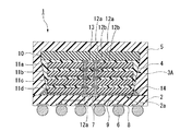
先ず、本発明を適用して製造される半導体装置の一例として、図1に示すCoC型の半導体パッケージ1について説明する。
この半導体パッケージ1は、図1に示すように、配線基板2と、この配線基板2の一面(上面)に実装されたチップ積層体3Aと、このチップ積層体3Aを封止する第1の封止体4と、この第1の封止体4を覆った状態で配線基板2の一面を封止する第2の封止体5と、配線基板2の他面(下面)に配置された複数のはんだボール(外部接続端子)6とを備えることによって、BGA(Ball Grid Array)と呼ばれるパッケージ構造を有している。
(Semiconductor device)
First, a CoC type semiconductor package 1 shown in FIG. 1 will be described as an example of a semiconductor device manufactured by applying the present invention.
As shown in FIG. 1, the semiconductor package 1 includes a
配線基板2は、平面視で矩形状を為すプリント配線板からなり、このプリント配線板は、例えばガラスエポキシ樹脂等からなる絶縁基材の面上にCu等の導電材料からなる導体パターン等を形成し、その表面をソルダーレジスト等の絶縁膜で被覆したものからなる。なお、本例では、厚み0.2mm程度の配線基板2を用いている。
The
この配線基板2の上面中央部には、チップ積層体3Aが実装される実装領域2aが設けられている。また、配線基板2の実装領域2aには、複数のパッド電極(第3の接続端子)7が並んで設けられている。一方、配線基板2の他面(下面)には、複数の接続ランド8が並んで設けられている。そして、上記はんだボール6は、これら接続ランド8の上に配置されている。その他にも、配線基板2には、パッド電極7と接続ランド8との間を電気的に接続するためのビア(貫通電極)や配線パターンなどの引回し配線部9(図1中において模式的に示す。)が設けられている。また、配線基板2の表面は、上述したパッド電極7や接続ランド8が形成された部分を除いて、絶縁膜(図示せず。)で被覆されている。
A
チップ積層体3Aは、キャリア基板10の上に複数(本例では4つ)の半導体チップ11a〜11dが積層されたものからなる。このうち、キャリア基板10は、平面視で矩形状を為すと共に、上記配線基板2よりも小さいプリント配線板からなる。また、このキャリア基板10には、上記配線基板2と同じ材質で同じ厚みのプリント配線板を用いている。また、このキャリア基板10は、一面側に複数の第1のバンプ電極(第1の接続端子)12aを有している。
The chip stacked body 3 </ b> A is formed by stacking a plurality (four in this example) of
一方、複数の半導体チップ11a〜11dは、平面視で矩形状を為すと共に、キャリア基板10よりも小さい形状を有している。また、各半導体チップ11a〜11dは、それぞれ一面側に複数の第1のバンプ電極(第1の接続端子)12aと、他面側に複数の第2のバンプ電極(第2の接続端子)12bと、これら第1のバンプ電極12aと第2のバンプ電極12bとの間を接続する複数の貫通電極(TSV)13とを有している。なお、本例では、厚み50μm程度の半導体チップ11a〜11dを用いている。
On the other hand, the plurality of
そして、これらキャリア基板10及び複数の半導体チップ11a〜11dは、それぞれの一面と他面とを対向させながら、それぞれの間にある第1のバンプ電極12aと第2のバンプ電極12bとを接合して積層されることによって、チップ積層体3Aを構成している。
Then, the
また、このチップ積層体3Aは、最上層に位置する半導体チップ11dを下方に向けた状態で、この半導体チップ11dの他面と配線基板2の一面(実装領域2a)とを対向させながら、その間にある第1のバンプ電極12aとパッド電極7とを接合することによって、配線基板2の一面に実装されている。さらに、このチップ積層体3Aは、配線基板2の一面と半導体チップ11dの他面との間に充填された絶縁性の接着部材14を介して配線基板2の実装領域2aに接着固定されている。なお、チップ積層体3Aは、配線基板2のパッド電極7上にワイヤーバンプ(接合部材)を設けて、このワイヤーバンプを介して第2のバンプ電極12bとパッド電極7とを接合することによって、配線基板2の一面に実装することも可能である。
Further, the chip stacked
第1の封止体4は、チップ積層体3Aを構成するキャリア基板10及び複数の半導体チップ11a〜11dの各隙間に充填されたアンダーフィル材によって、チップ積層体3Aを封止している。
The
第2の封止体5は、第1の封止体4で封止されたチップ積層体3Aの全体を覆うモールド樹脂によって、配線基板2の一面側を全面的に封止している。
The
以上のような構造を有する半導体パッケージ1では、配線基板2とキャリア基板10との間で複数の半導体チップ11a〜11dを挟み込むようにチップ積層体3Aを配線基板2の一面に実装することで、実装後の加熱より各半導体チップ11a〜11dを厚み方向に貫通する貫通電極13が熱膨張した場合に、各半導体チップ11a〜11dに加わる応力を配線基板2とキャリア基板10が受けることになる。すなわち、一旦硬化されたアンダーフィル材の熱履歴による応力の集中箇所がキャリア基板10となる。これにより、各半導体チップ11a〜11dに加わる応力を低減し、これら半導体チップ11a〜11dにクラック等が発生することを抑制することが可能である。
In the semiconductor package 1 having the above structure, the
また、この半導体パッケージ1では、各半導体チップ11a〜11dの接合部分に加わるストレスも低減できる。特に、配線基板2とキャリア基板10に同じ材質のものを用い、更に厚みを等しくすることで、これら配線基板2とキャリア基板10との間で熱膨張係数の差異による応力を低減できる。これにより、配線基板2とキャリア基板10との間に挟み込まれた半導体チップ11a〜11dの接合部分が破断したり、半導体チップ11a〜11dに反り等の変形が発生したりすることを抑制し、半導体パッケージ1の接続信頼性を高めることが可能である。
Moreover, in this semiconductor package 1, the stress added to the junction part of each
(半導体装置の製造方法)
次に、本発明を適用した半導体装置の製造方法として、上記図1に示す半導体パッケージ1の製造工程について説明する。
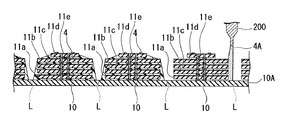
上記半導体パッケージ1を製造する際は、先ず、図2A〜図2Dに示すように、キャリア基板10の上に複数の半導体チップ11a〜11eを積層したチップ積層体3Aを形成する。
(Method for manufacturing semiconductor device)
Next, a manufacturing process of the semiconductor package 1 shown in FIG. 1 will be described as a manufacturing method of the semiconductor device to which the present invention is applied.
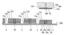
When manufacturing the semiconductor package 1, first, as shown in FIGS. 2A to 2D, a chip stacked body 3 </ b> A in which a plurality of
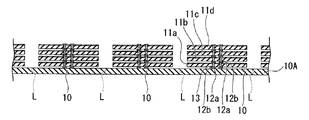
具体的には、先ず、図2Aに示すように、上記キャリア基板10となる部分が複数並んで設けられた母キャリア基板10Aを用意する。この母キャリア基板10Aは、例えばガラスエポキシ基板からなり、上記キャリア基板10となる部分がマトリックス状に複数並んで形成されると共に、最終的にダイシングラインLに沿って切断することで、上記キャリア基板10となる部分を個々のキャリア基板10として切り出すことが可能となっている。
Specifically, first, as shown in FIG. 2A, a
次に、図2Bに示すように、図示を省略する吸着ステージ上に、上記複数の第1のバンプ電極12aが形成された面(一面)を上方に向けた状態で、母キャリア基板10Aを載置する。そして、この母キャリア基板10Aは、吸着ステージに設けられた複数の吸引孔により吸引されながら、この吸着ステージ上に保持される。
Next, as shown in FIG. 2B, the
この状態から、母キャリア基板10A上の上記キャリア基板10となる部分に、ボンディングツール100を用いて、1層目の半導体チップ11aを積層搭載(フリップチップ実装)する。
From this state, the
このフリップチップ実装では、ボンディングツール100に設けられた吸引孔101により1層目の半導体チップ11aを吸引保持しながら、このボンディングツール100が半導体チップ11aを第2のバンプ電極12bが形成された面(他面)を下方に向けた状態で保持する。
In this flip chip mounting, the first
このボンディングツール100は、1層目の半導体チップ11aの他面と、その下にある上記キャリア基板10となる部分の一面とを対向させながら、その間にある第1のバンプ電極12aと第2のバンプ電極12bとの位置を合わせた状態で、1層目の半導体チップ11aを上記キャリア基板10となる部分に載置する。そして、この状態でボンディングツール100が加熱しながら荷重を加えることによって、第1のバンプ電極12aと第2のバンプ電極12bとを熱圧着により接合(フリップチップボンディング)する。なお、この接合時には、荷重だけでなく、超音波も印加するようにしてもよい。
The
これにより、第1のバンプ電極12aと第2のバンプ電極12bとの間が電気的に接続(フリップチップ接続)されて、1層目の半導体チップ11aが上記キャリア基板10となる部分にフリップチップ実装される。
As a result, the
この状態から更に、上述した1層目の半導体チップ11aをフリップチップ実装する場合と同様の方法を用いて、この1層目の半導体チップ11a上に2層目の半導体チップ11bと、この2層目の半導体チップ11b上に3層目の半導体チップ11cと、この3層目の半導体チップ11c上に4層目の半導体チップ11dとを、順にフリップチップ実装する。そして、このようなボンディングツール100を用いた操作を、母キャリア基板10Aの上記キャリア基板10となる部分毎に繰り返す。
From this state, the second
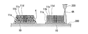
次に、図2Cに示すように、母キャリア基板10A上に積層された複数の半導体チップ11a〜11dの各隙間に、液状のアンダーフィル材4Aを供給するディスペンサー200を用いて、上記第1の封止体4となるアンダーフィル材4Aを充填する。
Next, as shown in FIG. 2C, the
このとき、アンダーフィル材4Aは、毛細管現象により各隙間に浸透しながら充填される。また、各隙間から周囲にはみ出したアンダーフィル材4Aは、上層側から下層側に向かって漸次幅方向に広がった形状となる。
At this time, the
この状態から、アンダーフィル材4Aを例えば150℃程度で加熱(キュア)することで、このアンダーフィル材4Aを硬化させる。これにより、母キャリア基板10Aの上記キャリア基板10となる部分に積層された複数の半導体チップ11a〜11dの各隙間が上記第1の封止体4により封止される。そして、このようなディスペンサー200を用いた操作を、母キャリア基板10Aの上記キャリア基板10となる部分毎に繰り返す。
From this state, the
次に、図2Dに示すように、母キャリア基板10Aの他面側にダイシングテープ300を貼着した後、ダイシングブレード400を用いて、母キャリア基板10Aをダイシングテープ300とは反対側からダイシングラインLに沿って切断し、上記キャリア基板10となる部分を個々のチップ積層体3Aに分割する。これにより、上記第1の封止体4により封止されたチップ積層体3Aを得ることができる。そして、このチップ積層体3Aは、ダイシングテープ300から引き剥がされた後、図示を省略する収納用トレイに収容されて、次工程へと送られる。
Next, as shown in FIG. 2D, after the dicing
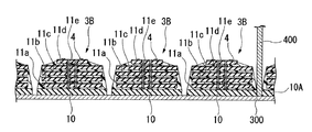
次に、図3に示すように、上記配線基板2となる部分が複数並んで形成された母配線基板2Aを用意する。この母配線基板2Aは、例えばガラスエポキシ基板からなり、上記配線基板2となる部分がマトリックス状に複数並んで形成されると共に、最終的にダイシングラインLに沿って切断することで、上記配線基板2となる部分を個々の配線基板2として切り出すことが可能となっている。
Next, as shown in FIG. 3, a
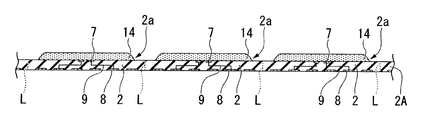
そして、図4に示すように、この母配線基板2Aの一面に、ディスペンサー(図示せず。)を用いて、NCP(Non Conductive Paste)と呼ばれる液状の接着部材14を上記配線基板2となる部分の実装領域2a毎に塗布した後、ボンディングツール500を用いて、上記第1の封止体4により封止されたチップ積層体3Aを母配線基板2Aの上記配線基板2となる部分の実装領域2aにフリップ実装する。
Then, as shown in FIG. 4, a liquid
このフリップチップ実装では、ボンディングツール500の吸引孔501によりチップ積層体3Aを吸引保持しながら、このボンディングツール500がキャリア基板10を上方に向けた状態でチップ積層体3Aを保持する。
In this flip chip mounting, the
このボンディングツール500は、半導体チップ11dの他面と上記配線基板2となる部分の実装領域2aとを対向させながら、その間にある第1のバンプ電極12aとパッド電極7との位置を合わせた状態で、上記第1の封止体4により封止されたチップ積層体3Aを上記配線基板2となる部分の実装領域2a上に載置する。そして、この状態でボンディングツール500が加熱しながら荷重を加えることによって、第1のバンプ電極12aとパッド電極7とを熱圧着により接合(フリップチップボンディング)する。なお、この接合時には、荷重だけでなく、超音波も印加するようにしてもよい。
The
これにより、第1のバンプ電極12aとパッド電極7との間が電気的に接続(フリップチップ接続)されて、上記第1の封止体4により封止されたチップ積層体3Aが母配線基板2Aの配線基板2となる部分の実装領域2aにフリップチップ実装される。
As a result, the
また、上記接着部材14は、母配線基板2Aの一面と半導体チップ11dの他面との間からはみ出した状態で硬化される。これにより、上記第1の封止体4により封止されたチップ積層体3Aは、この接着部材14を介して母配線基板2Aの配線基板2となる部分の実装領域2aに接着固定される。そして、このようなボンディングツール500を用いた操作を、母配線基板2Aの上記配線基板2となる部分毎に繰り返す。
The
なお、上記チップ積層体3Aの周囲からはみ出した第1の封止体4は、上記チップ積層体3Aが上記配線基板2となる部分に実装された状態において、下層側から上層側に向かって漸次幅方向に広がる逆テーパー形状となっている。本発明では、このような逆テーパー形状を有する第1の封止体4によって、母配線基板2Aの一面と半導体チップ11dの他面との間からはみ出した接着部材14の這い上がりを抑制できるため、ボンディングツール500への接着部材14の付着に起因するチップ積層体3Aの割れや接合不良等の発生を低減できる。
The
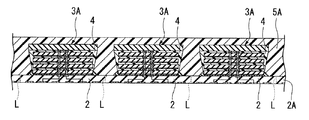
次に、図5に示すように、上記第1の封止体4により封止されたチップ積層体3Aを覆うように母配線基板2Aの一面側を上記第2の封止体5となるモールド樹脂5Aで封止する。具体的には、図示を省略するトランスファモールド装置を用いる。このトランスファモールド装置は、母配線基板2Aの他面側を保持する下金型(固定型)と、母配線基板2Aの一面側に対向してモールド樹脂5Aが充填されるキャビティ空間を形成すると共に、下金型に対して相対的に接離自在に移動される上金型(可動型)とからなる一対の成型金型を備える。
Next, as shown in FIG. 5, a mold in which one surface side of the
そして、このトランスファモールド装置の成形金型に、上記第1の封止体4により封止されたチップ積層体3Aが実装された母配線基板2Aをセットした後、成形金型内のキャビティ空間内に加熱溶融されたモールド樹脂5Aを注入する。このモールド樹脂5Aには、例えばエポキシ樹脂等の熱硬化性樹脂が用いられる。
Then, after setting the
そして、この状態で、モールド樹脂5Aを所定の温度(例えば180℃程度)で加熱(キュア)することで、モールド樹脂5Aを硬化させる。さらに、所定の温度でベークすることで、モールド樹脂5Aが完全に硬化される。これにより、母配線基板2Aの一面側が上記第2の封止体5となるモールド樹脂5Aで完全に封止される。
In this state, the
本発明では、上述したように、第1の封止体4で封止されたチップ積層体3Aを母配線基板2A上に実装した後、この母配線基板2A上を上記第2の封止体5となるモールド樹脂5Aで一括的に封止することで、ボイド(気泡)の発生を低減できる。
In the present invention, as described above, after the chip laminated
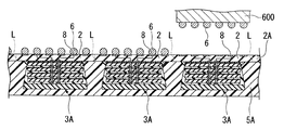
次に、図6に示すように、母配線基板2Aの各配線基板2となる部分に設けられた上記接続ランド8上に、上記はんだボール6を配置する。具体的には、複数の吸着孔(図示せず。)が形成されたボールマウンターのマウントツール600を用いて、複数のはんだボール6をマウントツール600で吸着保持しながら、これら複数のはんだボール6にフラックスを転写形成した後、母配線基板2Aの各配線基板2となる部分毎にはんだボール6を接続ランド8上に載置する。そして、母配線基板2Aの全ての配線基板2となる部分にはんだボール6を載置した後、この母配線基板2Aをリフローする。これにより、母配線基板2Aの各配線基板2となる部分の接続ランド8上に、はんだボール6が配置される。
Next, as shown in FIG. 6, the
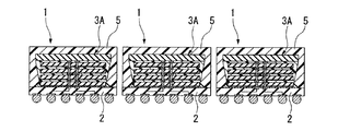
次に、図7に示すように、母配線基板2Aを配線基板2となる部分毎に切断することによって個々の半導体パッケージ1に分割する。具体的には、母配線基板2Aの第2の封止体5側にダイシングテープ700を貼着した後、ダイシングブレード800を用いて母配線基板2Aをダイシングテープ700とは反対側からダイシングラインLに沿って切断する。これにより、半導体パッケージ1毎に分割される。そして、図8に示すように、これら半導体パッケージ1をダイシングテープ700から引き剥がすことで、複数の半導体パッケージ1を一括して製造することができる。
Next, as shown in FIG. 7, the
以上のように、本発明では、母配線基板2Aとキャリア基板10との間で複数の半導体チップ11a〜11dを挟み込むようにチップ積層体3Aを配線基板2となる部分に実装することで、実装後の封止工程やリフロー工程等の加熱より各半導体チップ11a〜11dを厚み方向に貫通する貫通電極13が熱膨張した場合でも、各半導体チップ11a〜11dに加わる応力を低減し、これら半導体チップ11a〜11dにクラック等が発生することを抑制することが可能である。
As described above, in the present invention, the
また、本発明では、各半導体チップ11a〜11dの接合部分に加わるストレスも低減できる。特に、母配線基板2Aとキャリア基板10に同じ材質のものを用い、更に厚みを等しくすることで、これら母配線基板2Aとキャリア基板10との間で熱膨張係数の差異による応力を低減できる。これにより、母配線基板2Aとキャリア基板10との間に挟み込まれた半導体チップ11a〜11dの接合部分が破断したり、半導体チップ11a〜11dに反り等の変形が発生したりすることを抑制し、上記半導体パッケージ1の接続信頼性を高めることが可能である。
Moreover, in this invention, the stress added to the junction part of each
また、本発明では、上述した吸着ステージ上に母キャリア基板10Aを保持しながら、この母キャリア基板10A上にボンディングツール100を用いて半導体チップ11a〜11dをフリップ実装することで、従来のような高温(例えば300℃程度)による熱圧着が不要となり、例えば常温〜150℃程度での超音波接合が可能となるため、半導体チップ11a〜11dへの熱の影響を低減できる。
Further, in the present invention, while holding the
また、本発明では、母キャリア基板10Aを切断して個々のチップ積層体3Aに分割するまで、この母キャリア基板10Aのまま取り扱うことができるため、組立工程の効率化を図ることが可能である。
Further, in the present invention, since the
なお、本発明は、上記実施形態のものに必ずしも限定されるものではなく、本発明の趣旨を逸脱しない範囲において種々の変更を加えることが可能である。
例えば、上記実施形態では、上記チップ積層体3Aを第1の封止体4で封止する工程を、母キャリア基板10Aを切断して個々のチップ積層体3Aに分割する工程の前に行う場合について説明したが、本発明では、上記チップ積層体3Aを第1の封止体4で封止する工程を、母キャリア基板10Aを切断して個々のチップ積層体3Aに分割する工程の後に行うことも可能である。
In addition, this invention is not necessarily limited to the thing of the said embodiment, A various change can be added in the range which does not deviate from the meaning of this invention.
For example, in the above embodiment, the step of sealing the
具体的には、図9Aに示すように、上述した母キャリア基板10Aの上記キャリア基板10となる部分毎に複数の半導体チップ11a〜11dを積層した状態から、図9Bに示すように、母キャリア基板10Aの他面側にダイシングテープ300を貼着した後、ダイシングブレード400を用いて、母キャリア基板10AをダイシングラインLに沿って切断し、上記キャリア基板10に分割する。
Specifically, as shown in FIG. 9A, from the state in which a plurality of
そして、図9Cに示すように、キャリア基板10上に積層された複数の半導体チップ11a〜11dの各隙間に、液状のアンダーフィル材4Aを供給するディスペンサー200を用いて、上記第1の封止体4となるアンダーフィル材4Aを充填した後、このアンダーフィル材4Aを硬化させる。これにより、上記第1の封止体4により封止されたチップ積層体3Aを得ることができる。
Then, as shown in FIG. 9C, the first sealing is performed using a
そして、この第1の封止体4により封止されたチップ積層体3Aは、図9Dに示すように、ダイシングテープ300から引き剥がされた後、上記図4に示す工程と同様に、ボンディングツール500を用いて、半導体チップ11dの第1のバンプ電極12aとパッド電極7との間を電気的に接続(フリップチップ接続)しながら、母配線基板2Aの上記配線基板2となる部分の実装領域2aにフリップ実装されることになる。
Then, after the
本発明では、上述したように、母配線基板2Aとキャリア基板10との間で複数の半導体チップ11a〜11dを挟み込むようにチップ積層体3Aを母配線基板2Aの一面に実装することで、実装後の加熱により各半導体チップ11a〜11dに加わる応力を低減し、これら半導体チップ11a〜11dにクラック等が発生することを抑制することが可能である。また、各半導体チップ11a〜11dの接合部分に加わるストレスも低減できるため、この接合部分が破断したり、半導体チップ11a〜11dに反り等の変形が発生したりすることを抑制し、半導体パッケージ1の接続信頼性を高めることが可能である。
In the present invention, as described above, the
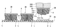
また、本発明では、上記チップ積層体3Aの構成に必ずしも限定されるものではなく、例えば図10A〜図10Dに示すようなチップ積層体3Bを配線基板2上に実装することも可能である。
Moreover, in this invention, it is not necessarily limited to the structure of the said chip laminated
具体的に、このチップ積層体3Bは、上記キャリア基板10の上に、DRAM(Dynamic Random Access Memory)回路などが形成された複数(本例では4つ)のメモリーチップ(第1の半導体チップ)11a〜11dと、この上に、各メモリーチップ11a〜11dと配線基板2との間のインターフェースを取るためのIF(InterFace)回路などが形成されたIFチップ(第2の半導体チップ)11eとを積層した構造を有している。
Specifically, the
このうち、複数のメモリーチップ11a〜11dは、平面視で矩形状を為すと共に、配線基板2よりも小さい形状を有している。また、各メモリーチップ11a〜11dは、それぞれ一面側に複数の第1のバンプ電極(第1の接続端子)12aと、他面側に複数の第2のバンプ電極(第2の接続端子)12bと、これら第1のバンプ電極12aと第2のバンプ電極12bとの間を接続する複数の貫通電極(TSV)13とを有している。
Among these, the plurality of
そして、図10Aに示すように、これら複数のメモリーチップ11a〜11dは、上記図2Bに示す場合と同様に、母キャリア基板10A上の上記キャリア基板10となる部分に、ボンディングツール100を用いて、それぞれの一面と他面とを対向させながら、それぞれの間にある第1のバンプ電極12aと第2のバンプ電極12bとを接合して積層される。
Then, as shown in FIG. 10A, the plurality of
一方、IFチップ11eは、平面視で矩形状を為すと共に、上記メモリーチップ11a〜11dよりも小さい形状を有している。また、IFチップ11eは、その一面側に複数の第1のバンプ電極(第1の接続端子)12aと、その他面側に複数の第2のバンプ電極(第2の接続端子)12bと、これら第1のバンプ電極12aと第2のバンプ電極12bとの間を接続する複数の貫通電極(TSV)13とを有している。
On the other hand, the
そして、図10Aに示すように、このIFチップ11eは、ボンディングツール100を用いて、その他面と、上記メモリーチップ11dの一面とを対向させながら、その間にある第1のバンプ電極12aと第2のバンプ電極12bとを接合して積層される。
Then, as shown in FIG. 10A, the
なお、IFチップ11eの第1のバンプ電極12aは、配線基板2のパッド電極7との間隔に合わせて、上記メモリーチップ11a〜11dの第1のバンプ電極12aよりも広い間隔(200μm以上)を有している。このため、IFチップ11eでは、第1のバンプ電極12aと貫通電極13との間に、再配線のための配線パターン15を設けて、配線基板2のパッド電極7との間隔調整を行っている。
The
そして、母キャリア基板10A上に複数のメモリーチップ11a〜11d及びIFチップ11eを積層した後は、図10Bに示すように、これら複数のメモリーチップ11a〜11d及びIFチップ11eの各隙間に、液状のアンダーフィル材4Aを供給するディスペンサー200を用いて、上記第1の封止体4となるアンダーフィル材4Aを充填した後、このアンダーフィル材4Aを硬化させる。
Then, after the plurality of
その後は、図10Cに示すように、上記図2Dに示す工程と同様に、母キャリア10Aの他面側にダイシングテープ300を貼着した後、ダイシングブレード400を用いて、母キャリア基板10Aをダイシングテープ300とは反対側からダイシングラインLに沿って切断し、上記キャリア基板10となる部分を個々のチップ積層体3Bに分割する。これにより、上記第1の封止体4により封止されたチップ積層体3Bを得ることができる。
Thereafter, as shown in FIG. 10C, after the dicing
そして、このチップ積層体3Bは、図10Dに示すように、ダイシングテープ300から引き剥がされた後、上記図4に示す工程と同様に、ボンディングツール500を用いて、IFチップ11eの第1のバンプ電極12aとパッド電極7との間を電気的に接続(フリップチップ接続)しながら、母配線基板2Aの上記配線基板2となる部分の実装領域2aにフリップ実装されることになる。
Then, as shown in FIG. 10D, the
本発明では、母配線基板2Aとキャリア基板10との間で複数のメモリーチップ11a〜11d及びIFチップ11eを挟み込むようにチップ積層体3Bを母配線基板2Aの一面に実装することで、実装後の加熱により各半導体チップ11a〜11eに加わる応力を低減し、これら半導体チップ11a〜11eにクラック等が発生することを抑制することが可能である。また、各半導体チップ11a〜11eの接合部分に加わるストレスも低減できるため、この接合部分が破断したり、半導体チップ11a〜11eに反り等の変形が発生したりすることを抑制し、半導体パッケージ1の接続信頼性を高めることが可能である。
In the present invention, the
なお、上記チップ積層体3Bは、メモリーチップ11a〜11dとIFチップ11eとを組み合わせた構成となっているが、チップの種類や大きさ等については任意に変更することが可能である。
In addition, although the said chip laminated
また、本発明では、上述した4段構成や5段構成のチップ積層体3A,3Bの構成に必ずしも限定されるものではなく、チップ積層体の積層数については少なくとも2段以上であればよく、4段以下や6段以上としてもよい。また、第1のバンプ電極12a、貫通電極13及び第2のバンプ電極12bの配置や数についても、上記チップ積層体3A,3Bの構成に限らず、適宜変更して実施することが可能である。
Further, in the present invention, it is not necessarily limited to the configuration of the
また、本発明は、上記BGA型の半導体パッケージ1に限らず、例えば、LGA(Land Grid Array)型やCSP(Chip Size Package)型などの他の半導体パッケージにも適用可能である。 The present invention is not limited to the BGA type semiconductor package 1 described above, and can be applied to other semiconductor packages such as an LGA (Land Grid Array) type and a CSP (Chip Size Package) type.
1…半導体パッケージ(半導体装置) 2…配線基板 2A…母配線基板 2a…実装領域 2A…母配線基板 3A,3B…チップ積層体 4…第1の封止体 4A…アンダーフィル材 5…第2の封止体 5A…モールド樹脂 6…はんだボール(外部接続端子) 7…パッド電極(第3の接続端子) 8…接続ランド 9…引回し配線部 10…キャリア基板 10A…母キャリア基板 11a〜11d…メモリーチップ(半導体チップ) 11e…IFチップ(半導体チップ) 12a…第1のバンプ電極(第1の接続端子) 12b…第2のバンプ電極(第2の接続端子) 13…貫通電極 14…接着部材 100…ボンディングツール 200…ディスペンサー 300…ダイシングテープ 400…ダイシングブレード 500…ボンディングツール 600…マウントツール 700…ダイシングテープ 800…ダイシングブレード
DESCRIPTION OF SYMBOLS 1 ... Semiconductor package (semiconductor device) 2 ...
Claims (9)
前記キャリア基板及び前記複数の半導体チップの各隙間に第1の封止体を充填しながら、前記チップ積層体を第1の封止体で封止する工程と、
前記配線基板となる部分が複数並んで形成された母配線基板の一面に、この母配線基板と前記キャリア基板との間で前記複数の半導体チップを挟み込むように、前記チップ積層体を前記配線基板となる部分毎に実装する工程と、
前記第1の封止体で封止されたチップ積層体の全体を覆うように前記母配線基板の一面側を第2の封止体で封止する工程と、
前記母配線基板を前記配線基板となる部分毎に切断することによって個々の半導体装置に分割する工程とを含むことを特徴とする半導体装置の製造方法。 Forming a chip stack in which a plurality of semiconductor chips are stacked on a carrier substrate;
Sealing the chip stack with the first sealing body while filling the gaps between the carrier substrate and the plurality of semiconductor chips with the first sealing body;
The chip stack is placed on one surface of the mother wiring board in which a plurality of portions to be the wiring board are arranged side by side so as to sandwich the plurality of semiconductor chips between the mother wiring board and the carrier substrate. A process of mounting each part to become,
Sealing one surface side of the mother wiring substrate with a second sealing body so as to cover the entire chip stack sealed with the first sealing body;
A step of dividing the mother wiring board into individual semiconductor devices by cutting each portion to be the wiring board.
前記母キャリア基板を前記キャリア基板となる部分毎に切断することによって個々のチップ積層体に分割する工程とを含むことを特徴とする請求項1に記載の半導体装置の製造方法。 In the step of forming the chip stack, the plurality of semiconductor chips are sequentially stacked on each surface of the mother carrier substrate provided with a plurality of portions to be the carrier substrate, and each of the portions to be the carrier substrate is mounted. Process,
2. The method of manufacturing a semiconductor device according to claim 1, further comprising: dividing the mother carrier substrate into individual chip stacks by cutting each portion to be the carrier substrate. 3.
Priority Applications (1)
| Application Number | Priority Date | Filing Date | Title |
|---|---|---|---|
| JP2011004758A JP2012146853A (en) | 2011-01-13 | 2011-01-13 | Method of manufacturing semiconductor device |
Applications Claiming Priority (1)
| Application Number | Priority Date | Filing Date | Title |
|---|---|---|---|
| JP2011004758A JP2012146853A (en) | 2011-01-13 | 2011-01-13 | Method of manufacturing semiconductor device |
Publications (1)
| Publication Number | Publication Date |
|---|---|
| JP2012146853A true JP2012146853A (en) | 2012-08-02 |
Family
ID=46790123
Family Applications (1)
| Application Number | Title | Priority Date | Filing Date |
|---|---|---|---|
| JP2011004758A Withdrawn JP2012146853A (en) | 2011-01-13 | 2011-01-13 | Method of manufacturing semiconductor device |
Country Status (1)
| Country | Link |
|---|---|
| JP (1) | JP2012146853A (en) |
Cited By (7)
| Publication number | Priority date | Publication date | Assignee | Title |
|---|---|---|---|---|
| JP2014183278A (en) * | 2013-03-21 | 2014-09-29 | Toshiba Corp | Semiconductor device and manufacturing method of the same |
| CN104916551A (en) * | 2014-03-14 | 2015-09-16 | 株式会社东芝 | Semiconductor device manufacturing method and semiconductor device |
| KR20160100923A (en) * | 2013-12-23 | 2016-08-24 | 인텔 코포레이션 | Through-body-via isolated coaxial capacitor and techniques for forming same |
| US9595507B2 (en) | 2015-03-11 | 2017-03-14 | Kabushiki Kaisha Toshiba | Semiconductor device and method of manufacturing the same |
| US9601465B2 (en) | 2013-10-16 | 2017-03-21 | Samsung Electronics Co., Ltd. | Chip-stacked semiconductor package and method of manufacturing the same |
| KR20170098586A (en) * | 2016-02-22 | 2017-08-30 | 삼성전자주식회사 | Semiconductor package |
| US9905550B2 (en) | 2014-07-11 | 2018-02-27 | Samsung Electronics Co., Ltd. | Semiconductor package and method of fabricating the same |
-
2011
- 2011-01-13 JP JP2011004758A patent/JP2012146853A/en not_active Withdrawn
Cited By (11)
| Publication number | Priority date | Publication date | Assignee | Title |
|---|---|---|---|---|
| JP2014183278A (en) * | 2013-03-21 | 2014-09-29 | Toshiba Corp | Semiconductor device and manufacturing method of the same |
| US9601465B2 (en) | 2013-10-16 | 2017-03-21 | Samsung Electronics Co., Ltd. | Chip-stacked semiconductor package and method of manufacturing the same |
| US9905538B2 (en) | 2013-10-16 | 2018-02-27 | Samsung Electronics Co., Ltd. | Chip-stacked semiconductor package and method of manufacturing the same |
| KR20160100923A (en) * | 2013-12-23 | 2016-08-24 | 인텔 코포레이션 | Through-body-via isolated coaxial capacitor and techniques for forming same |
| KR102230011B1 (en) * | 2013-12-23 | 2021-03-19 | 인텔 코포레이션 | Through-body-via isolated coaxial capacitor and techniques for forming same |
| CN104916551A (en) * | 2014-03-14 | 2015-09-16 | 株式会社东芝 | Semiconductor device manufacturing method and semiconductor device |
| US9905550B2 (en) | 2014-07-11 | 2018-02-27 | Samsung Electronics Co., Ltd. | Semiconductor package and method of fabricating the same |
| US9595507B2 (en) | 2015-03-11 | 2017-03-14 | Kabushiki Kaisha Toshiba | Semiconductor device and method of manufacturing the same |
| KR20170098586A (en) * | 2016-02-22 | 2017-08-30 | 삼성전자주식회사 | Semiconductor package |
| KR102579876B1 (en) | 2016-02-22 | 2023-09-18 | 삼성전자주식회사 | Semiconductor package |
| US11894346B2 (en) | 2016-02-22 | 2024-02-06 | Samsung Electronics Co., Ltd. | Semiconductor package having a high reliability |
Similar Documents
| Publication | Publication Date | Title |
|---|---|---|
| JP5570799B2 (en) | Semiconductor device and manufacturing method thereof | |
| JP5579402B2 (en) | Semiconductor device, method for manufacturing the same, and electronic device | |
| US8575763B2 (en) | Semiconductor device and method of manufacturing the same | |
| JP5543125B2 (en) | Semiconductor device and manufacturing method of semiconductor device | |
| US20140295620A1 (en) | Method of manufacturing semiconductor device having plural semiconductor chips stacked one another | |
| WO2014181766A1 (en) | Semiconductor device and semiconductor device manufacturing method | |
| JP2010251347A (en) | Method of manufacturing semiconductor device | |
| JP2012212786A (en) | Manufacturing method of semiconductor device | |
| JP2010245383A (en) | Semiconductor device and method of manufacturing the same | |
| JP2012069903A (en) | Semiconductor device, and method of manufacturing the same | |
| JP2012142536A (en) | Semiconductor device and manufacturing method of the same | |
| JP2012146853A (en) | Method of manufacturing semiconductor device | |
| JP2012109437A (en) | Semiconductor device and method of manufacturing the same | |
| JP2015005637A (en) | Semiconductor device | |
| JP2014007228A (en) | Semiconductor device and manufacturing method of the same | |
| JP2011187574A (en) | Semiconductor device and method of manufacturing the same, and electronic device | |
| JP2012209449A (en) | Method of manufacturing semiconductor device | |
| US10553560B2 (en) | Semiconductor device having multiple semiconductor chips laminated together and electrically connected | |
| JP2013021058A (en) | Manufacturing method of semiconductor device | |
| JP2015008210A (en) | Method of manufacturing semiconductor device | |
| JP2011243724A (en) | Semiconductor device and method for manufacturing the same | |
| KR101494411B1 (en) | Semiconductor package, and method of manufacturing the same | |
| JP2012059730A (en) | Semiconductor device, and method of manufacturing the same | |
| TW201448071A (en) | Chip stack, semiconductor devices having the same, and manufacturing methods for chip stack | |
| JP2012015446A (en) | Method of manufacturing semiconductor device |
Legal Events
| Date | Code | Title | Description |
|---|---|---|---|
| A711 | Notification of change in applicant |
Free format text: JAPANESE INTERMEDIATE CODE: A711 Effective date: 20130731 |
|
| A521 | Request for written amendment filed |
Free format text: JAPANESE INTERMEDIATE CODE: A821 Effective date: 20130801 |
|
| A521 | Request for written amendment filed |
Free format text: JAPANESE INTERMEDIATE CODE: A523 Effective date: 20130905 |
|
| RD02 | Notification of acceptance of power of attorney |
Free format text: JAPANESE INTERMEDIATE CODE: A7422 Effective date: 20131108 |
|
| RD04 | Notification of resignation of power of attorney |
Free format text: JAPANESE INTERMEDIATE CODE: A7424 Effective date: 20131219 |
|
| A300 | Application deemed to be withdrawn because no request for examination was validly filed |
Free format text: JAPANESE INTERMEDIATE CODE: A300 Effective date: 20140401 |