JP2012142483A - Ceramic substrate manufacturing method and ceramic sintered laminate - Google Patents
Ceramic substrate manufacturing method and ceramic sintered laminate Download PDFInfo
- Publication number
- JP2012142483A JP2012142483A JP2011000484A JP2011000484A JP2012142483A JP 2012142483 A JP2012142483 A JP 2012142483A JP 2011000484 A JP2011000484 A JP 2011000484A JP 2011000484 A JP2011000484 A JP 2011000484A JP 2012142483 A JP2012142483 A JP 2012142483A
- Authority
- JP
- Japan
- Prior art keywords
- substrate
- ceramic
- sintered
- groove
- unsintered
- Prior art date
- Legal status (The legal status is an assumption and is not a legal conclusion. Google has not performed a legal analysis and makes no representation as to the accuracy of the status listed.)
- Pending
Links
Images


Abstract
Description
本発明は、セラミック基板の製造方法およびセラミック焼結積層体に関する。 The present invention relates to a method for producing a ceramic substrate and a ceramic sintered laminate.
近年、セラミック基板の製造歩留まりを向上させる技術が求められている(例えば、特許文献1参照)。 In recent years, a technique for improving the manufacturing yield of ceramic substrates has been demanded (see, for example, Patent Document 1).
本発明は、上記に鑑みてなされたものであって、製造歩留まりの向上に寄与することが可能な、セラミック基板の製造方法およびセラミック焼結積層体を提供することを目的とする。 This invention is made | formed in view of the above, Comprising: It aims at providing the manufacturing method and ceramic sintered laminated body of a ceramic substrate which can contribute to the improvement of a manufacturing yield.
本発明の一実施形態に係るセラミック基板の製造方法は、平面視したときにマトリックス状に形成された第1溝を有する第1セラミック材料からなる第1未焼結基板と、平面視したときにマトリックス状に形成された第2溝を有する、前記第1セラミック材料と異なる第2セラミック材料からなる第2未焼結基板とを含み、平面視して前記第1溝と前記第2溝とを重ねるようにして積層した未焼結積層体を準備する工程と、前記未焼結積層体を焼成して、前記第1溝および前記第2溝が収縮した第1収縮溝および第2収縮溝を有するセラミック焼結積層体を形成する工程と、前記収縮溝に沿って前記セラミック焼結積層体を複数の個片に分割する工程と、を備えている。 A method for manufacturing a ceramic substrate according to an embodiment of the present invention includes a first unsintered substrate made of a first ceramic material having first grooves formed in a matrix when viewed in plan, and a plan view. A second unsintered substrate made of a second ceramic material different from the first ceramic material, and having the second grooves formed in a matrix, and the first grooves and the second grooves in plan view. A step of preparing a non-sintered laminated body laminated so as to overlap; and firing the non-sintered laminated body to form a first shrinking groove and a second shrinking groove in which the first groove and the second groove shrink A step of forming the ceramic sintered laminate, and a step of dividing the ceramic sintered laminate into a plurality of pieces along the shrinkage grooves.
本発明の一実施形態に係るセラミック焼結積層体は、平面視したときにマトリックス状に形成された第1収縮溝を有する第1セラミック材料からなる第1焼結基板と、平面視したときにマトリックス状に形成された第2収縮溝を有する、前記第1セラミック材料と異なる第2セラミック材料からなる第2焼結基板とを含み、平面視して前記第1焼結基板の第1収縮溝と前記第2焼結基板の第2収縮溝とが重なるようにして積層されている、ことを特徴とする。 A ceramic sintered laminate according to an embodiment of the present invention has a first sintered substrate made of a first ceramic material having first shrink grooves formed in a matrix when viewed in plan, and when viewed in plan. A second sintered substrate made of a second ceramic material different from the first ceramic material, and having a second contracted groove formed in a matrix, and the first contracted groove of the first sintered substrate in plan view And the second shrinkage groove of the second sintered substrate are stacked so as to overlap each other.
本発明によれば、製造歩留まりの向上に寄与することが可能な、セラミック基板の製造方法およびセラミック焼結積層体を提供することができる。 ADVANTAGE OF THE INVENTION According to this invention, the manufacturing method of a ceramic substrate and the ceramic sintered laminated body which can contribute to the improvement of a manufacturing yield can be provided.
添付図面を参照して、本発明にかかるセラミック基板の製造方法、セラミック焼結積層体およびセラミック基板の実施形態を説明する。 Embodiments of a ceramic substrate manufacturing method, a ceramic sintered laminate, and a ceramic substrate according to the present invention will be described with reference to the accompanying drawings.
<セラミック基板の製造方法>
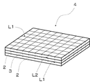
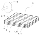
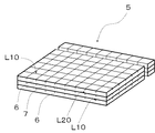
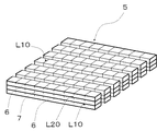
図1から図10は、本実施形態に係るセラミック基板の製造方法の一例を示す概観斜視図である。図1は、未焼結基板の概観斜視図である。図2は、未焼結基板を3層積層する前の状態を示す概観斜視図である。図3は、未焼結積層体の概観斜視図である。図4は、セラミック焼結積層体を切断前の状態を示した概観斜視図である。図5は、セラミック焼結積層体を切断している状態を示した概観斜視図である。図6は、セラミック焼結積層体を1辺に沿って切断した状態を示した概観斜視図である。図7は、セラミック焼結積層体を1辺に沿って複数個に分割した状態を示した概観斜視図である。図8は、セラミック焼結積層体を他辺に沿って切断し、一部を個片にした状態を示した概観斜視図である。図9は、セラミック焼結積層体を個片に分割した状態を示した概観斜視図である。図10は、セラミック焼結積層体を個片にした1つのセラミック基板の概観斜視図である。
<Manufacturing method of ceramic substrate>
1 to 10 are schematic perspective views showing an example of a method for manufacturing a ceramic substrate according to the present embodiment. FIG. 1 is a schematic perspective view of a green substrate. FIG. 2 is a schematic perspective view showing a state before three layers of unsintered substrates are laminated. FIG. 3 is a schematic perspective view of the green laminate. FIG. 4 is an overview perspective view showing a state before cutting the ceramic sintered laminate. FIG. 5 is a schematic perspective view showing a state in which the sintered ceramic laminate is cut. FIG. 6 is a schematic perspective view showing a state in which the sintered ceramic laminate is cut along one side. FIG. 7 is an overview perspective view showing a state in which the ceramic sintered laminate is divided into a plurality of parts along one side. FIG. 8 is a schematic perspective view showing a state in which the ceramic sintered laminate is cut along the other side and partly cut into pieces. FIG. 9 is an overview perspective view showing a state in which the ceramic sintered laminate is divided into individual pieces. FIG. 10 is a schematic perspective view of one ceramic substrate obtained by dividing a ceramic sintered laminate.
本実施形態に係るセラミック基板の製造方法は、一度に複数のセラミック基板を製造する方法である。セラミック基板は、電子部品として用いることができる。 The method for manufacturing a ceramic substrate according to the present embodiment is a method for manufacturing a plurality of ceramic substrates at a time. The ceramic substrate can be used as an electronic component.
セラミック基板1の製造方法としては、平面視したときにマトリックス状に形成された第1溝L1を有する第1セラミック材料からなる第1未焼結基板2と、平面視したときにマトリックス状に形成された第2溝L2を有する、第1セラミック材料と異なる第2セラミック材料からなる第2未焼結基板3とを含み、平面視して第1溝L1と第2溝L2とが重なるようにして積層した未焼結積層体4を準備する。
As a method of manufacturing the
第1未焼結基板2は、例えば、絶縁体の材料からなるものであって、第2未焼結基板3は、例えば、磁性体の材料からなるものである。
The first
第1未焼結基板2は、例えば、絶縁層としてのグリーンシートから作製する。例えば酸化ケイ素、酸化アルミニウム、酸化マグネシウム、酸化亜鉛、酸化カルシウムまたは酸化ホウ素に適当な溶剤、可塑剤およびバインダーを加えて混ぜ合わせて、混合物を得る。そして、この混合物を用いて例えばドクターブレード法により、例えば厚さ10μm以上100μm以下のグリーンシートを形成する。
The first
次に、グリーンシートを例えば平面視して1辺の長さが50mm以上300mm以下の
サイズに切り出す。そして、切り出したグリーンシートに対して、例えばスクリーン印刷法を用いて、電極およびビアホール電極を形成する。電極およびビアホール電極は、例えば、ニッケル、銅、銀、金または白金等の金属材料、あるいはそれらの合金、あるいはこれらの材料のうち複数の材料を混合した複合系材料からなる。さらに、電極およびビアホール電極を形成したグリーンシートの1層、もしくは複数層を積み重ねて、積層絶縁体用成形体を形成する。
Next, the green sheet is cut into a size having a side length of 50 mm or more and 300 mm or less, for example, in plan view. Then, an electrode and a via hole electrode are formed on the cut green sheet using, for example, a screen printing method. The electrode and the via-hole electrode are made of, for example, a metal material such as nickel, copper, silver, gold, or platinum, an alloy thereof, or a composite material obtained by mixing a plurality of these materials. Furthermore, one or more layers of green sheets on which electrodes and via-hole electrodes are formed are stacked to form a laminated insulator molded body.
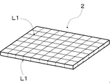
次に、積層絶縁体用成形体に対して、成形体の厚み方向にチップサイズとなるように、マトリックス状に例えばダイシングソーで切り込みを入れて第1溝L1を形成する。このようにして、図1に示すように、第1溝L1を有する第1未焼結基板2を準備することができる。なお、第1溝L1の厚み方向の深さは、例えば、3μm以上70μm以下の切り込みであって、第1未焼結基板2を1枚のシートとして取り扱える深さであればよい。
Next, the first groove L <b> 1 is formed by cutting the laminated insulator molded body into a matrix shape with, for example, a dicing saw so as to have a chip size in the thickness direction of the molded body. Thus, as shown in FIG. 1, the 1st non-sintered board |
また、第2未焼結基板3は、例えば、コイル用の磁性体層として酸化鉄、酸化亜鉛、酸化銅または酸化ニッケルに適当な溶剤、可塑剤およびバインダーを加えて混ぜ合わせて、混合物を得る。そして、この混合物を用いて例えばドクターブレード法により、例えば厚さ10μm以上100μm以下のグリーンシートから作製する。
The second
次に、グリーンシートを例えば平面視して1辺の長さが50mm以上300mm以下のサイズに切り出す。そして、切り出したグリーンシートに対して、例えばスクリーン印刷法を用いて、電極およびビアホール電極を形成する。電極およびビアホール電極は、例えば、ニッケル、銅、銀、金または白金等の金属材料、あるいはそれらの合金、あるいはこれらの材料のうち複数の材料を混合した複合系材料からなる。さらに、電極およびビアホール電極を形成したグリーンシートを複数枚積み重ねて、積層コイル用成形体を形成する。なお、積層コイル用成形体は、平面視したときに積層コイル用成形体のサイズと合わさる大きさに設定する。 Next, the green sheet is cut into a size having a side length of 50 mm or more and 300 mm or less, for example, in plan view. Then, an electrode and a via hole electrode are formed on the cut green sheet using, for example, a screen printing method. The electrode and the via-hole electrode are made of, for example, a metal material such as nickel, copper, silver, gold, or platinum, an alloy thereof, or a composite material obtained by mixing a plurality of these materials. Further, a plurality of green sheets on which electrodes and via-hole electrodes are formed are stacked to form a laminated coil molded body. Note that the laminated coil molded body is set to a size that matches the size of the laminated coil molded body when viewed in plan.
次に、積層コイル用成形体に対して、成形体の厚み方向にチップサイズとなるように、マトリックス状に例えばダイシングソーで切り込みを入れて第2溝L2を形成する。このようにして、第2溝L2を有する第2未焼結基板3を準備することができる。なお、第2未焼結基板3の第2溝L2は、平面視したときに第1未焼結基板2の第1溝L1と合わさるように形成する。なお、第2溝L2は、厚み方向に例えば、3μm以上70μm以下の切り込みであって、第2未焼結基板3を1枚のシートとして取り扱える深さであればよい。
Next, the second groove L <b> 2 is formed by cutting in a matrix shape with a dicing saw, for example, so as to obtain a chip size in the thickness direction of the molded body. In this way, the second
未焼結積層体4は、図2に示すように、少なくとも3層構造であって、未焼結積層体4の最上層および最下層が第1未焼結基板2および第2未焼結基板3のうちどちらか一方であり、未焼結基板4の中間層が第1未焼結基板2および第2未焼結基板3のうちどちらか他方である。また、未焼結積層体4は、3種以上の異なるセラミック材料からなる未焼結基板を積層したり、第1未焼結基板2および第2未焼結基板3を交互に積層したものである。
As shown in FIG. 2, the
ここでは、未焼結積層体の最上層および最下層については、第1未焼結基板2を用いて、未焼結積層体の中間層については、第2未焼結基板3を用いる。
Here, the first
そして、第1未焼結基板2と第2未焼結基板3を例えば熱圧着することで、図3に示すように、積層した未焼結積層体4を得る。未焼結積層体4は、平面視して第1未焼結基板2の第1溝L1と第2未焼結基板3の第2溝L2とが重なるように積層されたものを準備する。
And the 1st non-sintered board |
また、第1未焼結基板2上に、第2未焼結基板3を熱圧着し、さらに第2未焼結基板3上に、別の第1未焼結基板2を熱圧着して未焼結積層体4を得ることができる。
Further, the second
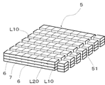
次に、未焼結積層体4を、例えば900℃〜1050℃の温度で焼成する。そして、第1未焼結基板2および第2未焼結基板3を同時に焼成して、セラミック焼結積層体5を得ることができる。なお、第1未焼結基板2が焼結すると、第1焼結基板6となり、第2未焼結基板3が焼結すると、第2焼結基板7となる。このとき、第1未焼結基板2の第1溝L1および第2未焼結基板3の第2溝L2は、熱収縮して収縮溝となる。ここで、第1未焼結基板2の第1溝L1は、熱収縮して第1収縮溝L10となる。また、第2未焼結基板3の第2溝L2は、熱収縮して第2収縮溝L20となる。
Next, the unsintered
ここでは、未焼結積層体4の最上層および最下層に第1未焼結基板2が設けられ、未焼結積層体4の中間層に第2未焼結基板3を設けた構造であって、未焼結積層体4の焼結時に、第1未焼結基板2および第2未焼結基板3の熱収縮率の違いにより、第1未焼結基板2または第2未焼結基板3が異なる熱収縮を起こそうとする。しかしながら、未焼結積層体4の中間層に位置する第2未焼結基板3は、第2未焼結基板3の上面および下面と接する第1未焼結基板2の熱収縮に合わせて第2未焼結基板3が熱収縮を起こす。そして、平面視したときに第1未焼結基板2が焼結した第1焼結基板6の第1収縮溝L10と、第2未焼結基板2が焼結した第2焼結基板7の第2収縮溝L20が重なるように形成される。
Here, the first
このようにして、平面視したときにマトリックス状に形成された第1収縮溝L10を有する第1焼結基板6と、平面視したときにマトリックス状に形成された第2収縮溝L20を有する第2焼結基板7とを含むセラミック焼結積層体5となる。セラミック焼結積層体5は、平面視して第1焼結基板6の第1収縮溝L10と第2焼結基板7の第2収縮溝L20が重なるように形成される。その結果、例えばブレード8を用いて、セラミック焼結積層体5を個片化するときに、第1焼結基板6および第2焼結基板7を効率よく複数のセラミック基板とすることができる。
In this way, the first
次に、収縮溝に沿ってセラミック焼結積層体5を複数の個片に分割する。ここでは、セラミック焼結積層体5を、例えばブレード8を用いて個片化する。なお、ブレード8を用いて、セラミック焼結積層体5を個片化する方法を説明するが、レーザーを用いたり、溝部に折り曲げ力を作用させたりして、セラミック焼結積層体5を個片化してもよい。
Next, the ceramic
ブレード8は、例えば、金属材料またはセラミック材料からなり、セラミック焼結積層体5を個片化できる硬度を有するものを用いる。
The
ここで、図4に示すように、セラミック焼結積層体5の第1収縮溝L10および第2収縮溝L20の1辺に沿って、ブレード8を配置する。そして、図5に示すように、固定したセラミック焼結積層体5に対して、ブレード8を移動させて、第1収縮溝L10および第2収縮溝L20に沿って、セラミック焼結積層体5を分割する。その結果、図6に示すように、セラミック焼結積層体5を2つに分割することができる。さらに、図7に示すように、ブレード8を用いて、分割されていないセラミック焼結積層体5をライン状に複数個に分割する。
Here, as shown in FIG. 4, the
次に、ライン状に複数個に分割されたセラミック焼結積層体5に対して、ライン状に分割した方向と直交する方向にブレード8を移動させて、図8に示すように、複数個に分割されたセラミック焼結積層体5の一端を、複数の個片にすることができ、セラミック基板1を作製することができる。
Next, the
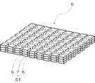
さらに、セラミック焼結積層体5をライン状に分割した方向と直交する方向にブレード8を移動させて、図9に示すように、セラミック焼結積層体5全体を複数に個片化することができる。なお、第1焼結基板6が個片化されたセラミック基板1を第1セラミック基板9とし、第2焼結基板7が個片化されたセラミック基板1を第2セラミック基板10とする。
Further, by moving the
図9では、セラミック焼結積層体5全体が複数に個片化されて、ブロック体51が複数形成される。ブロック体の1つは、ブロック体51の最上層および最下層が第1セラミック基板9であって、ブロック体51の中間層が第2セラミック基板10である。
In FIG. 9, the whole ceramic
ここでは、セラミック焼結積層体5を複数の個片に分割する工程において、第1収縮溝L10または第2収縮溝L20に沿って第1焼結基板6および第2焼結基板7を切断して、第1焼結基板6および第2焼結基板7のうちどちらか一方を個片に分割するとともに、第1焼結基板6および第2焼結基板7のうちどちらか他方を個片に分割することができる。このように、セラミック焼結積層体5を個片化するときは、第1焼結基板6および第2焼結基板7の両方をほぼ同時に個片にすることができ、図10に示したセラミック基板1の製造工程を単純化することができる。
Here, in the step of dividing the ceramic
本実施形態に係るセラミック基板の製造方法によれば、一度に同一種類のセラミック基板を多数製作することができる。また、複数の種類のセラミック基板を多数作製することができ、製造歩留まりを効果的に向上させることができる。 According to the method for manufacturing a ceramic substrate according to this embodiment, a large number of ceramic substrates of the same type can be manufactured at a time. In addition, a large number of ceramic substrates of a plurality of types can be manufactured, and the manufacturing yield can be effectively improved.
なお、本発明は上述の形態に限定されるものではなく、本発明の要旨を逸脱しない範囲において種々の変更、改良等が可能である。 In addition, this invention is not limited to the above-mentioned form, A various change, improvement, etc. are possible in the range which does not deviate from the summary of this invention.
ここでは、第1未焼結基板2を一例に説明するが、例えば、図11に示すように、マトリック状に形成される第1溝L1を第1未焼結基板2の上面および下面の両方に形成したものを用いてもよい。第1未焼結基板2の上面および下面に形成された第1溝L1は、平面視したときに、上面の溝と下面の溝が重なるように形成する。そして、同様に、第2未焼結基板3についても、第2未焼結基板3の上面および下面に同様の溝を形成する。そして、両未焼結基板を重ね合わせた未焼結積層体4を用いる。第1未焼結基板2および第2未焼結基板3の上面および下面に溝を形成しておくことで、セラミック焼結積層体5を個片化するときに、切断が容易となり、作製するセラミック基板1の形状を所望する形状に整えることができる。
Here, the first
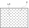
また、第1未焼結基板2に形成する溝を、図12に示すように、マトリック状に配列された不連続の貫通溝L3としてもよい。貫通溝L3とすることで、焼成時の熱収縮に起因する応力を貫通溝L3に逃がすことができ、セラミック焼結積層体5にクラックが発生するのを抑制することができる。
Further, the grooves formed in the first
また、第1未焼結基板2の個々の個片化領域の上に、第2未焼結基板3の個辺化領域をグリーンシートより打ち抜くとともに積層する。さらに、積層された第2未焼結基板3の個片化領域の上に、第1未焼結基板2の個片化領域を積層した未焼結焼結体4を準備することにより、焼成時の熱収縮に起因する応力を小さくすることができる。
In addition, the individual areas of the second
このようにして未焼結積層体4の未焼結基板同士の接触面積を減らすことができ、セラミック基板にするときに、異種セラミック材料の積層体である個々のセラミック積層体の面積が小さいことにより、積層体の積層界面に生じる応力が小さくなり、積層界面に生じるクラックまたは剥離といった不都合が発生するのを低減することができ、製造歩留まりを向上させることができる。
In this way, the contact area between the unsintered substrates of the
1 セラミック基板
2 第1未焼結基板
3 第2未焼結基板
4 未焼結積層体
5 セラミック焼結積層体
51 ブロック体
6 第1焼結基板
7 第2焼結基板
8 ブレード
9 第1セラミック基板
10 第2セラミック基板
L1 第1溝
L2 第2溝
L3 貫通溝
L10 第1収縮溝
L20 第2収縮溝
DESCRIPTION OF
Claims (5)
前記未焼結積層体を焼成して、前記第1溝および前記第2溝が収縮した第1収縮溝および第2収縮溝を有するセラミック焼結積層体を形成する工程と、
前記収縮溝に沿って前記セラミック焼結積層体を複数の個片に分割する工程と、を備えたセラミック基板の製造方法。 The first unsintered substrate made of a first ceramic material having first grooves formed in a matrix when viewed in plan, and the second grooves formed in a matrix when viewed in plan. A step of preparing an unsintered laminated body including a second unsintered substrate made of a second ceramic material different from the ceramic material and laminated so that the first groove and the second groove overlap in plan view When,
Firing the green laminate and forming a ceramic sintered laminate having a first shrinkage groove and a second shrinkage groove in which the first groove and the second groove shrink;
Dividing the ceramic sintered laminate into a plurality of pieces along the shrinkage grooves.
前記セラミック焼結積層体を、平面視したときに前記第1未焼結基板が焼結した第1焼結基板の前記第1収縮溝と、前記第2未焼結基板が焼結した第2焼結基板の前記第2収縮溝とが重なるように焼成することを特徴とするセラミック基板の製造方法。 A method for producing a ceramic substrate according to claim 1,
When the ceramic sintered laminate is viewed in plan, the first shrinkage groove of the first sintered substrate sintered by the first unsintered substrate, and the second sintered by the second unsintered substrate. A method for producing a ceramic substrate, comprising firing so that the second shrinkage groove of the sintered substrate overlaps.
前記セラミック焼結積層体を複数の個片に分割する工程において、前記第1収縮溝または前記第2収縮溝に沿って前記第1焼結基板および前記第2焼結基板を切断して、前記第1焼結基板および前記第2焼結基板を個片に分割することを特徴とするセラミック基板の製造方法。 A method for producing a ceramic substrate according to claim 2,
In the step of dividing the ceramic sintered laminate into a plurality of pieces, cutting the first sintered substrate and the second sintered substrate along the first shrinkage groove or the second shrinkage groove, A method of manufacturing a ceramic substrate, wherein the first sintered substrate and the second sintered substrate are divided into individual pieces.
前記未焼結積層体を少なくとも3層構造として、前記第1未焼結基板と前記第2未焼結基板とを交互に積層することを特徴とするセラミック基板の製造方法。 A method for producing a ceramic substrate according to claim 1,
A method for manufacturing a ceramic substrate, wherein the unsintered laminated body has at least a three-layer structure, and the first unsintered substrate and the second unsintered substrate are alternately stacked.
平面視したときにマトリックス状に形成された第2収縮溝を有する、前記第1セラミック材料と異なる第2セラミック材料からなる第2焼結基板とを含み、
平面視して前記第1焼結基板の前記第1収縮溝と前記第2焼結基板の前記第2収縮溝とが重なるようにして積層されている、ことを特徴とするセラミック焼結積層体。 A first sintered substrate made of a first ceramic material having first shrink grooves formed in a matrix when viewed in plan;
A second sintered substrate made of a second ceramic material different from the first ceramic material, having second contraction grooves formed in a matrix when viewed in plan,
A ceramic sintered laminate characterized in that the first shrinkage groove of the first sintered substrate and the second shrinkage groove of the second sintered substrate are laminated so as to overlap in plan view. .
Priority Applications (1)
| Application Number | Priority Date | Filing Date | Title |
|---|---|---|---|
| JP2011000484A JP2012142483A (en) | 2011-01-05 | 2011-01-05 | Ceramic substrate manufacturing method and ceramic sintered laminate |
Applications Claiming Priority (1)
| Application Number | Priority Date | Filing Date | Title |
|---|---|---|---|
| JP2011000484A JP2012142483A (en) | 2011-01-05 | 2011-01-05 | Ceramic substrate manufacturing method and ceramic sintered laminate |
Publications (1)
| Publication Number | Publication Date |
|---|---|
| JP2012142483A true JP2012142483A (en) | 2012-07-26 |
Family
ID=46678444
Family Applications (1)
| Application Number | Title | Priority Date | Filing Date |
|---|---|---|---|
| JP2011000484A Pending JP2012142483A (en) | 2011-01-05 | 2011-01-05 | Ceramic substrate manufacturing method and ceramic sintered laminate |
Country Status (1)
| Country | Link |
|---|---|
| JP (1) | JP2012142483A (en) |
Cited By (4)
| Publication number | Priority date | Publication date | Assignee | Title |
|---|---|---|---|---|
| CN103779200A (en) * | 2012-10-25 | 2014-05-07 | 三星钻石工业股份有限公司 | Breaking method for lamination ceramic substrate |
| JP2014083808A (en) * | 2012-10-25 | 2014-05-12 | Mitsuboshi Diamond Industrial Co Ltd | Method of segmenting laminated ceramic substrate |
| JP2014083798A (en) * | 2012-10-25 | 2014-05-12 | Mitsuboshi Diamond Industrial Co Ltd | Method of segmenting laminated ceramic substrate |
| CN104339461A (en) * | 2013-08-09 | 2015-02-11 | 三星钻石工业股份有限公司 | Method for cutting off laminated ceramic substrate |
-
2011
- 2011-01-05 JP JP2011000484A patent/JP2012142483A/en active Pending
Cited By (6)
| Publication number | Priority date | Publication date | Assignee | Title |
|---|---|---|---|---|
| CN103779200A (en) * | 2012-10-25 | 2014-05-07 | 三星钻石工业股份有限公司 | Breaking method for lamination ceramic substrate |
| JP2014083808A (en) * | 2012-10-25 | 2014-05-12 | Mitsuboshi Diamond Industrial Co Ltd | Method of segmenting laminated ceramic substrate |
| JP2014083798A (en) * | 2012-10-25 | 2014-05-12 | Mitsuboshi Diamond Industrial Co Ltd | Method of segmenting laminated ceramic substrate |
| TWI583522B (en) * | 2012-10-25 | 2017-05-21 | 三星鑽石工業股份有限公司 | Disassembly method of laminated ceramic substrate |
| CN104339461A (en) * | 2013-08-09 | 2015-02-11 | 三星钻石工业股份有限公司 | Method for cutting off laminated ceramic substrate |
| CN104339461B (en) * | 2013-08-09 | 2017-09-29 | 三星钻石工业股份有限公司 | The cutting-off method of laminated ceramic substrate |
Similar Documents
| Publication | Publication Date | Title |
|---|---|---|
| US7569177B2 (en) | Method of producing ceramic multilayer substrates, and green composite laminate | |
| US20150028988A1 (en) | Laminated coil | |
| WO2015129340A1 (en) | Ceramic substrate and method for manufacturing module product | |
| JP2012142483A (en) | Ceramic substrate manufacturing method and ceramic sintered laminate | |
| JP4821855B2 (en) | Multilayer ceramic substrate and manufacturing method thereof | |
| TW200308193A (en) | Ceramic multilayer substrate manufacturing method and un-sintered composite multilayer body | |
| JP5131349B2 (en) | Manufacturing method of multilayer piezoelectric ceramic element | |
| JP4788410B2 (en) | Manufacturing method of ceramic laminated substrate | |
| JP2016219691A (en) | Manufacturing method for multilayer ceramic electronic component | |
| JP2015076452A (en) | Method for manufacturing capacitor element | |
| WO2012144114A1 (en) | Wiring board, multi-pattern wiring board, and method for producing same | |
| JP5527048B2 (en) | Ceramic multilayer substrate | |
| WO2010007878A1 (en) | Multilayer ceramic substrate and method for manufacturing the same | |
| JP2004034448A (en) | Method for manufacturing multi-layer ceramic substrate | |
| JP5444593B2 (en) | Multilayer piezoelectric element | |
| JP2008159725A (en) | Ceramic multi-layered substrate, and its manufacturing method | |
| CN103700764A (en) | Method for manufacturing piezoelectric element comprising HfO2 stress buffer body | |
| JP6119843B2 (en) | Method for manufacturing multilayer inductor element, multilayer inductor element, and multilayer body | |
| JP2011018783A (en) | Method of manufacturing multilayer ceramic substrate | |
| JP2012004422A (en) | Ceramic multilayer substrate | |
| JP7182780B2 (en) | Method for manufacturing multilayer ceramic chip and method for manufacturing pre-fired chip for manufacturing multilayer ceramic chip | |
| JP5293471B2 (en) | Manufacturing method of electronic parts | |
| JP2009200404A (en) | Method of manufacturing ceramic wiring board | |
| JP2009170752A (en) | Electronic component | |
| JP2011258681A (en) | Laminated piezoelectric actuator and manufacturing method therefor |