JP2012114467A - Substrate production method and electronic component mounting apparatus - Google Patents
Substrate production method and electronic component mounting apparatus Download PDFInfo
- Publication number
- JP2012114467A JP2012114467A JP2012053407A JP2012053407A JP2012114467A JP 2012114467 A JP2012114467 A JP 2012114467A JP 2012053407 A JP2012053407 A JP 2012053407A JP 2012053407 A JP2012053407 A JP 2012053407A JP 2012114467 A JP2012114467 A JP 2012114467A
- Authority
- JP
- Japan
- Prior art keywords
- substrate
- lane
- production
- board
- priority
- Prior art date
- Legal status (The legal status is an assumption and is not a legal conclusion. Google has not performed a legal analysis and makes no representation as to the accuracy of the status listed.)
- Granted
Links
- 239000000758 substrate Substances 0.000 title claims abstract description 205
- 238000004519 manufacturing process Methods 0.000 title claims abstract description 107
- 230000032258 transport Effects 0.000 description 54
- 238000001514 detection method Methods 0.000 description 11
- 230000000694 effects Effects 0.000 description 3
- 230000007246 mechanism Effects 0.000 description 2
- 241000894007 species Species 0.000 description 2
- 238000011144 upstream manufacturing Methods 0.000 description 2
- 241000257465 Echinoidea Species 0.000 description 1
- 230000008901 benefit Effects 0.000 description 1
- 230000008859 change Effects 0.000 description 1
- 230000007547 defect Effects 0.000 description 1
- 230000006866 deterioration Effects 0.000 description 1
- 230000012447 hatching Effects 0.000 description 1
- 230000006872 improvement Effects 0.000 description 1
- 238000000034 method Methods 0.000 description 1
- 230000004048 modification Effects 0.000 description 1
- 238000012986 modification Methods 0.000 description 1
- 230000008569 process Effects 0.000 description 1
Images


Classifications
-
- Y—GENERAL TAGGING OF NEW TECHNOLOGICAL DEVELOPMENTS; GENERAL TAGGING OF CROSS-SECTIONAL TECHNOLOGIES SPANNING OVER SEVERAL SECTIONS OF THE IPC; TECHNICAL SUBJECTS COVERED BY FORMER USPC CROSS-REFERENCE ART COLLECTIONS [XRACs] AND DIGESTS
- Y02—TECHNOLOGIES OR APPLICATIONS FOR MITIGATION OR ADAPTATION AGAINST CLIMATE CHANGE
- Y02P—CLIMATE CHANGE MITIGATION TECHNOLOGIES IN THE PRODUCTION OR PROCESSING OF GOODS
- Y02P90/00—Enabling technologies with a potential contribution to greenhouse gas [GHG] emissions mitigation
- Y02P90/02—Total factory control, e.g. smart factories, flexible manufacturing systems [FMS] or integrated manufacturing systems [IMS]
Landscapes
- General Factory Administration (AREA)
- Supply And Installment Of Electrical Components (AREA)
Abstract
Description
本発明は、複数の基板搬送レーンに基板を流し、優先レーンの基板に対して電子部品を装着するようにした基板生産方法および電子部品実装装置に関するものである。 The present invention relates to a substrate production method and an electronic component mounting apparatus in which a substrate is made to flow through a plurality of substrate transfer lanes and electronic components are mounted on substrates in a priority lane.
製品履歴の追跡を正しく行うことができるように、生産ロットにおける基板の搬送順序を先入れ・先出しの原則通りに維持できるようにした電子部品実装装置は、例えば、特許文献1に記載されている。 For example, Patent Document 1 discloses an electronic component mounting apparatus that can maintain a board transportation order in a production lot according to a first-in first-out principle so that product history can be tracked correctly. .
特許文献1に記載されたものは、実装対象の基板に、生産ロットにおける搬送順序を示す追番号Nを付与し、追番号Nが偶数であるか、奇数であるかによって、2列の待機ステージの何れかに搬入するようにしている。すなわち、基板を2つの搬送路に交互に供給し、未実装基板を待機する待機ステージより実装ステージへ、および実装ステージより実装済基板を待機する待機ステージへ基板を移動させる際に、2つの搬送路上の基板の追番号の大小比較を行い、小さい追番号の基板を先行して移動させるように基板の移動順序を決定するようにしている。これによって、上流側から搬入された順序に従って、先入れ、先出しの原則が維持される。この結果、特許文献1に記載のものによれば、不具合発生時の製品履歴の追跡を容易に行うことができる利点がある。 The device described in Patent Document 1 assigns an additional number N indicating a transfer order in a production lot to a substrate to be mounted, and two rows of standby stages depending on whether the additional number N is an even number or an odd number. I carry it in either. That is, when the substrate is alternately supplied to the two transport paths, and the substrate is moved from the standby stage waiting for the unmounted substrate to the mounting stage, and from the mounting stage to the standby stage waiting for the mounted substrate, the two transports are performed. The sequence number of the substrates on the road is compared, and the movement order of the substrates is determined so that the substrate with the smaller sequence number is moved in advance. As a result, the principle of first-in and first-out is maintained according to the order of loading from the upstream side. As a result, according to the device described in Patent Document 1, there is an advantage that it is possible to easily track the product history when a problem occurs.
しかしながら、特許文献1に記載のものにおいては、カセットフィーダの部品切れ等により、一方の搬送路上の基板に電子部品を実装できなくなった場合の対応については、全く記載されておらず、一方の搬送路上の基板に部品切れ等の事態が発生した場合には、他方の搬送路における生産が可能であっても、運転を停止せざるを得ず、スループットが低下する問題がある。 However, in the case of the one described in Patent Document 1, there is no description about what to do when an electronic component cannot be mounted on the substrate on one of the conveyance paths due to a component cutout of the cassette feeder or the like. When a situation such as part shortage occurs on the substrate on the road, there is a problem that the throughput is reduced because the operation must be stopped even if the production on the other transport path is possible.
本発明は、上記した従来の不具合を解消するためになされたもので、部品切れ等によって優先レーンでの生産が継続できなくなった場合は、他の生産可能なレーンに生産を切替え、その後、優先レーンでの生産が可能となった場合に、優先レーンに生産復帰する基板生産方法および電子部品実装装置を提供することを目的とするものである。 The present invention has been made to solve the above-described conventional problems. When production in the priority lane cannot be continued due to a component shortage or the like, the production is switched to another production-capable lane, and then priority is given. It is an object of the present invention to provide a substrate production method and an electronic component mounting apparatus that return production to a priority lane when production in the lane becomes possible.
上記した課題を解決するために、請求項1に係る発明の特徴は、基板を搬送する複数の基板搬送レーンを有し、該複数の基板搬送レーン上を搬送される基板に電子部品を順次実装する電子部品実装装置における基板生産方法であって、実装される電子部品が異なる異種の基板を、前記複数の基板搬送レーンの各々に投入し、前記複数の基板搬送レーンのうち先に基板が投入された基板搬送レーンを優先レーンに設定し、該優先レーン上の基板に電子部品を実装し、優先レーン上の基板の生産が継続できなくなった場合には、他の生産可能な基板搬送レーン上の基板に電子部品を実装するように生産するレーンを切替え、その後、前記優先レーン上の基板の生産が継続できるようになった段階で、前記優先レーン上の基板に電子部品を実装するように生産復帰させるようにした基板生産方法である。 In order to solve the above-described problem, the invention according to claim 1 is characterized in that a plurality of substrate transport lanes for transporting a substrate are provided, and electronic components are sequentially mounted on the substrate transported on the plurality of substrate transport lanes. A board production method for an electronic component mounting apparatus , wherein different types of boards to be mounted are loaded into each of the plurality of board transfer lanes, and the board is loaded first among the plurality of board transfer lanes. If the board transportation lane is set as the priority lane, and electronic components are mounted on the board on the priority lane, and the production of the board on the priority lane cannot be continued, the board transportation lane that can be produced The lanes to be produced are switched so that the electronic components are mounted on the board of the same, and then the electronic parts are mounted on the boards on the priority lanes when the production of the boards on the priority lanes can be continued. A board production methods so as to urchin production restored.
請求項2に係る発明の特徴は、実装される電子部品が異なる異種の基板を各々搬送する複数の基板搬送レーンと、部品供給装置から電子部品をピックアップして前記基板搬送レーン上の基板に装着する装着手段と、前記複数の基板搬送レーンのうち先に基板が投入された基板搬送レーンを優先レーンに設定する優先レーン設定手段と、該優先レーン上の基板に電子部品を装着するように前記装着手段を制御するとともに、優先レーンに設定された基板搬送レーン上の基板の生産が継続できなくなった場合は、他の生産可能な基板搬送レーン上の基板に電子部品を装着するように生産するレーンを切替えるレーン切替え手段と、前記優先レーン上の基板の生産が継続できるようになった場合には前記優先レーン上の基板に電子部品を装着するように生産復帰させる生産復帰手段とを備えた電子部品実装装置である。
A feature of the invention according to
上記のように構成した請求項1、2に係る発明によれば、実装される電子部品が異なる異種の基板を、複数の基板搬送レーンの各々に投入するようになっているので、異種の基板は、複数の基板搬送レーンに投入した順序で、払い出しされるようになり、これによって、同一レーンより基板が連続して払い出されることによって発生するスループットのバランスのくずれを小さくできるようになり、バランスの取れたスループットを実現できる。
According to the invention according to
以下、本発明の実施の形態を図面に基づいて説明する。図1は、電子部品実装装置10の全体構成を概略的に示すもので、当該電子部品実装装置10は、主として、部品供給装置11、基板保持装置13、部品移載装置14、基板搬送装置15によって構成されている。なお、以下の説明においては、図1の左右方向をX軸、上下方向をY軸とする。
Hereinafter, embodiments of the present invention will be described with reference to the drawings. FIG. 1 schematically shows an overall configuration of an electronic
基板搬送装置15は、基板16を図1の左右方向(X軸方向)に搬送するもので、基板搬送装置15は、X軸方向に沿って配設された2列の基板搬送レーン17、18と、これら基板搬送レーン17、18に沿って基板16を搬送する図略のベルトコンベアを備えている。2列の基板搬送レーン17、18は、基台20の中央部に配設された一対の実装ステージ17a、18aを備えている。
The
各基板搬送レーン17、18に搬入された基板16は、図略のベルトコンベアによって実装ステージ17a、18aに搬入され、これら実装ステージ17a、18aに搬送された基板16は、基板保持装置13に設けられた図略のクランプ装置によって位置決めクランプされ、その状態で、基板16上に電子部品が装着される。基板16に電子部品が装着されると、基板16は図略のベルトコンベアによって実装ステージ17a、18aより払い出される。
The
なお、実装ステージ17a、18aには、これら実装ステージ17a、18aに搬送された基板16を検出する基板検出センサS1、S2がそれぞれ設置されている。基板検出センサS1、S2の信号は、後述する制御装置に送出され、この制御装置によって、基板搬送レーン17、18上に実装ステージ17a、18aに搬送する基板16が存在し、実装ステージ17a、18aに基板16が存在せず空きの状態である場合に、基板搬送装置15に基板16の搬送が指令されるようになっている。
The
部品移載装置14は、図1の上下方向(Y軸方向)に移動可能なY軸スライド21と、このY軸スライド21に図1の左右方向(X軸方向)に移動可能に支持されたX軸スライド22を備えている。Y軸スライド21は、図略のボールねじ機構を介してY軸サーボモータによりY軸方向に移動されるようになっており、また、X軸スライド22は、図略のボールねじ機構を介してX軸方向に移動されるようになっている。X軸スライド22には、電子部品を吸着保持する吸着ノズルを備えた装着ヘッド23が取付けられている。装着ヘッド23は、吸着ノズルに吸着保持した電子部品を基板16に装着するものである。
The
また、基台20上には、装着ヘッド23に保持された電子部品の保持状態を撮像するCCDカメラ24が取付けられ、CCDカメラ24で撮像したデータに基づいて、電子部品の有無の確認および吸着保持の良否を判別できるようにしている。
Further, a
部品供給装置11は、複数のカセット式フィーダ25からなり、これらカセット式フィーダ25は、基板搬送レーン17、18の外側に、交換可能にX軸方向に並設されている。各カセット式フィーダ25のテープには、それぞれ電子部品が一定のピッチ間隔に収納保持され、テープをモータ等によりピッチ送りすることにより、電子部品を所定位置に供給するようになっている。
The
図2において、30は、電子部品実装装置10を制御する制御装置を示し、当該制御装置30は、中央処理装置(CPU)と、各種の制御データおよび制御プログラム等を記憶するメモリと、入出力装置からなっており、制御装置30によって、基板16の搬送や、基板16への電子部品の実装が制御されるようになっている。制御装置30は、優先レーン設定手段31、生産レーン切替え手段32および生産レーン復帰手段33を備えている。
In FIG. 2,
優先レーン設定手段31は、複数の基板搬送レーン17、18のうち、実装ステージ17a、18aに先に基板16が投入された基板搬送レーンを優先レーンに設定するものであり、優先レーンに設定された基板搬送レーン上の基板16に対して電子部品の実装作業が実行される。
The priority lane setting means 31 sets the substrate transport lane in which the
生産レーン切替え手段32は、優先レーンに設定された基板搬送レーン上の基板16の実装作業が、部品切れ等の理由によって継続できなくなった場合に、もう一方の基板搬送レーン(非優先レーン)上に電子部品の実装作業が行える基板16が存在していることを条件に、電子部品の実装作業を非優先レーンに切替えるものである。これによって、優先レーンでの生産が継続できなくなった間においても、実装作業を中断することなく継続して行えるようにしている。
The production lane switching means 32 is provided on the other board transfer lane (non-priority lane) when the mounting operation of the
生産レーン復帰手段33は、例えば、部品切れを生じたカセット式フィーダ25がセット(補給)され、優先レーンでの生産が可能となった場合に、非優先レーン上の基板16の実装作業を中断して、再び優先レーン上の基板16の実装作業に復帰させるものである。これによって、基板16を投入された順番に払い出すことができるようになる。
The production lane return means 33, for example, interrupts the mounting operation of the
制御装置30には、基板16を搬送する基板搬送装置15と、装着ヘッド23を取付けたX軸、Y軸スライド22、21を駆動するスライド駆動装置35と、カセット式フィーダ25の部品切れを検出する部品切れ検出装置36と、基板検出センサS1、S2がそれぞれ接続されている。なお、部品切れ検出装置36は、装着ヘッド23の吸着ノズルに電子部品が吸着されなくなったことを検出するCCDカメラ24によって構成することができる。あるいはまた、カセット式フィーダ25に収納保持された電子部品の残量を管理することによって、部品切れを検出することもできる。
The
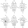
次に、図3を参照しながら、基板16の実装制御について説明する。なお、以下の説明においては、2列の基板搬送レーン17、18に同種の基板16を投入し、1つの装着ヘッド23によって各基板搬送レーン17、18上の基板16に電子部品を順次実装する実施例について述べる。
Next, the mounting control of the
2列の基板搬送レーン17、18に基板16がない状態で、図3(A)に示すように、2列の基板搬送レーン17、18の何れか一方、例えば、第1の基板搬送レーン17に、電子部品を実装すべき基板16(図3(A)2点鎖線)が搬入される。
As shown in FIG. 3A, in the state where the
第1の基板搬送レーン17に基板16が搬入され、かつ実装ステージ17aにおいて基板の空き状態が基板検出センサS1の信号に基づいて検出されると、第1の基板搬送レーン17に搬入された基板16は、図3(A)の実線で示すように、図略のベルトコンベアによって実装ステージ17aに搬入され、図略のクランプ装置によって位置決めクランプされる。そして、制御装置30の優先レーン設定手段31によって、実装ステージ17aに先に基板16が搬送された基板搬送レーン17が、優先レーンと設定される。
When the
実装ステージ17aに基板16が搬送されると、XY軸スライド駆動装置35が作動され、装着ヘッド23の吸着ノズルによってカセット式フィーダ25より電子部品が吸着保持されて、図3(B)に示すように、優先レーンに設定された基板搬送レーン17の実装ステージ17a上の基板16に対して電子部品の実装作業が実行される。なお、2列の基板搬送レーン17、18の実装ステージ17a、18aに同時に基板16が搬入された場合には、予め定められた特定の基板搬送レーン(例えば、第1の基板搬送レーン17)が優先レーンと定められる。
When the
ところで、実装ステージ17aにおいて、電子部品を実装している最中に、図3(C)に示すように、あるカセット式フィーダ25に部品切れが発生すると、これが部品切れ検出装置36によって検出され、制御装置30に対して部品切れ信号が送出される。これにより、優先レーンでの生産継続が不可能な状態になったことが認識され、実装ステージ17aにおける基板16への電子部品の実装作業が中断される。なお、図3(C)において、部品切れを生じたカセット式フィーダ25、および実装作業を中断した基板16をそれぞれ網かけして示している。
By the way, in the mounting
部品切れにより、優先レーンでの生産継続が不可能な状態になったことが検出されると、優先レーンではないもう一方の基板搬送レーン18(以下、これを非優先レーンという)の実装ステージ18aに、生産可能な基板16が存在するか否かを確認される。図3(C)に示すように、非優先レーンの実装ステージ18aに、生産可能な基板16が存在する場合には、制御装置30の生産レーン切替え手段32によって、生産レーンの切替えが指令され、装着ヘッド23によって電子部品を実装するレーンを基板搬送レーン18側に切替えて生産を開始する。
When it is detected that production cannot be continued in the priority lane due to out of parts, the mounting
すなわち、スライド駆動装置35を制御して、装着ヘッド23を、非優先レーンの実装ステージ18aとカセット式フィーダ25との間で作動させ、図3(D)に示すように、非優先レーンの実装ステージ18aに位置決めクランプされている基板16に対して電子部品を実装する。この場合、ある電子部品に部品切れが発生しているため、当該電子部品を除いた実装作業となり、非優先レーンで実装作業が完了されることはない。この間に、作業者によって部品切れを生じたカセット式フィーダ25の交換作業が行われる。
That is, by controlling the
非優先レーンにおける基板16への電子部品の実装作業中に、部品切れを生じたカセット式フィーダ25の交換が完了し、図3(E)に示すように、優先レーンにおける生産を継続できる条件が整うと、制御装置30の生産レーン復帰手段33によって、生産レーンの復帰が指令され、この指令に基づいて、非優先レーンにおける実装作業を中断し、再び優先レーン(基板搬送レーン17)における生産を再開する。
During the mounting operation of the electronic component on the
このようにして、優先レーンにおける基板16への電子部品の所定の実装作業が完了すると、図3(F)に示すように、所定の実装作業が完了した基板16が図略のベルトコンベアによって、実装ステージ17aから搬出されるとともに、実装作業を中断していた非優先レーンにおける基板16への実装作業が再開される。その後、非優先レーンにおける基板16への電子部品の所定の実装作業が完了すると、当該基板16が図略のベルトコンベアによって、実装ステージ18aから搬出される。
In this way, when the predetermined mounting operation of the electronic components on the
この結果、基板16は、基板搬送レーン17、18に投入した順序で、払い出しできるようになり、これによって、例えば、基板に不具合が発生した場合においても、簡易のトレーサビリティ管理、すなわち、製品履歴の追跡を容易に行えるようになる。
As a result, the
しかも、上記した実施の形態によれば、優先レーン上の基板16に電子部品が供給できなくなった場合においても、生産を停止させることなく継続できるので、基板16を生産する稼働率を向上することができるとともに、基本的に基板搬送レーン17、18に投入された順序で基板16を払い出すことができるため、スループットのバランスのくずれを小さくでき、スループットの低下を抑えることができる。
Moreover, according to the above-described embodiment, even when electronic components cannot be supplied to the
上記した実装制御においては、2列の基板搬送レーン17、18に同種の基板16を投入する例で説明したが、2列の基板搬送レーン17、18に異種の基板16、すなわち、実装すべき電子部品を異にする基板16を投入することもでき、この実施例を図4に基づいて説明する。なお、以下においては、第1の基板搬送レーン17に投入される基板を、16Aと表わし、第2の基板搬送レーン18に投入される基板を、16Bと表わすことにする。
In the above-described mounting control, the example in which the same type of
図4(A)〜(D)は、図3(A)〜(D)に基づいて述べたと同様に、優先レーン(第1の基板搬送レーン17)において、電子部品を実装している最中に、あるカセット式フィーダ25に部品切れが発生して、優先レーンでの生産継続が不可能な状態になった場合には、非優先レーン(第2の基板搬送レーン18)の実装ステージ18aに、生産可能な基板16が存在することを条件にして、実装作業が優先レーンから非優先レーンに切替えられる。
4A to 4D are similar to those described with reference to FIGS. 3A to 3D, while electronic components are being mounted in the priority lane (first substrate transfer lane 17). In addition, when a part of the
ところが、優先レーンと非優先レーンを異種の基板16A、16Bが流れているため、部品切れを生じた電子部品の種類によっては、非優先レーンにおける基板16Bの実装作業には使用しない場合がある。その結果、非優先レーンにおける基板16Bの実装作業時間によっては、部品切れの電子部品が補給される前に、非優先レーンにおける基板16Bへの電子部品の実装作業が完了してしまうことが発生する。
However, since different types of
従って、この実施例のように、優先レーンにおける生産を再開できる条件が整う前に、非優先レーンにおける基板16Bへの電子部品の実装作業が完了した場合には、図4(E)に示すように、非優先レーン上の実装済基板16Bを、図略のベルトコンベアによって、実装ステージ18aから搬出するように制御する。
Accordingly, as shown in FIG. 4E, when the mounting operation of the electronic components on the
そして、図4(F)に示すように、部品切れしたカセット式フィーダ25が補給され、優先レーンにおける生産を継続できる条件が整うと、制御装置30の生産レーン復帰手段33によって、生産レーンの復帰が指令され、この指令に基づいて、優先レーンにおける生産が再開される。そして、優先レーンにおける基板16Aの所定の実装作業が完了すると、当該基板16Aは実装ステージ17aから搬出される。
Then, as shown in FIG. 4F, when the
このように、第1および第2の基板搬送レーン17、18に異種の基板16A、16Bを投入する場合においては、カセット式フィーダ25の交換に要する時間と、非優先レーン上の基板16Bの実装時間との関係で、稀に、基板搬送レーン17、18に投入した順序で基板16を払い出しすることができなくなる恐れが発生するが、基本的には、基板搬送レーン17、18に投入した順序で、基板16の払い出しが行われることになる。これにより、スループットのバランスのくずれを小さくでき、スループットの低下を抑えることができる。
As described above, when different types of
図5は、図4で述べた実施例の変形例を示すもので、異種の基板16A、16Bを生産する場合においても、非優先レーンの基板を先に払い出すことがないようにして、必ず基板搬送レーン17、18に投入した順序で、基板16の払い出しが行われるようにしたものである。
FIG. 5 shows a modification of the embodiment described with reference to FIG. 4. Even when different types of
すなわち、図4で述べた実施例と同様に、電子部品を実装すべき基板16が、第1および第2の基板搬送レーン17、18の何れか一方の実装ステージ(例えば、第1の基板搬送レーン17の実装ステージ17a)に搬入される(図5(A)参照)と、優先レーン設定手段31によって第1の基板搬送レーン17が優先レーンに設定される。
That is, as in the embodiment described with reference to FIG. 4, the
実装ステージ17aに基板16Aが搬送されると、図5(B)に示すように、実装ステージ17a上の基板16Aに電子部品が実装される。そして、電子部品を実装している最中に、図5(C)に示すように、あるカセット式フィーダ25に部品切れが発生すると、部品切れ検出装置36の検出信号に基づいて、実装ステージ17aにおける基板16Aへの電子部品の実装作業が中断されるとともに、生産レーン切替え手段32によって、生産レーンの切替えが指令される。これによって、図5(D)に示すように、非優先レーンの実装ステージ18aに位置決めクランプされている基板16Bに対して電子部品が実装される。
When the
この場合、優先レーンと非優先レーンを異種の基板16A、16Bが流れているため、部品切れを生じたカセット式フィーダ25が補給される前に、非優先レーンにおける基板16Bへの電子部品の実装作業がすべて完了してしまうことが発生する。しかしながら、予め優先レーンにおける基板16Aを必ず先に払い出すように設定しておくことにより、非優先レーンにおいて電子部品の実装作業が完了した基板16Bは、払い出されることなく、その状態で待機する。このときの基板16Bを図5(F)に斜線入りで示している。
In this case, since the different types of
しかる状態で、カセット式フィーダ25が補給され、優先レーンにおける生産を継続できる条件が整うと、図5(F)に示すように、再び優先レーンにおける生産を開始するように復帰される。このようにして、優先レーンにおける基板16Aへの電子部品の実装作業が完了すると、図5(G)に示すように、優先レーン上の基板16Aが図略のベルトコンベアによって、実装ステージ17aから搬出される。
In this state, when the cassette-
そして、優先レーン上の基板16Aの払い出しが完了した後に、非優先レーンの実装ステージ18aに基板16Bが存在している場合には、非優先レーンであった第2の基板搬送レーン18が、今度は優先レーンに切替えられる。このとき、優先レーン(第2の基板搬送レーン18)上に払い出すべき実装済の基板16Bが存在しているため、当該基板16Bが、図略のベルトコンベアによって、実装ステージ18aから搬出される。
When the
これによって、異種の基板16A、16Bは、2列の基板搬送レーン17、18に投入した順序で、払い出しされるようになり、これによって、いかなる状況下においても、同一レーンより基板が連続して払い出されることによって発生するスループットのバランスのくずれを防止できるようになり、バランスの取れた理想通りのスループットを実現できる。同時に、不具合発生時の製品履歴の追跡も行えるようになる。
As a result, the different types of
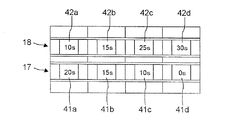
図6は、2列の基板搬送レーン17、18上に、それぞれ複数の実装ステージ41a、42a〜41d、42dを配設し、各実装ステージ41a、42a〜41d、42dにおいて、異種の基板16A、16Bを順次生産する例を示したものであり、これをもとに上記した実施の形態の生産方法を適用した場合の効果を詳しく説明する。
In FIG. 6, a plurality of mounting
このようなライン構成においては、各基板搬送レーン17、18における複数の実装ステージ41a、42a〜41d、42dにおける生産時間は必ずしも一致しない。ここで、基板を第1および第2の基板搬送レーン17、18に交互に投入して、順番に生産するものとすると、その生産ラインにおけるスループットは、第1および第2の基板搬送レーン17、18の生産時間を足したものとなる。そして、生産ラインのスループットは、生産ライン内で最も時間がかかる実装ステージによって決まるため、予め、2つのレーン17、18の生産時間を足したものがほぼ等しくなるように、各実装ステージにおける生産時間のバランスをとっている。このために、各実装ステージ41a、42a〜41d、42dにおける生産時間を、例えば、図6に示すように割り振ることにより、生産ラインのスループットは第3の実装ステージによって決定される35秒となる。
In such a line configuration, the production times in the plurality of mounting
ところで、例えば、第1の基板搬送レーン17の2番目の実装ステージ41bにおいて、部品切れ等により生産継続が不可能になった場合、図3から図5の例で述べたように、生産レーンが第2の基板搬送レーン18の側に切替えられ、2番目の実装ステージ42bによって引き続き生産が継続されるようになる。
By the way, for example, in the
この場合、部品切れした部品が補給されても、第2の基板搬送レーン18の2番目の実装ステージ42bにおける基板の生産を、所定の実装作業が完了するまで継続すると、2番目の実装ステージから3番目の実装ステージに、連続して同じレーンから基板が流れることになる。このような現象は、特に、レーンを切替えた実装ステージにおける生産時間が短く、基板を短時間で後工程に払い出してしまう場合等により顕著に起こり得る。このために、3番目の実装ステージでの生産時間が変化(増加)することになり、ラインのスループットが一瞬悪化する結果を招く。すなわち、通常3番目の実装ステージにおいては、35秒で2つの基板が生産されていたものが、片側だけのレーン生産では、2つの基板を生産するのに50秒(25秒×2)を要することになる。
In this case, if the production of the substrate on the
しかしながら、本実施の形態で述べたように、優先レーン(第1の基板搬送レーン17)上の基板16Aに電子部品が供給できるようになった場合に、非優先レーン(第2の基板搬送レーン18)から優先レーン上の基板に電子部品を実装するように生産復帰させることにより、同じレーンの基板が連続して流れる可能性が減少できるようになる。これによって、1ライン当たりのスループット変化が最小限に抑えられ、ラインのスループット向上が期待できる。
However, as described in the present embodiment, when an electronic component can be supplied to the
なお、図6に示した例は実施の形態の生産方法を適用した場合の効果を説明するための一例であり、2列の基板搬送レーン17、18において同種の基板を生産する場合など、図6において各実装ステージ41a、42a〜41d、42dにおける生産時間が同じである場合であっても、スループットのバランスのくずれを小さくでき、スループットの低下を抑えることができる。この点を説明すると、通常のバランスが取れた状態では、一方の基板搬送レーンでの生産中にもう一方の基板搬送レーンの基板の搬入出を行うことができるため、基板搬送による生産のロスタイムは見かけ上ゼロとなるが、基板の搬入出の順序が変わると、その上流や下流の実装ステージにおいては一方の基板搬送レーンでの生産中にもう一方の基板搬送レーンの基板の搬入出を行うことができなくなり、そのような場合には基板の搬送時間がロスタイムとなってしまう。しかし、上記した実施の形態のごとく基本的に基板搬送レーン17、18に投入された順序で基板16を払い出すことができれば、通常のバランスが取れた状態を大きく崩すことがないため基板搬送による生産のロスタイムが生じにくくなるのである。
The example shown in FIG. 6 is an example for explaining the effect when the production method according to the embodiment is applied. For example, when the same kind of substrates are produced in the two rows of
上記した実施の形態においては、2列の基板搬送レーン17、18を設けた電子部品実装装置10について述べたが、基板搬送レーンは必ずしも2列に限定されるものではなく、基板搬送レーンを3列以上設けたものにも本発明は適用できるものである。
In the above-described embodiment, the electronic
また、上記した実施の形態においては、先に基板が投入された基板搬送レーンを優先レーンに設定したが、先に投入された基板を優先基板に設定し、この優先基板を先に払い出すように制御し、優先基板を払い出した後に、他のレーンの基板を払い出すようにすることもできる。この場合も、表現こそ違え、優先レーンを設定することと実質的に同じであることは明らかであり、従って、優先レーンを設定することと同意語と解釈されるべきものであり、その範疇に包含されることは勿論である。 Further, in the above-described embodiment, the substrate transport lane into which the substrate has been first input is set as the priority lane. However, the substrate that has been input first is set as the priority substrate, and this priority substrate is paid out first. It is also possible to pay out the boards in other lanes after paying out the priority board. In this case, too, it is clear that the expression is different and is substantially the same as setting the priority lane, so it should be construed as synonymous with setting the priority lane, and in that category Of course included.
また、上記した実施の形態においては、基板16に装着すべき電子部品の部品切れが生じたときに、生産するレーンを切替えるようにしたが、生産するレーンの切替えは、部品切れが生じた場合だけでなく、何らかの理由によって優先レーンでの生産の続行が困難になった場合、例えば、カセット式フィーダ25が故障した場合、画像処理にエラーが発生した場合、あるいは作為的に生産を一時的にストップする場合等の理由によって、基板の生産が継続できなくなった場合に適用できるものである。
Further, in the above-described embodiment, the production lane is switched when the electronic component to be mounted on the
なお、作為的に生産を一時的にストップする場合とは、例えば、部品供給装置11に空スロットが存在する場合に、カセット式フィーダ25の部品がなくなりそうになることを、残量管理によって検出して事前に警告を発し、この警告に基づいて作業者により、予め予備のカセット式フィーダを空スロットにセットすることによって生ずる。すなわち、カセット式フィーダ25の部品がなくなった場合、電子部品の取り出しを予備のカセット式フィーダから行うことにより、生産レーンを切替えなくても、部品切れによる生産の中断をなくすることが可能となるが、正規の部品取り出し位置において実装作業の効率が最適化されているため、予備のカセット式フィーダ25を、電子部品が無くなって取外された正規の部品取り出し位置にセットし直すことがあるためである。このように、優先レーン上の基板の生産が停止する時間がわずかな場合には、スループットのバランスのくずれがほとんどなく効果が大きくなる。
In addition, when the production is temporarily stopped temporarily, for example, when there is an empty slot in the
さらに、上記した実施の形態においては、2列の基板搬送レーン17、18の実装ステージにそれぞれ基板16を検出する基板検出センサS1、S2を設けた例について述べたが、これら基板検出センサを廃止し、基板搬送装置15を制御する制御装置30によって、各レーン上における基板16の位置を記憶させることも可能である。
Further, in the above-described embodiment, the example in which the substrate detection sensors S1 and S2 for detecting the
斯様に、上記した実施の形態で述べた具体的構成は、本発明の一例を示したものにすぎず、本発明はこのような具体的構成に限定されることなく、本発明の主旨を逸脱しない範囲で種々の態様を採り得るものである。 Thus, the specific configuration described in the above-described embodiment is merely an example of the present invention, and the present invention is not limited to such a specific configuration. Various embodiments can be adopted without departing from the scope.
10…電子部品実装装置、11…部品供給装置、13…基板保持装置、14…部品移載装置、15…基板搬送装置、16(16A、16B)…基板、17、18…基板搬送レーン、17a、18a…実装ステージ、21…Y軸スライド、22…X軸スライド、23…装着ヘッド、24…CCDカメラ、25…カセット式フィーダ、30…制御装置、31…優先レーン設定手段、32…生産レーン切替え手段、33…生産レーン復帰手段、35…スライド駆動装置、36…部品切れ検出装置、S1、S2…基板検出センサ。
DESCRIPTION OF
Claims (2)
実装される電子部品が異なる異種の基板を、前記複数の基板搬送レーンの各々に投入し、
前記複数の基板搬送レーンのうち先に基板が投入された基板搬送レーンを優先レーンに設定し、
該優先レーン上の基板に電子部品を実装し、
優先レーン上の基板の生産が継続できなくなった場合には、他の生産可能な基板搬送レーン上の基板に電子部品を実装するように生産するレーンを切替え、
その後、前記優先レーン上の基板の生産が継続できるようになった段階で、前記優先レーン上の基板に電子部品を実装するように生産復帰させるようにした、
ことを特徴とする基板生産方法。 A substrate production method in an electronic component mounting apparatus that has a plurality of substrate conveyance lanes for conveying a substrate and sequentially mounts electronic components on a substrate conveyed on the plurality of substrate conveyance lanes,
Putting different types of substrates with different electronic components into each of the plurality of substrate transfer lanes,
A substrate transport lane in which a substrate is first inserted among the plurality of substrate transport lanes is set as a priority lane,
Mount electronic components on the board on the priority lane,
When the production of the board on the priority lane cannot be continued, the production lane is switched so that the electronic component is mounted on the board on the other production board transportation lane,
After that, at the stage where the production of the board on the priority lane can be continued, the production is returned to mount the electronic component on the board on the priority lane.
A substrate production method characterized by the above.
部品供給装置から電子部品をピックアップして前記基板搬送レーン上の基板に装着する装着手段と、
前記複数の基板搬送レーンのうち先に基板が投入された基板搬送レーンを優先レーンに設定する優先レーン設定手段と、
該優先レーン上の基板に電子部品を装着するように前記装着手段を制御するとともに、優先レーンに設定された基板搬送レーン上の基板の生産が継続できなくなった場合は、他の生産可能な基板搬送レーン上の基板に電子部品を装着するように生産するレーンを切替えるレーン切替え手段と、
前記優先レーン上の基板の生産が継続できるようになった場合には前記優先レーン上の基板に電子部品を装着するように生産復帰させる生産復帰手段と、
を備えたことを特徴とする電子部品実装装置。 A plurality of substrate transport lanes for transporting different types of substrates with different electronic components to be mounted;
A mounting means for picking up an electronic component from a component supply device and mounting the electronic component on a substrate on the substrate transport lane;
Priority lane setting means for setting a substrate transport lane into which a substrate has been previously inserted among the plurality of substrate transport lanes as a priority lane;
When the mounting means is controlled to mount the electronic component on the substrate on the priority lane, and the production of the substrate on the substrate transport lane set as the priority lane cannot be continued, another substrate that can be produced Lane switching means for switching the lane to be produced so that electronic components are mounted on the substrate on the transfer lane,
When the production of the board on the priority lane can be continued, the production return means for returning the production so as to mount the electronic component on the board on the priority lane;
An electronic component mounting apparatus comprising:
Priority Applications (1)
| Application Number | Priority Date | Filing Date | Title |
|---|---|---|---|
| JP2012053407A JP5231666B2 (en) | 2012-03-09 | 2012-03-09 | Board production method and electronic component mounting apparatus |
Applications Claiming Priority (1)
| Application Number | Priority Date | Filing Date | Title |
|---|---|---|---|
| JP2012053407A JP5231666B2 (en) | 2012-03-09 | 2012-03-09 | Board production method and electronic component mounting apparatus |
Related Parent Applications (1)
| Application Number | Title | Priority Date | Filing Date |
|---|---|---|---|
| JP2007034687A Division JP4989250B2 (en) | 2007-02-15 | 2007-02-15 | Board production method and electronic component mounting apparatus |
Publications (2)
| Publication Number | Publication Date |
|---|---|
| JP2012114467A true JP2012114467A (en) | 2012-06-14 |
| JP5231666B2 JP5231666B2 (en) | 2013-07-10 |
Family
ID=46498268
Family Applications (1)
| Application Number | Title | Priority Date | Filing Date |
|---|---|---|---|
| JP2012053407A Active JP5231666B2 (en) | 2012-03-09 | 2012-03-09 | Board production method and electronic component mounting apparatus |
Country Status (1)
| Country | Link |
|---|---|
| JP (1) | JP5231666B2 (en) |
Cited By (1)
| Publication number | Priority date | Publication date | Assignee | Title |
|---|---|---|---|---|
| CN104584710A (en) * | 2012-08-24 | 2015-04-29 | 富士机械制造株式会社 | Optimization program and substrate processing system |
Citations (4)
| Publication number | Priority date | Publication date | Assignee | Title |
|---|---|---|---|---|
| JPH06252546A (en) * | 1993-02-23 | 1994-09-09 | Matsushita Electric Ind Co Ltd | Mounting-substrate production system |
| JP2003204192A (en) * | 2002-01-08 | 2003-07-18 | Matsushita Electric Ind Co Ltd | Apparatus and method for mounting electronic component |
| JP2008159855A (en) * | 2006-12-25 | 2008-07-10 | Hitachi High-Tech Instruments Co Ltd | Apparatus for mounting electronic component |
| JP2008186992A (en) * | 2007-01-30 | 2008-08-14 | Hitachi High-Tech Instruments Co Ltd | Electronic component mounting apparatus |
-
2012
- 2012-03-09 JP JP2012053407A patent/JP5231666B2/en active Active
Patent Citations (4)
| Publication number | Priority date | Publication date | Assignee | Title |
|---|---|---|---|---|
| JPH06252546A (en) * | 1993-02-23 | 1994-09-09 | Matsushita Electric Ind Co Ltd | Mounting-substrate production system |
| JP2003204192A (en) * | 2002-01-08 | 2003-07-18 | Matsushita Electric Ind Co Ltd | Apparatus and method for mounting electronic component |
| JP2008159855A (en) * | 2006-12-25 | 2008-07-10 | Hitachi High-Tech Instruments Co Ltd | Apparatus for mounting electronic component |
| JP2008186992A (en) * | 2007-01-30 | 2008-08-14 | Hitachi High-Tech Instruments Co Ltd | Electronic component mounting apparatus |
Cited By (3)
| Publication number | Priority date | Publication date | Assignee | Title |
|---|---|---|---|---|
| CN104584710A (en) * | 2012-08-24 | 2015-04-29 | 富士机械制造株式会社 | Optimization program and substrate processing system |
| JPWO2014030255A1 (en) * | 2012-08-24 | 2016-07-28 | 富士機械製造株式会社 | Optimization program and board-to-board work system |
| US9804592B2 (en) | 2012-08-24 | 2017-10-31 | Fuji Machine Mfg. Co., Ltd. | Optimization program and substrate process system |
Also Published As
| Publication number | Publication date |
|---|---|
| JP5231666B2 (en) | 2013-07-10 |
Similar Documents
| Publication | Publication Date | Title |
|---|---|---|
| JP4582181B2 (en) | Component mounting apparatus and manufacturing method of mounted products | |
| JP6319818B2 (en) | Method for managing board-to-board working system and mounting order of components of board-to-board working system | |
| JP4942497B2 (en) | Electronic component mounting device | |
| JP4346849B2 (en) | Electronic component mounting apparatus and electronic component mounting method | |
| JP2004119637A (en) | Electronic component mounting method and apparatus thereof, and electronic component mounting program | |
| US10863657B2 (en) | Electronic component mounting method | |
| JP4816472B2 (en) | Production management system, production management method and production management program in multiple production lines | |
| JP5293708B2 (en) | Electronic component mounting apparatus and electronic component mounting method | |
| WO2018011941A1 (en) | Component management system, component mounting device, and component managing method | |
| JP4989250B2 (en) | Board production method and electronic component mounting apparatus | |
| JP5231666B2 (en) | Board production method and electronic component mounting apparatus | |
| JP2011091288A (en) | Component mounting apparatus, and component mounting method | |
| JP2017011024A (en) | Electronic component mounting system | |
| JP5370204B2 (en) | Component mounting apparatus and component mounting method | |
| JP5375879B2 (en) | Electronic component mounting apparatus and board conveying method in electronic component mounting apparatus | |
| JP6277424B2 (en) | Component mounting apparatus and component mounting method | |
| JP2011171538A (en) | Component packaging apparatus and method of carrying substrate in apparatus | |
| JP5384764B2 (en) | Electronic component mounting method | |
| JP5321474B2 (en) | Component mounting apparatus and component mounting method | |
| JP5212399B2 (en) | Component mounting apparatus and board conveying method in component mounting apparatus | |
| JP5713799B2 (en) | Substrate conveyance control method and substrate conveyance control device for component mounting line | |
| JP7223180B2 (en) | production management system | |
| WO2023139644A1 (en) | Work machine system | |
| JP4692687B2 (en) | Mounting board manufacturing method | |
| JP7113188B2 (en) | Component supply device, component mounting system, and component mounting method |
Legal Events
| Date | Code | Title | Description |
|---|---|---|---|
| A621 | Written request for application examination |
Free format text: JAPANESE INTERMEDIATE CODE: A621 Effective date: 20120309 |
|
| TRDD | Decision of grant or rejection written | ||
| A01 | Written decision to grant a patent or to grant a registration (utility model) |
Free format text: JAPANESE INTERMEDIATE CODE: A01 Effective date: 20130312 |
|
| A977 | Report on retrieval |
Free format text: JAPANESE INTERMEDIATE CODE: A971007 Effective date: 20130314 |
|
| A61 | First payment of annual fees (during grant procedure) |
Free format text: JAPANESE INTERMEDIATE CODE: A61 Effective date: 20130321 |
|
| FPAY | Renewal fee payment (event date is renewal date of database) |
Free format text: PAYMENT UNTIL: 20160329 Year of fee payment: 3 |
|
| R150 | Certificate of patent or registration of utility model |
Ref document number: 5231666 Country of ref document: JP Free format text: JAPANESE INTERMEDIATE CODE: R150 Free format text: JAPANESE INTERMEDIATE CODE: R150 |
|
| R250 | Receipt of annual fees |
Free format text: JAPANESE INTERMEDIATE CODE: R250 |
|
| R250 | Receipt of annual fees |
Free format text: JAPANESE INTERMEDIATE CODE: R250 |
|
| R250 | Receipt of annual fees |
Free format text: JAPANESE INTERMEDIATE CODE: R250 |
|
| S533 | Written request for registration of change of name |
Free format text: JAPANESE INTERMEDIATE CODE: R313533 |
|
| R350 | Written notification of registration of transfer |
Free format text: JAPANESE INTERMEDIATE CODE: R350 |
|
| R250 | Receipt of annual fees |
Free format text: JAPANESE INTERMEDIATE CODE: R250 |
|
| R250 | Receipt of annual fees |
Free format text: JAPANESE INTERMEDIATE CODE: R250 |
|
| R250 | Receipt of annual fees |
Free format text: JAPANESE INTERMEDIATE CODE: R250 |
|
| R250 | Receipt of annual fees |
Free format text: JAPANESE INTERMEDIATE CODE: R250 |
|
| R250 | Receipt of annual fees |
Free format text: JAPANESE INTERMEDIATE CODE: R250 |
|
| R250 | Receipt of annual fees |
Free format text: JAPANESE INTERMEDIATE CODE: R250 |