JP2012109700A - Receiver, reception method, and electronic apparatus - Google Patents
Receiver, reception method, and electronic apparatus Download PDFInfo
- Publication number
- JP2012109700A JP2012109700A JP2010255569A JP2010255569A JP2012109700A JP 2012109700 A JP2012109700 A JP 2012109700A JP 2010255569 A JP2010255569 A JP 2010255569A JP 2010255569 A JP2010255569 A JP 2010255569A JP 2012109700 A JP2012109700 A JP 2012109700A
- Authority
- JP
- Japan
- Prior art keywords
- conversion
- signal
- modulation signal
- circuit
- detection method
- Prior art date
- Legal status (The legal status is an assumption and is not a legal conclusion. Google has not performed a legal analysis and makes no representation as to the accuracy of the status listed.)
- Granted
Links
Images


Classifications
-
- H—ELECTRICITY
- H04—ELECTRIC COMMUNICATION TECHNIQUE
- H04B—TRANSMISSION
- H04B1/00—Details of transmission systems, not covered by a single one of groups H04B3/00 - H04B13/00; Details of transmission systems not characterised by the medium used for transmission
- H04B1/38—Transceivers, i.e. devices in which transmitter and receiver form a structural unit and in which at least one part is used for functions of transmitting and receiving
- H04B1/40—Circuits
-
- H—ELECTRICITY
- H03—ELECTRONIC CIRCUITRY
- H03D—DEMODULATION OR TRANSFERENCE OF MODULATION FROM ONE CARRIER TO ANOTHER
- H03D1/00—Demodulation of amplitude-modulated oscillations
- H03D1/22—Homodyne or synchrodyne circuits
- H03D1/2272—Homodyne or synchrodyne circuits using FET's
Abstract
Description
本発明は、受信装置、受信方法、及び、電子機器に関し、無線通信において、変調信号をベースバンドの信号に変換する周波数変換を、柔軟に行うことができるようにする受信装置、受信方法、及び、電子機器に関する。 The present invention relates to a receiving apparatus, a receiving method, and an electronic apparatus, and more specifically, a receiving apparatus, a receiving method, and a method for flexibly performing frequency conversion for converting a modulated signal into a baseband signal in wireless communication. And electronic devices.
例えば、テレビジョン受像機や、ビデオカメラ、レコーダ等の各種の電子機器においては、その筐体内に、各種の信号処理を行うIC(Integrated Circuit)やLSI(Large-Scale Integration)等の半導体チップが配置された基板が収容されている。 For example, in various electronic devices such as television receivers, video cameras, recorders, etc., semiconductor chips such as ICs (Integrated Circuits) and LSIs (Large-Scale Integrations) that perform various signal processing are provided in the housing. The placed substrate is accommodated.
そして、同一の基板に配置された半導体チップどうしや、異なる基板に配置された半導体チップどうしの間で、データ(画像や音声等の実データ、及び、制御データを含む)のやりとりをするために、半導体チップどうしの間、及び、基板どうしの間には、有線による配線が施されている。 In order to exchange data (including actual data such as images and sound, and control data) between semiconductor chips arranged on the same substrate and between semiconductor chips arranged on different substrates. Wired wiring is provided between the semiconductor chips and between the substrates.
ところで、最近、半導体チップでは、3D画像や、高精細な画像等の大容量のデータを対象として信号処理が行われ、そのような大容量のデータが、半導体チップどうしの間で、高速でやりとりされることがある。 Recently, in semiconductor chips, signal processing is performed on large volumes of data such as 3D images and high-definition images, and such large volumes of data are exchanged at high speed between semiconductor chips. May be.
そして、大容量のデータを高速でやりとりするために、半導体チップどうしの間、及び、基板どうしの間の配線の配線数が増加し、さらに、配線の高周波対策が困難になることがある。 In order to exchange a large amount of data at a high speed, the number of wirings between semiconductor chips and between substrates increases, and it may be difficult to take measures against high frequency wiring.
そこで、半導体チップどうしの間のデータのやりとりを、無線で行うことが提案されている(例えば、特許文献1,2,3,4)。 Therefore, it has been proposed to exchange data between semiconductor chips wirelessly (for example, Patent Documents 1, 2, 3, and 4).
無線通信では、送信装置において、キャリアが、送信対象の送信データに従って変調され、変調信号が、無線で送信される。そして、受信装置において、変調信号が検波されることで、変調信号をベースバンドの信号(ベースバンド信号)に変換する周波数変換が行われ、ベースバンド信号から、送信データに対応するデータ(受信データ)が取得される。 In wireless communication, in a transmission device, a carrier is modulated according to transmission data to be transmitted, and a modulated signal is transmitted wirelessly. The receiving device detects the modulated signal, thereby performing frequency conversion for converting the modulated signal into a baseband signal (baseband signal). From the baseband signal, data corresponding to the transmission data (received data) ) Is acquired.
ここで、変調信号の検波の方式には、例えば、同期検波(プロダクト検波)や、自乗検波、包絡線検波等の種々の方式がある。 Here, the detection method of the modulation signal includes various methods such as synchronous detection (product detection), square detection, envelope detection, and the like.
また、例えば、同期検波では、受信装置において、送信装置で用いられたキャリアに同期したキャリア(再生キャリア)を生成し、その再生キャリアと、変調信号とをミキシング(乗算)することで、変調信号がベースバンドの信号に変換されるが、再生キャリアを生成する方式には、例えば、PLL(Phase-Locked Loop)を用いる方式や、注入同期を用いる方式等の種々の方式がある。 Also, for example, in synchronous detection, a receiving device generates a carrier (regenerated carrier) that is synchronized with the carrier used in the transmitting device, and mixes (multiplies) the reproduced carrier with the modulated signal, thereby generating a modulated signal. Are converted into baseband signals, but there are various methods for generating a regenerative carrier such as a method using PLL (Phase-Locked Loop) and a method using injection locking.
したがって、周波数変換の変換方式は、検波の方式や、再生キャリアを生成する方式等によって分類することができる。 Therefore, the conversion method of frequency conversion can be classified by a detection method, a method for generating a regenerative carrier, and the like.
すなわち、変換方式としては、検波として、例えば、同期検波を行う方式や、自乗検波を行う方式等があり、また、例えば、同期検波については、再生キャリアの生成に、PLLを用いる方式や、注入同期を用いる方式等がある。 That is, the conversion method includes, for example, a method of performing synchronous detection, a method of performing square detection, and the like as detection, and for example, for synchronous detection, a method of using a PLL to generate a regenerative carrier, or an injection There is a method using synchronization.
ところで、半導体チップどうしの間でやりとりされるデータが、画像のデータ等の大容量のデータである場合には、無線通信のデータレートは、高速になるが、半導体チップどうしの間でやりとりされるデータが、制御データの小容量のデータである場合には、無線通信のデータレートは、低速になる。 By the way, when the data exchanged between the semiconductor chips is large-capacity data such as image data, the data rate of the wireless communication becomes high, but is exchanged between the semiconductor chips. When the data is a small amount of control data, the data rate of wireless communication is low.
そして、周波数変換の変換方式には、例えば、低速なデータレートでの無線通信に適切な変換方式や、不適切な変換方式がある。 The frequency conversion conversion method includes, for example, a conversion method suitable for wireless communication at a low data rate and an inappropriate conversion method.
したがって、電子機器の筐体内に収容される半導体チップのすべてにおいて、同一の1つの変換方式を採用すると、問題が生じることがある。 Therefore, if all the semiconductor chips housed in the casing of the electronic device adopt the same single conversion method, a problem may occur.
本発明は、このような状況に鑑みてなされたものであり、変調信号をベースバンド信号に変換する周波数変換を、柔軟に行うことができるようにするものである。 The present invention has been made in view of such a situation, and enables frequency conversion for converting a modulation signal into a baseband signal to be performed flexibly.
本発明の第1の側面の受信装置は、無線で送信されてくる変調信号の周波数変換を行う変換部を備え、前記変換部は、複数の変換方式で、前記周波数変換を行うことが可能であり、前記複数の変換方式の中から選択された1つの変換方式で、前記変調信号の周波数変換を行う受信装置である。 A receiving apparatus according to a first aspect of the present invention includes a conversion unit that performs frequency conversion of a modulation signal transmitted wirelessly, and the conversion unit can perform the frequency conversion using a plurality of conversion methods. A receiving apparatus that performs frequency conversion of the modulated signal using one conversion method selected from the plurality of conversion methods.
本発明の第1の側面の受信方法は、無線で送信されてくる変調信号の周波数変換を行う変換部を備える受信装置の前記変換部が、複数の変換方式で、前記周波数変換を行うことが可能であり、前記複数の変換方式の中から選択された1つの変換方式で、前記変調信号の周波数変換を行う受信方法である。 In the reception method according to the first aspect of the present invention, the conversion unit of the reception apparatus including a conversion unit that performs frequency conversion of a modulation signal transmitted wirelessly performs the frequency conversion using a plurality of conversion methods. This is a reception method that performs frequency conversion of the modulated signal using one conversion method selected from the plurality of conversion methods.
以上のような第1の側面においては、複数の変換方式で、前記周波数変換を行うことが可能な変換部において、前記複数の変換方式の中から選択された1つの変換方式で、前記変調信号の周波数変換が行われる。 In the first aspect as described above, in the conversion unit capable of performing the frequency conversion by a plurality of conversion methods, the modulation signal is converted by one conversion method selected from the plurality of conversion methods. Frequency conversion is performed.
本発明の第2の側面の電子機器は、キャリアを変調した変調信号を、無線で送信する送信装置が形成された1以上の半導体チップと、前記変調信号を受信する受信装置が形成された複数の半導体チップとが、筐体内に収容され、前記受信装置は、前記変調信号の周波数変換を行う変換部を有し、前記複数の半導体チップのうちの、1の半導体チップの受信装置の前記変換部と、他の1の半導体チップの受信装置の前記変換部とは、前記周波数変換を行う複数の変換方式のうちの異なる変換方式で、前記変調信号の周波数変換を行う電子機器である。 The electronic device according to the second aspect of the present invention includes one or more semiconductor chips on which a transmission device that wirelessly transmits a modulated signal modulated on a carrier is formed, and a plurality of reception devices on which the modulation signal is received. The semiconductor device is housed in a housing, and the receiving device includes a conversion unit that performs frequency conversion of the modulation signal, and the conversion of the receiving device of one semiconductor chip among the plurality of semiconductor chips. And the conversion unit of the other semiconductor chip receiving apparatus are electronic devices that perform frequency conversion of the modulated signal using different conversion methods among the plurality of conversion methods for performing the frequency conversion.
以上のような第2の側面の電子機器においては、キャリアを変調した変調信号を、無線で送信する送信装置が形成された1以上の半導体チップと、前記変調信号を受信する受信装置が形成された複数の半導体チップとが、筐体内に収容されており、前記受信装置は、前記変調信号の周波数変換を行う変換部を有している。そして、前記複数の半導体チップのうちの、1の半導体チップの受信装置の前記変換部と、他の1の半導体チップの受信装置の前記変換部とでは、前記周波数変換を行う複数の変換方式のうちの異なる変換方式で、前記変調信号の周波数変換が行われる。 In the electronic device according to the second aspect as described above, one or more semiconductor chips on which a transmission device that wirelessly transmits a modulated signal obtained by modulating a carrier is formed, and a reception device that receives the modulation signal is formed. A plurality of semiconductor chips are housed in a housing, and the receiving device includes a conversion unit that performs frequency conversion of the modulated signal. Of the plurality of semiconductor chips, the conversion unit of the reception device of one semiconductor chip and the conversion unit of the reception device of the other semiconductor chip have a plurality of conversion methods for performing the frequency conversion. The frequency conversion of the modulation signal is performed by different conversion methods.
本発明の第1及び第2の側面によれば、周波数変換を、柔軟に行うことができる。 According to the first and second aspects of the present invention, frequency conversion can be performed flexibly.
<第1実施の形態> <First embodiment>
[電子機器の第1実施の形態の構成例] [Configuration Example of First Embodiment of Electronic Device]
図1は、本発明を適用した電子機器の第1実施の形態の構成例を示す平面図である。 FIG. 1 is a plan view showing a configuration example of a first embodiment of an electronic apparatus to which the present invention is applied.
図1の電子機器では、金属製等の筐体10内に、基板21及び22が収容されている。 In the electronic device of FIG. 1, substrates 21 and 22 are accommodated in a housing 10 made of metal or the like.
基板21には、半導体チップ(パッケージ)31及び32が配置され、基板22には、半導体チップ33及び34が配置されている。
Semiconductor chips (packages) 31 and 32 are arranged on the substrate 21, and
半導体チップ31ないし34は、電子機器がその機能を発揮するための所定の信号処理を行う、CMOS(Complementary Metal Oxide Semiconductor)等の半導体チップで、信号処理の対象となるデータや、信号処理の結果得られるデータ、その他のデータを、無線でやりとりする無線通信の機能を有している。
The
すなわち、半導体チップ31ないし34上には、所定の信号処理を行う回路の他、無線通信を行う通信装置が構成されている。
That is, on the
半導体チップ31ないし34の通信装置は、例えば、1cm程度以下等の、十分に近い距離のみ、無線通信を行うことが可能なように、電波の出力等が調整されている。そのため、半導体チップ31ないし34、並びに、基板21及び22は、半導体チップ31ないし34のうちの、無線通信を行う任意の2つの半導体チップの距離が、十分に近い距離以下になるように配置されている。
In the communication devices of the
すなわち、図1では、例えば、半導体チップ31ないし34のうちの任意の2つの半導体チップが無線通信を行うようになっており、そのため、半導体チップ31ないし34のうちの任意の2つの半導体チップの距離が、十分に近い距離以下になるように、半導体チップ31ないし34、並びに、基板21及び22が配置されている。
That is, in FIG. 1, for example, any two semiconductor chips among the
なお、半導体チップ31ないし34のうちの任意の2つの半導体チップの間では、無線の他、有線で、データのやりとりを行うことができる。半導体チップ31ないし34のうちの任意の2つの半導体チップの間において、有線で、データのやりとりを行う場合には、その2つの半導体チップが電気的に接続されるように、配線が施される。 Note that data can be exchanged between any two of the semiconductor chips 31 to 34 not only wirelessly but also by wire. When data is exchanged between any two of the semiconductor chips 31 to 34 in a wired manner, wiring is performed so that the two semiconductor chips are electrically connected. .
[通信装置の構成例] [Configuration example of communication device]
図2は、図1の半導体チップ31ないし34上に構成されている通信装置の構成例を示すブロック図である。 FIG. 2 is a block diagram illustrating a configuration example of a communication device configured on the semiconductor chips 31 to 34 of FIG.
図2において、通信装置は、送信装置40、及び、受信装置50を有し、例えば、ミリ波帯の無線通信を行う。 In FIG. 2, the communication device includes a transmission device 40 and a reception device 50, and performs, for example, millimeter wave band wireless communication.
ここで、ミリ波とは、周波数が30ないし300GHz程度、つまり、波長が、1ないし10mm程度の電波である。ミリ波帯の電波によれば、周波数が高いことから、高速のデータレートでのデータ伝送が可能であり、小さなアンテナで、無線通信(ワイヤレス伝送)を行うことができる。 Here, the millimeter wave is a radio wave having a frequency of about 30 to 300 GHz, that is, a wavelength of about 1 to 10 mm. Since the millimeter wave radio wave has a high frequency, data transmission at a high data rate is possible, and wireless communication (wireless transmission) can be performed with a small antenna.
なお、半導体チップ31ないし34の中で、無線によるデータの送信しか行わない半導体チップの通信装置は、送信装置40だけで構成することができる。同様に、無線によるデータの受信しか行わない半導体チップの通信装置は、受信装置50だけで構成することができる。 Of the semiconductor chips 31 to 34, a semiconductor chip communication device that only transmits data wirelessly can be configured by the transmission device 40 alone. Similarly, a communication device of a semiconductor chip that only receives data by radio can be constituted by the receiving device 50 alone.
送信装置40は、発振器41、ミキサ42、アンプ43、及び、アンテナ44を有する。
The transmission device 40 includes an oscillator 41, a mixer 42, an amplifier 43, and an
発振器41は、発振によって、例えば、56GHz等のミリ波帯のキャリアを発生し、ミキサ42に供給する。 The oscillator 41 generates a millimeter wave band carrier of, for example, 56 GHz by oscillation and supplies the carrier to the mixer 42.
ミキサ42には、発振器41からキャリアが供給される他、図示せぬ回路から、送信対象の送信データが供給される。 In addition to the carrier supplied from the oscillator 41, the mixer 42 is supplied with transmission data to be transmitted from a circuit (not shown).
ここで、送信データとしては、例えば、最大で、11Gbpsのデータレートのデータを用いることができる。 Here, as the transmission data, for example, data having a data rate of 11 Gbps at maximum can be used.
ミキサ42は、送信データと、発振器41からのキャリアとをミキシング(乗算)することにより、発振器41からのキャリアを、送信データに従って変調し、その結果得られる変調信号を、アンプ43に供給する。 The mixer 42 mixes (multiplies) the transmission data and the carrier from the oscillator 41 to modulate the carrier from the oscillator 41 in accordance with the transmission data, and supplies a modulation signal obtained as a result to the amplifier 43.
ここで、送信データに従ってキャリアを変調する変調方式は、特に限定されるものではないが、ここでは、説明を簡単にするために、例えば、振幅変調(ASK(Amplitude Shift Keying))を採用することとする。 Here, the modulation method for modulating the carrier according to the transmission data is not particularly limited, but for the sake of simplicity, for example, amplitude modulation (ASK (Amplitude Shift Keying)) is adopted here. And
アンプ43は、ミキサ42からの変調信号を増幅し、アンテナ44に供給する。
The amplifier 43 amplifies the modulation signal from the mixer 42 and supplies it to the
アンテナ44は、例えば、1mm程度のボンディングワイヤで構成され、アンプ43からの変調信号を、電波として出力する。
The
受信装置50は、アンテナ51、及び、変換部52を有する。
The receiving device 50 includes an
アンテナ51は、例えば、アンテナ44と同様に、1mm程度のボンディングワイヤで構成され、他の半導体チップの通信装置から送信されてくる電波としての変調信号を受信して、変換部52に供給する。
The
変換部52は、アンテナ51からの変調信号を検波することにより、その変調信号を、ベースバンド信号に変換する周波数変換を行い、ベースバンド信号から、送信データ(に対応するデータ)を取得し、受信データとして出力する。
The
ここで、変換部52は、複数の変換方式で、周波数変換を行うことが可能であり、複数の変換方式の中から選択された1つの変換方式で、アンテナ51からの変調信号をベースバンド信号に変換する。
Here, the
複数の変換方式としては、例えば、変調信号の検波を、同期検波で行う方式や、自乗検波で行う方式、包絡線検波で行う方式等があり、さらに、変調信号の検波を、同期検波で行う場合には、同期検波に用いる再生キャリアの生成に、PLLを用いる方式や、注入同期を用いる方式等がある。 As a plurality of conversion methods, for example, there are a method for detecting a modulated signal by synchronous detection, a method for performing square detection, a method for performing envelope detection, and the like, and further detecting a modulated signal by synchronous detection. In some cases, there are a method using a PLL, a method using injection locking, and the like for generating a regenerative carrier used for synchronous detection.
以上のように、変換部52では、複数の変換方式の中から選択された1つの変換方式で周波数変換を行うので、周波数変換を、柔軟に行うことができる。
As described above, since the
なお、アンテナ44と51とは、1つのアンテナで兼用することが可能である。
The
[変換部52の構成例] [Configuration Example of Conversion Unit 52]
図3は、図2の変換部52の構成例を示すブロック図である。
FIG. 3 is a block diagram illustrating a configuration example of the
ここで、変換部52では、複数の変換方式として、変調信号の検波を、自乗検波で行う方式(以下、自乗検波方式ともいう)や、変調信号の検波を、同期検波で行い、同期検波に用いる再生キャリアの生成に、PLLを用いる方式(以下、PLL同期検波方式ともいう)、変調信号の検波を、同期検波で行い、同期検波に用いる再生キャリアの生成に、注入同期を用いる方式(以下、注入同期検波方式ともいう)等を採用することができる。
Here, in the
例えば、PLL同期検波方式では、再生キャリアの生成に、PLLを用いるので、電波が伝播する伝送路の特性(伝送路特性)の安定性にかかわらず、安定性の高い再生キャリアを生成することができる。 For example, in the PLL synchronous detection method, a PLL is used to generate a regenerative carrier, so that a highly stable regenerative carrier can be generated regardless of the stability of the characteristics (transmission path characteristics) of the transmission path through which radio waves propagate. it can.
但し、PLL同期検波方式では、変換部52にPLLを設ける必要があるため、変換部52、ひいては、受信装置50(図2)の回路規模が大になる。
However, in the PLL synchronous detection method, since it is necessary to provide a PLL in the
一方、注入同期検波方式では、再生キャリアの生成に、変調信号(RF(Radio Frequency)信号)が、注入信号として用いられるため、安定性の高い再生キャリアを生成するためには、伝送路特性が安定していることが望ましい。 On the other hand, in the injection locking detection method, a modulated signal (RF (Radio Frequency) signal) is used as an injection signal to generate a regenerative carrier. Therefore, in order to generate a highly stable regenerative carrier, the transmission path characteristics are It is desirable to be stable.
ところで、半導体チップ31ないし34(図1)は、筐体10内に固定されており、無線通信を行う任意の2つの半導体チップの位置関係は、変わらない。 Meanwhile, the semiconductor chips 31 to 34 (FIG. 1) are fixed in the housing 10, and the positional relationship between any two semiconductor chips that perform wireless communication does not change.
さらに、半導体チップ31ないし34(図1)は、金属製の筐体10内に収容されており、筐体10の外部の電波からの干渉を受けない。 Furthermore, the semiconductor chips 31 to 34 (FIG. 1) are accommodated in the metal case 10 and are not subject to interference from radio waves outside the case 10.
したがって、半導体チップ31ないし34の通信環境(伝送路特性)は、安定しており、そのような安定した通信環境では、注入同期検波方式において、安定性の高い再生キャリアを生成することができる。 Therefore, the communication environment (transmission path characteristics) of the semiconductor chips 31 to 34 is stable. In such a stable communication environment, a highly stable reproduction carrier can be generated in the injection locking detection method.
そこで、本実施の形態では、変換部52が行う周波数変換の複数の変換方式の1つとしては、PLLが不要で、回路構成が簡単な注入同期検波方式を採用することとする。
Therefore, in the present embodiment, as one of a plurality of frequency conversion methods performed by the
ところで、注入同期検波方式では、変調信号(RF(Radio Frequency)信号)を、注入信号として、発振器(発振回路)に注入することで、発振器において、注入信号としての変調信号(のキャリア)に同期した再生キャリアが生成される。そして、注入同期検波方式では、変調信号への同期(ロック)には、変調信号が、ある程度高レートのデータの変調信号であることが必要であり、変調信号が、低レートのデータの変調信号である場合には、変調信号への同期や、その同期の維持が困難となり、検波をすることができないことがある。 By the way, in the injection locking detection method, a modulation signal (RF (Radio Frequency) signal) is injected as an injection signal into an oscillator (oscillation circuit), so that the oscillator synchronizes with the modulation signal (carrier) as the injection signal. A regenerated carrier is generated. In the injection locking detection method, in order to synchronize (lock) to the modulation signal, the modulation signal needs to be a modulation signal of data having a certain high rate, and the modulation signal is a modulation signal of low rate data. If this is the case, it may be difficult to synchronize with the modulation signal and to maintain the synchronization, and detection may not be possible.
一方、自乗検波方式では、変調信号を自乗することにより、変調信号がベースバンド信号に変換されるが、低レートのデータの変調信号であっても、検波することができる。 On the other hand, in the square detection method, the modulation signal is converted to a baseband signal by squaring the modulation signal, but even a low-rate data modulation signal can be detected.
そこで、本実施の形態では、変換部52が行う周波数変換の複数の変換方式として、注入同期検波方式の他に、自乗検波方式を採用することとする。
Therefore, in the present embodiment, as a plurality of conversion methods for frequency conversion performed by the
ここで、以上のように、本実施の形態では、複数の変換方式として、注入同期検波方式、及び、自乗検波方式を採用するが、複数の変換方式としては、許容される回路規模及びコスト、通信環境等を勘案して、例えば、PLL同期検波方式やその他の方式を採用することができる。 Here, as described above, the present embodiment employs the injection locking detection method and the square detection method as the plurality of conversion methods, but the plurality of conversion methods include an allowable circuit scale and cost, In consideration of the communication environment, for example, a PLL synchronous detection method and other methods can be adopted.
複数の変換方式として、注入同期検波方式と自乗検波方式とを採用する場合には、例えば、画像のデータ等の高レートの(データの)変調信号については、注入同期検波方式により、適切に検波することができ、制御データ等の低レートの(データの)変調信号については、自乗検波方式により、適切に検波することができる。 When the injection locking detection method and the square detection method are employed as the plurality of conversion methods, for example, for high-rate (data) modulation signals such as image data, the detection is appropriately performed by the injection locking detection method. The low-rate (data) modulation signal such as control data can be appropriately detected by the square detection method.
変換部52において、複数の変換方式で周波数変換を行う方法としては、その複数の変換方式それぞれで周波数変換を行う回路を、半導体チップ上に構成する方法がある。
As a method of performing frequency conversion by a plurality of conversion methods in the
例えば、上述したように、複数の変換方式として、注入同期検波方式と自乗検波方式とを採用する場合には、周波数変換を、注入同期検波方式で行う回路と、自乗検波方式で行う回路とを、半導体チップ31(ないし34)上に、独立に構成し、スイッチによって、変調信号を供給する回路を切り替える方法がある。 For example, as described above, when the injection locking detection method and the square detection method are adopted as the plurality of conversion methods, a circuit that performs frequency conversion by the injection locking detection method and a circuit that performs the frequency conversion by the square detection method are provided. There is a method of independently configuring the semiconductor chip 31 (or 34) and switching a circuit for supplying a modulation signal by a switch.
但し、周波数変換を、注入同期検波方式で行う回路と、自乗検波方式で行う回路とを、半導体チップ31上に、独立に構成し、スイッチによって、変調信号を供給する回路を切り替えるのでは、半導体チップ31上に占める変換部52の面積が、回路の数に比例して大になり、また、ミリ波帯の変調信号がスイッチを経由することによる特性劣化の懸念が生じる。
However, a circuit that performs frequency conversion by the injection locking detection method and a circuit that performs the square detection method are independently configured on the
そこで、図3の変換部52では、注入同期検波方式で行う回路と、自乗検波方式で行う回路とが、いわば一体的に構成されている。
Therefore, in the
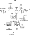
すなわち、図3において、変換部52は、RF(Radio Frequency)アンプ61、電圧電流変換回路62、負性抵抗回路63、LC共振回路64、ミキサ65、BB(Base Band)アンプ66、及び、制御部67を有する。
3, the
RFアンプ61には、アンテナ51(図2)からの変調信号が供給される。
The
RFアンプ61は、アンテナ51からの変調信号(RF信号)を増幅し、電圧電流変換回路62の入力端子INと、ミキサ65に供給する。
The
電圧電流変換回路62は、その入力端子INに供給される、RFアンプ61からの変調信号の電圧電流変換を行い、その電圧電流変換後の信号(電流)を、出力信号として、出力端子OUTから出力する。
The voltage-
なお、電圧電流変換回路62は、電圧電流変換の利得を調整することが可能になっており、その利得の調整は、制御部67によって行われる。
Note that the voltage-
負性抵抗回路63は、その端子OUTから見て、負性抵抗として機能し、負性抵抗の機能のオン/オフが可能になっている。負性抵抗回路63の端子OUTには、LC共振回路64が接続されている。
The
なお、負性抵抗回路63の負性抵抗の機能のオン/オフは、制御部67によって行われる。
Note that the negative resistance function of the
LC共振回路64には、電圧電流変換回路62が出力する出力信号が、負性抵抗回路63とLC共振回路64との接続点を経由して供給される。
An output signal output from the voltage /
また、負性抵抗回路63とLC共振回路64との接続点は、ミキサ65に接続されており、したがって、負性抵抗回路63とLC共振回路64との接続点に現れる信号(以下、接続点信号ともいう)は、ミキサ65に供給される。
Further, the connection point between the
ミキサ65は、RFアンプ61から供給される変調信号と、負性抵抗回路63とLC共振回路64との接続点からの接続点信号とをミキシング(乗算)することにより、RFアンプ61から供給される変調信号を、ベースバンド信号に変換し、BBアンプ66に供給する。
The
BBアンプ66は、ミキサ65からのベースバンド信号を増幅して出力する。
The
BBアンプ66が出力するベースバンド信号は、図示せぬLPF(Low Pass Filter)でフィルタリングされ、これにより、送信データに対応する周波数成分が抽出(取得)される。
The baseband signal output from the
なお、負性抵抗回路63の負性抵抗の機能がオンにされた場合、負性抵抗回路63とLC共振回路64とで、発振回路(発振器)が構成される。
When the negative resistance function of the
[変換部52の動作] [Operation of Conversion Unit 52]
図4は、変換部52が、注入同期検波方式で周波数変換を行う場合の動作を説明する図である。
FIG. 4 is a diagram for explaining the operation when the
注入同期検波方式で周波数変換を行う場合、制御部67は、負性抵抗回路63の負性抵抗の機能をオンにし、これにより、負性抵抗回路63とLC共振回路64とで、発振回路が構成される。
When performing the frequency conversion by the injection locking detection method, the
そして、負性抵抗回路63とLC共振回路64とで構成される発振回路には、電圧電流変換回路62が、RFアンプ61からの変調信号の電圧電流変換を行うことにより出力する出力信号が、注入信号として供給(電流注入)される。
In the oscillation circuit composed of the
負性抵抗回路63とLC共振回路64とで構成される発振回路は、電圧電流変換回路62からの出力信号を、いわば発振の種として発振する。発振回路の発振によって得られる発振信号(以下、LO(Local Oscillator)信号ともいう)は、再生キャリアとして、ミキサ65に供給される。
The oscillation circuit composed of the
ここで、LC共振回路64は、共振周波数の調整が可能であり、共振周波数を、変調信号のキャリアの周波数FCに近い周波数に調整することで、負性抵抗回路63とLC共振回路64とで構成される発振回路が発振するLO信号は、注入信号である出力信号、つまり、変調信号(のキャリア)に同期(インジェクションロック)する。
Here, the
ミキサ65は、RFアンプ61から供給される変調信号と、負性抵抗回路63とLC共振回路64とで構成される発振回路からのLO信号である再生キャリアとをミキシングすることにより、変調信号の同期検波を行い、その結果得られるベースバンド信号を、BBアンプ66に供給する。
The
なお、LC共振回路64の共振周波数の調整は、制御部67によって行われる。
The resonance frequency of the
また、負性抵抗回路63とLC共振回路64とで構成される発振回路において、LO信号を、変調信号(出力信号)に同期させるには、注入信号としての、電圧電流変換回路62が出力する出力信号のレベルの調整が必要な場合があるが、出力信号のレベルの調整は、制御部67が、電圧電流変換回路62による電圧電流変換の利得を調整することによって行われる。
In addition, in the oscillation circuit composed of the
図5は、変換部52が、自乗検波方式で周波数変換を行う場合の動作を説明する図である。
FIG. 5 is a diagram for explaining the operation when the
自乗同期検波方式で周波数変換を行う場合、制御部67は、負性抵抗回路63の負性抵抗の機能をオフにし、これにより、電圧電流変換回路62とLC共振回路64とで、LC共振回路64を負荷とする増幅器が構成される。
When performing frequency conversion by the square synchronous detection method, the
そして、電圧電流変換回路62とLC共振回路64とで構成される増幅器では、RFアンプ61からの変調信号が増幅され、変調信号を増幅した増幅信号が、ミキサ65に供給される。
In the amplifier constituted by the voltage /
ここで、説明を簡単にするために、電圧電流変換回路62とLC共振回路64とで構成される増幅器の増幅率が、例えば、1倍であるとすると、ミキサ65に供給される増幅信号は、変調信号に等しい。
Here, in order to simplify the explanation, if the amplification factor of the amplifier constituted by the voltage-
ミキサ65は、RFアンプ61から供給される変調信号と、電圧電流変換回路62とLC共振回路64とで構成される増幅器からの増幅信号である変調信号とをミキシングする(変調信号を自乗する)ことにより、変調信号の自乗検波を行い、その結果得られるベースバンド信号を、BBアンプ66に供給する。
The
なお、制御部67は、電圧電流変換回路62による電圧電流変換の利得を調整する。この利得の調整は、電圧電流変換回路62とLC共振回路64とで構成される増幅器において、変調信号が、自乗検波に適切なように増幅されるように行われる。
Note that the
[電圧電流変換回路62、負性抵抗回路63、及び、LC共振回路64の構成例]
[Configuration Example of Voltage-
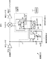
図6は、図3の電圧電流変換回路62、負性抵抗回路63、及び、LC共振回路64の構成例を示す図である。
FIG. 6 is a diagram illustrating a configuration example of the voltage-
電圧電流変換回路62は、一対のFET(Field-Effect Transistor)74及び75を用いた差動増幅器で構成されている。
The voltage-
すなわち、図6において、電圧電流変換回路62は、コンデンサ71、抵抗72及び73,FET74及び75、並びに、定電流源76を有する。
That is, in FIG. 6, the voltage-
コンデンサ71の一端は、アンプ61の出力端子に接続され、コンデンサ71の他端は、抵抗72の一端に接続されている。
One end of the capacitor 71 is connected to the output terminal of the
抵抗72の他端は、抵抗73の一端に接続され、抵抗72と73との接続点は、電源VCCに接続されている。
The other end of the
FET74のゲートは、コンデンサ71と抵抗72との接続点に接続され、FET75のゲートは、抵抗73の他端に接続されている。
The gate of the
また、FET74及び75のソースどうしは接続され、そのソースどうしの接続点は、定電流源76を介して、グランド(GND)に接続されている。
The sources of the
なお、FET74及び75のドレインは、ミキサ65に接続されている。この、ミキサ65に接続されている、FET74のドレインとFET75のドレインとの間に、再生キャリアとしてのLO信号や、増幅信号としての変調信号が現れる。
The drains of the
以上のように構成される電圧電流変換回路62においては、RFアンプ61からの変調信号が、コンデンサ71を介することにより、直流カットされ、FET74のゲートに供給される。
In the voltage-
FET74のゲートには、電源VCCによって、抵抗72を介して、バイアスがかけられており、FET75のゲートにも、電源VCCによって、抵抗73を介して、バイアスがかけられている。
The gate of the
そして、FET74のゲートには、コンデンサ71で直流カットされた変調信号が供給される。
Then, the modulation signal that is DC cut by the capacitor 71 is supplied to the gate of the
したがって、差動増幅器を構成しているFET74のドレイン・ゲート間、及び、FET75のドレイン・ゲート間には、変調信号に対応する電流、すなわち、変調信号を電圧電流変換した電流が流れる。
Therefore, a current corresponding to the modulation signal, that is, a current obtained by converting the modulation signal into a voltage-current flows between the drain and gate of the
なお、電圧電流変換回路62の電圧電流変換の利得の調整は、定電流源76に流れる電流IILを調整することにより行うことができ、電流IILの調整は、制御部67によって行われる。
Note that the adjustment of the voltage / current conversion gain of the voltage /
負性抵抗回路63は、クロスカップル接続された一対のFET81及び82で構成されている。
The
すなわち、図6において、負性抵抗回路63は、FET81及び82、並びに、定電流源83を有する。
That is, in FIG. 6, the
FET81及び82は、クロスカップル接続されている。 The FETs 81 and 82 are cross-coupled.
すなわち、FET81のゲートとFET82のドレインとが接続され、FET81のドレインとFET82のゲートとが接続されている。 That is, the gate of the FET 81 and the drain of the FET 82 are connected, and the drain of the FET 81 and the gate of the FET 82 are connected.
また、FET81及び82のソースどうしは接続され、そのソースどうしの接続点は、定電流源83を介して、グランドに接続されている。
The sources of the FETs 81 and 82 are connected to each other, and the connection point between the sources is connected to the ground via a constant
なお、FET81のドレインは、FET74のドレインとミキサ65との接続点に接続され、FET82のドレインは、FET75のドレインとミキサ65との接続点に接続されている。
The drain of the FET 81 is connected to the connection point between the drain of the
以上のように構成される負性抵抗回路63は、電流源83がオンになると、負性抵抗として機能し、電流源83がオフになると、負性抵抗の機能がオフになる。
The
LC共振回路64は、コイル91及び92、コンデンサ93及び94、並びに、抵抗95を有する。
The
コイル91及び92の一端どうしは接続され、そのコイル91と92との接続点は、電源VCCに接続されている。
One ends of the
コイル91の他端は、可変容量コンデンサであるコンデンサ93の一端に接続され、コイル92の他端は、可変容量コンデンサであるコンデンサ94の一端に接続されている。
The other end of the
コンデンサ93及び94の他端どうしは接続され、そのコンデンサ93と94との接続点は、抵抗95を介して、端子Vtuneに接続されている。
The other ends of the
そして、コイル91とコンデンサ93との接続点は、電圧電流変換回路62のFET74のドレイン(とミキサ65との接続点)、及び、負性抵抗回路63のFET81のドレイン(とミキサ65との接続点)に接続されている。
The connection point between the
同様に、コイル92とコンデンサ94との接続点は、電圧電流変換回路62のFET75のドレイン、及び、負性抵抗回路63のFET82のドレインに接続されている。
Similarly, the connection point between the
なお、コイル91及び92は、1つのコイルで構成することができる。
In addition, the
以上のように構成されるLC共振回路64については、端子Vtuneから、抵抗95を介して、コンデンサ93と94との接続点のバイアスを調整することで、LC共振回路64の共振周波数を調整することができる。コンデンサ93と94との接続点のバイアスの調整は、制御部67によって行われる。
For the
変換部52が、注入同期検波方式で、周波数変換を行う場合、制御部67は、負性抵抗回路63の電流源83をオンにすることで、負性抵抗回路63の負性抵抗の機能をオンにする。
When the
負性抵抗回路63の負性抵抗の機能がオンになることで、負性抵抗回路63とLC共振回路64との間には、電流が流れるようになり、負性抵抗回路63とLC共振回路64とで、発振回路が構成される。
When the function of the negative resistance of the
一方、電圧電流変換回路62では、RFアンプ61から供給される変調信号が、電圧電流変換され、FET74及び75のドレインには、変調信号に対応する電流が、出力信号として流れる。
On the other hand, in the voltage /
出力信号としての、変調信号に対応する電流は、FET74及び75のドレインから、負性抵抗回路63とLC共振回路64とで構成される発振回路に、注入信号として注入される。
A current corresponding to the modulation signal as an output signal is injected as an injection signal from the drains of the
発振回路は、電圧電流変換回路62からの出力信号を、発振の種として発振し、その得られるLO信号は、再生キャリアとして、ミキサ65に供給される。
The oscillation circuit oscillates the output signal from the voltage-
ここで、制御部67は、端子Vtuneから、抵抗95を介して、コンデンサ93と94との接続点のバイアスを調整することで、LC共振回路64の共振周波数を、変調信号のキャリアの周波数に近い周波数(同期の引き込み範囲)に調整する。
Here, the
LC共振回路64の共振周波数を、変調信号のキャリアの周波数に近い周波数に調整することで、負性抵抗回路63とLC共振回路64とで構成される発振回路が発振するLO信号は、注入信号である出力信号、つまり、変調信号(のキャリア)に同期(ロック)する。
By adjusting the resonance frequency of the
なお、制御部67は、コンデンサ93と94との接続点のバイアスを調整することで、LC共振回路64の共振周波数の調整を行う他、定電流源76の電流IILを調整することで、電圧電流変換回路62による電圧電流変換の利得の調整も行う。
In addition to adjusting the resonance frequency of the
すなわち、負性抵抗回路63とLC共振回路64とで構成される発振回路において、LO信号を、変調信号(出力信号)に同期させるには、LC共振回路64の共振周波数の調整と、注入信号としての、電圧電流変換回路62が出力する出力信号のレベルの調整、つまり、電圧電流変換の利得の調整とが必要であり、これらの、共振周波数の調整、及び、電圧電流変換の利得の調整は、制御部67が行う。
That is, in the oscillation circuit composed of the
一方、変換部52が、自乗同期検波方式で、周波数変換を行う場合、制御部67は、負性抵抗回路63の電流源83をオフにすることで、負性抵抗回路63の負性抵抗の機能をオフにする。
On the other hand, when the
負性抵抗回路63の負性抵抗の機能がオフになると、負性抵抗回路63には、電流が流れなくなり、電圧電流変換回路62とLC共振回路64とで、増幅器(アンプ)が構成される。
When the function of the negative resistance of the
そして、電圧電流変換回路62とLC共振回路64とで構成される増幅器では、RFアンプ61からの変調信号が増幅され、変調信号を増幅した増幅信号が、ミキサ65に供給される。
In the amplifier constituted by the voltage /
なお、制御部67は、電圧電流変換回路62とLC共振回路64とで構成される増幅器において、変調信号が、自乗検波に適切なように増幅されるように、電圧電流変換回路62による電圧電流変換の利得の調整、すなわち、定電流源の電流IILの調整を行う。
Note that the
[注入同期検波方式と自乗検波方式の特徴] [Characteristics of injection locking detection method and square detection method]
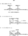
図7は、変換部52が行う周波数変換の複数の変換方式としての注入同期検波方式と自乗検波方式それぞれの特徴を説明する図である。
FIG. 7 is a diagram for explaining the characteristics of the injection locking detection method and the square detection method as a plurality of conversion methods of frequency conversion performed by the
注入同期検波方式は、自乗検波方式と比較して、相対的に、周波数変換が可能な変調信号のレベルのレンジ(受信レンジ)、及び、周波数帯域(帯域)が、広いが、自乗検波方式は、ゲインが自乗(2乗)特性を有するため、注入同期検波方式と比較して、相対的に、周波数変換が可能な変調信号のレベルのレンジ、及び、周波数帯域が、狭い。 Compared with the square detection method, the injection-locked detection method has a relatively wide modulation signal level range (reception range) and frequency band (band) compared to the square detection method, but the square detection method is Since the gain has a square (square) characteristic, the level range and frequency band of the modulation signal capable of frequency conversion are relatively narrow compared to the injection locking detection method.
また、注入同期検波方式では、低レートの変調信号については、LO信号の、変調信号への同期が不安定になるために、周波数変換を行うことが困難なことがあるが、自乗検波方式では、そのような同期の不安定を原因として、低レートの変調信号の周波数変換を行うことが困難になることは、ない。 In addition, in the injection-locked detection method, for low-rate modulation signals, it may be difficult to perform frequency conversion because the synchronization of the LO signal with the modulation signal becomes unstable. Therefore, it is not difficult to perform frequency conversion of a low-rate modulation signal due to such instability of synchronization.
したがって、低レートの変調信号の周波数変換(低レート伝送)には、注入同期検波方式より、自乗検波方式の方が適切である。 Therefore, the square detection method is more suitable than the injection locking detection method for frequency conversion (low rate transmission) of a low-rate modulation signal.
さらに、注入同期検波方式では、再生キャリアとしてのLO信号の周波数の制御(LO周波数制御)、すなわち、LC共振回路64の共振周波数の制御を行う必要があるが、自乗検波方式では、再生キャリアを生成しないので、LO周波数制御を行う必要がない。
Furthermore, in the injection locking detection method, it is necessary to control the frequency of the LO signal as a regenerated carrier (LO frequency control), that is, to control the resonance frequency of the
また、注入同期検波方式では、周波数分割された変調信号を周波数変換することにより得られるベースバンド信号から、データ系列(送信データ)の選択(分離)を行うこと(BB(Baseband)帯で信号選択)が可能であるが、自乗検波方式では、そのようなデータ系列の選択を行うことが困難である。 In addition, the injection-locked detection method selects (separates) the data series (transmission data) from the baseband signal obtained by frequency-converting the frequency-divided modulated signal (signal selection in the BB (Baseband) band) However, in the square detection method, it is difficult to select such a data series.
ここで、図8は、ベースバンド信号からの、データ系列の選択を説明する図である。 Here, FIG. 8 is a diagram for explaining selection of a data series from a baseband signal.
図8Aは、周波数分割された変調信号#1及び#2のスペクトラムを示す図である。 FIG. 8A is a diagram showing the spectrum of the frequency-divided modulated signals # 1 and # 2.
図8Aにおいて、変調信号#1は、ある周波数f1のキャリアを、あるデータレートのデータ系列#1で変調した信号であり、変調信号#2は、周波数f1よりも高い周波数f2のキャリアを、あるデータレートのデータ系列#2で変調した信号である。 In FIG. 8A, a modulation signal # 1 is a signal obtained by modulating a carrier of a certain frequency f1 with a data sequence # 1 of a certain data rate, and the modulation signal # 2 is a carrier of a frequency f2 higher than the frequency f1. It is a signal modulated by data sequence # 2 at the data rate.
キャリアの周波数f1及びf2として、変調信号#1及び#2の周波数帯域が重ならない周波数を用いることにより、変調信号#1及び#2を、同時に送信することができる。 Modulation signals # 1 and # 2 can be transmitted simultaneously by using frequencies at which the frequency bands of modulation signals # 1 and # 2 do not overlap as carrier frequencies f1 and f2.
すなわち、例えば、半導体チップ31ないし34において、任意の2つの半導体チップのうちの一方の半導体チップから、変調信号#1を、他方の半導体チップに送信し、他方の半導体チップから、変調信号#2を、一方の半導体チップに送信することを、同時に行うことができる。 That is, for example, in the semiconductor chips 31 to 34, the modulation signal # 1 is transmitted from one of the two arbitrary semiconductor chips to the other semiconductor chip, and the modulation signal # 2 is transmitted from the other semiconductor chip. Can be simultaneously transmitted to one semiconductor chip.
また、例えば、半導体チップ31ないし34において、任意の3つの半導体チップである第1チップ、第2チップ、及び、第3チップのうちの、第1チップから、変調信号#1を、第2チップに送信し、変調信号#2を、第3チップに送信することを、同時に行うことができる。 Further, for example, in the semiconductor chips 31 to 34, the modulation signal # 1 is transmitted from the first chip among the first chip, the second chip, and the third chip, which are arbitrary three semiconductor chips, to the second chip. And transmitting the modulation signal # 2 to the third chip can be performed simultaneously.
図8Bは、注入同期検波方式で、変調信号#1及び#2の周波数変換を行って得られるベースバンド信号のスペクトラムを示す図である。 FIG. 8B is a diagram showing a spectrum of a baseband signal obtained by performing frequency conversion of modulated signals # 1 and # 2 by the injection locking detection method.
注入同期検波方式において、例えば、再生キャリアとしてのLO信号を、変調信号#1に同期させたとすると、データ系列#1の周波数成分は、DC(Direct Current)付近に広がり、データ系列#2の周波数成分は、周波数f2-f1を中心に広がる。 In the injection locking detection method, for example, if the LO signal as a reproduction carrier is synchronized with the modulation signal # 1, the frequency component of the data sequence # 1 spreads near the DC (Direct Current), and the frequency of the data sequence # 2 The component spreads around the frequency f2-f1.
したがって、データ系列#1は、ベースバンド信号を、LPFでフィルタリングすることにより抽出することができる。 Therefore, the data sequence # 1 can be extracted by filtering the baseband signal with the LPF.
また、注入同期検波方式では、再生キャリアとしてのLO信号を、変調信号#2に同期させることで、データ系列#2の周波数成分が、DC付近に広がるので、やはり、ベースバンド信号を、LPFでフィルタリングすることにより、データ系列#2を抽出することができる。 In addition, in the injection locking detection method, the LO signal as the reproduction carrier is synchronized with the modulation signal # 2, so that the frequency component of the data sequence # 2 spreads around DC. Data series # 2 can be extracted by filtering.
以上のように、注入同期検波方式によれば、周波数分割された変調信号#1及び#2を周波数変換することにより得られるベースバンド信号から、データ系列#1又は#2を選択(分離)することができる。 As described above, according to the injection locking detection method, the data sequence # 1 or # 2 is selected (separated) from the baseband signal obtained by frequency-converting the frequency-divided modulated signals # 1 and # 2. be able to.
図8Cは、自乗検波方式で、変調信号#1及び#2の周波数変換を行って得られるベースバンド信号のスペクトラムを示す図である。 FIG. 8C is a diagram illustrating a spectrum of a baseband signal obtained by performing frequency conversion of modulated signals # 1 and # 2 using the square detection method.
自乗検波方式では、変調信号#1及び#2(の全体)が自乗されるため、その結果得られるベースバンド信号においては、データ系列#1及び#2の周波数成分の両方が、DC付近に広がるとともに、周波数f2-f1を中心に広がる。 In the square detection method, since the modulation signals # 1 and # 2 (the whole) are squared, both frequency components of the data series # 1 and # 2 spread in the vicinity of DC in the resulting baseband signal. At the same time, it spreads around the frequency f2-f1.
したがって、自乗検波方式で得られるベースバンド信号では、データ系列#1及び#2の周波数成分が重畳されてしまうため、自乗検波方式によれば、周波数分割された変調信号#1及び#2を周波数変換することにより得られるベースバンド信号から、データ系列#1や#2を選択することが困難となる。 Therefore, in the baseband signal obtained by the square detection method, the frequency components of the data series # 1 and # 2 are superimposed. Therefore, according to the square detection method, the frequency-divided modulation signals # 1 and # 2 are frequency-converted. It becomes difficult to select the data series # 1 and # 2 from the baseband signal obtained by the conversion.
以上のように、注入同期検波方式では、周波数分割された変調信号を周波数変換することにより得られるベースバンド信号から、データ系列の選択を行うことが可能であるが、自乗検波方式では、そのようなデータ系列の選択を行うことが困難である。 As described above, in the injection locking detection method, it is possible to select a data series from a baseband signal obtained by frequency-converting a frequency-divided modulation signal. In the square detection method, however, It is difficult to select a correct data series.
[変換方式の選択] [Select conversion method]
図9は、変換方式の選択を説明する図である。 FIG. 9 is a diagram illustrating selection of a conversion method.
注入同期検波方式と自乗検波方式とのそれぞれは、図7及び図8で説明したような特徴を有するので、変換部52では、その特徴を考慮して、周波数変換の変換方式を選択することができる。
Each of the injection locking detection method and the square detection method has the characteristics as described with reference to FIGS. 7 and 8, so that the
変換部52において、変換方式の選択は、制御部67によって行われる。
In the
図9は、変調信号のデータレートに応じた、変換方式の選択を説明する図である。 FIG. 9 is a diagram illustrating the selection of the conversion method according to the data rate of the modulation signal.
制御部67では、例えば、変調信号のデータレートに応じ、画像のデータ等の高レートの変調信号が送信されてくる場合には、注入同期検波方式を選択し、制御データ等の低レートの変調信号が送信されてくる場合には、自乗検波方式を選択することができる。
For example, when a high-rate modulation signal such as image data is transmitted according to the data rate of the modulation signal, the
変調信号として、高レート、又は、低レートの変調信号のいずれが送信されてくるかの情報は、例えば、制御部67において、変調信号を送信してくる送信装置40(図2)から、図示せぬ有線による配線を介して受信することができる。
For example, information on whether a high-rate modulation signal or a low-rate modulation signal is transmitted as the modulation signal is transmitted from the transmission device 40 (FIG. 2) that transmits the modulation signal in the
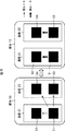
図9では、あるタイミングにおいて、半導体チップ31から、半導体チップ32ないし34のそれぞれに、低レートの変調信号である、例えば、制御データの変調信号が送信されている。
In FIG. 9, at a certain timing, a modulation signal of, for example, control data, which is a low-rate modulation signal, is transmitted from the
さらに、図9では、他のタイミングにおいて、半導体チップ31から、半導体チップ32に対して、高レートの変調信号である、例えば、画像のデータの変調信号が送信されているとともに、半導体チップ33から、半導体チップ34に対しても、高レートの変調信号が送信されている。
Further, in FIG. 9, at another timing, the
半導体チップ31から、半導体チップ32ないし34のそれぞれに、低レートの変調信号が送信される場合、その低レートの変調信号を受信する半導体チップ32ないし34それぞれの制御部67では、自乗検波方式が選択される。
When a low-rate modulation signal is transmitted from the
また、半導体チップ31から、半導体チップ32に対して、高レートの変調信号が送信されるとともに、半導体チップ33から、半導体チップ34に対して、高レートの変調信号が送信される場合、高レートの変調信号を受信する半導体チップ32及び34それぞれの制御部67では、注入同期検波方式が選択される。
Further, when a high-rate modulation signal is transmitted from the
図10は、変調信号を送信する送信装置40(図2)からの指示に応じた、変換方式の選択を説明する図である。 FIG. 10 is a diagram for explaining the selection of the conversion method according to the instruction from the transmission device 40 (FIG. 2) that transmits the modulated signal.
制御部67では、例えば、デフォルトで、自乗検波方式を選択することができる。さらに、制御部67では、変調信号を送信してくる送信装置40からの指示に応じ、例えば、デフォルトの変換方式でない注入同期検波方式が指示された場合には、注入同期検波方式を選択することができる。
In the
図10では、半導体チップ31から、半導体チップ32ないし34のそれぞれに、所定の周波数のキャリアの低レートの変調信号として、制御データの変調信号が送信されている。
In FIG. 10, a modulation signal of control data is transmitted from the
半導体チップ32ないし34それぞれの制御部67では、半導体チップ31から、注入同期検波方式の指示がない場合には、デフォルトで、自乗検波方式を選択する。したがって、半導体チップ32ないし34それぞれの受信装置50(図2)では、半導体チップ31からの変調信号の周波数変換が、自乗検波方式で行われる。
When there is no instruction for the injection locking detection method from the
その後、例えば、画像のデータ等の高レートのデータの変調信号を、半導体チップ31から半導体チップ32に送信するとともに、半導体チップ33から半導体チップ34に送信するために、半導体チップ31が、半導体チップ32及び34への注入同期検波方式の指示、並びに、半導体チップ33への高レートのデータの送信の指示を含む制御データの変調信号を送信すると、半導体チップ32及び34それぞれの制御部67では、半導体チップ31からの制御データ(の変調信号)に含まれる、注入同期検波方式の指示に従い、注入同期検波方式を選択する。
After that, for example, in order to transmit a modulation signal of high-rate data such as image data from the
さらに、半導体チップ31は、高レートのデータの変調信号の送信を開始する。また、半導体チップ33は、半導体チップ31からの制御データに含まれる指示に従い、高レートのデータの変調信号の送信を開始する。
Further, the
そして、半導体チップ32の受信装置50では、半導体チップ31からの高レートのデータの変調信号の周波数変換が、注入同期検波方式で行われる。半導体チップ34の受信装置50でも、半導体チップ33からの高レートのデータの変調信号の周波数変換が、注入同期検波方式で行われる。
In the receiving device 50 of the
その後、半導体チップ32の制御部67は、半導体チップ31からの高レートのデータ(の変調信号)の受信が完了すると、自乗検波方式を選択する。
Thereafter, the
半導体チップ34の制御部67も、半導体チップ33からの高レートのデータの受信が完了すると、自乗検波方式を選択する。
The
なお、半導体チップ31による、高レート(のデータ)の変調信号の送信と、半導体チップ33による、高レートの変調信号の送信とが、時間的に重複して行われることがない場合には、半導体チップ31が送信する高レートの変調信号のキャリアの周波数f2と、半導体チップ33が送信する高レートの変調信号のキャリアの周波数f3としては、半導体チップ31及び33のそれぞれが送信する変調信号の周波数帯域どうしが重なるような周波数であっても使用することができる。
When the transmission of the high-rate (data) modulation signal by the
但し、半導体チップ31による、高レートの変調信号の送信と、半導体チップ33による、高レートの変調信号の送信とが、時間的に重複して行われることがある場合には、周波数f2とf3としては、半導体チップ31及び33のそれぞれが送信する変調信号の周波数帯域どうしが重ならないような周波数を使用する必要がある。
However, when the transmission of the high-rate modulation signal by the
半導体チップ31による、高レートの変調信号の送信と、半導体チップ33による、高レートの変調信号の送信とが、時間的に重複して行われる場合、注入同期検波方式を選択している半導体チップ32の変換部52では、同時に送信されてくる、周波数f2のキャリアの変調信号、及び、周波数f3のキャリアの変調信号のうちの、周波数f2のキャリアの変調信号、つまり、半導体チップ31からの変調信号に同期したLO信号を生成(発振)し、そのLO信号を再生キャリアとして用いて、周波数変換を行う。
When the transmission of the high-rate modulation signal by the
そして、半導体チップ32の変換部52は、周波数変換によって得られるベースバンド信号からの、図8で説明したデータ系列の選択を行う。
Then, the
同様に、半導体チップ34の変換部52では、同時に送信されてくる、周波数f2のキャリアの変調信号、及び、周波数f3のキャリアの変調信号のうちの、周波数f3のキャリアの変調信号、つまり、半導体チップ33からの変調信号に同期したLO信号を生成し、そのLO信号を再生キャリアとして用いて、周波数変換を行う。
Similarly, in the
そして、半導体チップ34の変換部52は、周波数変換によって得られるベースバンド信号からの、図8で説明したデータ系列の選択を行う。
Then, the
周波数変換の変換方式の選択は、以上のように、変調信号のデータレートや、変調信号を送信する送信装置40からの指示に応じて行う他、その他の方法によって行うこともできる。 As described above, the conversion method for frequency conversion can be selected according to the data rate of the modulated signal or an instruction from the transmitting apparatus 40 that transmits the modulated signal, or by other methods.
すなわち、制御部67では、例えば、変調信号の受信レベルに応じ、変調信号の(レベルの)受信レベルが低い場合には、受信レンジが相対的に広い注入同期検波方式を選択し、変調信号の受信レベルが高い場合には、受信レンジが相対的に狭い自乗検波方式を選択することができる。
That is, in the
なお、注入同期検波方式は、受信レンジが相対的に広いので、制御部67は、変調信号の受信レベルについては、その受信レベルの高低に関係なく、常時、注入同期検波方式を選択することができる。
Since the injection locking detection method has a relatively wide reception range, the
但し、自乗検波方式は、負性抵抗回路63が負性抵抗として機能する注入同期検波方式に比較して、消費電力が低いので、変調信号の受信レベルが高い場合に、自乗検波方式を選択することで、常時、注入同期検波方式を選択する場合に比較して、消費電力を抑制することができる。
However, since the square detection method consumes less power than the injection locking detection method in which the
また、通信を行う2つの半導体チップどうしを、十分に近い距離ではあるが、比較的離れた距離に配置せざるを得ないことがある。 In addition, two semiconductor chips that communicate with each other may be forced to be arranged at a relatively close distance although they are sufficiently close to each other.
すなわち、例えば、3つの半導体チップである第1チップないし第3チップにおいて、第1チップが、第2チップから送信されてくる変調信号を受信する場合と、第3チップから送信されてくる変調信号を受信する場合とがあり、さらに、第1チップと第2チップとは、比較的近い距離D1に配置することができるが、第1チップと第3チップとは、距離D1よりも離れた距離D2にしか配置することができないことがある。 That is, for example, in the first to third chips, which are three semiconductor chips, the first chip receives the modulation signal transmitted from the second chip, and the modulation signal transmitted from the third chip. In addition, the first chip and the second chip can be disposed at a relatively close distance D1, but the first chip and the third chip are separated from each other by a distance D1. Sometimes it can only be placed in D2.
この場合、第2チップ及び第3チップからの変調信号を受信する第1チップの制御部67は、変調信号を送信してくる通信相手が、第2チップ及び第3チップのうちのいずれであるかによって、変換方式を選択することができる。
In this case, the
すなわち、第1チップの制御部67では、第1チップと比較的近い距離D1に配置された第2チップが通信相手である場合には、そのような近い距離D1に配置された第2チップから送信されてくる変調信号の受信レベルが高いことを考慮して、受信レンジが相対的に狭い自乗検波方式を選択することができる。
That is, in the
また、第1チップの制御部67では、第1チップから距離D1より離れた距離D2に配置された第3チップが通信相手である場合には、そのような離れた距離D2に配置された第3チップから送信されてくる変調信号の受信レベルが低いことを考慮して、受信レンジが相対的に広い注入同期検波方式を選択することができる。
Further, in the
さらに、例えば、上述のように、第1チップが、第2チップから送信されてくる変調信号を受信することと、第3チップから送信されてくる変調信号を受信することとがある場合において、第2チップが、1つのキャリアを変調した変調信号を送信し、第3チップが、複数のキャリアを変調した複数の変調信号を周波数分割で送信するときにも、第1チップの制御部67は、変調信号を送信してくる通信相手が、第2チップ及び第3チップのうちのいずれであるかによって、変換方式を選択することができる。
Further, for example, as described above, when the first chip receives a modulated signal transmitted from the second chip and receives a modulated signal transmitted from the third chip, Even when the second chip transmits a modulated signal obtained by modulating one carrier and the third chip transmits a plurality of modulated signals obtained by modulating a plurality of carriers by frequency division, the
すなわち、第1チップの制御部67では、1つのキャリアを変調した変調信号を送信してくる第2チップが通信相手である場合には、図8で説明したデータ系列の選択の必要がないので、データ系列の選択が困難ではあるが、消費電力が低い自乗検波方式を選択することができる。
That is, in the
また、第1チップの制御部67では、複数の変調信号を周波数分割で送信してくる第3チップが通信相手である場合には、図8で説明したデータ系列の選択が必要なので、データ系列の選択が可能な注入同期検波方式を選択することができる。
Further, in the
さらに、制御部67では、変換部52の同期の状態に応じ、デフォルトでは、例えば、注入同期検波方式を選択し、注入同期検波方式において、再生キャリアとしてのLO信号を、変調信号に同期させることができない場合に、自乗検波方式を選択することができる。
Further, the
また、制御部67では、変換方式を指示するメカニカルな、又は、GUI(Graphical User Interface)等の操作部(図示せず)の操作に応じて、変換方式を選択することができる。
Further, the
<第2実施の形態> <Second Embodiment>
[電子機器の第2実施の形態の構成例] [Configuration Example of Second Embodiment of Electronic Device]
図11は、本発明を適用した電子機器の第2実施の形態の構成例を示す平面図である。 FIG. 11 is a plan view showing a configuration example of a second embodiment of an electronic apparatus to which the present invention is applied.
なお、図中、図1の場合と対応する部分については、同一の符号を付してあり、以下では、その説明は、適宜省略する。 In the figure, portions corresponding to those in FIG. 1 are denoted by the same reference numerals, and description thereof will be omitted as appropriate.
図11の電子機器では、半導体チップ31及び32が配置された基板21、並びに、半導体チップ33及び34が配置された基板22が、筐体内10に収容されており、したがって、図11の電子機器は、図1の電子機器と同様に構成されている。 In the electronic device of FIG. 11, the substrate 21 on which the semiconductor chips 31 and 32 are arranged and the substrate 22 on which the semiconductor chips 33 and 34 are arranged are accommodated in the housing 10, and accordingly, the electronic device of FIG. Is configured in the same manner as the electronic apparatus of FIG.
但し、図11の電子機器では、半導体チップ31ないし34それぞれの変換部52において、周波数変換を行う変換方式が、1つだけに固定されている。
However, in the electronic apparatus shown in FIG. 11, the conversion method for performing frequency conversion is fixed to only one in the
すなわち、図1の電子機器では、半導体チップ31ないし34それぞれの変換部52において、複数の変換方式のいずれかで、周波数変換を行うことが可能であり、その複数の変換方式の中から、周波数変換を行う1つの変換方式を、いわば動的に選択することができる。
That is, in the electronic device of FIG. 1, the
一方、図11の電子機器では、半導体チップ31ないし34それぞれの変換部52において、複数の変換方式のいずれかで、周波数変換を行うことが可能であり、その点は、図1の電子機器と共通するが、複数の変換方式の中からあらかじめ選択された1つの変換方式でのみ、周波数変換を行い、変換方式が、複数の変換方式の中からあらかじめ選択された1つの変換方式に固定されている点で、図1の電子機器と相違する。
On the other hand, in the electronic device of FIG. 11, the
図11の電子機器では、半導体チップ31ないし34のそれぞれについて、受信する変調信号に応じて、周波数変換の変換方式が固定(あらかじめ選択)されている。 In the electronic device of FIG. 11, the conversion method of frequency conversion is fixed (pre-selected) for each of the semiconductor chips 31 to 34 in accordance with the received modulation signal.
すなわち、図11の電子機器では、半導体チップ31は、半導体チップ32に、高レートの変調信号を送信することと、半導体チップ33に、低レートの変調信号を送信することがある。
That is, in the electronic device of FIG. 11, the
半導体チップ32は、半導体チップ34に、高レートの変調信号を送信することがある。
The
半導体チップ33は、半導体チップ31に、低レートの変調信号を送信することと、半導体チップ34に、高レートの変調信号を送信することがある。
The
半導体チップ34は、半導体チップ31に、低レートの変調信号を送信することがある。
The
したがって、図11の電子機器では、半導体チップ31は、半導体チップ33からの低レートの変調信号と、半導体チップ34からの低レートの変調信号とを受信することはあるが、高レートの変調信号を受信することはない。
Therefore, in the electronic device of FIG. 11, the
また、半導体チップ32は、半導体チップ31からの高レートの変調信号を受信することはあるが、低レートの変調信号を受信することはない。
In addition, the
さらに、半導体チップ33は、半導体チップ31からの低レートの変調信号を受信することはあるが、高レートの変調信号を受信することはない。
Further, the
また、半導体チップ34は、半導体チップ32からの高レートの変調信号と、半導体チップ33からの高レートの変調信号とを受信することはあるが、低レートの変調信号を受信することはない。
Further, the
そこで、図11では、低レートの変調信号を受信することはあるが、高レートの変調信号を受信することがない半導体チップ31及び33それぞれの変換部52については、周波数変換の変換方式が、低レートの変調信号の周波数変換に適した、例えば、自乗検波方式に固定されている。
Therefore, in FIG. 11, the conversion method of the frequency conversion is used for each of the
また、高レートの変調信号を受信することはあるが、低レートの変調信号を受信することがない半導体チップ32及び34それぞれの変換部52については、周波数変換の変換方式が、高レートの変調信号の周波数変換に適した、例えば、注入同期検波方式に固定されている。
In addition, for the
以上のように、図11の電子機器では、半導体チップ31ないし34それぞれの変換部52において、周波数変換の変換方式が、受信する変調信号に応じて異なっている。
As described above, in the electronic device of FIG. 11, the conversion method of frequency conversion in the
なお、変換方式を、複数の変換方式の中からあらかじめ選択された1つの変換方式に固定する場合、変換部52は、図3ないし図6等に示したように、複数の変換方式の中から、周波数変換を行う1つの変換方式を動的に選択することが可能なように構成することができる。
When the conversion method is fixed to one conversion method selected in advance from a plurality of conversion methods, the
但し、図11の電子機器では、変換方式が、複数の変換方式の中からあらかじめ選択された1つの変換方式に固定されるので、変換部52は、その固定の変換方式のみで、周波数変換を行うように構成することができる。
However, in the electronic device of FIG. 11, the conversion method is fixed to one conversion method selected in advance from a plurality of conversion methods, so that the
すなわち、図11の電子機器については、半導体チップ31及び33それぞれの変換部52は、変換方式が自乗検波方式に固定されるので、自乗検波方式のみで、周波数変換を行うように構成することができる。同様に、半導体チップ32及び34それぞれの変換部52は、変換方式が注入同期検波方式に固定されるので、注入同期検波方式のみで、周波数変換を行うように構成することができる。
That is, in the electronic device of FIG. 11, the
図12は、自乗検波方式のみで、周波数変換を行う変換部52の構成例を示す図である。
FIG. 12 is a diagram illustrating a configuration example of the
図中、図3の場合と対応する部分については、同一の符号を付してあり、以下では、その説明は、適宜省略する。 In the figure, portions corresponding to those in FIG. 3 are denoted by the same reference numerals, and description thereof will be omitted as appropriate.
図12の変換部52は、RFアンプ61、ミキサ65、及び、BBアンプ66を有する点で、図3の場合と共通する。
12 is common to the case of FIG. 3 in that it includes an
但し、図12の変換部52は、電圧電流変換回路62、負性抵抗回路63、LC共振回路64、及び、制御部67が設けられておらず、増幅器101が新たに設けられている点で、図3の場合と相違する。
However, the
図12の変換部52では、増幅器101に、RFアンプ61から変調信号が供給される。
In the
増幅器101は、図5で説明した、電圧電流変換回路62とLC共振回路64とで構成される増幅器と同様の機能を有しており、RFアンプ61からの変調信号を増幅し、その結果得られる増幅信号を、ミキサ65に供給する。
The
ミキサ65は、RFアンプ61から供給される変調信号と、増幅器101からの増幅信号とをミキシングする(変調信号を自乗する)ことにより、変調信号の自乗検波を行い、その結果得られるベースバンド信号を、BBアンプ66に供給する。
The
図13は、注入同期検波方式のみで、周波数変換を行う変換部52の構成例を示す図である。
FIG. 13 is a diagram illustrating a configuration example of the
図中、図3の場合と対応する部分については、同一の符号を付してあり、以下では、その説明は、適宜省略する。 In the figure, portions corresponding to those in FIG. 3 are denoted by the same reference numerals, and description thereof will be omitted as appropriate.
図13の変換部52は、RFアンプ61、ミキサ65、及び、BBアンプ66を有する点で、図3の場合と共通する。
The
但し、図12の変換部52は、電圧電流変換回路62、負性抵抗回路63、LC共振回路64、及び、制御部67が設けられておらず、発振回路111が新たに設けられている点で、図3の場合と相違する。
However, the
図13の変換部52では、発振回路111に、RFアンプ61から変調信号が、注入信号として供給される。
In the
発振回路111は、図4で説明した、負性抵抗回路63とLC共振回路64とで構成される発振回路と同様の機能を有しており、RFアンプ61からの注入信号としての変調信号に同期したLO信号を生成(発振)し、再生キャリアとして、ミキサ65に供給する。
The
ミキサ65は、RFアンプ61から供給される変調信号と、発振回路111からの再生キャリアとをミキシングすることにより、変調信号の注入同期検波を行い、その結果得られるベースバンド信号を、BBアンプ66に供給する。
The
なお、本発明の実施の形態は、上述した実施の形態に限定されるものではなく、本発明の要旨を逸脱しない範囲において種々の変更が可能である。 The embodiment of the present invention is not limited to the above-described embodiment, and various modifications can be made without departing from the gist of the present invention.
すなわち、例えば、図11の電子機器において、半導体チップ31ないし34の一部については、複数の変換方式の中からあらかじめ選択された1つの変換方式のみで、周波数変換を行うように、変換部52を構成し、残りについては、複数の変換方式の中から、周波数変換を行う1つの変換方式を動的に選択することが可能なように、変換部52を構成することができる。
That is, for example, in the electronic device of FIG. 11, the
10 筐体, 21,22 基板, 31ないし34 半導体チップ, 40 送信装置, 41 発振器, 42 ミキサ, 43 アンプ, 44 アンテナ, 50 受信装置, 51 アンテナ, 52 変換部, 61 RFアンプ, 62 電圧電流変換回路, 63 負性抵抗回路, 64 LC共振回路, 65 ミキサ, 66 BBアンプ, 67 制御部, 71 コンデンサ, 72,73 抵抗, 74,75 FET, 76 定電流源, 81,82 FET, 83 定電流源, 91,92 コイル, 93,94 コンデンサ, 95 抵抗, 101 増幅器, 111 発振回路 10 housings, 21 and 22 substrates, 31 to 34 semiconductor chips, 40 transmitters, 41 oscillators, 42 mixers, 43 amplifiers, 44 antennas, 50 receivers, 51 antennas, 52 converters, 61 RF amplifiers, 62 voltage-current converters Circuit, 63 negative resistance circuit, 64 LC resonance circuit, 65 mixer, 66 BB amplifier, 67 control unit, 71 capacitor, 72, 73 resistance, 74, 75 FET, 76 constant current source, 81, 82 FET, 83 constant current Source, 91, 92 coil, 93, 94 capacitor, 95 resistor, 101 amplifier, 111 oscillator circuit
Claims (18)
前記変換部は、複数の変換方式で、前記周波数変換を行うことが可能であり、前記複数の変換方式の中から選択された1つの変換方式で、前記変調信号の周波数変換を行う
受信装置。 A conversion unit that performs frequency conversion of a modulated signal transmitted wirelessly,
The receiving unit is capable of performing the frequency conversion using a plurality of conversion methods, and performing the frequency conversion of the modulated signal using one conversion method selected from the plurality of conversion methods.
前記変換部は、前記注入同期検波方式、又は、前記自乗検波方式で、前記変調信号を、ベースバンドの信号に変換する
請求項1に記載の受信装置。 The plurality of conversion methods are an injection locking detection method and a square detection method,
The receiving device according to claim 1, wherein the conversion unit converts the modulation signal into a baseband signal by the injection locking detection method or the square detection method.
前記変調信号の電圧電流変換を行う電圧電流変換回路と、
前記電圧電流変換回路が、前記変調信号の電圧電流変換を行うことにより出力する出力信号が供給される共振回路と、
前記共振回路に接続され、負性抵抗の機能のオン/オフが可能な負性抵抗回路と、
前記変調信号と、前記共振回路が出力する信号とをミキシングするミキサと
を有する
請求項2に記載の受信装置。 The converter is
A voltage-current conversion circuit for performing voltage-current conversion of the modulation signal;
A resonance circuit to which an output signal output by the voltage-current conversion circuit performing voltage-current conversion of the modulation signal is supplied;
A negative resistance circuit connected to the resonant circuit and capable of turning on / off the function of the negative resistance;
The receiving apparatus according to claim 2, further comprising: a mixer that mixes the modulation signal and a signal output from the resonance circuit.
前記負性抵抗回路の負性抵抗の機能がオンにされることにより、前記共振回路と前記負性抵抗回路とで、発振回路が構成され、
前記電圧電流変換回路が出力する前記出力信号が、前記発振回路に供給されることにより、前記発振回路は、前記変調信号と同期した再生キャリアを出力し、
前記ミキサは、前記変調信号と、前記再生キャリアとをミキシングし、
前記変換部が、前記自乗検波方式で、前記周波数変換を行う場合、
前記負性抵抗回路の負性抵抗の機能がオフにされ、
前記電圧電流変換回路と前記共振回路とで、増幅器が構成され、
前記増幅器は、前記変調信号を増幅して、増幅信号を出力し、
前記ミキサは、前記変調信号と、前記増幅信号とをミキシングする
請求項3に記載の受信装置。 When the conversion unit performs the frequency conversion by the injection locking detection method,
By turning on the function of the negative resistance of the negative resistance circuit, the resonance circuit and the negative resistance circuit constitute an oscillation circuit,
The output signal output from the voltage-current conversion circuit is supplied to the oscillation circuit, so that the oscillation circuit outputs a reproduction carrier synchronized with the modulation signal,
The mixer mixes the modulated signal and the reproduction carrier,
When the conversion unit performs the frequency conversion by the square detection method,
The function of the negative resistance of the negative resistance circuit is turned off,
The voltage-current conversion circuit and the resonance circuit constitute an amplifier,
The amplifier amplifies the modulated signal and outputs an amplified signal;
The receiving device according to claim 3, wherein the mixer mixes the modulated signal and the amplified signal.
請求項3に記載の受信装置。 The receiving device according to claim 3, wherein the voltage-current conversion circuit is capable of adjusting a gain of the voltage-current conversion.
請求項3に記載の受信装置。 The receiving device according to claim 3, wherein the resonance circuit is capable of adjusting a resonance frequency.
前記負性抵抗回路は、クロスカップル接続された一対のトランジスタで構成される
請求項3に記載の受信装置。 The voltage-current conversion circuit is composed of a differential amplifier using a pair of transistors,
The receiving device according to claim 3, wherein the negative resistance circuit includes a pair of transistors that are cross-coupled.
請求項1に記載の受信装置。 The receiving device according to claim 1, wherein the conversion unit selects the conversion method in accordance with an operation of an operation unit that instructs the conversion method.
請求項1に記載の受信装置。 The receiving device according to claim 1, wherein the conversion unit selects the conversion method according to a data rate of the modulated signal.
請求項1に記載の受信装置。 The receiving device according to claim 1, wherein the conversion unit selects the conversion method according to a level of the modulation signal.
請求項1に記載の受信装置。 The receiving device according to claim 1, wherein the conversion unit selects the conversion method in accordance with an instruction from a transmitting device that transmits the modulated signal.
請求項1に記載の受信装置。 The receiving device according to claim 1, wherein the receiving device is installed in a casing of an electronic device together with the transmitting device that transmits the modulated signal.
請求項1に記載の受信装置。 The receiving apparatus according to claim 1, wherein the modulation signal is a millimeter-wave band signal.
請求項1に記載の受信装置。 The receiving device according to claim 1, wherein the conversion unit is formed on a one-chip semiconductor chip.
の前記変換部が、複数の変換方式で、前記周波数変換を行うことが可能であり、前記複数の変換方式の中から選択された1つの変換方式で、前記変調信号の周波数変換を行う
受信方法。 The conversion unit of the reception device including a conversion unit that performs frequency conversion of a modulation signal transmitted wirelessly can perform the frequency conversion by a plurality of conversion methods, A receiving method for performing frequency conversion of the modulated signal by one selected conversion method.
前記変調信号を受信する受信装置が形成された複数の半導体チップと
が、筐体内に収容され、
前記受信装置は、前記変調信号の周波数変換を行う変換部を有し、
前記複数の半導体チップのうちの、1の半導体チップの受信装置の前記変換部と、他の1の半導体チップの受信装置の前記変換部とは、前記周波数変換を行う複数の変換方式のうちの異なる変換方式で、前記変調信号の周波数変換を行う
電子機器。 One or more semiconductor chips formed with a transmitter that wirelessly transmits a modulated signal obtained by modulating a carrier;
A plurality of semiconductor chips formed with a receiving device for receiving the modulated signal, and housed in a housing;
The receiving apparatus includes a conversion unit that performs frequency conversion of the modulated signal,
Among the plurality of semiconductor chips, the conversion unit of the reception device of one semiconductor chip and the conversion unit of the reception device of the other semiconductor chip are among the conversion methods for performing the frequency conversion. An electronic device that performs frequency conversion of the modulated signal using different conversion methods.
前記1の半導体チップの受信装置の前記変換部は、前記注入同期検波方式で、前記変調信号を、ベースバンドの信号に変換し、
前記他の1の半導体チップの受信装置の前記変換部は、前記自乗検波方式で、前記変調信号を、ベースバンドの信号に変換する
請求項16に記載の電子機器。 The plurality of conversion methods are an injection locking detection method and a square detection method,
The converter of the semiconductor chip receiver of the first aspect converts the modulation signal into a baseband signal by the injection locking detection method,
The electronic device according to claim 16, wherein the conversion unit of the other one semiconductor chip receiving device converts the modulation signal into a baseband signal by the square detection method.
請求項16に記載の電子機器。 The electronic apparatus according to claim 16, wherein the modulation signal is a millimeter-wave band signal.
Priority Applications (3)
| Application Number | Priority Date | Filing Date | Title |
|---|---|---|---|
| JP2010255569A JP5630648B2 (en) | 2010-11-16 | 2010-11-16 | Reception device, reception method, and electronic device |
| US13/200,931 US8498583B2 (en) | 2010-11-16 | 2011-10-05 | Signal receiving apparatus, signal receiving method and electronic apparatus |
| CN2011103530487A CN102469051A (en) | 2010-11-16 | 2011-11-09 | Signal receiving apparatus, signal receiving method and electronic apparatus |
Applications Claiming Priority (1)
| Application Number | Priority Date | Filing Date | Title |
|---|---|---|---|
| JP2010255569A JP5630648B2 (en) | 2010-11-16 | 2010-11-16 | Reception device, reception method, and electronic device |
Publications (2)
| Publication Number | Publication Date |
|---|---|
| JP2012109700A true JP2012109700A (en) | 2012-06-07 |
| JP5630648B2 JP5630648B2 (en) | 2014-11-26 |
Family
ID=46048197
Family Applications (1)
| Application Number | Title | Priority Date | Filing Date |
|---|---|---|---|
| JP2010255569A Expired - Fee Related JP5630648B2 (en) | 2010-11-16 | 2010-11-16 | Reception device, reception method, and electronic device |
Country Status (3)
| Country | Link |
|---|---|
| US (1) | US8498583B2 (en) |
| JP (1) | JP5630648B2 (en) |
| CN (1) | CN102469051A (en) |
Cited By (2)
| Publication number | Priority date | Publication date | Assignee | Title |
|---|---|---|---|---|
| WO2017122555A1 (en) | 2016-01-15 | 2017-07-20 | ソニー株式会社 | Transmitter, transmission method, receiver, and receiving method |
| WO2017183478A1 (en) * | 2016-04-22 | 2017-10-26 | ソニー株式会社 | Square-law detector, demodulator, detection method, and electronic device |
Families Citing this family (7)
| Publication number | Priority date | Publication date | Assignee | Title |
|---|---|---|---|---|
| US8787854B2 (en) * | 2012-07-25 | 2014-07-22 | Qualcomm Incorporated | Low power local oscillator signal generation |
| WO2016199584A1 (en) * | 2015-06-09 | 2016-12-15 | ソニーセミコンダクタソリューションズ株式会社 | Communication device and control method |
| US10411520B2 (en) * | 2016-08-29 | 2019-09-10 | The Board Of Trustees Of The University Of Illinois | System and method for wireless energy transfer with non-sinusoidal waves |
| TWI692935B (en) * | 2016-12-29 | 2020-05-01 | 美商天工方案公司 | Front end systems and related devices, integrated circuits, modules, and methods |
| US10515924B2 (en) | 2017-03-10 | 2019-12-24 | Skyworks Solutions, Inc. | Radio frequency modules |
| US10211970B2 (en) * | 2017-03-31 | 2019-02-19 | Intel Corporation | Millimeter wave CMOS engines for waveguide fabrics |
| TWI669913B (en) | 2019-03-15 | 2019-08-21 | 昇雷科技股份有限公司 | Frequency-converted self-injection-locked radar |
Citations (9)
| Publication number | Priority date | Publication date | Assignee | Title |
|---|---|---|---|---|
| JPS63155874A (en) * | 1986-12-18 | 1988-06-29 | Mitsubishi Electric Corp | Video intermediate frequency signal processing circuit |
| JPH0662068A (en) * | 1992-08-07 | 1994-03-04 | Kokusai Electric Co Ltd | Demodulating system selecting diversity circuit |
| JPH0846652A (en) * | 1994-07-29 | 1996-02-16 | Matsushita Electric Ind Co Ltd | Demodulator |
| JPH09130440A (en) * | 1995-10-31 | 1997-05-16 | Hitachi Denshi Ltd | Detection circuit device |
| JPH1013157A (en) * | 1996-06-26 | 1998-01-16 | Toshiba Corp | Oscillation circuit and fm signal demodulation circuit |
| JP2002009855A (en) * | 2000-06-16 | 2002-01-11 | Sharp Corp | Demodulation device for digital communication |
| JP2003283409A (en) * | 2002-03-22 | 2003-10-03 | Mitsubishi Electric Corp | Mobile communication system and mobile terminal |
| JP2007067567A (en) * | 2005-08-29 | 2007-03-15 | Mitsubishi Electric Corp | Communication apparatus, transmitter and receiver |
| JP2009218863A (en) * | 2008-03-11 | 2009-09-24 | Sony Corp | Oscillator, its oscillation method, transmitter its transmission method, receiver, and its receiving method |
Family Cites Families (13)
| Publication number | Priority date | Publication date | Assignee | Title |
|---|---|---|---|---|
| US5742189A (en) * | 1994-09-16 | 1998-04-21 | Kabushiki Kaisha Toshiba | Frequency conversion circuit and radio communication apparatus with the same |
| US5754948A (en) | 1995-12-29 | 1998-05-19 | University Of North Carolina At Charlotte | Millimeter-wave wireless interconnection of electronic components |
| JP3674166B2 (en) * | 1996-02-14 | 2005-07-20 | ソニー株式会社 | Broadcast wave signal receiver |
| JPH10256478A (en) | 1997-03-11 | 1998-09-25 | Toshiba Corp | Semiconductor integrated circuit device |
| US6711397B1 (en) * | 2000-11-20 | 2004-03-23 | Ami Semiconductor, Inc. | Structures and methods for direct conversion from radio frequency modulated signals to baseband signals |
| WO2002069512A1 (en) * | 2001-02-26 | 2002-09-06 | Mitsubishi Denki Kabushiki Kaisha | Frequency converter and communication device |
| US20040240573A1 (en) * | 2001-10-30 | 2004-12-02 | Masatoshi Yuasa | Direct coversion receiver |
| JP3564480B2 (en) * | 2002-02-18 | 2004-09-08 | 独立行政法人情報通信研究機構 | Wireless communication method and system for performing communication between a plurality of wireless communication terminals |
| JP2005204221A (en) | 2004-01-19 | 2005-07-28 | Seiko Epson Corp | Electronic apparatus |
| JP3711457B2 (en) | 2004-02-03 | 2005-11-02 | セイコーエプソン株式会社 | Electronics |
| DE102004028806B3 (en) * | 2004-06-15 | 2005-12-29 | Infineon Technologies Ag | Receiver for a wireless communication system |
| JP4752272B2 (en) * | 2005-01-05 | 2011-08-17 | ソニー株式会社 | Communication device |
| JP4983365B2 (en) * | 2006-05-16 | 2012-07-25 | ソニー株式会社 | Wireless communication device |
-
2010
- 2010-11-16 JP JP2010255569A patent/JP5630648B2/en not_active Expired - Fee Related
-
2011
- 2011-10-05 US US13/200,931 patent/US8498583B2/en not_active Expired - Fee Related
- 2011-11-09 CN CN2011103530487A patent/CN102469051A/en active Pending
Patent Citations (9)
| Publication number | Priority date | Publication date | Assignee | Title |
|---|---|---|---|---|
| JPS63155874A (en) * | 1986-12-18 | 1988-06-29 | Mitsubishi Electric Corp | Video intermediate frequency signal processing circuit |
| JPH0662068A (en) * | 1992-08-07 | 1994-03-04 | Kokusai Electric Co Ltd | Demodulating system selecting diversity circuit |
| JPH0846652A (en) * | 1994-07-29 | 1996-02-16 | Matsushita Electric Ind Co Ltd | Demodulator |
| JPH09130440A (en) * | 1995-10-31 | 1997-05-16 | Hitachi Denshi Ltd | Detection circuit device |
| JPH1013157A (en) * | 1996-06-26 | 1998-01-16 | Toshiba Corp | Oscillation circuit and fm signal demodulation circuit |
| JP2002009855A (en) * | 2000-06-16 | 2002-01-11 | Sharp Corp | Demodulation device for digital communication |
| JP2003283409A (en) * | 2002-03-22 | 2003-10-03 | Mitsubishi Electric Corp | Mobile communication system and mobile terminal |
| JP2007067567A (en) * | 2005-08-29 | 2007-03-15 | Mitsubishi Electric Corp | Communication apparatus, transmitter and receiver |
| JP2009218863A (en) * | 2008-03-11 | 2009-09-24 | Sony Corp | Oscillator, its oscillation method, transmitter its transmission method, receiver, and its receiving method |
Cited By (3)
| Publication number | Priority date | Publication date | Assignee | Title |
|---|---|---|---|---|
| WO2017122555A1 (en) | 2016-01-15 | 2017-07-20 | ソニー株式会社 | Transmitter, transmission method, receiver, and receiving method |
| US10511465B2 (en) | 2016-01-15 | 2019-12-17 | Sony Corporation | Transmitter, transmission method, receiver, and reception method |
| WO2017183478A1 (en) * | 2016-04-22 | 2017-10-26 | ソニー株式会社 | Square-law detector, demodulator, detection method, and electronic device |
Also Published As
| Publication number | Publication date |
|---|---|
| US8498583B2 (en) | 2013-07-30 |
| CN102469051A (en) | 2012-05-23 |
| JP5630648B2 (en) | 2014-11-26 |
| US20120122416A1 (en) | 2012-05-17 |
Similar Documents
| Publication | Publication Date | Title |
|---|---|---|
| JP5630648B2 (en) | Reception device, reception method, and electronic device | |
| JP4499739B2 (en) | Multi-mode and multi-band RF transceiver and associated communication method | |
| JP3788921B2 (en) | Wireless communication system, receiving apparatus, wireless communication apparatus, and wireless communication method | |
| CN1985528A (en) | Frequency translating repeater with low cost high performance local oscillator architecture | |
| US7777586B2 (en) | Multi-brand electronic apparatus and multi-band signal processing method | |
| US6370361B1 (en) | Transceiver with a receive/transmit fast switch function | |
| US8526557B2 (en) | Signal transmission system, signal processing device, reference signal transmitting device, reference signal receiving device, electronic device, and signal transmission method | |
| US20050221772A1 (en) | Harmonic mixer and radio communication device having the same | |
| US8798203B2 (en) | Signal processing apparatus and signal processing method | |
| US20090128210A1 (en) | Semiconductor integrated circuit and electronic circuit | |
| US8180313B2 (en) | Mixer and transceiver having the mixer | |
| US20090093223A1 (en) | Methods and apparatus for reducing radiated field feedback in radio frequency transmitters | |
| US20080039027A1 (en) | Method and apparatus for producing a local oscillator signal | |
| JP4907423B2 (en) | Transmitter | |
| JP2008022045A (en) | Receiver, transmitter and data communication system | |
| US10903823B2 (en) | Oscillation signal production | |
| JP2007124582A (en) | Delay detection circuit, synchronizing detection circuit, radio reception apparatus and radio transmission apparatus | |
| US11336288B1 (en) | Charge pump with voltage tracking | |
| CN115473558B (en) | Signal transfer circuit, signal transfer method and electronic equipment | |
| US11128338B2 (en) | Switchable electromagnetic ring | |
| JP3980026B2 (en) | Transmitter | |
| JP2012227739A (en) | Reception device and reception method | |
| JP2001148721A (en) | Fsk modulator | |
| KR20080019761A (en) | Front end module | |
| JP2001203603A (en) | Wireless communication unit and voltage controlled oscillator for wireless communication |
Legal Events
| Date | Code | Title | Description |
|---|---|---|---|
| A621 | Written request for application examination |
Free format text: JAPANESE INTERMEDIATE CODE: A621 Effective date: 20131029 |
|
| A977 | Report on retrieval |
Free format text: JAPANESE INTERMEDIATE CODE: A971007 Effective date: 20140515 |
|
| A131 | Notification of reasons for refusal |
Free format text: JAPANESE INTERMEDIATE CODE: A131 Effective date: 20140703 |
|
| A521 | Request for written amendment filed |
Free format text: JAPANESE INTERMEDIATE CODE: A523 Effective date: 20140822 |
|
| TRDD | Decision of grant or rejection written | ||
| A01 | Written decision to grant a patent or to grant a registration (utility model) |
Free format text: JAPANESE INTERMEDIATE CODE: A01 Effective date: 20140911 |
|
| A61 | First payment of annual fees (during grant procedure) |
Free format text: JAPANESE INTERMEDIATE CODE: A61 Effective date: 20140924 |
|
| LAPS | Cancellation because of no payment of annual fees |