JP2007124582A - Delay detection circuit, synchronizing detection circuit, radio reception apparatus and radio transmission apparatus - Google Patents
Delay detection circuit, synchronizing detection circuit, radio reception apparatus and radio transmission apparatus Download PDFInfo
- Publication number
- JP2007124582A JP2007124582A JP2005317616A JP2005317616A JP2007124582A JP 2007124582 A JP2007124582 A JP 2007124582A JP 2005317616 A JP2005317616 A JP 2005317616A JP 2005317616 A JP2005317616 A JP 2005317616A JP 2007124582 A JP2007124582 A JP 2007124582A
- Authority
- JP
- Japan
- Prior art keywords
- signal
- phase
- transistor
- input signal
- detection circuit
- Prior art date
- Legal status (The legal status is an assumption and is not a legal conclusion. Google has not performed a legal analysis and makes no representation as to the accuracy of the status listed.)
- Pending
Links
Images


Abstract
Description
本発明は、遅延検波あるいは同期検波を用いた、無線受信装置および無線送信装置に関
する。
The present invention relates to a wireless reception device and a wireless transmission device using delay detection or synchronous detection.
TV、PC、携帯電話などのモバイル機器等に搭載される無線通信システムにおいて、
従来の音声データから、インターネットや動画像等に代表される大容量データの通信需要
が高まっている。例えば、動画像のような大容量データをリアルタイムに伝送するために
は、1 Gbpsを超えるような高速伝送であることが要求され、1 GHzを超える広い信号帯
域が必要となる。そのようなGHzクラスの広い信号帯域を提供するために、近年、60 GHz
などのミリ波帯を用いた無線通信システムが注目されている。伝送速度が1 Gbpsを超える
ような無線通信システムをエンドユーザ向けに提供するためには、送信機や受信機を1チ
ップのICに集積化することが可能な無線機構成が重要となる。そのためには、無線機のア
ーキテクチャや構成などは、簡易で小型化に適しており、外付け部品が少なく、実装が容
易であることが必須である。ミリ波を用いた無線通信では、無線機におけるアーキテクチ
ャの簡易性、小型化の容易性から、ASK (amplitude shift keying)の適用例が多い。変調
方式にASKを用いる理由は、受信機側において、二乗検波等の包絡線検波を適用すると、
ローカル信号が不要となり、無線機構成が簡易となるからである。但し、伝送距離の拡大
、大容量化などのユーザからの要望を考慮すると、受信感度特性が優れ、多値化が可能で
あるPSK (Phase shift keying)及びQPSK (Quadrature phase shift keying)等の位相変調
方式が、今後、有力になっていく。
In wireless communication systems mounted on mobile devices such as TVs, PCs, and mobile phones,
From conventional audio data, there is an increasing demand for communication of large-capacity data represented by the Internet and moving images. For example, in order to transmit large volumes of data such as moving images in real time, high-speed transmission exceeding 1 Gbps is required, and a wide signal band exceeding 1 GHz is required. In order to provide such a GHz-class wide signal bandwidth, in
Wireless communication systems using millimeter wave bands such as these are drawing attention. In order to provide a wireless communication system with a transmission rate exceeding 1 Gbps to end users, a wireless device configuration in which a transmitter and a receiver can be integrated on a single chip IC is important. To that end, it is essential that the architecture and configuration of the wireless device is simple and suitable for miniaturization, has few external parts, and is easy to mount. In wireless communication using millimeter waves, there are many examples of application of ASK (amplitude shift keying) because of the simplicity of the architecture and the ease of miniaturization in a wireless device. The reason for using ASK for the modulation method is that, on the receiver side, if envelope detection such as square detection is applied,
This is because a local signal is not required and the radio configuration is simplified. However, in consideration of user demands such as expansion of transmission distance and increase in capacity, phase such as PSK (Phase shift keying) and QPSK (Quadrature phase shift keying) that have excellent reception sensitivity characteristics and can be multi-valued. Modulation methods will become more powerful in the future.
通常、60 GHzのような高周波帯においては、マイクロ波帯に比べて、RF回路の特性出し
が困難であり、雑音特性や歪特性が劣化する傾向にある。従って、無線機として簡易な構
成が要求されることは勿論であるが、アーキテクチャとしても、回路特性の劣化による影
響を緩和するような構成が望まれる。前述の背景から、位相変調方式において、ASKと同
じように受信機側でローカル信号を不要とした簡易な構成を維持するためには、差動符号
化を施したDPSK (differential phase-shift keying)を用いた遅延検波方法が有力である
。遅延検波は、受信機側でローカル信号が不要であるため、受信機構成が簡易であること
、データ速度が高速になるとシンボル間隔が短くなり、VCO(Voltage Controlled Oscill
ator)の位相雑音に起因する位相誤差の影響を減少させることが可能、等の利点がある。
Usually, in a high frequency band such as 60 GHz, it is difficult to obtain characteristics of an RF circuit compared to a microwave band, and noise characteristics and distortion characteristics tend to deteriorate. Therefore, it is a matter of course that a simple configuration is required as a wireless device, but an architecture that reduces the influence of deterioration of circuit characteristics is also desired for the architecture. From the above background, in the phase modulation method, DPSK (differential phase-shift keying) with differential coding is used to maintain a simple configuration that eliminates the need for local signals on the receiver side, as with ASK. The delay detection method using the is effective. Since delay detection does not require a local signal on the receiver side, the receiver configuration is simple, the symbol interval decreases as the data rate increases, and the VCO (Voltage Controlled Oscill)
ator) phase noise due to the phase noise can be reduced.
特に、60 GHz のようなミリ波帯で、1 Gbps超の高速データ伝送においては、高周波化し
たことにより増大したVCOの位相雑音の影響を、遅延検波方法により緩和する効果が期待
できる。
In particular, in the high-speed data transmission exceeding 1 Gbps in the millimeter wave band such as 60 GHz, the effect of mitigating the influence of the VCO phase noise, which has been increased due to the high frequency, can be expected by the delayed detection method.
遅延検波は、受信信号を2つに分岐し、分岐された一方の受信信号に、遅延量τとして
、シンボル時間Tを与えてから、もう一方の分岐した受信信号と乗算することで実現され
る。この遅延量τを与える方法としては、伝送線路による遅延線を設ける方法や、インダ
クタ(L)とキャパシタ(C)とで遅延回路を構成する方法、さらに特許文献1や特許文
献2に記載された方法などがある。
従来の遅延検波回路は、60 GHz帯ミリ波伝送のような1 Gbps超の高速伝送においては
、以下のような種々の問題を有している。
The conventional delay detection circuit has the following various problems in high-speed transmission exceeding 1 Gbps such as 60 GHz band millimeter wave transmission.
物理的な伝搬線路による遅延線は、遅延線の長さを確保する必要性から、受信機構成の
規模が大きくなる問題がある。伝搬路長を短くするために、λ/4の線路として、バラクタ
ーダイオードと組み合わせる方法や、FETスイッチ等で物理的に伝送路を切り替える工夫
があるが、1 Gbps超の伝送レートにおいても、遅延線として数cm 以上の長さが必要であ
り、数mm角であるワンチップICで受信機を構成することは困難である。
The delay line by the physical propagation line has a problem that the scale of the receiver configuration becomes large because of the need to ensure the length of the delay line. In order to shorten the propagation path length, there are a method of combining with a varactor diode as a λ / 4 line, and a device to physically switch the transmission path with an FET switch, etc., but even at a transmission rate exceeding 1 Gbps, the delay The line needs to be several centimeters or longer, and it is difficult to construct a receiver with a one-chip IC that is several millimeters square.
LC回路による遅延線は、60 GHzのようなミリ波帯に対しては、LとCがもつ自己共振周波
数が所望帯域よりも低く、LやCとしての特性を広帯域にわたって提供することが出来ない
。そのため、データ変調された広帯域信号に対しての遅延線としての適用は困難である。
The delay line by the LC circuit has a self-resonant frequency of L and C lower than the desired band for millimeter wave bands such as 60 GHz, and cannot provide the characteristics of L and C over a wide band. . Therefore, application as a delay line to a data-modulated broadband signal is difficult.
特許文献1記載の、弾性表面波を用いた遅延線は、無線機の回路とのワンチップ化は困
難であり、無線機モジュールとしての構成を取らざるを得ず、構成規模が大きくなる問題
がある。また、ミリ波のような高周波信号の場合、モジュール内における信号インターフ
ェースの受け渡しにおいても伝搬損失が現れ、受信特性が劣化する。
The delay line using the surface acoustic wave described in
特許文献2記載の、AD変換してのデジタル信号処理による遅延回路は、サンプリング定
理からビットレートの少なくとも2倍以上の高速処理が必要となり、データ伝送が高速に
なるにつれて信号処理に要求される高速特性が著しく厳しくなる問題がある。また、1シ
ンボル時間内の受信信号波形をスタックする必要があるため、メモリーを搭載する必要が
あり、受信機規模が大きくなる傾向にある。
The delay circuit based on digital signal processing after AD conversion described in
また、遅延検波では、受信信号を分岐して一方を、シンボル時間の遅延を与えて、さら
に、搬送波レベルでの位相同期が必要となる。上記の方法においては、いずれも固定遅延
量を与えて、遅延検波に適した位相関係に制御する場合、位相制御手段を他に用意する必
要があり、受信機の構成が大規模になる問題がある。
In the delay detection, a received signal is branched and one of them is given a symbol time delay, and phase synchronization at the carrier level is required. In any of the above methods, when a fixed delay amount is given to control the phase relationship suitable for delay detection, it is necessary to prepare another phase control means, and there is a problem that the configuration of the receiver becomes large. is there.
つまり、これらのような遅延線を、簡易で小型が要求される受信機内に備えることは困
難であり、さらには、遅延検波を提供する受信機全体を1チップICに集積するような小型
化も対応出来ない問題がある。
In other words, it is difficult to provide such a delay line in a receiver that is required to be simple and small, and further downsizing such that the entire receiver that provides delay detection is integrated in a one-chip IC. There is a problem that cannot be handled.
上記課題を鑑みて本発明は、入力信号を第1の分岐入力信号及び第2の分岐入力信号に
分配する分配手段と、前記第1の分岐入力信号の位相を遅延させるトランジスタと、前記
第2の分岐入力信号に、位相を遅延した前記第1の分岐入力信号を乗算する乗算手段と、
を備えることを特徴とする遅延検波回路および無線通信装置を提供する。
In view of the above problems, the present invention provides distribution means for distributing an input signal to a first branch input signal and a second branch input signal, a transistor for delaying the phase of the first branch input signal, and the second Multiplication means for multiplying the branch input signal by the first branch input signal delayed in phase;
A delay detection circuit and a wireless communication device are provided.
また本発明は、入力信号に周波数同期されたローカル信号を発振するローカル信号発信
器と、前記ローカル信号の位相を遅延させるトランジスタと、前記入力信号に、位相を遅
延した前記ローカル信号を乗算する乗算手段と、を備えることを特徴とする同期検波回路
および無線通信装置を提供する。
The present invention also provides a local signal oscillator that oscillates a local signal that is frequency-synchronized with an input signal, a transistor that delays the phase of the local signal, and a multiplication that multiplies the local signal delayed in phase by the input signal. And a synchronous detection circuit and a wireless communication device.
また本発明は、BPSK(binary phase-shift keying)の変調方式を用いた無線信号を送
信する無線送信装置において、ベースバンド信号をローカル信号と乗算して周波数アップ
コンバートする乗算器と、前記ローカル信号の位相を遅延させるトランジスタと、周波数
アップコンバートされた前記ベースバンド信号に、位相を遅延した前記ローカル信号を加
算する加算器と、を備えることを特徴とする無線通信装置を提供する。
The present invention also relates to a multiplier for transmitting a radio signal using a BPSK (binary phase-shift keying) modulation method, a multiplier that multiplies a baseband signal by a local signal and up-converts the frequency, and the local signal. A wireless communication apparatus comprising: a transistor that delays the phase of the signal; and an adder that adds the local signal delayed in phase to the baseband signal that has been frequency up-converted.
本発明によれば、例えば1 Gbpsを超えるような高速伝送を扱うアーキテクチャであって
も、1チップ化することができ、遅延検波に適した遅延量と位相の調整を可能とする回路
及びその回路を用いた無線通信装置を得ることができる。
According to the present invention, for example, even in an architecture that handles high-speed transmission exceeding 1 Gbps, the circuit can be made into one chip and can adjust the delay amount and phase suitable for delay detection, and the circuit thereof A wireless communication device using can be obtained.
以下、本発明の実施の形態を、図面を参照して説明する。 Hereinafter, embodiments of the present invention will be described with reference to the drawings.
(第1の実施の形態)
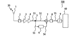
図1は、本実施の形態の無線受信機100のブロック図である。
(First embodiment)
FIG. 1 is a block diagram of
受信機100は、アンテナ1、バンドパスフィルタ2、低雑音増幅器3、段間増幅器4、分
岐器5、遅延器6、乗算器7、ローパスフィルタ8、コンパレータ9、受信データ処理部
60を備える。
The
元の情報が差動符号化された無線信号50をアンテナ1で受信する。
The
バンドパスフィルタ2は無線信号50の干渉波を抑圧して信号帯域を抽出する。
The
バンドパスフィルタ2で抽出した信号を低雑増幅器3と段間増幅器4で増幅して受信信
号51を得る。段間増幅器4は、図1のように1つの増幅器で構成してもよいが、必要に応
じて複数の増幅器を直列接続して構成してもよい。受信信号51の大きさは、以下の(1)
式のように示すことが出来る。
![]()
It can be shown as an equation.
![]()
ここで、tは時間、R51(t)は受信信号51の大きさ、A(t)はフェージング成分を含ん
だ振幅成分、ωは角振動周波数、θ(t)は、差動符号化された位相変調項を示す。受信信
号51は、差動符号化されていれば、位相変調でも周波数変調であっても構わないが、こ
こでは、位相変調の差動符号を用いたDPSK (Differential phase-shift keying)であるも
のとして説明する。
Here, t is time, R 51 (t) is the magnitude of the received
受信信号51は、分岐器5において、受信信号52及び受信信号53に分岐される。受信信
号53は、遅延器6により、1シンボル時間Tの遅延を与えられ、遅延受信信号54となる
。受信信号52の大きさは(2)式のように表すことができる。また、遅延受信信号54の大
きさは(3)式のように表すことが出来る。
![]()
![]()
![]()
![]()
ここで、R102(t)が受信信号52の大きさ、R104(t)が遅延受信信号54の大きさ、αは受信
チェーンの利得(分岐前の受信信号51に対する、分岐された受信信号52の利得)を示して
いる。
Here, R 102 (t) is the magnitude of the received
乗算器7は、受信信号52と1シンボル時間Tの遅延を与えられた遅延受信信号54とを乗
算して出力する。
The
乗算器7の出力から、高調波を除く所望帯域のみがローパスフィルタ8で抽出されて
、遅延検波信号55が得られる。遅延検波信号55は(4)式で表される。

ここで、R55(t)が遅延検波信号55の大きさ、kは受信チェーンの利得と受信信号52
のA(t)、A(t-T)の電力に依存する係数である。また、ωTは2nπ(nは整数値)をとるよ
うに、角振動周波数ωとシンボル時間Tは設定され、(4)式では省略することが出来る。フ
ェージング変動がシンボル時間と比べて緩やかであり、段間増幅器4における増幅が飽和
レベルに近い領域まで受信信号52を増幅していると考えると、kは定数をみなすことが出
来る。
Here, R 55 (t) is the magnitude of the delayed
Is a coefficient depending on the power of A (t) and A (tT). Further, the angular vibration frequency ω and the symbol time T are set so that ωT takes 2nπ (n is an integer value), and can be omitted in the equation (4). Assuming that the fading fluctuation is gentle compared to the symbol time and the amplification in the
遅延検波信号55は、cos[θ(t)-θ(t-T)]に応じて+kから-kまでの値をとるが、コンパ
レータ9において、デジタル情報の“0”か“1”に判定される。コンパレータ9では、
必要に応じて、等価増幅 (Reamplifying)、波形整形 (Reshaping)、時間ジッタ抑圧 (Ret
iming)の処理をも施すようにしてもよい。受信データ処理部60は、コンバレータ9によ
って“0”か“1”に判定されて得られるデジタル信号を元の情報に変換し、例えば音声
に変換したり、種々のアプリケーション処理を行う。
The
If necessary, equivalent amplification (Reamplifying), waveform shaping (Reshaping), time jitter suppression (Ret
iming) may also be performed. The reception
図2は、トランジスタを用いた遅延回路6のブロック図である。
FIG. 2 is a block diagram of the
受信信号53は、AC結合のためのコンデンサ10を介して、トランジスタ11のベース端
子に入力される。
The
トランジスタ11は、エミッタ端子が抵抗18を介して接地されている。また、ベース
端子は、コンデンサ10、抵抗13および14と接続されている。ベース端子には抵抗1
3を介してバイアス電源12が接続される。また、ベース端子は抵抗14を介して接地さ
れる。このように接続されることにより、ベース端子のバイアス条件が決定される。ここ
では、このようにバイアス電源12の電圧を変化させて、バイアス条件を調整する構成と
したが、バイアス条件が可変できる構成であれば、他の回路構成でも構わない。
The emitter terminal of the
3 is connected to the
また、トランジスタ11のコレクタ端子は、VCC電源15に抵抗17を介して接続され
ている。また、受信信号53コレクタ端子に接続されたコンデンサ16を介して、遅延受
信信号54が出力される。
The collector terminal of the
なお、図2においては、入力側負荷及び出力側負荷は、説明の簡単化のため省略してい
るが、例えば入力側負荷を介して受信信号53をコンデンサ10へ入力するよう構成して
もよい。また、コンデンサ16から出力側負荷を介して遅延受信信号54を出力するように
構成してもよい。
In FIG. 2, the input side load and the output side load are omitted for simplification of description, but the
ここで、遅延受信信号54は、トランジスタ11によって受信信号53に対して群遅延τ
を被ることになる。また、遅延受信信号54の位相は、トランジスタ11に与えられるバイ
アス電源12によって決定されるバイアス条件に応じて回転する特徴がある。従って、遅
延受信信号54は、(5)式のように表すことが出来る。
![]()
Will suffer. Further, the phase of the delayed
![]()
ここで、R54'(t)が遅延受信信号54の大きさ、τはトランジスタ11による群遅延量、
φVbiasはトランジスタ11のバイアス条件Vbiasに依存して回転する位相量を示す。遅延
検波の理想条件としては、τ = Tであり、φVbiasが、2mπ(mは整数)である。但し、ト
ランジスタ11の群遅延τは、理想条件から外れている場合が考えられ、遅延検波信号5
5は、(6)式のように表すことができる。
φ Vbias indicates a phase amount that rotates depending on the bias condition Vbias of the
5 can be expressed as in equation (6).
ここで、R55'(t)が遅延検波信号55の大きさである。受信信号52は、段間増幅器4
により飽和レベル近くまで増幅されたこと、フェージングの影響による変動がシンボル時
間に比較して緩やかであることを考慮すると、kは(4)式と同様の数値をとると考えら
れる。群遅延τはバイアス電源12に応じて変化することが考えられるが、絶対遅延時間
としては変化が微小とみなすことができるので、一定であるとして考えられる。(6)式
中のωτは(7)式のように表すことができる。
![]()
In consideration of the fact that the signal is amplified to near the saturation level and the fluctuation due to the fading is gradual compared to the symbol time, k is considered to take the same numerical value as in the equation (4). The group delay τ can be considered to change according to the
![]()
ここで、γはτ/Tであり、τ≒Tであれば、ωτ≒ 2πとして無視できる。また、位相
変調項であるθ(t)-θ(t-τ)もτ≒Tであれば、差動符号として、0 あるいは πの値をと
ることになる。従って、位相項であるφVbiasの設定を考えて、バイアス電源12を調整
すれば良い。バイアス電源12は、遅延受信信号54がトランジスタ11から被った位相回
転量が2・n・π(nは整数)、あるいは、2・(n+1)・π(nは整数)となるように設定する。
Here, γ is τ / T. If τ≈T, it can be ignored as ωτ≈2π. If the phase modulation term θ (t) −θ (t−τ) is also τ≈T, the differential code takes a value of 0 or π. Therefore, the
位相項φVbias = 2・(n+1)・πの場合は、変調項θ(t)-θ(t-T)に対して、遅延検波信
号55の出力の正負が反転することになる。
In the case of the phase term φ Vbias = 2 · (n + 1) · π, the sign of the output of the delayed
遅延検波信号55の反転は、以下の方法で簡易に補完することが可能である。例えば、
通信接続の開始時に、受信機100にとって既知信号を、送信機側から受信機100側に
送信する。受信機100はその既知信号を受信して遅延処理した遅延検波信号55と既知
信号とを比較することで符号が反転しているか否かを判断することが可能となる。符号が
反転している場合には、受信機100側において、コンパレータ9の後段において、イン
バータを挿入して、元に戻すことが可能であり、無線通信システムにおいては、符号の反
転が発生しても、補完することが可能であり、問題とはならない。
Inversion of the delayed
At the start of communication connection, a signal known to the
図3に、トランジスタ11における、バイアス電源12に対する位相回転量の特性を示
す。図3のグラフは、図2のトランジスタ11を使った回路において、横軸にバイアス電
源12の電圧をとり、縦軸は、遅延受信信号54における受信信号53に対する相対位相差
φVbias [degree] (S21特性のphase) を示している。但し、トランジスタ11で発生する
群遅延量はここでは既知として除いている。図3は、図2の回路構成において、トランジ
スタに2SCタイプを用いて、Vcc = 5 Vとして、Vbiasを0〜5.0 Vまで可変させた際の所定
の周波数帯における位相特性である。トランジスタ11は、ベース側の電流条件が、バイ
アス電圧VVbiasに依存して変化し、トランジスタ11の入出力間(エミッタ‐ベース、ベ
ース‐コレクタ、コレクタ‐エミッタ)で容量結合している値が変動して位相回転量が変
化することになる。図2の回路は反転増幅器の構成であり、バイアス電源12がVCCに比
べて十分抑えられて、トランジスタがOn状態となっている場合は、位相回転量はπ(18
0度)で安定するが、バイアス電源12がトランジスタ11のしきい値付近の(バイアス
電源12がVCCに比べてさほど小さくなくなる)エリアにおいては、指数的に位相回転量
が変動することになる。このような位相変化は、使用するトランジスタと透過させる信号
の周波数の関係に依存する。一般的には、トランジスタの動作状態が、ベースに流れる電
流あるいは印加される電圧に依存して切り替わる際に位相が大きく回る。このようなトラ
ンジスタ11の位相変化の原理特性を、遅延回路6の位相調整に活用する。図2の回路構
成では、コレクタ側から遅延受信信号54を出力しているため反転増幅タイプとなるが、エ
ミッタ側から遅延受信信号54を出力して、非反転増幅タイプとしても構わない。また、ト
ランジスタは、バイポーラあるいはFETのどちらのタイプでもよく、NPN、PNP、NMOS、PMO
Sの極性も回路構成やプロセスにあわせて選択してよい。
FIG. 3 shows the characteristics of the phase rotation amount with respect to the
However, in the area where the
The polarity of S may be selected according to the circuit configuration and process.
図2に示す回路構成を用いて、バイアス電源12が出力する電圧としてバイアス電圧VVbi
asを設定して位相量φVbiasを調整する場合、バイアス電圧VVbiasの設定ターゲットが必
要となる。図4において、位相量φVbiasを調整するための回路構成を示し、回路動作を
説明する。
Using the circuit configuration shown in FIG. 2, the bias voltage V Vbi is used as the voltage output from the
When adjusting the phase amount φ Vbias by setting as , a setting target for the bias voltage V Vbias is required. In FIG. 4, a circuit configuration for adjusting the phase amount φ Vbias is shown, and the circuit operation will be described.
図4は、分岐器43、レベル検出器40、微分器41、ループフィルタ42から構成さ
れるバイアス電圧VVbiasの制御回路を、図1のブロック図に追加した構成を示す図である
。分岐器43において、図1における遅延検波信号55の一部を制御回路側に分岐する。
FIG. 4 is a diagram showing a configuration in which a control circuit for the bias voltage V Vbias composed of the branching
遅延検波信号55は、レベル検出器40で、信号振幅レベルを検出される。レベル検出器
40は例えば図9や図10に示すような、ダイオード44とコンデンサ45との組み合わ
せによって実現することができる。
The delayed
図9では、遅延検波信号55はダイオード44へ順方向に入力されて負の成分がカット
される。ダイオード44の出力端は抵抗46を介して、一端が接地されたコンデンサ45
の他端に接続されている。コンデンサ45の他端から振幅レベル出力56が取り出される
。
In FIG. 9, the delayed
Is connected to the other end. An
また、図10では、ダイオード144が抵抗146の一端から逆方向に接地されている
。コンデンサ145は一端が抵抗146の他端に接続し、他端が接地されている。抵抗1
46の一端から遅延検波信号55が入力され、他端から振幅レベル出力56が取り出され
る。
In FIG. 10, the diode 144 is grounded in the reverse direction from one end of the
A
信号振幅レベル出力56は、図4中の(a)に示されているように、位相項φVbiasに依存
した周期関数となる。位相項φVbiasが0 あるいは πであれば、遅延検波出力である遅
延受信信号54は、最大振幅をとることとなる。また、逆に、位相項φVbiasが±π/2 で
あると、受信信号52と受信信号53が直交の関係となり、出力レベルは原理上、ゼロと
なる。遅延回路6におけるバイアス電源12は、(a)のグラフにおいて出力レベルが最
大となるように調整すれば良い。図4においては、信号振幅レベル出力56を微分回路2
0で一回微分し、ループフィルタ42を通して、図4中(b)に示す位相項φVbiasとル
ープフィルタ出力57の関係を得る。ここで、図4中(b)の丸印のゼロクロスポイント
を用いて、バイアス電圧VVbiasを制御することが可能となる。ループフィルタ出力57が
プラスの数値を出力していれば、バイアス電圧VVbiasを大きくして位相項φVbiasをすす
める方向とし、逆にループフィルタ出力57がマイナスの数値を出力していれば、バイア
ス電圧VVbiasを小さくして位相項φVbiasを遅らせる方向とすれば良い。なお、図2にお
いてトランジスタ11をNPN型として表記したためここではバイアス電圧VVbiasと位相項
φVbiasとの増加および減少の関係を上記のように説明したが、トランジスタ11をPN
P型の極性のものにすれば逆の関係となることは言うまでもない。
The signal
Differentiation is performed once at 0, and the relationship between the phase term φ Vbias and the
Needless to say, if the P-type polarity is used, the relationship is reversed.
ループフィルタ出力57は直接、バイアス電源12が供給するバイアス電圧として印加
する設計としてもよい。あるいはループフィルタ出力57に所定のリファレンス電圧を加
算、あるいは減算して、バイアス電源12として遅延回路6へ供給する設計とするなど、
ループフィルタ出力57に依存したバイアス電圧をバイアス電源12が供給することにし
てもよい。
The
The
遅延受信信号54は、位相項φVbiasに依存して符号の正負が反転する場合があるが、無線
通信の接続開始時の既知情報を用いて、デジタル信号処理により反転を戻すことは可能で
ある。図4においては、分岐された遅延検波信号55を、レベル検出器40を通さずに微
分回路41に入力するようにしてもよい。その際には、同様に、既知信号として、符号が
どちらか一方に1連続などのように固定されている情報を送信機から出力し、これを無線
信号50として受信して遅延検波信号55を生成するとよい。
Depending on the phase term φ Vbias , the sign of the delayed received
図2に示す回路構成において、トランジスタの群遅延のみを利用して安定した遅延検波
が可能であれば(すなわち位相項φVbiasの動的な調整が不要であれば)、バイアス電圧V
Vbiasは固定して、位相制御は施さなくても構わない。また、バイアス電圧VVbiasによる
位相項φVbiasの制御においては、トランジスタ11による利得の特性も変化することに
なる。利得の変動に対しては、図2の回路の前段、あるいは後段に、利得補償用の増幅器
を挿入して利得補完する構成や、飽和レベルまで増幅するようなリミッタを挿入する構成
等により、遅延させた遅延受信信号54の強度を安定させる手段との組み合わせも考えら
れる。
In the circuit configuration shown in FIG. 2, if stable delay detection is possible using only the group delay of the transistors (that is, if dynamic adjustment of the phase term φ Vbias is unnecessary), the bias voltage V
Vbias may be fixed and phase control may not be performed. Further, in the control of the phase term phi Vbias from the bias voltage V Vbias, it will also vary the gain characteristic due to the
図4の制御回路においては、いくつかの動作方式が考えられる。 In the control circuit of FIG. 4, several operation methods can be considered.
ループフィルタ42の通過帯域をデータ速度に比べて十分に広くした構成であれば、通信
接続を開始する際に送信機側から送られてくる既知信号(例えばプリアンブル等)を受信
している間にバイアス電圧VVbiasを設定し、既知信号の受信を終えてデータ信号を受信す
る際にはバイアス電圧VVbiasを既知信号により設定した値に固定して位相項φVbiasが動
かないようにすればよい。
If the configuration is such that the pass band of the
ループフィルタ42の帯域をデータ速度に比べて十分に狭くし、遅延検波信号55のう
ちビット単位のデータ系列で表された部分がバイアス電圧VVbiasの調整に供されない構成
であれば、レベル検出回路19をバイパスさせて以下のような方法でバイアス電圧VVbias
を設定する。
If the band of the
Set.
遅延検波信号55はレベル検出回路19を通らずにループフィルタ42に入力する。こ
の場合、ループフィルタ42に入力される信号は電圧値として正負両方値をとることとな
る。その場合、遅延検波信号55のうちビット単位のデータ系列で表された部分の−1デ
ータの数と+1データの数とが同じずつであると、その部分のデータの平均は0となって
しまう。すなわち、−1データや+1データに相当する遅延検波信号55の電圧値の絶対
値がいくら大きくても、ループフィルタ42を通過する値はあまり大きくならない。
The delayed
それを避けるために、無線受信機100が受信する無線信号50を送信する送信機にお
いて、遅延検波信号55のうちビット単位のデータ系列で表された部分の差動符号化θ(t
)-θ(t-τ)において、データ0 (θ(t)-θ(t-τ) = -π)と1 (θ(t)-θ(t-τ) = π)
の発生確率を、“1”のマーク率が高いように設定する。このようなデータ系列とするこ
とで、データ系列中の平均値が0からより外れた値となるので、帯域が狭いループフィル
タ42の出力も0から外れる。その結果、ループフィルタ出力57の大小が判定できるの
で、上述のように図4(a)中における位相項φVbiasと出力レベルの関係から、位相項φ
Vbias = πとなる条件に、バイアス電源12を設定することができるようになる。
In order to avoid this, in the transmitter that transmits the
) -θ (t-τ), data 0 (θ (t) -θ (t-τ) = -π) and 1 (θ (t) -θ (t-τ) = π)
Is set so that the mark rate of “1” is high. By adopting such a data series, the average value in the data series becomes a value deviating from 0, so that the output of the
The
伝送情報が画像情報のようなストリーミングであれば、データ情報をフレーム化し、そ
のフレームヘッダ部分において“1”のマーク率を高めたデータ系列としてもよい。ある
いはマーク率が高いダミーブロックをフレームに挿入してもよい。
If the transmission information is streaming such as image information, the data information may be framed and a data series in which the mark rate of “1” is increased in the frame header portion. Alternatively, a dummy block having a high mark rate may be inserted into the frame.
勿論、上記以外の制御回路の動作方法でも、バイアス電圧VVbiasを制御して、位相項φ
Vbias調整し、遅延受信信号54が最大振幅レベルとなるような構成であれば、構わない
。
Of course, the operation of the control circuit other than the above also controls the bias voltage V Vbias and the phase term φ
Any configuration may be used as long as Vbias adjustment is performed and the delayed
(変形例)
バイアス電圧VVbiasによる位相項φVbiasの調整条件は、トランジスタ11への入力信号
である受信信号53の周波数に依存する。すなわち、高周波においては、トランジスタ1
1の入力および出力における容量結合にも依存して、位相が回転しきらず、位相回転量と
してπを得られないこともある。受信信号53が高周波であっても十分な位相回転量を得
るためには、トランジスタ11を多段接続して遅延回路6を構成してもよい。
(Modification)
Adjusting the conditions of the phase term phi Vbias from the bias voltage V Vbias depends on the frequency of the received
Depending on the capacitive coupling at the input and output of 1, the phase may not be fully rotated and π may not be obtained as the amount of phase rotation. In order to obtain a sufficient amount of phase rotation even when the
図5は、トランジスタ11を3段接続して実現した遅延回路6の一実施形態としての回
路図である。
FIG. 5 is a circuit diagram as an embodiment of the
受信信号53は、AC結合のためのコンデンサ10を介して、1段目のトランジスタ1
1のベース端子に入力される。
The
1 to the base terminal.
1段目のトランジスタ11は、エミッタ端子が抵抗18を介して接地されている。また
、ベース端子は、コンデンサ10、抵抗13および14と接続されている。ベース端子に
は抵抗13を介してバイアス電源12が接続される。また、ベース端子は抵抗14を介し
て接地される。トランジスタ11のコレクタ端子は、インダクタ19を介してVCC電源1
5に接続された抵抗17から、VCC電圧が供給される。また、コレクタ端子はコンデンサ
16を介して2段目のトランジスタ21のベース端子に接続されている。
In the
A V CC voltage is supplied from a
2段目のトランジスタ21は、エミッタ端子が抵抗28を介して接地されている。また
、ベース端子は、コンデンサ16、抵抗23および24と接続されている。ベース端子に
は、インダクタ29を介してバイアス電源12に接続された抵抗23から、バイアス電圧
が供給される。また、ベース端子は抵抗24を介して接地される。トランジスタ21のコ
レクタ端子は、VCC電源15に抵抗27を介して接続されている。また、コレクタ端子は
コンデンサ26を介して3段目のトランジスタ31のベース端子に接続されている。
The emitter terminal of the
3段目のトランジスタ31は、エミッタ端子が抵抗38を介して接地されている。また
、ベース端子は、コンデンサ26、抵抗33および34と接続されている。ベース端子に
は、インダクタ29とインダクタ39とを介してバイアス電源12に接続された抵抗33
から、バイアス電圧が供給される。また、ベース端子は抵抗34を介して接地される。ト
ランジスタ31のコレクタ端子は、VCC電源15にインダクタ49を介して接続された抵
抗37からVCC電圧を供給されている。また、コレクタ端子に接続されたコンデンサ46
を介して遅延受信信号54が出力される。
The
From the above, a bias voltage is supplied. The base terminal is grounded via the
The delayed
VCC及びVbiasは各段で共通としているが、各段のアイソレーションを高めるために、段
間にはインダクタ19、29、39及び49を挿入している。
Although V CC and Vbias are common to each stage,
各段において、位相変化量がβ [radian]であれば、3段接続することで、3×β [radia
n] の位相変化量が得られることになる。多段とすることで、受信信号53に対して遅延
受信信号54は増幅されることになるが、たとえ、飽和状態に近い領域まで増幅されても、
2値 あるいは 4値の位相変調、あるいは周波数変調であれば、振幅成分が平坦となって
も、位相あるいは周波数成分に情報が残っているので、復調機能においては問題にならな
い。また逆に、飽和レベルに近い領域で、受信信号53を遅延受信信号54として伝達する
ことで、出力レベルが安定した遅延検波信号55遅延検波信号55を得られることになる
。通常、トランジスタを1段とした図2の場合、反転増幅が理想的な状態であり位相回転
量としてはπ [radian]までである。遅延検波のためには、位相回転量として、2×π [ra
dian]の自由度が必要であり、2段あるいは3段の多段接続とすることが望ましい。トラン
ジスタ11を用いた回路の段数としては、位相調整という機能を考慮すると、2個以上で
あれば、2×π [radian]を提供することが可能である。
If the amount of phase change is β [radian] at each stage, connecting 3 stages will result in 3 × β [radia
n] is obtained. By using multiple stages, the delayed received
In the case of binary or quaternary phase modulation or frequency modulation, even if the amplitude component becomes flat, information remains in the phase or frequency component, so there is no problem in the demodulation function. Conversely, by transmitting the
dian] is required, and it is desirable to use a multistage connection of two or three stages. If the number of stages of the circuit using the
以上、第1の実施例について述べてきたが、図1から図5に示した回路は、全て半導体
素子で実装することが可能である。遅延回路としても、従来のように物理的な伝搬路長が
必要なく、トランジスタの群遅延を利用しており、また、遅延受信信号54の位相調整も
トランジスタのバイアス電源の条件を変更することで可能である。したがって、本発明の
第1の実施例である図1から図5の回路は、集積回路としてワンチップ内に全て実装して
、遅延検波の機能を提供することが可能となる。
Although the first embodiment has been described above, the circuits shown in FIGS. 1 to 5 can all be mounted with semiconductor elements. The delay circuit does not require a physical propagation path length as in the prior art, uses the group delay of the transistor, and also adjusts the phase of the delay received
(第2の実施の形態)
図6を用いて、第2の実施形態について説明する。第1の実施の形態においては、トラ
ンジスタを用いた遅延器6の出力を用いた遅延検波を行う構成について述べたが、同期検
波にも適用することが可能である。
(Second Embodiment)
The second embodiment will be described with reference to FIG. In the first embodiment, the configuration for performing the delay detection using the output of the
図6は、同期検波用のローカル信号に本発明を用いた、本実施の形態の無線受信機20
0のブロック図である。
FIG. 6 shows a
It is a block diagram of 0.
受信機200は、アンテナ201、バンドパスフィルタ202、低雑音増幅器203、段
間増幅器204、分岐器205、遅延器206、乗算器207、ローパスフィルタ208
、コンパレータ209、レベル検出器240、微分器241、ループフィルタ242、分
岐器243、ローカル信号発生器222およびシンセサイザ223を備える。
The
A
2値のBinary phase-shift keying (BPSK)の変調方式で変調されている無線信号25
0をアンテナ201で受信する。無線信号250を、バンドパスフィルタ202、低雑音
増幅器203、段間増幅器204を通して受信信号251を得る。
Radio signal 25 modulated by binary binary phase-shift keying (BPSK) modulation method
0 is received by the
分岐器205において分岐させた受信信号251の一部を、ローカル信号発生器222が
発生するローカル信号の周波数をロック(同期)するためのシンセサイザ223に入力す
る。受信信号251と周波数同期されたローカル信号258は、遅延器206で群遅延を与
えられて、乗算器207に入力される。乗算器207では、分岐器205からの受信信号
251とローカル信号258をミキシングして、同期検波を行う。同期検波を施された受信
信号を、所望帯域を抽出するローパスフィルタ208を通して、復調信号259を得る。
A part of the
復調信号259は、コンパレータ209において“0” あるいは “1”に判定される。
The
ここで、復調信号259は、(8)式のように表すことができる。
ここで、R109(t)は復調信号259の大きさ、LPF8[・・・]は、所望帯域を抽出するロ
ーパスフィルタ機能、つまり[ ]内の式で得られる解のうち所望帯域以上の値を制限する
ことを示している。また、αは受信チェーンの利得、Aは無線信号250の振幅、ωは無
線信号250の角振動周波数、θ(t)は無線信号250の位相変調項(0 あるいは π)、
φVbiasはローカル信号258の位相項を示している。
Here, R 109 (t) is the size of the
φ Vbias indicates the phase term of the
無線信号250はBPSK変調であるため、ローカル信号258の位相項であるφVbiasが受信
信号251に対する相対位相としてnπ(nは整数)であれば、受信感度を劣化させずに復
調することが可能となる。
Since the
定数nが奇数の場合は符号が反転することになるが、それは既知情報を使ってコンパレ
ータ209よりも後段のデジタル信号処理部において反転することが可能である。
When the constant n is an odd number, the sign is inverted. However, it can be inverted in the digital signal processing unit subsequent to the
従って、ローカル信号258の位相を遅延させる遅延器206は、復調信号259のレベ
ルが最大となるように機能させればよい。遅延器206の位相を調整する制御回路は、図
4に示した構成と同様であり、レベル検出器240、微分器241、ローパスフィルタ242
で構成することができる。すなわち、ローパスフィルタ208の後段に設ける分岐器243
から、復調信号259の一部を分岐して取り出し、レベル検出器240に入力させる。そ
して、レベル検出器240の出力が最大となるように、遅延器206の位相を調整する。
Therefore, the
Can be configured. That is, the branching
From this, a part of the
この調整の仕方については、図4の説明と同様であるため省略する。 This adjustment method is the same as that described in FIG.
本実施の形態においては、DPSK方式の位相変調に対し1シンボル時間の遅延を与える構
成について説明した。トランジスタが与える群遅延の大きさ次第で、1シンボル時間のみ
の遅延ではなく、mシンボル(mは2以上の実数)の遅延を与える構成も可能である。その
際には、送信機側で、mシンボル遅延の符号化を行うことで、1シンボル遅延の復調と同
じ受信感度が得られることになる。通常、mシンボル遅延のmが大きくなるとフェージング
の影響が強く出てきて、シンボル間の相関が弱まる可能性がある。しかしながら、60 GHz
帯ミリ波を用いた無線通信システムにおいては、近距離での通信でもあり、またLOS(Lin
e of Sight)が基本となることが多いので、mが大きくなっても受信感度には大きな影響
はないと考えられる。遅延させるシンボル長の設定は、使用するトランジスタ、RF周波数
帯、ビットレートの兼ね合いから決定すればよい。
In the present embodiment, a configuration has been described in which a delay of one symbol time is provided for DPSK phase modulation. Depending on the size of the group delay provided by the transistor, a configuration in which a delay of not more than one symbol time but m symbols (m is a real number of 2 or more) is also possible. In that case, the same reception sensitivity as that of demodulation of 1 symbol delay can be obtained by encoding m symbol delay on the transmitter side. Normally, when m of the m symbol delay increases, the influence of fading becomes strong and the correlation between symbols may be weakened. However, 60 GHz
In wireless communication systems using millimeter-wave, it is also a short-range communication, and LOS (Lin
e of Sight) is often the basis, so even if m increases, it is considered that there is no significant effect on reception sensitivity. The setting of the symbol length to be delayed may be determined based on the balance between the transistor to be used, the RF frequency band, and the bit rate.
(第3の実施の形態)
図7を用いて、本発明の第3の実施形態について説明する。
(Third embodiment)
A third embodiment of the present invention will be described with reference to FIG.
上記実施の形態では受信機に本発明を適用した構成を示したが、本実施の形態では送信機
に適用した構成について説明する。
In the above embodiment, a configuration in which the present invention is applied to a receiver is shown, but in this embodiment, a configuration applied to a transmitter will be described.
本実施の形態の送信機300は、変調方式にBPSKを用いた変調信号に、位相制御を施し
たローカル信号を重畳した送信信号を送信する。受信機側ではローカル信号などは用いず
、二乗検波などの簡易な構成で復調する構成である。本構成であれば、第2の実施の形態
で用いたシンセサイザが不必要となるため、送信機及び受信機を含めた無線通信システム
として、簡易な構成になる利点がある。特にシンセサイザは、ミリ波などの60GHz付近の
高周波においては実装が困難であるため、削除できる利点は大きい。
図7は、重畳するローカル信号の位相調整に本発明を用いた、本実施の形態の無線送信
機300のブロック図である。
FIG. 7 is a block diagram of a
送信機300は、アンテナ301、バンドパスフィルタ302、パワーアンプ303、段
間増幅器304、分岐器305、遅延器306、乗算器307、バンドパスフィルタ30
8、加算器309、レベル検出器340、微分器341、ループフィルタ342、分岐器
343、ローカル信号発生器322および送信データ生成部320を備える。
The
8, an
送信データ生成部320はデータ“0” あるいは “1”を、BPSKの送信データ用に“
−1” あるいは “+1”に符号化した送信データ信号(ベースバンド信号)350を出力
する。
The transmission
A transmission data signal (baseband signal) 350 encoded to “−1” or “+1” is output.
送信データ信号350は、ローカル信号発生器322から出力され分岐器343にて分
岐されたローカル信号358の一部と、乗算器307においてミキシングされ、所望のRF帯
域に周波数アップコンバートされたRF信号361となる。
The transmission data signal 350 is a part of the
RF信号361は両側波帯にデータ情報が存在しているが、バンドパスフィルタ308で
片側の側波帯だけを抽出する。但し、このバンドパスフィルタ308では、両側波帯とも
通過させても復調は可能である。ここでは片側波帯を通過させて伝送するものとして説明
する。RF信号361は、加算器309において、遅延器306で位相制御された遅延ロー
カル信号354と加算されて、送信信号352となる。送信信号352は、(9)式のよ
うに表すことができる。
![]()
![]()
ここで、T352(t)は送信信号352の大きさ、Aは送信信号352の振幅、θ(t)は位
相変調項 (0 あるいは πの値をとる)であり、ωはRF帯の角振動周波数、φVbiasはロ
ーカル信号358に遅延器306が与えた位相の変化量を表す項すなわち変調信号A・cos
{θ(t)}・cos(ωt)に対する相対位相を示している。
Where T 352 (t) is the magnitude of the
The relative phase with respect to {θ (t)} · cos (ωt) is shown.
送信信号352は、段間増幅器304、パワーアンプ303において増幅され、バンド
パスフィルタ302を通過してアンテナ301から無線信号351として送信される。こ
こで、加算器309の後段に分配器305を挿入し、送信信号352の一部を位相制御回
路に入力して、遅延器306でローカル信号358に与える位相量(つまり(9)式にお
ける位相項φVbiasの値)を調整する。この位相制御回路は、図4に示した構成と同様で
あり、レベル検出器340、微分器341、ローパスフィルタ342で構成することがで
きる。制御回路は、送信信号352の一部をレベル検出器340に入力し、そのレベル検
出器340の出力が最大となるように、遅延回路306の位相を制御することになる。制
御機能については、図4の説明において述べているため省略する。レベル検出器340が
例えば図9や図10のような包絡線検波を行う構成であれば、レベル検出器340の出力
である振幅レベル出力356は(10)式のように表すことができる。
ここで、T356’(t)は振幅レベル出力356である。振幅レベル出力356が最大と
なるためには、位相項φVbiasは、nπ(nは整数)であることが望ましい。
Here, T 356 ′ (t) is the
以上説明した送信機300からの無線信号351を受信する受信機400の構成の一例
を図8を用いて説明する。 受信機400は、アンテナ401、バンドパスフィルタ40
2、低雑音増幅器403、段間増幅器404、レベル検出器440、ローパスフィルタ4
08及びコンパレータ409を備える。
An example of the configuration of the
2,
08 and a
送信機300から送信されアンテナ401で受信した無線信号351は、パンドパスフ
ィルタ402、低雑音増幅器403、段間増幅器404を介して、レベル検出器440に
受信信号451として入力される。レベル検出器440は、図7のレベル検出器340と
同様の構成のものを用いることができる。レベル検出器440の出力である振幅レベル出
力456の所望帯域のみをローパスフィルタ8で抽出して検波信号455は、式(10)
で記載されたレベル検出器340の出力と等価(すなわちほぼ相似)となる。従って、検
波信号455のレベルが最大となるように、位相項φVbiasを調整することが望ましく、
位相項φVbias = nπ(nは整数)の関係が確保できれば、受信感度の劣化をおこすこと
なく復調することが可能となる。
A
Is equivalent (ie, substantially similar) to the output of the
If the relationship of the phase term φ Vbias = nπ (n is an integer) can be ensured, it is possible to perform demodulation without deteriorating reception sensitivity.
検波信号455は、コンパレータ409で、第1の実施形態の同様に、データ“0” あ
るいは “1”のデジタル信号に復調されることになる。定数nが奇数の場合は符号が反転
することになるが、それは既知情報を使ってコンパレータ409後段のデジタル信号処理
部において簡便に反転することが可能である。
The
ローカル信号発生器322は、受信信号451に対して周波数をロックしてもよいが、
ロックしていなくても、通信機能としては問題なく、シンセサイザを省くことが可能であ
る。つまり、本実施の形態では、送信機側及び受信機側において、デジタル信号による位
相変調であるBPSK方式を用いていながら、シンセサイザは必要なく、また受信機側ではロ
ーカル信号が不要となる利点がある。また、これらの送信機及び受信機は、全て半導体素
子で構成することが可能であるため、ワンチップICへの集積化が容易となる利点がある。
The
Even if it is not locked, there is no problem with the communication function and the synthesizer can be omitted. That is, in this embodiment, there is an advantage that a synthesizer is not necessary on the transmitter side and the receiver side, and a synthesizer is not necessary, and a local signal is not necessary on the receiver side. . Moreover, since these transmitters and receivers can all be composed of semiconductor elements, there is an advantage that integration into a one-chip IC is easy.
なお、本発明は上記実施の形態そのままに限定されるものではなく、実施段階ではその
要旨を逸脱しない範囲で構成要素を変形して具体化できる。例えば既に触れたように、極
性の異なるトランジスタを用いることは可能であることは言うまでもない。また、上記実
施の形態に開示されている複数の構成要素の適宜な組み合わせにより、種々の発明を形成
できる。例えば、実施の形態に示される全構成要素から幾つかの構成要素を削除してもよ
い。さらに、異なる実施の形態にわたる構成要素を適宜組み合わせてもよい。
Note that the present invention is not limited to the above-described embodiment as it is, and can be embodied by modifying the components without departing from the scope of the invention in the implementation stage. For example, as already mentioned, it is needless to say that transistors having different polarities can be used. Various inventions can be formed by appropriately combining a plurality of constituent elements disclosed in the embodiments. For example, some components may be deleted from all the components shown in the embodiment. Furthermore, constituent elements over different embodiments may be appropriately combined.
1,201,301,401・・・アンテナ、2,202,302,402・・・バンドパスフィルタ、3,203・・・
低雑音増幅器、4,204,304,404・・・段間増幅器、5,205,305・・・分岐器、6,206,306・
・・遅延器、7,207,307・・・乗算器、8,208,408・・・ローパスフィルタ、9,209,409・
・・コンパレータ、10,210,310・・・コンデンサ、11,211,311・・・トランジスタ、12,2
12,312・・・バイアス電源、13,213,313・・・抵抗、14,214,314・・・抵抗、15,215,315
・・・VCC電源、16,216,316・・・コンデンサ、17,217,317・・・抵抗、18,218,318・・
・抵抗、19,219,319・・・インダクタ、20・・・コンデンサ、21・・・トランジスタ、23
・・・抵抗、24・・・抵抗、26・・・コンデンサ、27・・・抵抗、28・・・抵抗、29・・
・インダクタ、30・・・コンデンサ、31・・・トランジスタ、33・・・抵抗、34・・・抵
抗、36・・・コンデンサ、37・・・抵抗、38・・・抵抗、39・・・インダクタ、40,240,3
40,440・・・レベル検出器、41,241,341・・・微分器、42,242・・・ループフィルタ、43
,243,343・・・分岐器、44,144・・・ダイオード、45,145・・・コンデンサ、46,146・・
・抵抗、50,250,351・・・無線信号、51,251,451・・・受信信号、52・・・受信信号、53
・・・受信信号、54・・・遅延受信信号、55・・・遅延検波信号、56,256,356,456・・
・振幅レベル出力、57,257・・・ループフィルタ出力、58,258,358・・・ローカル信号、
59,259・・・復調信号、60,460・・・受信データ処理部、100,200,300,400・・・受信機
、222322・・・ローカル信号発生器、223・・・シンセサイザ、303・・・パワーアンプ、
308・・・バンドパスフィルタ、309・・・加算器、320・・・送信データ生成部、350・・
・送信データ、352・・・送信信号、354・・・遅延ローカル信号、361・・・RF信号、45
5・・・検波信号。
1,201,301,401 ... antenna, 2,202,302,402 ... bandpass filter, 3,203 ...
Low noise amplifier, 4,204,304,404 ... Interstage amplifier, 5,205,305 ... Branch, 6,206,306 ・
..Delayer, 7,207,307 ... Multiplier, 8,208,408 ... Low pass filter, 9,209,409
..Comparator, 10,210,310 ... Capacitor, 11,211,311 ... Transistor, 12,2
12,312 ... Bias power supply, 13,213,313 ... Resistance, 14,214,314 ... Resistance, 15,215,315
... VCC power supply, 16,216,316 ... Capacitor, 17,217,317 ... Resistance, 18,218,318 ...
・ Resistance 19,219,319 ・ ・ ・
... Resistance, 24 ... Resistance, 26 ... Capacitor, 27 ... Resistance, 28 ... Resistance, 29 ...
Inductor, 30 ... capacitor, 31 ... transistor, 33 ... resistor, 34 ... resistor, 36 ... capacitor, 37 ... resistor, 38 ... resistor, 39 ... inductor , 40,240,3
40,440 ... level detector, 41,241,341 ... differentiator, 42,242 ... loop filter, 43
, 243,343 ... Branch, 44,144 ... Diode, 45,145 ... Capacitor, 46,146
・ Resistance, 50,250,351 ... Radio signal, 51,251,451 ... Received signal, 52 ... Received signal, 53
... Received signal, 54 ... Delayed received signal, 55 ... Delayed detection signal, 56,256,356,456 ...
Amplitude level output, 57,257 ... Loop filter output, 58,258,358 ... Local signal,
59,259 ... demodulated signal, 60,460 ... received data processing unit, 100, 200, 300, 400 ... receiver, 222322 ... local signal generator, 223 ... synthesizer, 303 ... power amplifier,
308 ... Band pass filter, 309 ... Adder, 320 ... Transmission data generator, 350 ...
・ Transmission data, 352 ... Transmission signal, 354 ... Delayed local signal, 361 ... RF signal, 45
5: Detection signal.
Claims (16)
前記第1の分岐入力信号の位相を遅延させるトランジスタと、
前記第2の分岐入力信号に、位相を遅延した前記第1の分岐入力信号を乗算する乗算手
段と、
を備えることを特徴とする遅延検波回路。 Distributing means for distributing the input signal to the first branch input signal and the second branch input signal;
A transistor for delaying the phase of the first branch input signal;
Multiplying means for multiplying the second branch input signal by the first branch input signal delayed in phase;
A delay detection circuit comprising:
号の位相を遅延させる量を制御するバイアス電圧付与手段を備えることを特徴とする請求
項1記載の遅延検波回路。 2. The delay detection circuit according to claim 1, further comprising bias voltage applying means for controlling an amount of delaying the phase of the first branch input signal by controlling a bias voltage applied to the transistor.
ることにより、前記第1の分岐入力信号の位相の遅延させる量を増加させることを特徴と
する請求項1記載の遅延検波回路。 2. The delay detection circuit according to claim 1, wherein the bias voltage applying means increases an amount of delay of the phase of the first branch input signal by increasing an absolute value of a bias applied to the transistor. .
前記第1の分岐入力信号を入力する前記トランジスタのベース端子に、バイアス電圧を
印加するバイアス電圧付与手段を備えることを特徴とする請求項1記載の遅延検波回路。 The transistor is a bipolar type,
2. The delay detection circuit according to claim 1, further comprising bias voltage applying means for applying a bias voltage to a base terminal of the transistor to which the first branch input signal is input.
相を遅延した前記第1の分岐入力信号を得ることを特徴とする請求項4記載の遅延検波回
路。 5. The delay detection circuit according to claim 4, wherein an emitter terminal of the transistor is grounded, and the first branch input signal having a phase delayed from the collector terminal of the transistor is obtained.
前記第1の分岐入力信号が入力される前記トランジスタのソース端子に、バイアス電圧
を印加するバイアス電圧付与手段を備えることを特徴とする請求項1記載の遅延検波回路
。 The transistor is a FET type,
2. The delay detection circuit according to claim 1, further comprising bias voltage applying means for applying a bias voltage to a source terminal of the transistor to which the first branch input signal is input.
の分岐入力信号を得ることを特徴とする請求項6記載の遅延検波回路。 The gate terminal of the transistor is grounded and the first phase is delayed from the drain terminal.
7. The delay detection circuit according to claim 6, wherein a branch input signal is obtained.
トランジスタを備えることを特徴とする請求項1記載の遅延検波回路。 The delay detection circuit according to claim 1, further comprising: another transistor that delays a phase of the first branch input signal whose phase is delayed.
ルを検出するレベル検出器と、
前記振幅レベルを微分する微分器とを備え、
前記微分器の出力に基づいて前記トランジスタのバイアス電圧を制御することを特徴と
する請求項1記載の遅延検波回路。 A level detector for detecting an amplitude level of the second branch input signal multiplied by the first branch input signal delayed in phase;
A differentiator for differentiating the amplitude level,
The delay detection circuit according to claim 1, wherein a bias voltage of the transistor is controlled based on an output of the differentiator.
微分器とを備え、
前記微分器の出力に基づいて前記トランジスタのバイアス電圧を制御することを特徴と
する請求項1記載の遅延検波回路。 A differentiator for differentiating the second branch input signal multiplied by the first branch input signal delayed in phase;
The delay detection circuit according to claim 1, wherein a bias voltage of the transistor is controlled based on an output of the differentiator.
前記受信部の出力信号を第1の分岐入力信号及び第2の分岐入力信号に分配する分配手段
と、
前記第1の分岐入力信号の位相を遅延させるトランジスタと、
前記第2の分岐入力信号と、位相を遅延した前記第1の分岐入力信号とを乗算する乗算
手段と、
前記乗算手段の出力をデジタル信号に変換する変換手段と、
前記デジタル信号をデジタル信号処理して情報信号を出力するデジタル信号処理部と、
を備えることを特徴とする無線受信装置。 A receiver for receiving a radio signal;
Distributing means for distributing the output signal of the receiver to a first branch input signal and a second branch input signal;
A transistor for delaying the phase of the first branch input signal;
Multiplying means for multiplying the second branch input signal by the first branch input signal delayed in phase;
Conversion means for converting the output of the multiplication means into a digital signal;
A digital signal processing unit that digitally processes the digital signal and outputs an information signal;
A radio receiving apparatus comprising:
前記ローカル信号の位相を遅延させるトランジスタと、
前記入力信号に、位相を遅延した前記ローカル信号を乗算する乗算手段と、
を備えることを特徴とする同期検波回路。 A local signal oscillator that oscillates a local signal that is frequency-synchronized with the input signal;
A transistor for delaying the phase of the local signal;
Multiplying means for multiplying the input signal by the local signal delayed in phase;
A synchronous detection circuit comprising:
ル検出器と、
前記振幅レベルを微分する微分器とを備え、
前記微分器の出力に基づいて前記トランジスタのバイアス電圧を制御することを特徴と
する請求項12記載の同期検波回路。 A level detector for detecting an amplitude level of the input signal multiplied by the local signal delayed in phase;
A differentiator for differentiating the amplitude level,
13. The synchronous detection circuit according to claim 12, wherein a bias voltage of the transistor is controlled based on an output of the differentiator.
え、
前記微分器の出力に基づいて前記トランジスタのバイアス電圧を制御することを特徴と
する請求項12記載の同期検波回路。 A differentiator for differentiating the input signal multiplied by the local input signal delayed in phase,
13. The synchronous detection circuit according to claim 12, wherein a bias voltage of the transistor is controlled based on an output of the differentiator.
前記受信部の出力信号に周波数同期したローカル信号を発振するローカル信号発信器と、
前記ローカル信号の位相を遅延させるトランジスタと、
前記出力信号に、位相を遅延した前記ローカル信号を乗算する乗算手段と、
前記乗算手段の出力をデジタル信号に変換する変換手段と、
前記デジタル信号をデジタル信号処理して情報信号を出力するデジタル信号処理部と、
を備えることを特徴とする無線受信装置。 A receiver for receiving a radio signal;
A local signal oscillator that oscillates a local signal that is frequency-synchronized with the output signal of the receiver;
A transistor for delaying the phase of the local signal;
Multiplication means for multiplying the output signal by the local signal delayed in phase;
Conversion means for converting the output of the multiplication means into a digital signal;
A digital signal processing unit that digitally processes the digital signal and outputs an information signal;
A radio receiving apparatus comprising:
装置において、
ベースバンド信号をローカル信号と乗算して周波数アップコンバートする乗算器と、
前記ローカル信号の位相を遅延させるトランジスタと、
周波数アップコンバートした前記ベースバンド信号に、位相を遅延した前記ローカル信号
を加算する加算器と、
を備えることを特徴とする無線送信装置。
In a wireless transmission device that transmits a wireless signal using a modulation method of BPSK (binary phase-shift keying),
A multiplier that multiplies the baseband signal with the local signal to upconvert the frequency;
A transistor for delaying the phase of the local signal;
An adder for adding the local signal delayed in phase to the baseband signal whose frequency is up-converted;
A wireless transmission device comprising:
Priority Applications (1)
| Application Number | Priority Date | Filing Date | Title |
|---|---|---|---|
| JP2005317616A JP2007124582A (en) | 2005-10-31 | 2005-10-31 | Delay detection circuit, synchronizing detection circuit, radio reception apparatus and radio transmission apparatus |
Applications Claiming Priority (1)
| Application Number | Priority Date | Filing Date | Title |
|---|---|---|---|
| JP2005317616A JP2007124582A (en) | 2005-10-31 | 2005-10-31 | Delay detection circuit, synchronizing detection circuit, radio reception apparatus and radio transmission apparatus |
Publications (1)
| Publication Number | Publication Date |
|---|---|
| JP2007124582A true JP2007124582A (en) | 2007-05-17 |
Family
ID=38147875
Family Applications (1)
| Application Number | Title | Priority Date | Filing Date |
|---|---|---|---|
| JP2005317616A Pending JP2007124582A (en) | 2005-10-31 | 2005-10-31 | Delay detection circuit, synchronizing detection circuit, radio reception apparatus and radio transmission apparatus |
Country Status (1)
| Country | Link |
|---|---|
| JP (1) | JP2007124582A (en) |
Cited By (3)
| Publication number | Priority date | Publication date | Assignee | Title |
|---|---|---|---|---|
| JP2009239627A (en) * | 2008-03-27 | 2009-10-15 | Futaba Corp | Correlator and ultra-wideband radio receiving apparatus |
| WO2013096266A1 (en) * | 2011-12-20 | 2013-06-27 | University Of Florida Research Foundation, Inc. | Systems and methods of local oscillator distribution and phase shifting |
| CN111289952A (en) * | 2020-03-27 | 2020-06-16 | 华清瑞达(天津)科技有限公司 | Radar target echo simulation method and device |
Citations (8)
| Publication number | Priority date | Publication date | Assignee | Title |
|---|---|---|---|---|
| JPS6139721A (en) * | 1984-07-31 | 1986-02-25 | Nippon Gakki Seizo Kk | Signal delay circuit |
| JPH053474A (en) * | 1991-06-26 | 1993-01-08 | Nec Corp | Control circuit for automatic identification phase for optical repeater for mb1p code |
| JPH0936666A (en) * | 1995-07-20 | 1997-02-07 | Sanyo Electric Co Ltd | Delay circuit and detection circuit using the delay circuit |
| JPH09130440A (en) * | 1995-10-31 | 1997-05-16 | Hitachi Denshi Ltd | Detection circuit device |
| JPH09289439A (en) * | 1996-04-22 | 1997-11-04 | Sony Corp | Phase adjusting circuit |
| JPH11145800A (en) * | 1997-11-10 | 1999-05-28 | Toshiba Corp | Cmos-type reversible delay circuit, control method for delay time and semiconductor testing device |
| JP2000049877A (en) * | 1998-07-24 | 2000-02-18 | Nippon Telegr & Teleph Corp <Ntt> | Clock timing reproducing circuit |
| JP2000349606A (en) * | 1999-06-04 | 2000-12-15 | Hitachi Ltd | Semiconductor integrated circuit device |
-
2005
- 2005-10-31 JP JP2005317616A patent/JP2007124582A/en active Pending
Patent Citations (8)
| Publication number | Priority date | Publication date | Assignee | Title |
|---|---|---|---|---|
| JPS6139721A (en) * | 1984-07-31 | 1986-02-25 | Nippon Gakki Seizo Kk | Signal delay circuit |
| JPH053474A (en) * | 1991-06-26 | 1993-01-08 | Nec Corp | Control circuit for automatic identification phase for optical repeater for mb1p code |
| JPH0936666A (en) * | 1995-07-20 | 1997-02-07 | Sanyo Electric Co Ltd | Delay circuit and detection circuit using the delay circuit |
| JPH09130440A (en) * | 1995-10-31 | 1997-05-16 | Hitachi Denshi Ltd | Detection circuit device |
| JPH09289439A (en) * | 1996-04-22 | 1997-11-04 | Sony Corp | Phase adjusting circuit |
| JPH11145800A (en) * | 1997-11-10 | 1999-05-28 | Toshiba Corp | Cmos-type reversible delay circuit, control method for delay time and semiconductor testing device |
| JP2000049877A (en) * | 1998-07-24 | 2000-02-18 | Nippon Telegr & Teleph Corp <Ntt> | Clock timing reproducing circuit |
| JP2000349606A (en) * | 1999-06-04 | 2000-12-15 | Hitachi Ltd | Semiconductor integrated circuit device |
Cited By (4)
| Publication number | Priority date | Publication date | Assignee | Title |
|---|---|---|---|---|
| JP2009239627A (en) * | 2008-03-27 | 2009-10-15 | Futaba Corp | Correlator and ultra-wideband radio receiving apparatus |
| WO2013096266A1 (en) * | 2011-12-20 | 2013-06-27 | University Of Florida Research Foundation, Inc. | Systems and methods of local oscillator distribution and phase shifting |
| CN111289952A (en) * | 2020-03-27 | 2020-06-16 | 华清瑞达(天津)科技有限公司 | Radar target echo simulation method and device |
| CN111289952B (en) * | 2020-03-27 | 2023-08-15 | 华清瑞达(天津)科技有限公司 | Radar target echo simulation method and device |
Similar Documents
| Publication | Publication Date | Title |
|---|---|---|
| US20090215423A1 (en) | Multi-port correlator and receiver having the same | |
| JP5213469B2 (en) | Modulator and demodulator | |
| US6587511B2 (en) | Radio frequency transmitter and methods thereof | |
| JP4637850B2 (en) | Transmission device, communication device, and mobile radio | |
| JP5630648B2 (en) | Reception device, reception method, and electronic device | |
| US20100261434A1 (en) | Phase noise correction circuit, transmission device,reception device, radio device, radio communication system, and phase noise correction method | |
| JP2006109476A (en) | Frequency-shift-keying demodulator and frequency-shift keying demodulation | |
| US20120243641A1 (en) | Quadrature signal phase controller for controlling phase | |
| US7742545B2 (en) | Method and apparatus for generating corrected quadrature phase signal pairs in a communication device | |
| JP4302436B2 (en) | Transmitter and receiver | |
| US20060068726A1 (en) | Transmitter and radio communication terminal using the same | |
| JP2007124582A (en) | Delay detection circuit, synchronizing detection circuit, radio reception apparatus and radio transmission apparatus | |
| JPWO2010087338A1 (en) | Dual-polarization transmission system, dual-polarization transmission method, receiver, transmitter, receiver, and transmitter | |
| US20050078768A1 (en) | Adaptive phase controller, method of controlling a phase and transmitter employing the same | |
| JP2005304007A (en) | Phase modulation apparatus, polar modulation transmission apparatus, radio transmission apparatus and radio communication apparatus | |
| JP2004297320A (en) | Diversity reception device | |
| US20050220195A1 (en) | Filter circuit and radio apparatus | |
| US7729451B2 (en) | Calibration source for a receiver | |
| EP1052781A1 (en) | Receiving apparatus and method | |
| JP4126043B2 (en) | Phase demodulator and mobile phone device | |
| JP4602232B2 (en) | Transmitting apparatus and communication method | |
| JP4818229B2 (en) | Tuner circuit and receiving apparatus | |
| KR100357858B1 (en) | A advanced frequency shift keying(fsk) rf signal tx/rx apparatus | |
| JP5068115B2 (en) | Transceiver | |
| JP2012227739A (en) | Reception device and reception method |
Legal Events
| Date | Code | Title | Description |
|---|---|---|---|
| A131 | Notification of reasons for refusal |
Free format text: JAPANESE INTERMEDIATE CODE: A131 Effective date: 20091222 |
|
| A02 | Decision of refusal |
Free format text: JAPANESE INTERMEDIATE CODE: A02 Effective date: 20100413 |