JP4752272B2 - Communication device - Google Patents
Communication device Download PDFInfo
- Publication number
- JP4752272B2 JP4752272B2 JP2005000560A JP2005000560A JP4752272B2 JP 4752272 B2 JP4752272 B2 JP 4752272B2 JP 2005000560 A JP2005000560 A JP 2005000560A JP 2005000560 A JP2005000560 A JP 2005000560A JP 4752272 B2 JP4752272 B2 JP 4752272B2
- Authority
- JP
- Japan
- Prior art keywords
- differential
- circuit
- signal
- current
- output
- Prior art date
- Legal status (The legal status is an assumption and is not a legal conclusion. Google has not performed a legal analysis and makes no representation as to the accuracy of the status listed.)
- Expired - Fee Related
Links
Images


Classifications
-
- H—ELECTRICITY
- H03—ELECTRONIC CIRCUITRY
- H03D—DEMODULATION OR TRANSFERENCE OF MODULATION FROM ONE CARRIER TO ANOTHER
- H03D7/00—Transference of modulation from one carrier to another, e.g. frequency-changing
- H03D7/14—Balanced arrangements
- H03D7/1425—Balanced arrangements with transistors
-
- F—MECHANICAL ENGINEERING; LIGHTING; HEATING; WEAPONS; BLASTING
- F16—ENGINEERING ELEMENTS AND UNITS; GENERAL MEASURES FOR PRODUCING AND MAINTAINING EFFECTIVE FUNCTIONING OF MACHINES OR INSTALLATIONS; THERMAL INSULATION IN GENERAL
- F16K—VALVES; TAPS; COCKS; ACTUATING-FLOATS; DEVICES FOR VENTING OR AERATING
- F16K3/00—Gate valves or sliding valves, i.e. cut-off apparatus with closing members having a sliding movement along the seat for opening and closing
- F16K3/02—Gate valves or sliding valves, i.e. cut-off apparatus with closing members having a sliding movement along the seat for opening and closing with flat sealing faces; Packings therefor
- F16K3/16—Gate valves or sliding valves, i.e. cut-off apparatus with closing members having a sliding movement along the seat for opening and closing with flat sealing faces; Packings therefor with special arrangements for separating the sealing faces or for pressing them together
- F16K3/18—Gate valves or sliding valves, i.e. cut-off apparatus with closing members having a sliding movement along the seat for opening and closing with flat sealing faces; Packings therefor with special arrangements for separating the sealing faces or for pressing them together by movement of the closure members
-
- F—MECHANICAL ENGINEERING; LIGHTING; HEATING; WEAPONS; BLASTING
- F16—ENGINEERING ELEMENTS AND UNITS; GENERAL MEASURES FOR PRODUCING AND MAINTAINING EFFECTIVE FUNCTIONING OF MACHINES OR INSTALLATIONS; THERMAL INSULATION IN GENERAL
- F16K—VALVES; TAPS; COCKS; ACTUATING-FLOATS; DEVICES FOR VENTING OR AERATING
- F16K27/00—Construction of housing; Use of materials therefor
- F16K27/04—Construction of housing; Use of materials therefor of sliding valves
-
- F—MECHANICAL ENGINEERING; LIGHTING; HEATING; WEAPONS; BLASTING
- F16—ENGINEERING ELEMENTS AND UNITS; GENERAL MEASURES FOR PRODUCING AND MAINTAINING EFFECTIVE FUNCTIONING OF MACHINES OR INSTALLATIONS; THERMAL INSULATION IN GENERAL
- F16K—VALVES; TAPS; COCKS; ACTUATING-FLOATS; DEVICES FOR VENTING OR AERATING
- F16K3/00—Gate valves or sliding valves, i.e. cut-off apparatus with closing members having a sliding movement along the seat for opening and closing
- F16K3/30—Details
- F16K3/314—Forms or constructions of slides; Attachment of the slide to the spindle
-
- F—MECHANICAL ENGINEERING; LIGHTING; HEATING; WEAPONS; BLASTING
- F16—ENGINEERING ELEMENTS AND UNITS; GENERAL MEASURES FOR PRODUCING AND MAINTAINING EFFECTIVE FUNCTIONING OF MACHINES OR INSTALLATIONS; THERMAL INSULATION IN GENERAL
- F16K—VALVES; TAPS; COCKS; ACTUATING-FLOATS; DEVICES FOR VENTING OR AERATING
- F16K51/00—Other details not peculiar to particular types of valves or cut-off apparatus
- F16K51/02—Other details not peculiar to particular types of valves or cut-off apparatus specially adapted for high-vacuum installations
-
- H—ELECTRICITY
- H03—ELECTRONIC CIRCUITRY
- H03D—DEMODULATION OR TRANSFERENCE OF MODULATION FROM ONE CARRIER TO ANOTHER
- H03D7/00—Transference of modulation from one carrier to another, e.g. frequency-changing
- H03D7/14—Balanced arrangements
- H03D7/1425—Balanced arrangements with transistors
- H03D7/1433—Balanced arrangements with transistors using bipolar transistors
-
- H—ELECTRICITY
- H03—ELECTRONIC CIRCUITRY
- H03D—DEMODULATION OR TRANSFERENCE OF MODULATION FROM ONE CARRIER TO ANOTHER
- H03D7/00—Transference of modulation from one carrier to another, e.g. frequency-changing
- H03D7/14—Balanced arrangements
- H03D7/1425—Balanced arrangements with transistors
- H03D7/145—Balanced arrangements with transistors using a combination of bipolar transistors and field-effect transistors
-
- H—ELECTRICITY
- H03—ELECTRONIC CIRCUITRY
- H03D—DEMODULATION OR TRANSFERENCE OF MODULATION FROM ONE CARRIER TO ANOTHER
- H03D7/00—Transference of modulation from one carrier to another, e.g. frequency-changing
- H03D7/14—Balanced arrangements
- H03D7/1425—Balanced arrangements with transistors
- H03D7/1458—Double balanced arrangements, i.e. where both input signals are differential
-
- H—ELECTRICITY
- H03—ELECTRONIC CIRCUITRY
- H03D—DEMODULATION OR TRANSFERENCE OF MODULATION FROM ONE CARRIER TO ANOTHER
- H03D2200/00—Indexing scheme relating to details of demodulation or transference of modulation from one carrier to another covered by H03D
- H03D2200/0001—Circuit elements of demodulators
- H03D2200/0025—Gain control circuits
-
- H—ELECTRICITY
- H03—ELECTRONIC CIRCUITRY
- H03D—DEMODULATION OR TRANSFERENCE OF MODULATION FROM ONE CARRIER TO ANOTHER
- H03D2200/00—Indexing scheme relating to details of demodulation or transference of modulation from one carrier to another covered by H03D
- H03D2200/0001—Circuit elements of demodulators
- H03D2200/0033—Current mirrors
-
- H—ELECTRICITY
- H03—ELECTRONIC CIRCUITRY
- H03D—DEMODULATION OR TRANSFERENCE OF MODULATION FROM ONE CARRIER TO ANOTHER
- H03D2200/00—Indexing scheme relating to details of demodulation or transference of modulation from one carrier to another covered by H03D
- H03D2200/0041—Functional aspects of demodulators
- H03D2200/0088—Reduction of intermodulation, nonlinearities, adjacent channel interference; intercept points of harmonics or intermodulation products
Description
本発明は、たとえば移動体通信装置などの通信装置に関する。 The present invention relates to a communication device such as a mobile communication device .
図7に一般的なCDMA(Code Division Multiple Access:符号分割多重)方式携帯電話のBB(Base band;ベースバンド)部からアンテナ端出力までのブロック図を示す。
図7に直交変調器とGCA回路(利得制御増幅器)さらにPA(パワーアンプ)などで構成される送信系のブロック構成を示す。
BB(ベースバンド)端子がI,Qの直交変調器(MOD)202に接続され、ベースバンド信号を800MHzや2GHz帯域のRF信号に変換する。I,Q直交変調器202の出力はGCA回路(利得制御増幅器)203A〜203Cに接続され、MOD202から出力されたRF信号が増幅される。このGCA回路1段で約30dBの利得がある。GCA回路203A〜203Cで約80dBの利得が必要なため3段GCA回路が必要である。
GCA回路203Cの出力はSAWフィルタ205に接続され、送信信号をSAWフィルタ205のバンドパスフィルタで周波数を選択し不要な高調波を除去し、希望の周波数帯域の信号のみを出力する。
SAWフィルタ205から出力された送信信号はPA(パワーアンプ)206でさらに電力増幅され、次段のDUP(デュープレックサー)207を介してANT(アンテナ)208に供給され、出力される。
FIG. 7 shows a block diagram from a BB (Base band) portion of a general CDMA (Code Division Multiple Access) type mobile phone to an antenna end output.
FIG. 7 shows a block configuration of a transmission system including a quadrature modulator, a GCA circuit (gain control amplifier), and a PA (power amplifier).
A BB (baseband) terminal is connected to an I and Q quadrature modulator (MOD) 202 to convert a baseband signal into an RF signal in an 800 MHz or 2 GHz band. The output of the I and
The output of the
The transmission signal output from the
上述したように、たとえばCDMA方式携帯電話の場合、利得制御範囲は80dB以上必要とされるので、良好な制御直線性及び温度特性であることが要求される。
そのため利得制御増幅器(GCA回路)は3段以上で構成されるのが一般的であり、また変調器(回路)は利得制御しないのが一般的である。
またMOD(変調器)202の後段に接続されている3段利得制御増幅器(GCA回路)に関し、図8に示す回路構成が用いられている。
As described above, for example, in the case of a CDMA mobile phone, a gain control range of 80 dB or more is required, so that it is required to have good control linearity and temperature characteristics.
Therefore, the gain control amplifier (GCA circuit) is generally composed of three or more stages, and the modulator (circuit) is generally not gain controlled.
A circuit configuration shown in FIG. 8 is used for a three-stage gain control amplifier (GCA circuit) connected to the subsequent stage of the MOD (modulator) 202.
図8に示すGCA回路250の回路構成について述べる。NPNトランジスタ251と252のエミッタが共通接続され、NPNトランジスタ251のコレクタと電源Vcc間に負荷Z1Cが接続され、NPNトランジスタ252のコレクタは電源Vccに接続される。NPNトランジスタ251,252の共通エミッタにはMOD202の出力信号がたとえば、電圧−電流変換回路などを介して信号電流として供給され、また両トランジスタのベース間に制御電圧Vcが供給される。
この制御電圧VcによりGainが制御され、NPNトランジスタ252のコレクタから出力電圧が取り出される。
A circuit configuration of the
Gain is controlled by this control voltage Vc, and an output voltage is taken out from the collector of
以下MOD202とGCA回路203A〜203Cの回路動作について説明する。しかし変調器(回路)の動作については一般的であるため省略し、その出力を利得制御するGCA203A〜203C(図8のGCA回路250)について説明する。特に、このGCA回路250の温度バラツキの大きさを示すための動作説明を加える。
図8に示したGCA回路250のNPNトランジスタ251のコレクタ出力電圧Voは、以下となる。
Vo=Z1×I1 ・・・(1)
次に以下の関係式が成り立つ。
Vbe1=Vt×ln(I1/Is) ・・・(2)
Vbe2=Vt×ln(I2/Is) ・・・(3)
・・・Vt;サーマル電圧
Io=I1+I2 ・・・(4)
(2),(3)式より
Vc=Vbe1-Vbe2=Vt×ln(I1/I2) ・・・(5)
(5)式より
I1=I2×exp(Vc/Vt) ・・・(6)
となる。(6)式を(4)式に代入し、I1,I2を求めると
I1=Io/[1+exp(-Vc/Vt)] ・・・(7)
I2=Io/[1+exp(Vc/Vt)] ・・・(8)
が得られ、(7)式を(1)式に代入すると
Vo=Z1×Io/[1+exp(-Vc/Vt)] ・・・(9)
となる。Gain特性を検討するため、仮に入力電圧Vi=1、Z1=Io=1と置くと、
利得Gain=Vo/Vi=1/[1+exp(-Vc/Vt)] ・・・(10)
となる。
Hereinafter, circuit operations of the
The collector output voltage Vo of the
Vo = Z 1 × I 1 (1)
Next, the following relational expression holds.
V be1 = Vt × ln (I 1 / Is) (2)
V be2 = Vt × ln (I 2 / Is) (3)
... Vt: Thermal voltage
Io = I1 + I2 (4)
From formulas (2) and (3)
Vc = V be1 -V be2 = Vt × ln (I 1 / I 2 ) (5)
From equation (5)
I 1 = I2 × exp (Vc / Vt) (6)
It becomes. Substituting equation (6) into equation (4) and calculating I 1 and I 2
I 1 = I o / [1 + exp (-Vc / Vt)] (7)
I 2 = I o / [1 + exp (Vc / Vt)] (8)
And substituting equation (7) into equation (1)
Vo = Z 1 × Io / [1 + exp (-Vc / Vt)] (9)
It becomes. To examine the gain characteristics, if input voltage Vi = 1, Z1 = Io = 1,
Gain Gain = Vo / Vi = 1 / [1 + exp (-Vc / Vt)] (10)
It becomes.
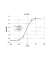
この(10)式をグラフ化すると、図9のようになる。
横軸に制御電圧Vcを−0.2Vから+0.2Vまでの範囲を0.1Vステップの目盛で示し、縦軸にGainを10dBステップの目盛で、0dBから−90dBの範囲を示している。また温度条件を27℃、−25℃、85℃と3つに設定した場合について、制御電圧Vcに対するそれぞれのGain特性を示してある。
制御電圧Vcが+0.2Vから+0.1Vの範囲では、温度条件に係わらず減衰量はほとんど0dBで、またVcが0.1Vから0Vの範囲でも減衰特性はほぼ同じで、0Vで約―6dBである。Vcが0V以下になると減衰量の温度依存性が出てくる。Vcが−0.1において、85℃で約―27dB、27℃で約−34dB、−25℃で約−41dBとなり、その差最大で10dB以上となり、温度に対するばらつきが大きくなることを示している。
また、Vcが−0.2Vになると、各減衰量は85℃で約―54dB、27℃で約−67dB、−25℃で約−82dBとなり、その差は最大で25dB以上となり、さらに温度に対するばらつきが大きいことを示している。
このように、図8に示したGCA回路250は良好な制御直線性及び温度特性とは言い難い。
FIG. 9 is a graph of this equation (10).
The horizontal axis indicates the range of the control voltage Vc from −0.2 V to +0.2 V in a scale of 0.1 V steps, and the vertical axis indicates the gain in a scale of 10 dB steps and a range of 0 dB to −90 dB. In addition, the gain characteristics with respect to the control voltage Vc are shown for the case where the temperature conditions are set to 27.degree. C., -25.degree. C., and 85.degree.
When the control voltage Vc is in the range of +0.2 V to +0.1 V, the attenuation is almost 0 dB regardless of the temperature condition, and the attenuation characteristic is almost the same even when the Vc is in the range of 0.1 V to 0 V, and about −6 dB at 0 V. It is. When Vc becomes 0 V or less, the temperature dependence of the attenuation amount appears. When Vc is −0.1, it is about −27 dB at 85 ° C., about −34 dB at 27 ° C., about −41 dB at −25 ° C., and the maximum difference is 10 dB or more. .
When Vc is -0.2 V, the attenuation is about -54 dB at 85 ° C, about -67 dB at 27 ° C, about -82 dB at -25 ° C, and the difference is 25 dB or more at the maximum. It shows that the variation is large.
Thus, the
また、図7、図8、図9における無線通信装置とGCA回路は、GCA回路を3段構成にしているため、消費電流が大きくなり、また3段構成とするため素子数が増えIC化する場合チップ面積が大きくなるなどの問題点がある。
以上述べたように、直交変調器MODと3段構成の利得制御増幅器(GCA回路)を設けた場合、GCA回路を3段構成にしているため、消費電流が大きくなり、またそれに伴って素子数が増えIC化する場合チップ面積が大きくなるなどの問題点がある。さらに、GCA回路を図8に示す回路構成にすると、制御直線性と温度特性に問題がある。
これらの問題を解決するために、本発明においては変調器と利得制御増幅器(GCA回路)の一部を組み合わせる回路構成とし、MODからの出力信号を電圧に変換する必要が無く電流でRF信号を授受することができようにする。それによって、MOD出力において、RF電流からRF電圧に変換するI−V変換回路や電圧レベルシフトを行うエミッタフォロアー回路などが不要になり、消費電流を削減できると共にチップ面積を縮小できるようにした。また、MODからGCA回路もレイアウトをし易くした。
RF信号を電流信号としてGCA回路に供給するようにしたので、配線容量の問題を回避でき、周波数特性も改善できる。
また、MODと組み合わせるGCA回路の回路構成とさらにその後段のGCA回路の新たな回路構成により、GCA回路の直線性と温度特性を向上させた。
As described above, when the quadrature modulator MOD and the three-stage gain control amplifier (GCA circuit) are provided, the GCA circuit has a three-stage structure, so that the current consumption increases, and the number of elements increases accordingly. When the IC is increased, the chip area becomes large. Furthermore, when the GCA circuit has the circuit configuration shown in FIG. 8, there is a problem in control linearity and temperature characteristics.
In order to solve these problems, the present invention adopts a circuit configuration in which a modulator and a part of a gain control amplifier (GCA circuit) are combined, and it is not necessary to convert an output signal from the MOD into a voltage, and an RF signal is generated by a current. Be able to give and receive. This eliminates the need for an IV conversion circuit that converts RF current to RF voltage and an emitter follower circuit that performs voltage level shift in the MOD output, thereby reducing current consumption and reducing the chip area. In addition, the MOD to GCA circuit is also easy to lay out.
Since the RF signal is supplied to the GCA circuit as a current signal, the wiring capacity problem can be avoided and the frequency characteristics can be improved.
Further, the linearity and temperature characteristics of the GCA circuit are improved by the circuit configuration of the GCA circuit combined with the MOD and the new circuit configuration of the GCA circuit at the subsequent stage.
本発明の通信装置は、送信に係る同相信号および直交位相信号を変調するために、差動の同相信号および差動の直交位相信号が入力されるベースバンド部、前記ベースバンド部から出力される差動のベースバンド信号とともに互いに逆相である差動の第1の発振信号および差動の第2の発振信号が入力される変調部、および、前記変調部から出力される差動のRF信号とともに利得制御用の差動の制御電圧が入力され、前記差動のRF信号を複数段の利得制御増幅回路により増幅する増幅部を有し、前記ベースバンド部は、第1の電流源が接続された第1の差動回路を有し、前記差動の同相信号を前記第1の差動回路により電流増幅し、前記第1の差動回路の一対の出力から差動電流による第1のベースバンド信号を出力する第1の増幅器と、第2の電流源が接続された第2の差動回路を有し、前記差動の直交位相信号を前記第2の差動回路により電流増幅し、前記第2の差動回路の一対の出力から差動電流による第2のベースバンド信号を出力する第2の増幅器とを有し、2対の差動電流である第1のベースバンド信号および第2のベースバンド信号を、前記変調部へ出力し、前記変調部は、前記差動電流による第1のベースバンド信号が各々に供給されるように前記第1の差動回路の一対の出力の各々に接続され、前記差動の第1の発振信号が互いに逆相に供給される2組の第3の差動回路を有し、前記2組の第3の差動回路による2組の差動の出力電流を合成して、位相が互いに異なる差動電流による第1の変調信号および第2の変調信号を出力する第1のギルバート型掛算器と、前記差動電流による第2のベースバンド信号が各々に供給されるように前記第2の差動回路の一対の出力の各々に接続され、前記差動の第1の発振信号と逆相の関係にある前記差動の第2の発振信号が互いに逆相に供給される2組の第4の差動回路を有し、前記2組の第3の差動回路による2組の差動の出力電流を合成して、位相が互いに異なる差動電流による第3の変調信号および第4の変調信号を出力する第2のギルバート型掛算器と、前記第1のギルバート型掛算器および前記第2のギルバート型掛算器に接続され、前記第1の発振信号の位相に対して正相の電流となる前記第1の変調信号と、前記第2の発振信号の位相に対して正相の電流となる前記第3の変調信号とを合成する第1の合成器と、前記第1のギルバート型掛算器および前記第2のギルバート型掛算器に接続され、前記第1の発振信号の位相に対して負相の電流となる前記第2の変調信号と、前記第2の発振信号の位相に対して負相の電流となる前記第4の変調信号とを合成する第2の合成器とを有し、前記第1の合成器および前記第2の合成器から前記増幅部へ、正相の電流および負相の電流による差動電流のRF信号を出力し、前記複数段の利得制御増幅回路のうちの初段の利得制御増幅回路は、前記正相の電流によるRF電流が供給されるように前記第1の合成器の出力に接続され、前記利得制御用の差動の制御電圧が供給される第5の差動回路と、前記第5の差動回路の差動出力のうちの一方の電流出力に接続される第1の負荷回路と、前記負相の電流によるRF電流が供給されるように前記第2の合成器の出力に接続され、前記利得制御用の差動の制御電圧が供給される第6の差動回路と、前記第6の差動回路の差動出力のうちの一方の電流出力に接続される第2の負荷回路とを有し、前記第1の負荷回路および前記第2の負荷回路は、前記利得制御用の差動の制御電圧に対して同じ側となるように前記第5の差動回路の前記一方の電流出力および前記第6の差動回路の前記一方の電流出力に接続され、前記差動電流のRF信号を前記差動の制御電圧に応じて増幅した差動の増幅信号を後段の利得制御増幅回路へ出力し、前記ベースバンド部の前記第1の増幅器と、前記変調部の前記第1のギルバート型掛算器および前記第1の合成器と、前記初段の利得制御増幅回路の前記第5の差動回路および前記第1の負荷回路とは、前記ベースバンド部の電流により動作するように、所定の電源電圧を示す第1の基準電位と、グランド電位を示す第2の基準電位との間にDC的に直列接続され、前記ベースバンド部の前記第2の増幅器と、前記変調部の前記第2のギルバート型掛算器および前記第2の合成器と、前記初段の利得制御増幅回路の前記第6の差動回路および前記第2の負荷回路とは、前記ベースバンド部の電流により動作するように、前記第1の基準電位と前記第2の基準電位との間にDC的に直列接続されている。
The communication apparatus according to the present invention outputs a baseband unit to which a differential in-phase signal and a differential quadrature signal are input in order to modulate an in-phase signal and a quadrature signal related to transmission. A differential baseband signal and a differential first oscillation signal and a differential second oscillation signal that are opposite in phase to each other, and a differential output from the modulation unit A differential control voltage for gain control is input together with the RF signal, and the differential RF signal is amplified by a plurality of stages of gain control amplifier circuits. The baseband unit includes a first current source. Are connected, and the differential common-mode signal is current- amplified by the first differential circuit, and a differential current is output from a pair of outputs of the first differential circuit. first amplifier that outputs a first baseband signal and A second differential circuit in which the second current source is connected, a quadrature phase signal of the differential current-amplified by the second differential circuit, a pair of outputs of said second differential circuit And a second amplifier that outputs a second baseband signal based on a differential current from the first baseband signal to the modulation unit. And the modulation unit is connected to each of a pair of outputs of the first differential circuit so that a first baseband signal based on the differential current is supplied to each of the first and second differential circuits . a third differential circuit 2 sets the oscillation signal is supplied to the opposite phases of synthesizes the output current of the two pairs of differential by the two pairs of the third differential circuit, phase first Gilbert type multiplier for outputting a first modulated signal and the No. 2 variant Choshin by different differential current When the second base band signal by the differential current is connected to each of the pair of outputs of said second differential circuit to be supplied to each, the first oscillation signal and the negative phase of the differential The differential second oscillation signals having the relationship of 2 are provided with two sets of fourth differential circuits to be supplied in opposite phases, and two sets of differentials by the two sets of third differential circuits the output current and synthesis of the second Gilbert type multiplier for outputting a third modulated signal and No. 4 variant Choshin by different phases differential current, the first Gilbert type multiplier and It is connected to the second Gilbert type multiplier, to the first and the first modulation signal as a current positive phase with respect to the phase of the oscillation signal, prior Symbol second oscillation signal of the phase a first combiner for combining the said third modulation signal as a positive phase current, the first Gilbert type multiplier And connected to said second Gilbert type multiplier, and the second modulation signal as a current negative-phase relative to the phase of the first oscillation signal, to the phase of the previous SL second oscillation signal Te and a second combiner for combining the said fourth modulated signal as a current negative-phase, from said first combiner and said second combiner to the amplifying unit, the positive phase An RF signal of a differential current based on a current and a negative phase current is output, and the first-stage gain control amplifier circuit of the plurality of gain control amplifier circuits is supplied with an RF current based on the positive phase current. connected to said first combiner output, and a fifth differential circuit control voltage of the differential for the gain control is supplied, one of the differential outputs of said fifth differential circuit wherein a first load circuit connected to the current output of, so that the RF current supplied by the current of the negative-phase first Is connected to the combiner output, and a sixth differential circuit for controlling voltage of the differential for the gain control is supplied, one of the current output of the differential output of the differential circuit of the sixth A second load circuit connected to the first load circuit , wherein the first load circuit and the second load circuit are on the same side with respect to the differential control voltage for gain control. 5. A differential that is connected to the one current output of the
本発明を用いることにより、利得制御増幅器を兼用し、利得制御増幅器の段数を削減できる。 By using this onset bright, also serves as a gain control amplifier, Ru can reduce the number of gain control amplifier.
図1に本発明の利得制御変調回路(器)を用いた通信装置10の送信ブロックのブロック構成を示す。図1に示す通信装置10は、BB(ベースバンド)ブロック、MODブロック、RFAGCブロックで構成されている。
BBブロックは、I(同相)信号、Q(直交位相)信号がそれぞれ供給される電圧増幅器、またはVI(電圧−電流)変換回路13,14で構成される。I,Q信号はこのBBブロックで電圧を増幅して、電圧を電流に変換した後MODブロックのミキサ15,16にベースバンド信号を出力する。
MODブロックは、本発明においては、上述のミキサ15,16、VCO(Voltage Contol Oscillator)21、Div(分周器)22、RF合成器17、さらにRFAGCの1段を構成する利得制御増幅器(GCA回路)18で構成されている。
BBブロックのVI変換回路13,14から出力された信号がミキサ15,16に供給される。一方このミキサ15,16にはVCO21からの発振信号がDiv22で分周され発振信号±LO_I,±LO_Qが供給される。そしてこのミキサ15,16の出力端子から出力されるRF信号は一般に電圧RF信号であるが、図1に示すようにミキサ15,16出力は電流出力とした。この電流(RF)信号は、RF合成器17でRF電流信号が合成されてGCA回路18に電流RF信号が出力される。
GCA回路18はMODブロックの一部に構成されていて、制御電圧(Vc)により利得が制御され、RF(電流)合成器17から供給された電流RF信号の振幅を制御された利得に応じて増幅し、後段のRFAGCブロックを構成するGCA回路(19)に出力する。
RFAGC(RF自動利得制御増幅器)ブロックは、従来は3段構成であったが、1段のGCA回路(18)はMODブロックに構成されているので、本発明においては2段構成(19,20)となっている。
FIG. 1 shows a block configuration of a transmission block of a
The BB block includes voltage amplifiers or VI (voltage-current)
In the present invention, the MOD block includes the above-described
Signals output from the
The
The RFAGC (RF automatic gain control amplifier) block conventionally has a three-stage configuration, but since the one-stage GCA circuit (18) is configured as a MOD block, the present invention has a two-stage configuration (19, 20). ).
このように、本発明におけるMODブロックは変調器と利得制御増幅器の一部を組み合わせる回路構成とし、またMODからの出力信号を電圧に変換する必要が無く電流でRF信号を授受することができようにした。それによって、MOD出力において、RF電流からRF電圧に変換するI−V変換回路や電圧レベルシフトを行うエミッタフォロアー回路などが不要になり、消費電流を削減できると共にチップ面積を縮小できるようにした。また、MODからGCA回路へのレイアウトをし易くした。
RF信号を電流信号としてGCA回路に供給するようにしたので、配線容量の問題を回避でき、周波数特性も改善できる。
また、MODと組み合わせるGCA回路の回路構成とさらにその後段のGCA回路の新たな回路構成により、GCA回路の直線性と温度特性を向上させることができる。
Thus, the MOD block according to the present invention has a circuit configuration in which a modulator and a part of a gain control amplifier are combined, and it is not necessary to convert an output signal from the MOD into a voltage, so that an RF signal can be exchanged with a current. I made it. This eliminates the need for an IV conversion circuit that converts RF current to RF voltage and an emitter follower circuit that performs voltage level shift in the MOD output, thereby reducing current consumption and reducing the chip area. In addition, the layout from the MOD to the GCA circuit is facilitated.
Since the RF signal is supplied to the GCA circuit as a current signal, the wiring capacity problem can be avoided and the frequency characteristics can be improved.
Further, the linearity and temperature characteristics of the GCA circuit can be improved by the circuit configuration of the GCA circuit combined with the MOD and the new circuit configuration of the GCA circuit at the subsequent stage.
つぎに図1に示した、通信装置の主要部の一部であるBBブロックとMODブロックの実施形態例を図2に示す。
図2に示すように、BBブロックはI信号を増幅する差動増幅器とQ信号を増幅する差動増幅器で構成されている。ここでは電圧増幅型の回路構成についてのべるが、これに限定されるべきでなく、電流増幅型の増幅器などでも良い。この実施形態例については後述する。
I信号を増幅する差動増幅器において、NPNトランジスタ51のエミッタとNPNトランジスタ52のエミッタが共通接続され、この共通接続点は定電流源I10を介してグランドに接続されている。NPNトランジスタ51とNPNトランジスタ52のベース間にVI(I)信号が供給され、各コレクタは一方のミキサの入力と接続されている。
また、Q信号を処理する回路も同様に、NPNトランジスタ53のエミッタとNPNトランジスタ54のエミッタが共通接続され、この共通接続点は定電流源I11を介してグランドに接続されている。NPNトランジスタ53とNPNトランジスタ54のベース間にVQ(Q)信号が供給され、各コレクタは他方のミキサの入力と接続されている。
Next, FIG. 2 shows an embodiment of the BB block and the MOD block which are a part of the main part of the communication apparatus shown in FIG.
As shown in FIG. 2, the BB block includes a differential amplifier that amplifies the I signal and a differential amplifier that amplifies the Q signal. Here, a voltage amplification type circuit configuration will be described, but it should not be limited to this, and a current amplification type amplifier or the like may be used. This embodiment will be described later.
In the differential amplifier that amplifies the I signal, the emitter of the
Similarly, in the circuit for processing the Q signal, the emitter of the
つぎにMODブロックについて述べる。このMODブロックは主にギルバート型掛算器で構成されていている。具体的には、I信号を変調するミキサとQ信号を変調するミキサ、さらにこのミキサ出力の電流RF信号を合成するRF合成器17とGCA回路18とで構成されている。
具体的には、I信号を変調するミキサにおいて、NPNトランジスタ55のエミッタはNPNトランジスタ56のエミッタと共通接続され、この共通接続点が上述したBBブロックの差動増幅器を構成するNPNトランジスタ51のコレクタに接続される。またNPNトランジスタ57のエミッタはNPNトランジスタ58のエミッタと共通接続され、この共通接続点が上述したBBブロックの差動増幅器を構成するNPNトランジスタ52のコレクタに接続される。NPNトランジスタ55のベースはNPNトランジスタ58のベースに接続され発振信号+LO_Iが供給され、NPNトランジスタ56のベースはNPNトランジスタ57のベースに接続され発振信号−LO_Iが供給される。
Q信号を変調するミキサにおいて、NPNトランジスタ59のエミッタはNPNトランジスタ60のエミッタと共通接続され、この共通接続点が上述したBBブロックの差動増幅器を構成するNPNトランジスタ53のコレクタに接続される。またNPNトランジスタ61のエミッタはNPNトランジスタ62のエミッタと共通接続され、この共通接続点が上述したBBブロックの差動増幅器を構成するNPNトランジスタ54のコレクタに接続される。NPNトランジスタ59ベースはNPNトランジスタ62のベースに接続され発振信号+LO_Qが供給され、NPNトランジスタ60のベースはNPNトランジスタ61のベースに接続され発振信号−LO_Qが供給される。
NPNトランジスタ55のコレクタとNPNトランジスタ57のコレクタが接続され+Imix_Iの信号を出力する。NPNトランジスタ56のコレクタとNPNトランジスタ58のコレクタが接続され−Imix_Iの信号を出力する。同様に、NPNトランジスタ59のコレクタとNPNトランジスタ61のコレクタが接続され+Imix_Qの信号を出力する。NPNトランジスタ60のコレクタとNPNトランジスタ62のコレクタが接続され−Imix_Qの信号を出力する。
Next, the MOD block will be described. This MOD block is mainly composed of a Gilbert type multiplier. More specifically, it comprises a mixer that modulates the I signal, a mixer that modulates the Q signal, an
Specifically, in the mixer that modulates the I signal, the emitter of the
In the mixer for modulating the Q signal, the emitter of the
The collector of the
つぎにRF合成器17に相当する回路構成について述べる。それぞれのミキサはオープンコレクタの回路構成となっているので、各コレクタを接続することにより構成することができる。
NPNトランジスタ55とNPNトランジスタ57のコレクタ共通接続点とNPNトランジスタ59とNPNトランジスタ61のコレクタ共通接続点が接続され、+Imix_Iと+Imix_Qと電流合成され、+Imodの変調されたRF電流が出力される。
また、NPNトランジスタ56とNPNトランジスタ58のコレクタ共通接続点とNPNトランジスタ60とNPNトランジスタ62のコレクタ共通接続点が接続され、−Imix_Iと−Imix_Qが電流合成され、−Imodの変調されたRF電流が出力される。
Next described circuit configuration corresponding to the
A collector common connection point of the
In addition, the collector common connection point of the
つぎにRF合成器17のRF信号レベルを制御電圧により制御するGCA回路18について述べる。このGCA回路18は、MODブロックの一部として構成されているところに特徴があり、たとえば差動型増幅器で構成されている。
RF合成器17の出力である、+ImodがNPNトランジスタ65とNPNトランジスタ66の共通エミッタに接続され、NPNトランジスタ65コレクタは負荷Z1(71)を介して電源Vccに接続され、このコレクタから出力電圧が取り出される。またNPNトランジスタ66のコレクタは直接電源Vccに接続される。
−ImodがNPNトランジスタ67とNPNトランジスタ68の共通エミッタに接続され、NPNトランジスタ68コレクタは負荷Z1(72)を介して電源Vccに接続され、このコレクタから出力電圧が取り出される。またNPNトランジスタ67のコレクタは直接電源Vccに接続される。
NPNトランジスタ65のベースとNPNトランジスタ68のベースが共通接続され、制御電圧+Vcが供給される。また、NPNトランジスタ66のベースとNPNトランジスタ67のベースが共通接続され、制御電圧−Vcが供給される。
Next, the
Which is the output of the
-Imod is connected to the common emitter of
The base of the
図2に示すBBブロックとMODブロックの動作について述べる。BBブロックのNPNトランジスタ51,52の両ベース間にVI(I)信号が供給され、増幅されてそれぞれのコレクタから+I_BBIと−I_BBIの電流信号が出力される。+I_BBI信号はミキサを構成するNPNトランジスタ55,56の共通エミッタに供給される。−I_BBI信号はミキサを構成するNPNトランジスタ57,58の共通エミッタに供給され、NPNトランジスタ55,58のベースには発振信号+LO_IがNPNトランジスタ56,57のベースには−LO_Iがそれぞれ供給される。NPNトランジスタ55とNPNトランジスタ57のコレクタ出力を加算して変調信号+Imix_Iを出力する。また同様に、NPNトランジスタ56とNPNトランジスタ58のコレクタ出力を加算して変調信号−Imix_Iを出力する。
Q信号の変調についても同様に、BBブロックのNPNトランジスタ53,54の両ベース間にVQ(Q)信号が供給され、増幅されてそれぞれのコレクタから+I_BBQと−I_BBQの電流信号が出力される。+I_BBQ信号はミキサを構成するNPNトランジスタ59,60の共通エミッタに供給される。−I_BBQ信号はミキサを構成するNPNトランジスタ61,62の共通エミッタに供給され、NPNトランジスタ59,62のベースには発振信号+LO_Qが、またNPNトランジスタ60,61のベースには−LO_Qがそれぞれ供給される。NPNトランジスタ59とNPNトランジスタ61のコレクタ出力を加算して変調信号+Imix_Qを出力する。また同様に、NPNトランジスタ60とNPNトランジスタ62のコレクタ出力を加算して変調信号−Imix_Qを出力する。
The operation of the BB block and the MOD block shown in FIG. 2 will be described. A VI (I) signal is supplied between both bases of the
Similarly for the modulation of the Q signal, the VQ (Q) signal is supplied between the bases of the
変調信号+Imix_Iと+Imix_Qが加算されて+ImodのRF変調信号が得られる。また変調信号−Imix_Iと−Imix_Qが加算されて−ImodのRF変調信号が得られる。そして、ミキサで得られたそれぞれの変調信号+Imod、−ImodをGCA回路18に供給する。
GCA回路18において、制御電圧Vc(,−Vc)を可変して利得を可変して、NPNトランジスタ65のコレクタ、NPNトランジスタ68のコレクタからRF信号を取り出す。このGCA回路については、図8に示した回路構成とその特性も同じである。
しかし、このGCA回路18については後述する(図3,5に示す)ように、他の実施形態例の回路構成であってもよく、これらの回路構成に限定されるべきものではない。
The modulation signals + Imix_I and + Imix_Q are added to obtain a + Imod RF modulation signal. Further, the modulation signals -Imix_I and -Imix_Q are added to obtain an RF modulation signal of -Imod. Then, each modulation signal + Imod, −Imod obtained by the mixer is supplied to the
In the
However, as will be described later (shown in FIGS. 3 and 5), the
上述したように、変調器(回路)とこれを用いた通信装置はGCA回路をMODの一部に組み合わせたことにより、MOD出力信号を電圧に変換する必要が無く電流でRF信号を授受することができる。それによって、MOD出力において、RF電流からRF電圧に変換するI−V変換回路や電圧レベルシフトを行うエミッタフォロアー回路などが不要になり、消費電流を削減できると共にチップ面積を縮小できるようにした。また、MODからGCA回路もレイアウトをし易くした。
RFを電流信号としてGCA回路に供給するようにしたので、配線容量の問題を回避でき、周波数特性も改善できる。
As described above, a modulator (circuit) and a communication device using the modulator can exchange an MOD output signal into a voltage without transmitting a MOD output signal by combining a GCA circuit with a part of the MOD, and can exchange an RF signal with a current. Can do. This eliminates the need for an IV conversion circuit that converts RF current to RF voltage and an emitter follower circuit that performs voltage level shift in the MOD output, thereby reducing current consumption and reducing the chip area. In addition, the MOD to GCA circuit is also easy to lay out.
Since RF is supplied to the GCA circuit as a current signal, the problem of wiring capacity can be avoided and the frequency characteristics can be improved.
図2の通信装置50において、BBブロック70はバイポーラトランジスタを用いた2個の差動増幅器で構成した。BBブロックに用いるベースバンド信号を処理する回路はこれ以外に、後述する図4に示すたとえばMOSトランジスタなどで構成したVI変換回路を用いて構成することもできるが、本発明はこれらの回路に限定されるべきものではない。
In the
つぎに、他の実施形態例であるBBブロック部とMODブロックを有する通信装置90の構成について図3を用いて述べる。
図3において、BBブロックを構成する回路構成とMODブロックの一部を構成するGCA回路の回路構成が図2の対応ブロックと異なっている。しかし、MODブロックを構成するミキサの回路構成は図2に示した回路構成と同じであり、またMOD全体の動作は図2と基本的に同じであるので詳細な説明は省略し、各ブロックの動作について説明する。
Next, the configuration of a
In FIG. 3, the circuit configuration of the BB block and the circuit configuration of the GCA circuit forming a part of the MOD block are different from the corresponding blocks in FIG. However, the circuit configuration of the mixer constituting the MOD block is the same as the circuit configuration shown in FIG. 2, and the overall operation of the MOD is basically the same as FIG. The operation will be described.
図3において、BBブロック回路110はVI変換回路120A,120Bの2個のVI変換回路で構成されていて、その実施形態例の回路構成であるVI変換回路120を図4に示す。
図4に示すように、PMOSトランジスタ125とPMOSトランジスタ126で差動増幅器を構成し、出力信号はカレントミラー回路を用いて電流出力とする構成となっている。
+Vinの信号経路において、電源Vccに定電流源I120の一方の端子が接続され、他方の端子はPMOSトランジスタ125のソースと、オペアンプ127の反転入力端子と抵抗129の一方の端子とに接続されている。オペアンプ127の非反転入力端子に入力信号Vinが供給される。出力はPMOSトランジスタ125のゲートに接続されている。このPMOSトランジスタ125のドレインはソース接地のNMOSトランジスタ121のドレインとゲートに接続される。またNMOSトランジスタ121のゲートはカレントミラーを構成するソース接地型のNMOSトランジスタ122のゲートに接続され、このNMOSトランジスタ122のドレインから出力信号が電流として出力される。
ここで、カレントミラーを構成するNMOSトランジスタ121とNMOSトランジスタ122の面積比(ゲート幅の比)は1:mと設定し、NMOSトランジスタ121に流れる電流のm倍の電流をNMOSトランジスタ122のドレインから出力するようにしている。
一方、−Vinの信号経路において、電源Vccに定電流源I121の一方の端子が接続され、他方の端子はPMOSトランジスタ126のソースと、オペアンプ128の反転入力端子と抵抗129の他方の端子とに接続されている。オペアンプ128の非反転入力端子に入力信号−Vinが供給される。出力はPMOSトランジスタ126のゲートに接続されている。このPMOSトランジスタ126のドレインはソース接地のNMOSトランジスタ123のドレインとゲートに接続される。またNMOSトランジスタ123のゲートはカレントミラーを構成するソース接地NMOSトランジスタ124のゲートに接続され、このNMOSトランジスタ124のドレインから出力信号が電流として出力される。
ここで、カレントミラーを構成するNMOSトランジスタ123とNMOSトランジスタ124の面積比(ゲート幅の比)は1:mと設定し、NMOSトランジスタ123に流れる電流のm倍の電流をNMOSトランジスタ124のドレインから出力するようにしている。
In FIG. 3, the
As shown in FIG. 4, a
In the + Vin signal path, one terminal of the constant current source I120 is connected to the power supply Vcc, and the other terminal is connected to the source of the
Here, the area ratio (gate width ratio) of the
On the other hand, in the signal path of −Vin, one terminal of the constant current source I121 is connected to the power supply Vcc, and the other terminal is connected to the source of the
Here, the area ratio (gate width ratio) of the
つぎに、このVI変換回路120の動作について述べる。
入力信号Vinがオペアンプ127の入力で端子Aの電圧と比較され、その差電圧が差動増幅器を構成するPMOSトランジスタ125のゲートに供給され、電流を増減してソース電圧の端子AがVinに等しくなるように帰還がかかる。同様に−Vinがオペアンプ128の入力で端子Bの電圧と比較され、その差電圧がPMOSトランジスタ126のゲートに供給され、電流を増減して端子Bの電圧が−Vinに等しくなるように帰還がかかる。そして、入力電圧(Vin,−Vin)がレベルシフトされて増幅器の端子A,Bにそれぞれ出力される。
その結果、端子Aと端子B間に発生した電圧差を抵抗129で電流に変換する。この電流即ち信号電流(交流)が図4に示すようにPMOSトランジスタ126、NMOSトランジスタ123、NMOSトランジスタ121、PMOSトランジスタ125さらに抵抗129と流れる。
NMOSトランジスタ121とNMOSトランジスタ122はカレントミラー回路を構成しているので、NMOSトランジスタ121に流れる電流をm倍した電流がNMOSトランジスタ122のドレインから信号電流が流れる。また同様に、NMOSトランジスタ123に流れる電流をm倍した電流がNMOSトランジスタ124のドレインから信号電流が流れる。
Next, the operation of the
The input signal Vin is compared with the voltage of the terminal A at the input of the
As a result, the voltage difference generated between the terminal A and the terminal B is converted into a current by the
Since the
図4に示した入力信号Vinが図3に示したBBブロックの入力信号VI信号のとき、VI変換回路120をVI変換回路120Aとし、入力信号VinがVQ信号のとき、VI変換回路120をVI変換回路120Bとする。
図3のVI変換回路120Aにおいて、Vin(VI)信号が入力され、その結果NMOSトランジスタ122のドレインから出力された信号電流(−I_BBI)はミキサを構成するNPNトランジスタ97,98の共通エミッタに供給される。またNMOSトランジスタ124のドレインから出力される信号電流(+I_BBI)はミキサを構成するNPNトランジスタ95,96の共通エミッタに供給される。
またVI変換器120Bにおいても同様に、入力信号Vin(VQ)が供給されると、カレントミラーを構成するNMOSトランジスタの各ドレインから出力される信号電流はミキサを構成するNPNトランジスタ101,102、NPNトランジスタ99,100の共通エミッタにそれぞれ供給される。
When the input signal Vin shown in FIG. 4 is the input signal VI signal of the BB block shown in FIG. 3, the
In the
Similarly, in the
図4に示すVI変換回路120において、出力トランジスタ、NMOSトランジスタ122,124の各ドレインは直接ミキサを構成するNPNトランジスタ99,100、NPNトランジスタ101,102の共通エミッタに接続されている。BBブロック、ミキサ、利得制御増幅器(GCA回路)を電源Vccとグランド間に接続するとき、VI変換回路120にはNMOSトランジスタ122,124のVDS(ドレイン−ソース間)電圧だけ必要でその電圧は小さくでき、それ以外の電圧(Vcc−VDS)はミキサと利得制御増幅器(GCA回路)で設定することができ、設計マージンが多くなり、またそれに伴って、ミキサまたは利得制御増幅器(GCA回路)の動作電圧を大きくすることができるので、線形性領域が広くなる利点がある。
In the
つぎに、ミキサの動作については図2に示した通信装置90のミキサと同じであるのでここでは数式を用いて概略を説明し、詳細な説明は省略する。
BBブロックからの出力電流をそれぞれ+I_BBI,−I_BBI,+I_BBQ,−I_BBQとする。
信号成分; I_BBI=cosωb、I_BBQ=sinωb
LO成分; I_LOI=cosωlo、I_LOQ=sinωlo
と設定すると、MIX動作により生成される電流Imix_I,Imix_Qはそれぞれ
Imix_I=cosωlo*cosωb ・・・(11)
Imix_Q=−sinωlo*sinωb ・・・(12)
となる。この式(11)、(12)より、ミキサ出力電流Imodは、
Imod=(Imix_I)+(Imix_Q)
=cos(ωlo+ωb) ・・・(13)
となり、イメージ信号成分(cos(ωlo-ωb))は除去される。このイメージ成分が除去された変調波(信号)がミキサ出力にカスコード接続されたGCA回路(18)に供給される。
Next, since the operation of the mixer is the same as that of the mixer of the
Output currents from the BB block are + I_BBI, -I_BBI, + I_BBQ, and -I_BBQ, respectively.
Signal component; I_BBI = cosωb, I_BBQ = sinωb
LO component; I_LOI = cosωlo, I_LOQ = sinωlo
Is set, the currents Imix_I and Imix_Q generated by the MIX operation are respectively
Imix_I = cosωlo * cosωb (11)
Imix_Q = −sinωlo * sinωb (12)
It becomes. From these equations (11) and (12), the mixer output current Imod is
Imod = (Imix_I) + (Imix_Q)
= Cos (ωlo + ωb) (13)
Thus, the image signal component (cos (ωlo−ωb)) is removed. The modulated wave (signal) from which the image component has been removed is supplied to a GCA circuit (18) cascode-connected to the mixer output.
つぎに、図3において、RF(電流)合成器17から出力されたRF信号のレベルを制
御電圧(+Vc,−Vc)で利得を制御する他の実施形態例のGCA回路(18)の構成について述べる。このGCA回路(18)は、MODブロックの一部として構成されているところに特徴があり、差動型増幅器で構成され、図2のGCA回路(18)とは負荷回路の構成が異なる。
RF合成器17の出力から+ImodがNPNトランジスタ105とNPNトランジスタ106の共通エミッタに供給される。NPNトランジスタ105のコレクタはキャパシタC1とインダクタL1が並列接続された負荷Z1を介して電源Vccに接続されまた抵抗R2の一方の端子に接続されている。またこのコレクタから出力電圧が取り出される。
NPNトランジスタ106のコレクタは抵抗R1を介して電源Vccに接続されると共に、抵抗R2の他方の端子に接続される。
同様に、−ImodがNPNトランジスタ107とNPNトランジスタ108の共通エミッタに供給される。NPNトランジスタ108のコレクタはキャパシタC1AとインダクタL1Aが並列接続された負荷Z1Aを介して電源Vccに接続されまた抵抗R2Aの一方の端子に接続されている。またこのコレクタから出力電圧が取り出される。
NPNトランジスタ107のコレクタは抵抗R1Aを介して電源Vccに接続されると共に、抵抗R2Aの他方の端子に接続される。
Z1とZ1Aの回路はキャパシタC1とインダクタL1またはキャパシタC1AとインダクタL1Aとでそれぞれ構成されているが、これは並列共振回路を構成して、所望の周波数たとえば800MHzまたは2GHzの周波数で並列共振して、キャリアを取り出すバンドパスフィルタとしての働きをし、これらのキャリアを出力端子から取り出している。
Next, in FIG. 3, the configuration of the GCA circuit (18) of another embodiment in which the gain of the level of the RF signal output from the RF (current)
From the output of the
The collector of the
Similarly, −Imod is supplied to the common emitter of the
The collector of the
The circuits of Z1 and Z1A are composed of a capacitor C1 and an inductor L1 or a capacitor C1A and an inductor L1A, respectively, which form a parallel resonance circuit and perform parallel resonance at a desired frequency, for example, 800 MHz or 2 GHz. It functions as a band-pass filter for extracting carriers, and these carriers are extracted from the output terminal.
このGCA回路(18)の動作について、図5を用いて具体的に説明する。図5においてまず回路構成に付いて述べる。ミキサから出力される信号電流Iobの出力端子がNPNトランジスタ151とNPNトランジスタ152の共通エミッタに接続され、NPNトランジスタ151のコレクタは負荷Z1B(154)を介して電源Vccに接続されまた抵抗R2B(153)の一方の端子に接続されている。またこのコレクタから出力電圧が取り出される。
NPNトランジスタ152のコレクタは抵抗R1B(155)を介して電源Vccに接続されると共に、抵抗R2B(153)の他方の端子に接続される。即ち、差動回路の出力回路がパイ(Π)型構成になっていて、差動出力を合成している。
つぎにこのGCA回路150の回路動作を以下に示す。信号電流がNPNトランジスタ151,152の共通エミッタから入力され、制御電圧Vcを可変することによりこの信号電流の減衰量が変わる。この回路においては、負荷回路がZ1B,R2B,R1Bで構成され、NPNトランジスタ151のコレクタから出力(信号)Voが導出される。
出力Voは次式で表せる。
Vo=〔Z1B//(R1B+R2B)〕×I1B+〔(Z1B+R2B)//R1B×Z1B/(Z1B+R2B)〕×I2B
=Rmax×Iob/[1+exp(-Vc/Vt)]+Rmin×Iob/[1+exp(Vc/Vt)] ・・・(14)
但し、Rmax=Z1B×(R1B+R2B)/(R1B+R2B+Z1B) , Rmin=Z1B×R1B/(R1B+R2B+Z1B)
Vc=VBE1-VBE2 , Vt:ボルツマン定数
この回路の特性を分かり易くするため、仮に入力電圧Vi=1、Z1B=R1B=R2B=IoB=1と置くと、
利得Gain=(2/3)/ [1+exp(-Vc/Vt)]+(1/3)/[1+exp(Vc/Vt)] ・・・(15)
となる。
The operation of the GCA circuit (18) will be specifically described with reference to FIG. In FIG. 5, the circuit configuration will be described first. The output terminal of the signal current Iob output from the mixer is connected to the common emitter of the
The collector of the
Next, the circuit operation of the
The output Vo can be expressed by the following equation.
Vo = [Z1B // (R1B + R2B)] × I1B + [(Z1B + R2B) // R1B × Z1B / (Z1B + R2B)] × I2B
= Rmax × Iob / [1 + exp (−Vc / Vt)] + Rmin × Iob / [1 + exp (Vc / Vt)] (14)
However, Rmax = Z1B × (R1B + R2B) / (R1B + R2B + Z1B), Rmin = Z1B × R1B / (R1B + R2B + Z1B)
Vc = VBE1-VBE2, Vt: Boltzmann constant
To make the characteristics of this circuit easier to understand, if the input voltage Vi = 1, Z1B = R1B = R2B = IoB = 1,
Gain Gain = (2/3) / [1 + exp (−Vc / Vt)] + (1/3) / [1 + exp (Vc / Vt)] (15)
It becomes.
この(15)式をグラフ化すると、図6のようになる。横軸には制御電圧Vcを示し、0.1Vステップで−0.2Vから+0.2Vの範囲を示している。また縦軸にはGain(利得)を示し、1dBステップで−3dBから−10dBの範囲を示している。
温度条件は−25℃,27℃,85℃のとし、制御電圧Vcを可変したときのGainを示した。図6から、利得制御範囲が、最大利得と、最小利得によって制限されて有限な幅に制御される。そして、その制御特性は中利得、この例においては−6dBに関してほぼ点対称になり、さらに温度―25℃〜+85℃の範囲における特性のばらつきは非常に小さい。実際には、この利得制御変調回路(器)の後段に利得制御増幅器を2段置き、これらをオーバーラップさせ、温度特性を相殺し、良好な直線性及び、温度特性を持つ。なお、本発明はCDMA方式における利得制御変調回路(器)として説明したが、この通信方式に限定されるものではなく、本発明を応用できる他の方式にも有効である。
This equation (15) is graphed as shown in FIG. The horizontal axis shows the control voltage Vc, and shows a range from -0.2V to + 0.2V in 0.1V steps. The vertical axis indicates Gain (gain), and the range from -3 dB to -10 dB in 1 dB steps.
The temperature conditions are −25 ° C., 27 ° C., and 85 ° C., and Gain is shown when the control voltage Vc is varied. From FIG. 6, the gain control range is limited to the maximum gain and the minimum gain, and is controlled to a finite width. The control characteristic is substantially point-symmetric with respect to the medium gain, in this example -6 dB, and the characteristic variation in the temperature range of -25 ° C to + 85 ° C is very small. Actually, two gain control amplifiers are placed in the subsequent stage of the gain control modulation circuit (unit), they are overlapped, the temperature characteristics are canceled out, and the linearity and temperature characteristics are good. Although the present invention has been described as a gain control modulation circuit (unit) in the CDMA system, the present invention is not limited to this communication system, and is effective for other systems to which the present invention can be applied.
上述したように、通信装置の送信系の変調回路について説明したが、これに限定されるべきものでなく、本発明は通信装置の受信系の復調回路、たとえばミキサ回路とその周辺回路にも適用できることは明らかである。 As described above, the transmission system modulation circuit of the communication apparatus has been described. However, the present invention should not be limited to this, and the present invention is also applicable to the reception system demodulation circuit of the communication apparatus, such as a mixer circuit and its peripheral circuits. Obviously we can do it.
このように、変調器(回路)と利得制御増幅器の一部を組み合わせる回路構成とし変調(復調)器(回路)出力に独立して従来3段構成にされていたGCA回路を2段の回路構成とし、消費電流を削減できるようにした。またMOD出力信号を電圧に変換する必要が無く電流でRF信号を授受することができようにしたことにより、MODからGCA回路へのレイアウトをし易くした。さらにMOD出力信号を電流出力としてGCA回路に供給するようにしたので、配線容量の問題を回避でき、周波数特性も改善できる。
MOD出力において、RF電流からRF電圧に変換するI−V変換回路や電圧レベルシフトを行うエミッタフォロアー回路などが不要になり、消費電流を削減できると共にチップ面積を縮小できるようにした。
また、MODと組み合わせるGCA回路の回路構成とさらにその後段のGCA回路の新たな回路構成により、GCA回路の直線性と温度特性を向上させた。
In this way, a circuit configuration in which a modulator (circuit) and a part of the gain control amplifier are combined is used, and the GCA circuit that has been conventionally configured in three stages independently of the modulator (demodulator) output (circuit) is configured in two stages. The current consumption can be reduced. Further, since it is not necessary to convert the MOD output signal into a voltage and the RF signal can be exchanged with a current, the layout from the MOD to the GCA circuit is facilitated. Furthermore, since the MOD output signal is supplied to the GCA circuit as a current output, the problem of wiring capacitance can be avoided and the frequency characteristics can be improved.
In the MOD output, an IV conversion circuit for converting an RF current into an RF voltage and an emitter follower circuit for performing a voltage level shift become unnecessary, so that current consumption can be reduced and a chip area can be reduced.
Further, the linearity and temperature characteristics of the GCA circuit are improved by the circuit configuration of the GCA circuit combined with the MOD and the new circuit configuration of the GCA circuit at the subsequent stage.
10,200…通信装置、13,14,120,120A,120B…VI変換回路、15,16,202…ミキサ、18,19,20,203A,203B,203C…GCA回路(利得制御増幅器)、21…VCO(電圧制御型発振器)、22…Div(分周器)、51〜68,95〜108,151,152…NPNバイポーラトランジスタ、71,72,154…負荷(インピーダンス)、50,90…利得制御変調回路(器)、121〜124…NMOSトランジスタ、125,126…PMOSトランジスタ、127,128…オペアンプ、129,153,155…抵抗、201…変調器、205…SAW(ソーフィルタ)、206…パワーアンプ(PA)、208…DUP(ディユープレックサ)、208…ANT(アンテナ)。
DESCRIPTION OF SYMBOLS 10,200 ... Communication apparatus, 13, 14, 120, 120A, 120B ... VI conversion circuit, 15, 16, 202 ... Mixer, 18, 19, 20, 203A, 203B, 203C ... GCA circuit (gain control amplifier), 21 ... VCO (voltage controlled oscillator), 22 ... Div (divider), 51-68, 95-108, 151,152 ... NPN bipolar transistor, 71,72,154 ... Load (impedance), 50,90 ... Gain Control modulation circuit (unit), 121-124 ... NMOS transistor, 125, 126 ... PMOS transistor, 127, 128 ... operational amplifier, 129, 153, 155 ... resistance, 201 ... modulator, 205 ... SAW (saw filter), 206 ... Power amplifier (PA), 208 ... DUP (Duplexer), 208 ... ANT (ante) ).
Claims (2)
前記ベースバンド部は、
第1の電流源が接続された第1の差動回路を有し、前記差動の同相信号を前記第1の差動回路により電流増幅し、前記第1の差動回路の一対の出力から差動電流による第1のベースバンド信号を出力する第1の増幅器と、
第2の電流源が接続された第2の差動回路を有し、前記差動の直交位相信号を前記第2の差動回路により電流増幅し、前記第2の差動回路の一対の出力から差動電流による第2のベースバンド信号を出力する第2の増幅器と
を有し、2対の差動電流である第1のベースバンド信号および第2のベースバンド信号を、前記変調部へ出力し、
前記変調部は、
前記差動電流による第1のベースバンド信号が各々に供給されるように前記第1の差動回路の一対の出力の各々に接続され、前記差動の第1の発振信号が互いに逆相に供給される2組の第3の差動回路を有し、前記2組の第3の差動回路による2組の差動の出力電流を合成して、位相が互いに異なる差動電流による第1の変調信号および第2の変調信号を出力する第1のギルバート型掛算器と、
前記差動電流による第2のベースバンド信号が各々に供給されるように前記第2の差動回路の一対の出力の各々に接続され、前記差動の第1の発振信号と逆相の関係にある前記差動の第2の発振信号が互いに逆相に供給される2組の第4の差動回路を有し、前記2組の第3の差動回路による2組の差動の出力電流を合成して、位相が互いに異なる差動電流による第3の変調信号および第4の変調信号を出力する第2のギルバート型掛算器と、
前記第1のギルバート型掛算器および前記第2のギルバート型掛算器に接続され、前記第1の発振信号の位相に対して正相の電流となる前記第1の変調信号と、前記第2の発振信号の位相に対して正相の電流となる前記第3の変調信号とを合成する第1の合成器と、
前記第1のギルバート型掛算器および前記第2のギルバート型掛算器に接続され、前記第1の発振信号の位相に対して負相の電流となる前記第2の変調信号と、前記第2の発振信号の位相に対して負相の電流となる前記第4の変調信号とを合成する第2の合成器と
を有し、前記第1の合成器および前記第2の合成器から前記増幅部へ、正相の電流および負相の電流による差動電流のRF信号を出力し、
前記複数段の利得制御増幅回路のうちの初段の利得制御増幅回路は、
前記正相の電流によるRF電流が供給されるように前記第1の合成器の出力に接続され、前記利得制御用の差動の制御電圧が供給される第5の差動回路と、
前記第5の差動回路の差動出力のうちの一方の電流出力に接続される第1の負荷回路と、
前記負相の電流によるRF電流が供給されるように前記第2の合成器の出力に接続され、前記利得制御用の差動の制御電圧が供給される第6の差動回路と、
前記第6の差動回路の差動出力のうちの一方の電流出力に接続される第2の負荷回路と
を有し、
前記第1の負荷回路および前記第2の負荷回路は、
前記利得制御用の差動の制御電圧に対して同じ側となるように前記第5の差動回路の前記一方の電流出力および前記第6の差動回路の前記一方の電流出力に接続され、前記差動電流のRF信号を前記差動の制御電圧に応じて増幅した差動の増幅信号を後段の利得制御増幅回路へ出力し、
前記ベースバンド部の前記第1の増幅器と、前記変調部の前記第1のギルバート型掛算器および前記第1の合成器と、前記初段の利得制御増幅回路の前記第5の差動回路および前記第1の負荷回路とは、前記ベースバンド部の電流により動作するように、所定の電源電圧を示す第1の基準電位と、グランド電位を示す第2の基準電位との間にDC的に直列接続され、
前記ベースバンド部の前記第2の増幅器と、前記変調部の前記第2のギルバート型掛算器および前記第2の合成器と、前記初段の利得制御増幅回路の前記第6の差動回路および前記第2の負荷回路とは、前記ベースバンド部の電流により動作するように、前記第1の基準電位と前記第2の基準電位との間にDC的に直列接続されている
通信装置。 In order to modulate the in-phase signal and the quadrature signal for transmission, a baseband unit to which a differential in-phase signal and a differential quadrature signal are input, and a differential baseband output from the baseband unit A modulation unit that receives a differential first oscillation signal and a differential second oscillation signal that are opposite to each other together with a signal, and a differential RF signal that is output from the modulation unit. A differential control voltage is input, and the differential RF signal is amplified by a plurality of stages of gain control amplification circuits.
The baseband part is
A first differential circuit to which a first current source is connected; the differential common-mode signal is current- amplified by the first differential circuit; and a pair of outputs of the first differential circuit is used. A first amplifier for outputting a first baseband signal based on a differential current ;
A second differential circuit to which a second current source is connected; the differential quadrature signal is current amplified by the second differential circuit; and a pair of outputs of the second differential circuit A second amplifier for outputting a second baseband signal based on a differential current from
A first baseband signal and a second baseband signal, which are two pairs of differential currents, are output to the modulation unit;
The modulator is
The first baseband signal based on the differential current is connected to each of a pair of outputs of the first differential circuit so that the first baseband signal is supplied to each, and the differential first oscillation signals are out of phase with each other. The first differential circuit includes first and second differential currents that are different in phase from each other by synthesizing two sets of differential output currents from the two third differential circuits . a first Gilbert type multiplier for outputting a modulated signal and the No. 2 variant Choshin,
A second baseband signal based on the differential current is connected to each of a pair of outputs of the second differential circuit so as to be supplied to each, and has a phase relationship opposite to that of the differential first oscillation signal. has two sets of a fourth differential circuit second oscillation signal of the differential is supplied to the opposite phase in the two pairs of third outputs of two sets of differential by the differential circuit by combining the current, and a second Gilbert type multiplier for outputting a third modulated signal and No. 4 variant Choshin by different phases differential current,
Connected to said first Gilbert type multiplier and the second Gilbert type multiplier, and the first modulation signal as a current of positive-phase relative to the phase of the first oscillation signal, prior Symbol first a first combiner for combining the said third modulation signal as a current of positive phase with respect to the second oscillation signal phase,
Connected to said first Gilbert type multiplier and the second Gilbert type multiplier, and the second modulation signal as a current negative-phase relative to the phase of the first oscillation signal, prior Symbol first a second combiner for combining the said fourth modulated signal as a current negative-phase relative to the phase of the second oscillation signal
And outputting an RF signal of a differential current based on a positive phase current and a negative phase current from the first synthesizer and the second synthesizer to the amplification unit,
The first stage gain control amplifier circuit of the plurality of stages of gain control amplifier circuits is:
A fifth differential circuit connected to the output of the first combiner so that RF current is supplied, the control voltage of the differential for the gain control is supplied by the positive phase of the current,
A first load circuit connected to one of the differential outputs of the fifth differential circuit;
It said RF current by the negative phase of the current is connected to the output of the second combiner to be supplied, and the sixth differential circuit of the control voltage of the differential for the gain control is supplied,
A second load circuit connected to one current output of the differential outputs of the sixth differential circuit ;
The first load circuit and the second load circuit are:
Connected to the one current output of the fifth differential circuit and the one current output of the sixth differential circuit so as to be on the same side with respect to the differential control voltage for gain control, A differential amplification signal obtained by amplifying the RF signal of the differential current according to the differential control voltage is output to a gain control amplification circuit at a subsequent stage;
Wherein a first amplification unit of the baseband unit, the first Gilbert type multiplier and said first combiner of the modulation section, the fifth differential circuit of the gain control amplifier circuit of the first stage and The first load circuit is a DC circuit between a first reference potential indicating a predetermined power supply voltage and a second reference potential indicating a ground potential so as to be operated by the current of the baseband portion. Connected in series,
Wherein the second amplifying device of said baseband unit, and the second Gilbert type multiplier and said second combiner of the modulator section, the differential circuit and the sixth gain control amplifier circuit of the first stage and wherein the second load circuit, so as to operate by a current of the baseband unit, which is DC connected in series between said first reference potential and the second reference potential
Communication device.
前記第5の差動回路の他方の電流出力に接続される第3の負荷回路と、
前記第5の差動回路の一対の出力の間に接続される第4の負荷回路と、
前記第6の差動回路の他方の電流出力に接続される第5の負荷回路と、
前記第6の差動回路の一対の出力の間に接続される第6の負荷回路と
を有し、
前記第5または第6の差動回路は、各々の差動出力を合成するパイ型の負荷回路を有する
請求項1記載の通信装置。 The first stage gain control amplifier circuit is:
A third load circuit connected to the other current output of the fifth differential circuit;
A fourth load circuit connected between a pair of outputs of the fifth differential circuit;
A fifth load circuit connected to the other current output of the sixth differential circuit;
A sixth load circuit connected between a pair of outputs of the sixth differential circuit;
Have
The communication apparatus according to claim 1, wherein the fifth or sixth differential circuit includes a pi-type load circuit that synthesizes the differential outputs .
Priority Applications (6)
| Application Number | Priority Date | Filing Date | Title |
|---|---|---|---|
| JP2005000560A JP4752272B2 (en) | 2005-01-05 | 2005-01-05 | Communication device |
| DE602005025303T DE602005025303D1 (en) | 2005-01-05 | 2005-12-22 | Mixer circuit with gain control |
| EP05258001A EP1679789B1 (en) | 2005-01-05 | 2005-12-22 | Mixer circuit with gain control |
| KR1020060000802A KR101212857B1 (en) | 2005-01-05 | 2006-01-04 | signal processing circuit and communication device using the same |
| US11/325,670 US7877065B2 (en) | 2005-01-05 | 2006-01-04 | Signal processing circuit and communication device using the same |
| CNB2006100513116A CN100542017C (en) | 2005-01-05 | 2006-01-05 | The communication equipment of signal processing circuit and this signal processing circuit of use |
Applications Claiming Priority (1)
| Application Number | Priority Date | Filing Date | Title |
|---|---|---|---|
| JP2005000560A JP4752272B2 (en) | 2005-01-05 | 2005-01-05 | Communication device |
Publications (3)
| Publication Number | Publication Date |
|---|---|
| JP2006191278A JP2006191278A (en) | 2006-07-20 |
| JP2006191278A5 JP2006191278A5 (en) | 2007-11-01 |
| JP4752272B2 true JP4752272B2 (en) | 2011-08-17 |
Family
ID=35954065
Family Applications (1)
| Application Number | Title | Priority Date | Filing Date |
|---|---|---|---|
| JP2005000560A Expired - Fee Related JP4752272B2 (en) | 2005-01-05 | 2005-01-05 | Communication device |
Country Status (6)
| Country | Link |
|---|---|
| US (1) | US7877065B2 (en) |
| EP (1) | EP1679789B1 (en) |
| JP (1) | JP4752272B2 (en) |
| KR (1) | KR101212857B1 (en) |
| CN (1) | CN100542017C (en) |
| DE (1) | DE602005025303D1 (en) |
Families Citing this family (9)
| Publication number | Priority date | Publication date | Assignee | Title |
|---|---|---|---|---|
| TWI361603B (en) * | 2008-04-25 | 2012-04-01 | Univ Nat Taiwan | Signal conversion device, radio frequency tag, and method for operating the same |
| JP5630648B2 (en) * | 2010-11-16 | 2014-11-26 | ソニー株式会社 | Reception device, reception method, and electronic device |
| CN102332866B (en) * | 2011-09-07 | 2014-10-22 | 豪威科技(上海)有限公司 | High-linearity upper mixer |
| US9065507B2 (en) * | 2013-09-05 | 2015-06-23 | Infineon Technologies Ag | Mixing stage, modulator circuit and a current control circuit |
| CN106289333B (en) * | 2015-05-29 | 2019-01-25 | 苏州坤元微电子有限公司 | Capacitor charge and discharge control module and power frequency conversion circuit |
| CN105847205A (en) * | 2016-03-21 | 2016-08-10 | 常州大学 | Square wave differential phase shift keying modulation-demodulation method based on gradient |
| JP7063004B2 (en) * | 2018-02-27 | 2022-05-09 | 株式会社デンソー | Self-diagnosis device |
| CN111245371B (en) * | 2020-03-06 | 2023-07-04 | 重庆百瑞互联电子技术有限公司 | Power mixer, radio frequency circuit, device and equipment |
| CN116915185B (en) * | 2023-09-12 | 2023-11-28 | 南京米乐为微电子科技有限公司 | Frequency conversion circuit |
Family Cites Families (68)
| Publication number | Priority date | Publication date | Assignee | Title |
|---|---|---|---|---|
| JPS5537121B2 (en) * | 1974-05-30 | 1980-09-26 | ||
| JPH06103813B2 (en) * | 1988-11-15 | 1994-12-14 | 三菱電機株式会社 | Voltage control amplifier circuit |
| JPH0557917A (en) | 1991-08-29 | 1993-03-09 | Seiko Epson Corp | Impact head driving device |
| FR2685578A1 (en) * | 1991-12-23 | 1993-06-25 | Philips Electronique Lab | INTEGRATED CIRCUIT COMPRISING A VARIABLE GAIN AMPLIFIER. |
| JP2950739B2 (en) * | 1994-11-11 | 1999-09-20 | 沖電気工業株式会社 | Dual mode transmitter |
| US5515014A (en) * | 1994-11-30 | 1996-05-07 | At&T Corp. | Interface between SAW filter and Gilbert cell mixer |
| JP2638534B2 (en) * | 1994-12-28 | 1997-08-06 | 日本電気株式会社 | Differential amplifier circuit |
| US6026286A (en) * | 1995-08-24 | 2000-02-15 | Nortel Networks Corporation | RF amplifier, RF mixer and RF receiver |
| JP3479405B2 (en) * | 1996-03-29 | 2003-12-15 | アルプス電気株式会社 | Transmitter amplifier circuit |
| US5884154A (en) * | 1996-06-26 | 1999-03-16 | Raytheon Company | Low noise mixer circuit having passive inductor elements |
| US6040731A (en) | 1997-05-01 | 2000-03-21 | Raytheon Company | Differential pair gain control stage |
| JPH11220506A (en) | 1997-11-25 | 1999-08-10 | Fujitsu Ltd | Modulation mixer and orthogonal modulator |
| US6559692B2 (en) * | 1998-04-24 | 2003-05-06 | Cirrus Logic, Inc. | Output driver for a 10baset/100basetx ethernet physical layer line interface |
| JP4085475B2 (en) * | 1998-06-26 | 2008-05-14 | ソニー株式会社 | Amplifier circuit |
| JP4056145B2 (en) * | 1998-09-17 | 2008-03-05 | 株式会社ルネサステクノロジ | PLL circuit and wireless communication terminal device using the same |
| FI107656B (en) * | 1998-10-30 | 2001-09-14 | Nokia Mobile Phones Ltd | Low pass filter in a transmitter and a mobile station |
| US6275687B1 (en) * | 1998-11-30 | 2001-08-14 | Conexant Systems, Inc. | Apparatus and method for implementing a low-noise amplifier and mixer |
| JP3469486B2 (en) * | 1998-12-25 | 2003-11-25 | 株式会社東芝 | Variable gain circuit |
| JP2000196521A (en) * | 1998-12-25 | 2000-07-14 | Matsushita Electric Ind Co Ltd | Radio communication unit and transmission power control method for the radio communication unit |
| US6205325B1 (en) * | 1998-12-31 | 2001-03-20 | Nokia Mobile Phones, Limited | Active radio frequency mixer circuit with feedback |
| JP3618055B2 (en) * | 1999-02-05 | 2005-02-09 | 富士通株式会社 | Portable mobile terminal and transmitter |
| JP3504179B2 (en) * | 1999-03-09 | 2004-03-08 | 株式会社東芝 | Frequency conversion circuit |
| JP3554218B2 (en) * | 1999-03-17 | 2004-08-18 | 富士通株式会社 | Power control circuit and transmitter |
| JP4071395B2 (en) * | 1999-07-22 | 2008-04-02 | 富士通株式会社 | Variable gain amplifier |
| US6163198A (en) * | 1999-07-26 | 2000-12-19 | Maxim Integrated Products, Inc. | Log-linear variable gain amplifiers and amplifier control apparatus and methods |
| JP2001230695A (en) * | 2000-02-16 | 2001-08-24 | Nec Corp | Radio equipment and frequency conversion method to be used therefor |
| EP1128546A1 (en) * | 2000-02-28 | 2001-08-29 | Deutsche Thomson-Brandt Gmbh | Upconverter mixer circuit |
| US6300845B1 (en) * | 2000-04-06 | 2001-10-09 | Linear Technology Corporation | Low-voltage, current-folded signal modulators and methods |
| US7123899B1 (en) * | 2000-09-06 | 2006-10-17 | Industrial Technology Research Institute | Broadband single-ended input upconverter |
| US6563375B1 (en) * | 2000-10-16 | 2003-05-13 | Koninklijke Philips Electronics N.V. | Amplifier having stacked current-driven current drivers |
| US6785530B2 (en) * | 2001-03-16 | 2004-08-31 | Skyworks Solutions, Inc. | Even-order non-linearity correction feedback for Gilbert style mixers |
| US6525606B1 (en) * | 2001-03-21 | 2003-02-25 | Analog Devices, Inc. | Variable gain amplifier |
| DE10132587A1 (en) * | 2001-07-05 | 2002-11-14 | Infineon Technologies Ag | Transmission device with power control e.g. for RF systems, has output of DAC coupled to modulator for modulating carrier signal with useful signal to be sent |
| US6404263B1 (en) * | 2001-07-11 | 2002-06-11 | International Business Machines Corporation | Mixer having compensation for harmonics of local oscillator signal |
| JP3833089B2 (en) * | 2001-09-10 | 2006-10-11 | シャープ株式会社 | Variable gain amplifier |
| US6657494B2 (en) * | 2001-09-28 | 2003-12-02 | International Business Machines Corporation | Variable gain mixer-amplifier with fixed DC operating voltage level |
| US6985703B2 (en) * | 2001-10-04 | 2006-01-10 | Sequoia Corporation | Direct synthesis transmitter |
| JP2003152815A (en) * | 2001-11-14 | 2003-05-23 | Hitachi Ltd | Semiconductor integrated circuit for communication |
| GB2382242B (en) * | 2001-11-15 | 2005-08-03 | Hitachi Ltd | Direct-conversion transmitting circuit and integrated transmitting/receiving circuit |
| JP3828793B2 (en) * | 2001-12-04 | 2006-10-04 | Necエレクトロニクス株式会社 | Quadrature mixer circuit |
| US20030114129A1 (en) * | 2001-12-17 | 2003-06-19 | Jerng Albert C. | System and method for a radio frequency receiver front end utilizing a balun to couple a low-noise amplifier to a mixer |
| DE10163466A1 (en) * | 2001-12-21 | 2003-07-10 | Infineon Technologies Ag | Transmission arrangement for continuous data transmission |
| JP3942013B2 (en) * | 2002-01-28 | 2007-07-11 | 株式会社ルネサステクノロジ | Semiconductor integrated circuit for communication and wireless communication device |
| JP3822503B2 (en) * | 2002-02-01 | 2006-09-20 | 株式会社東芝 | Variable gain amplifier and quadrature modulator using the same |
| JP2003298355A (en) * | 2002-03-29 | 2003-10-17 | Kawasaki Microelectronics Kk | Mixer and differential amplifier |
| US6959178B2 (en) * | 2002-04-22 | 2005-10-25 | Ipr Licensing Inc. | Tunable upconverter mixer with image rejection |
| US7103327B2 (en) * | 2002-06-18 | 2006-09-05 | Broadcom, Corp. | Single side band transmitter having reduced DC offset |
| US20040002315A1 (en) * | 2002-06-28 | 2004-01-01 | Ching-Lang Lin | Harmonic boost signals in up/down direct/super heterodyne conversions for advanced receiver/transmitter architecture |
| FR2844066A1 (en) * | 2002-08-28 | 2004-03-05 | St Microelectronics Sa | Control of quiescent currents in a direct frequency converter used in mobile telephones, uses closed loop regulation of common-mode quiescent current so it tracks reference current |
| JP2004159221A (en) * | 2002-11-08 | 2004-06-03 | Renesas Technology Corp | Semiconductor integrated circuit for communication, and radio communication system |
| JP4212557B2 (en) * | 2002-12-20 | 2009-01-21 | 株式会社ルネサステクノロジ | Transmission circuit and transceiver using the same |
| US7027783B2 (en) * | 2003-02-24 | 2006-04-11 | Sami Vilhonen | Method and apparatus providing reduction in transmitter current consumption using signal derived from rectified input signal |
| EP1469590A1 (en) | 2003-04-17 | 2004-10-20 | STMicroelectronics Belgium N.V. | Up convertor mixer linearisation |
| US7107025B2 (en) * | 2003-04-25 | 2006-09-12 | Broadcom Corporation | High gain, highly linear mixer |
| US7266357B2 (en) * | 2003-05-12 | 2007-09-04 | Broadcom Corporation | Reduced local oscillator feedthrough quadrature image reject mixer |
| JP2004343164A (en) * | 2003-05-13 | 2004-12-02 | Renesas Technology Corp | Semiconductor integrated circuit for communication and radio communication system |
| TWI224418B (en) * | 2003-06-05 | 2004-11-21 | Ind Tech Res Inst | Multi-band low-noise amplifier |
| US7324799B2 (en) | 2003-06-10 | 2008-01-29 | Nokia Corporation | Multiband mixer |
| DE10351606B3 (en) * | 2003-11-05 | 2005-05-25 | Infineon Technologies Ag | High frequency mixer arrangement, e.g. for use in vector modulation, has capacitance(s) in feedback path between differential amplifier output, input of operational amplifier, which is configured as anti-aliasing filter |
| US7421037B2 (en) * | 2003-11-20 | 2008-09-02 | Nokia Corporation | Reconfigurable transmitter with direct digital to RF modulator |
| KR100687706B1 (en) * | 2003-12-26 | 2007-02-27 | 한국전자통신연구원 | Operational transconductance amplifier with the DC offset cancellation and the low mismatch |
| TWI242323B (en) * | 2004-02-12 | 2005-10-21 | Airoha Tech Corp | Gain control circuit and gain amplifier using the same |
| US7187909B2 (en) * | 2004-03-29 | 2007-03-06 | Texas Instruments Incorporated | Current mode transmitter |
| US7383034B2 (en) * | 2004-05-28 | 2008-06-03 | Matsushita Electric Industrial Co., Ltd. | Frequency conversion circuit, modulation circuit, polar modulation transmitting circuit, quadrature modulation transmitting circuit, communication instrument, and frequency conversion method |
| US7616931B2 (en) * | 2004-09-03 | 2009-11-10 | Broadcom Corporation | System and method for reducing phase distortion in a linear transmitter |
| US7098732B2 (en) * | 2004-09-30 | 2006-08-29 | Silicon Laboratories Inc. | Multi-stage variable gain amplifier utilizing overlapping gain curves to compensate for log-linear errors |
| GB0522477D0 (en) * | 2005-11-03 | 2005-12-14 | Analog Devices Inc | Modulator |
| ITTO20060008A1 (en) * | 2006-01-05 | 2007-07-06 | St Microelectronics Srl | LOW VOLTAGE OPERATING MODULATOR DEVICE AND RELATED MODULATION PROCEDURE |
-
2005
- 2005-01-05 JP JP2005000560A patent/JP4752272B2/en not_active Expired - Fee Related
- 2005-12-22 EP EP05258001A patent/EP1679789B1/en not_active Expired - Fee Related
- 2005-12-22 DE DE602005025303T patent/DE602005025303D1/en active Active
-
2006
- 2006-01-04 KR KR1020060000802A patent/KR101212857B1/en not_active IP Right Cessation
- 2006-01-04 US US11/325,670 patent/US7877065B2/en not_active Expired - Fee Related
- 2006-01-05 CN CNB2006100513116A patent/CN100542017C/en not_active Expired - Fee Related
Also Published As
| Publication number | Publication date |
|---|---|
| JP2006191278A (en) | 2006-07-20 |
| CN1801604A (en) | 2006-07-12 |
| DE602005025303D1 (en) | 2011-01-27 |
| CN100542017C (en) | 2009-09-16 |
| US7877065B2 (en) | 2011-01-25 |
| US20060170496A1 (en) | 2006-08-03 |
| KR20060080544A (en) | 2006-07-10 |
| EP1679789B1 (en) | 2010-12-15 |
| EP1679789A1 (en) | 2006-07-12 |
| KR101212857B1 (en) | 2012-12-14 |
Similar Documents
| Publication | Publication Date | Title |
|---|---|---|
| US8106720B2 (en) | Polar modulation apparatus and method with common-mode control | |
| Liu et al. | 5-GHz CMOS radio transceiver front-end chipset | |
| JP4212557B2 (en) | Transmission circuit and transceiver using the same | |
| KR101212857B1 (en) | signal processing circuit and communication device using the same | |
| JP5487073B2 (en) | High frequency signal processor | |
| Lee et al. | A 120 GHz I/Q transmitter front-end in a 40 nm CMOS for wireless chip to chip communication | |
| Maeda et al. | A low-power dual-band triple-mode WLAN CMOS transceiver | |
| Piri et al. | A PVT-tolerant> 40-dB IRR, 44% fractional-bandwidth ultra-wideband mm-wave quadrature LO generator for 5G networks in 55-nm CMOS | |
| KR100943854B1 (en) | Method and system for configurable active/passive mixer and shared gm stage | |
| Mansour et al. | Integrated multi-band RF transceiver design for multi-standard applications using 130 nm CMOS technology | |
| US9130622B2 (en) | Apparatus and method for low voltage radio transmission | |
| US5736840A (en) | Phase shifter and communication system using the phase shifter | |
| JP2005184141A (en) | Mixer circuit, transmitter, and receiver | |
| Wei et al. | A fully integrated reconfigurable low-power sub-GHz transceiver for 802.11 ah in 65nm CMOS | |
| JP3822503B2 (en) | Variable gain amplifier and quadrature modulator using the same | |
| Takinami et al. | A 60 GHz CMOS transceiver IC for a short-range wireless system with amplitude/phase imbalance cancellation technique | |
| US20060093064A1 (en) | Phase modulating and combining circuit | |
| Steyaert et al. | RF communication circuits | |
| Steyaert et al. | RF CMOS design, some untold pitfalls | |
| Yamazaki et al. | 2.5-GHz fully-integrated WiMAX transceiver IC for a compact, low-power-consumption RF module | |
| Mazzanti et al. | BiCMOS-Integrated Circuits for Millimeter-Wave Wireless Backhaul Transmitters | |
| JP4245342B2 (en) | Mixer, receiver and transmitter | |
| Su | A 0.25-/spl mu/m CMOS OPLL transmitter IC for GSM and DCS applications | |
| Renliang et al. | A 3.1–4.8 GHz transmitter with a high frequency divider in 0.18 μm CMOS for OFDM-UWB | |
| Su et al. | A 0.25/spl mu/m CMOS OPLL transmitter IC for GSM and DCS |
Legal Events
| Date | Code | Title | Description |
|---|---|---|---|
| A521 | Request for written amendment filed |
Free format text: JAPANESE INTERMEDIATE CODE: A523 Effective date: 20070918 |
|
| A621 | Written request for application examination |
Free format text: JAPANESE INTERMEDIATE CODE: A621 Effective date: 20070918 |
|
| A977 | Report on retrieval |
Free format text: JAPANESE INTERMEDIATE CODE: A971007 Effective date: 20091201 |
|
| A131 | Notification of reasons for refusal |
Free format text: JAPANESE INTERMEDIATE CODE: A131 Effective date: 20091208 |
|
| A521 | Request for written amendment filed |
Free format text: JAPANESE INTERMEDIATE CODE: A523 Effective date: 20100127 |
|
| A131 | Notification of reasons for refusal |
Free format text: JAPANESE INTERMEDIATE CODE: A131 Effective date: 20100831 |
|
| A521 | Request for written amendment filed |
Free format text: JAPANESE INTERMEDIATE CODE: A523 Effective date: 20101007 |
|
| A01 | Written decision to grant a patent or to grant a registration (utility model) |
Free format text: JAPANESE INTERMEDIATE CODE: A01 Effective date: 20110426 |
|
| A61 | First payment of annual fees (during grant procedure) |
Free format text: JAPANESE INTERMEDIATE CODE: A61 Effective date: 20110509 |
|
| FPAY | Renewal fee payment (event date is renewal date of database) |
Free format text: PAYMENT UNTIL: 20140603 Year of fee payment: 3 |
|
| FPAY | Renewal fee payment (event date is renewal date of database) |
Free format text: PAYMENT UNTIL: 20140603 Year of fee payment: 3 |
|
| R250 | Receipt of annual fees |
Free format text: JAPANESE INTERMEDIATE CODE: R250 |
|
| LAPS | Cancellation because of no payment of annual fees |