JP2012104761A - Manufacturing line of semiconductor device - Google Patents
Manufacturing line of semiconductor device Download PDFInfo
- Publication number
- JP2012104761A JP2012104761A JP2010254202A JP2010254202A JP2012104761A JP 2012104761 A JP2012104761 A JP 2012104761A JP 2010254202 A JP2010254202 A JP 2010254202A JP 2010254202 A JP2010254202 A JP 2010254202A JP 2012104761 A JP2012104761 A JP 2012104761A
- Authority
- JP
- Japan
- Prior art keywords
- wafer
- loop
- semiconductor wafer
- rail
- processing
- Prior art date
- Legal status (The legal status is an assumption and is not a legal conclusion. Google has not performed a legal analysis and makes no representation as to the accuracy of the status listed.)
- Pending
Links
Images


Abstract
Description
本発明は、半導体装置の製造ラインに関する。 The present invention relates to a semiconductor device manufacturing line.
半導体装置の製造時には、ウエハに対して多くの加工が施される。ウエハに対して行われる基本的な加工は、洗浄、成膜、エッチング、イオン注入等である。特許文献1には、循環する移動経路に沿ってウエハを移動させる搬送手段と、複数の加工装置を備えた製造ラインが開示されている。各加工装置は、移動経路上のウエハを取り込み、取り込んだウエハに加工を行い、加工後のウエハを移動経路上に戻すように構成されている。したがって、ウエハが移動経路を1周する間に、各加工装置によってウエハに対して一連の加工が施される。これによって、ウエハに一層分の構造が形成される。このような加工を繰り返すことで、半導体ウエハに多層の構造を形成することができる。これによって、半導体装置の構造が半導体ウエハ中に作り込まれる。 During the manufacture of semiconductor devices, many processes are performed on the wafer. Basic processing performed on the wafer is cleaning, film formation, etching, ion implantation, and the like. Patent Document 1 discloses a production line including a transfer unit that moves a wafer along a circulating movement path and a plurality of processing apparatuses. Each processing apparatus is configured to take a wafer on the movement path, process the taken wafer, and return the processed wafer to the movement path. Accordingly, a series of processing is performed on the wafer by each processing apparatus while the wafer makes one round of the movement path. This forms a layer of structure on the wafer. By repeating such processing, a multilayer structure can be formed on the semiconductor wafer. Thereby, the structure of the semiconductor device is formed in the semiconductor wafer.
半導体装置の製造ラインに対する設備投資を低減するためには、1つの加工装置を繰り返し用いてウエハに加工を行うことが好ましい。例えば、上述した特許文献1の技術を用いる場合には、移動経路に沿ってウエハを複数回循環させることによって同じ加工装置により繰り返し加工を行い、ウエハに多層の構造を作り込むことができる。この場合、周回数が異なるウエハが、同一の移動経路上を流れることとなる。すなわち、加工の程度が異なるウエハが、同一の移動経路上を流れることとなる。 In order to reduce the capital investment for the semiconductor device production line, it is preferable to process a wafer repeatedly using one processing apparatus. For example, in the case of using the technique disclosed in Patent Document 1 described above, a multilayer structure can be formed on a wafer by repeatedly processing the wafer by a plurality of times along the movement path by the same processing apparatus. In this case, wafers having different numbers of laps flow on the same movement path. That is, wafers with different processing levels flow on the same movement path.
一方で、ウエハに対して加工が行われる際には、ウエハの表面に極微量の物質が付着する。したがって、多くの加工が行われたウエハほど、ウエハの表面の付着物の種類や量が増加する。このように、ウエハの表面に物質が付着することを、以下では「汚染」という。ウエハが加熱されると、ウエハの表面の付着物がウエハの内部に拡散し、ウエハの特性が変化する。したがって、ウエハの汚染を管理しなければ、半導体装置を安定して製造することができない。 On the other hand, when processing is performed on a wafer, a very small amount of substance adheres to the surface of the wafer. Therefore, the kind and amount of deposits on the surface of the wafer increase as the number of processed wafers increases. In this way, adhesion of a substance to the surface of the wafer is hereinafter referred to as “contamination”. When the wafer is heated, deposits on the surface of the wafer diffuse into the wafer, and the characteristics of the wafer change. Therefore, the semiconductor device cannot be stably manufactured unless the contamination of the wafer is managed.
上述したように加工の程度が異なるウエハが同一の移動経路上を流れると、移動経路上でウエハが汚染されてしまう。すなわち、多くの加工が行われたウエハ(汚染度が高いウエハ)が移動経路上を移動すると、そのウエハによってその移動経路が汚染される。その後に、未加工のベアウエハ(汚染度が低いウエハ)が同じ移動経路上を移動すると、汚染された移動経路によってベアウエハが汚染される。このため、初期の加工を行う際にウエハの内部に付着物が拡散し、ウエハの特性を所望の特性に制御することが困難となる。したがって、半導体装置を安定して製造することができない。 As described above, when wafers having different degrees of processing flow on the same movement path, the wafer is contaminated on the movement path. That is, when a wafer that has been subjected to many processes (a wafer having a high degree of contamination) moves on the movement path, the movement path is contaminated by the wafer. Thereafter, when an unprocessed bare wafer (a wafer having a low contamination level) moves on the same movement path, the bare wafer is contaminated by the contaminated movement path. For this reason, deposits diffuse inside the wafer during initial processing, making it difficult to control the characteristics of the wafer to the desired characteristics. Therefore, the semiconductor device cannot be manufactured stably.
したがって、本明細書では、1つの加工装置でウエハに対して繰り返し加工を行うことができるとともに、ウエハの汚染を抑制することができる半導体装置の製造ラインを提供する。 Therefore, the present specification provides a semiconductor device manufacturing line that can repeatedly process a wafer with one processing apparatus and can suppress contamination of the wafer.
本明細書が開示する半導体装置の製造ラインは、複数回周回するように伸びる移動経路に沿ってウエハを搬送する搬送手段と、複数の加工装置を備えている。各加工装置は、前記移動経路上のウエハを取り込み、取り込んだウエハに加工を行い、加工後のウエハを移動経路上に戻すように構成されている。少なくとも1つの加工装置は、前記移動経路のうちの第1のループ上のウエハを取り込み、取り込んだウエハに加工を行い、加工後のウエハを第1のループ上に戻すように構成されているとともに、前記移動経路のうちの第1のループとは異なる第2のループ上のウエハを取り込み、取り込んだウエハに加工を行い、加工後のウエハを第2のループ上に戻すように構成されている。 A manufacturing line for semiconductor devices disclosed in this specification includes a transport unit that transports a wafer along a movement path extending so as to circulate a plurality of times, and a plurality of processing apparatuses. Each processing apparatus is configured to take in the wafer on the moving path, process the taken wafer, and return the processed wafer to the moving path. At least one processing apparatus is configured to take in the wafer on the first loop in the movement path, process the taken wafer, and return the processed wafer to the first loop. The wafer on the second loop different from the first loop in the moving path is taken in, processed on the taken-in wafer, and the processed wafer is returned to the second loop. .
なお、上記の「ループ」とは、前記複数回周回するように伸びる移動経路のうちの、1周分の経路を意味する。また、上記の「複数回周回するように伸びる移動経路」の例としては、螺旋状に伸びる移動経路や、渦巻状に伸びる移動経路が挙げられる。また、各ループの形状は円形である必要はなく、設置スペースに合わせて設計することができる。また、上記移動経路は、必ずしも連続する1つのレールで構成されている必要はない。例えば、一周するレールが複数段積み重ねられており、レールを一周する毎にエレベータ等によってウエハが一段下のレールに移動されるように構成されていてもよい。 In addition, said "loop" means the path | route for 1 round among the movement paths extended so that it may lap | rotate a plurality of times. Examples of the “movement path extending so as to circulate a plurality of times” include a movement path extending spirally and a movement path extending spirally. Moreover, the shape of each loop does not need to be circular, and can be designed according to the installation space. Further, the moving route does not necessarily need to be configured by one continuous rail. For example, a plurality of stages of rails that make a round may be stacked, and the wafer may be moved to a lower rail by an elevator or the like each time around the rail.
この半導体装置では、移動経路に沿ってウエハが搬送される。また、各加工装置が、移動経路上のウエハを取り込み、取り込んだウエハに加工を行い、加工後のウエハを移動経路上に戻す。したがって、ウエハが移動経路に沿って移動すると、各加工装置によってウエハに対して種々の加工が行われる。これによって、ウエハ中に半導体装置の構造が作り込まれる。移動経路は、複数回周回するように伸びている。すなわち、この移動経路は、複数のループが互いに接続された構造を備えている。ウエハは、1つのループを一周すると、次のループに移動する。したがって、ウエハは、一度通過した経路を再び通過することがない。したがって、この製造ラインでは、移動経路の下流側ほど、多くの加工が行われたウエハが存在している。すなわち、加工の程度が異なるウエハが移動経路上に混在することがない。したがって、この製造ラインによれば、移動経路上で汚染が生じることを抑制することができる。また、この製造ラインでは、少なくとも1つの加工装置が、第1のループ上のウエハと第2のループ上のウエハに対して加工を行うことができる。すなわち、ウエハは、第1のループにおいてこの加工装置により加工され、第2のループにおいて再度この加工装置により加工される。このように、ウエハに対して、1つの加工装置で繰り返し加工を行うことができる。 In this semiconductor device, the wafer is transferred along the movement path. Each processing apparatus takes in the wafer on the movement path, processes the taken wafer, and returns the processed wafer to the movement path. Therefore, when the wafer moves along the movement path, various processing is performed on the wafer by each processing apparatus. As a result, the structure of the semiconductor device is formed in the wafer. The movement path extends so as to go around a plurality of times. That is, this moving path has a structure in which a plurality of loops are connected to each other. The wafer moves to the next loop after making one round of the loop. Therefore, the wafer does not pass again through the path once passed. Therefore, in this production line, there are wafers that have been subjected to more processing toward the downstream side of the movement path. That is, wafers having different processing levels do not coexist on the movement path. Therefore, according to this production line, it is possible to suppress the occurrence of contamination on the movement path. In this production line, at least one processing apparatus can perform processing on the wafer on the first loop and the wafer on the second loop. That is, the wafer is processed by the processing apparatus in the first loop, and processed again by the processing apparatus in the second loop. As described above, the wafer can be repeatedly processed by one processing apparatus.
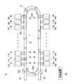
図1に示すように、実施形態の製造ライン10は、搬送装置12と、複数の加工装置70〜96と、エレベータ170〜196と、制御装置60を備えている。
As shown in FIG. 1, the
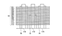
搬送装置12は、投入レール16と、周回レール18と、搬出レール20を備えている。周回レール18は、製造ライン10の中央部10aの周りを螺旋状に伸びている。周回レール18は、中央部10aの周りを同心状に13周している。したがって、図2に示すように、周回レール18は、13段のループ101〜113が積層された構造を備えている。なお、各ループ101〜113は、中央部10aの周りを1周する分のレールである。以下では、ループの段数を上から数える。すなわち、1段目のループという場合には、最上部のループ101を意味し、2段目のループという場合には、上から2段目のループ102を意味する。投入レール16は、周回レール18の上端部(すなわち、1段目のループ101)に接続されている。搬出レール20は、周回レール18の下端部(すなわち、13段目のループ113)に接続されている。投入レール16、周回レール18及び搬出レール20には、図3に示す搬送ベルト30が設けられている。搬送ベルト30は、レール上に載置された半導体ウエハを、レールに沿って移動させる。搬送ベルト30は、投入レール16側から搬出レール20側に向かって半導体ウエハを移動させる。したがって、投入レール16上に載置された半導体ウエハは、図1の矢印200に示すように、投入レール16から周回レール18の1段目のループ101に移動する。ループ101に移動した半導体ウエハは、図1の矢印202、204に示すように周回レール18を周回する。半導体ウエハは、各ループを1周する毎に下側のループに移動し、最終的に、13段目のループ113まで移動する。ループ113を周回したウエハは、矢印206に示すように、搬出レール20に搬出される。このように、半導体ウエハは、螺旋状に伸びる周回レール18に沿って周回しながら下側に移動する。したがって、1段目のループ101上に存在している半導体ウエハは1周目のウエハであり、2段目のループ102上に存在している半導体ウエハは2周目のウエハである。このように、ループの順序は、そのループ上の半導体ウエハが周回レール18上で周回している回数(以下、周回数という)と一致する。
The
図1に示すように、加工装置70〜96は、周回レール18に沿って配置されている。加工装置70〜96は、半導体ウエハに対して加工を行う。各加工装置70〜96は、洗浄装置、成膜装置、エッチング装置、イオン注入装置、または、その他の装置である。
As shown in FIG. 1, the
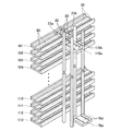
図1、3に示すように、各加工装置70〜96と周回レール18の間には、エレベータ170〜196が設置されている。また、周回レール18の各エレベータ170〜196に隣接する位置には、必要に応じてウエハ取出部22が形成されている。各エレベータと各ウエハ取出部の構造は略共通している。したがって、以下では、加工装置70の前方に位置するエレベータ170とウエハ取出部22の構造について説明する。
As shown in FIGS. 1 and 3,
図4、5に示すように、加工装置70の前方の周回レール18には、1段目のループ101と2段目のループ102にウエハ取出部22(すなわち、ウエハ取出部22a、22b)が形成されている。ウエハ取出部22では、搬送ベルト30が独立して設けられている。また、ウエハ取出部22には、周回レール18の幅方向にウエハを搬送する搬送ベルト32が設けられている。
As shown in FIGS. 4 and 5, the
図3〜5に示すように、エレベータ170は、鉛直方向に伸びる支柱と、ステージ170aを備えている。ステージ170aには、半導体ウエハを載置することができる。ステージ170aは、支柱に沿って高さ方向に移動することができる。ステージ170aには、搬送ベルト170bが設けられている。搬送ベルト170bは、搬送ベルト32と同一方向に半導体ウエハを搬送する。
As shown in FIGS. 3 to 5, the
図3、4に示すように、加工装置70内には、ローダ・アンローダ70aと、ロボットアーム70bと、加工用載置部70cが設置されている。ローダ・アンローダ70aには、搬送ベルト70dが設けられている。搬送ベルト70dは、搬送ベルト170bと同一方向に半導体ウエハを搬送する。ロボットアーム70bは、ローダ・アンローダ70aと加工用載置部70cの間で半導体ウエハを移動させる。加工装置70は、加工用載置部70c上に載置された半導体ウエハに対して加工を行う。
As shown in FIGS. 3 and 4, a loader /
製造ライン10では、周回レール18とエレベータ170〜196を用いて半導体ウエハを各加工装置70〜96の間で搬送し、各加工装置によって半導体ウエハに加工を行う。上述したウエハ取出部22は、周回レール18上からエレベータ170〜196に半導体ウエハを搬送するために用いられる。図6は、本実施形態の製造ライン10において、1つの半導体ウエハに対して行う加工工程の一覧を示している。図6に示すように、周回数が1周目の半導体ウエハに対しては、加工装置70、72、74、82、84、92、94及び96で加工が行われる。2周目の半導体ウエハに対しては、加工装置70、72、76、78、82、84、88及び96で加工が行われる。同様に、3周目以降の半導体ウエハに対しても、周回数に応じて使用される加工装置が定められている。図6の工程順は、半導体ウエハが周回レール18を1周する毎に、1つのレイヤーが形成されるように定められている。半導体ウエハが周回レール18を複数回周回することで、半導体ウエハに多数のレイヤーが形成される。これによって、半導体ウエハ中に半導体装置の構造が形成される。ウエハ取出部22は、図6の工程順に従って、半導体ウエハを各加工装置70〜96に搬送できるように設置されている。すなわち、図2に示すように、加工装置70では、1周目の半導体ウエハと2周目の半導体ウエハに対して加工が行われる。したがって、図4、5に示すように、加工装置70の前方の周回レール18には、1段目のループ101と2段目のループ102にウエハ取出部22が設けられている。同様に、加工装置72では、1周目の半導体ウエハと2周目の半導体ウエハに対して加工が行われる。したがって、加工装置72の前方の周回レール18には、1段目のループ101と2段目のループ102にウエハ取出部22が設けられている。加工装置76では、2周目の半導体ウエハと3周目の半導体ウエハと4周目の半導体ウエハに対して加工が行われる。したがって、加工装置74の前方の周回レール18には、2段目のループ102と3段目のループ103と4段目のループ104にウエハ取出部22が設けられている。このように、各加工装置の前方の周回レール18には、加工対象である周回数のウエハが流れるループにウエハ取出部22が設けられている。
In the
制御装置60は、搬送装置12と各エレベータ170〜196と各加工装置70〜96を制御する。周回レール18上から各加工装置70〜96に半導体ウエハを搬送するときに、制御装置60が各部を制御する方法について説明する。ここでは、例として、加工装置70に半導体ウエハを搬送するときの制御方法について説明する。
The
上述したように、周回レール18では、搬送ベルト30によって、半導体ウエハが下流側に搬送される。半導体ウエハが、図3〜5に示すウエハ取出部22a(加工装置70の前方の1段目のループ101に設けられたウエハ取出部22)に進入すると、図示しないセンサによって、ウエハ取出部22a内に半導体ウエハが進入したことが検出される。すると、制御装置60は、ウエハ取出部22a内の搬送ベルト30を停止させて、半導体ウエハをウエハ取出部22a内で停止させる。次に、制御装置60は、エレベータ170のステージ170aを、ウエハ取出部22aと同一の高さまで移動させる。次に、制御装置60は、ウエハ取出部22aの搬送ベルト32とステージ170aの搬送ベルト170bによって、半導体ウエハを、ウエハ取出部22a上からステージ170a上に移動させる。次に、制御装置60は、ステージ170aを下方に移動させ、加工装置70のローダ・アンローダ70aと同一の高さでステージ170aを停止させる。次に、制御装置60は、ステージ170aの搬送ベルト170bとローダ・アンローダ70aの搬送ベルト70dによって、半導体ウエハを、ステージ170a上からローダ・アンローダ70a上に移動させる。次に、制御装置60は、ロボットアーム70bによって、半導体ウエハを、ローダ・アンローダ70a上から加工用載置部70c上に移動させる。次に、制御装置60は、加工装置70によって、加工用載置部70c上の半導体ウエハに対して加工を行う。加工装置70による加工が完了すると、制御装置60は、ロボットアーム70bによって、半導体ウエハを、加工用載置部70c上からローダ・アンローダ70a上に移動させる。次に、制御装置60は、ローダ・アンローダ70aの搬送ベルト70dとステージ170aの搬送ベルト170bによって、半導体ウエハを、ローダ・アンローダ70a上からステージ170a上に移動させる。次に、制御装置60は、ステージ170aを上方に移動させ、ウエハ取出部22aと同一の高さでステージ170aを停止させる。次に、制御装置60は、ステージ170aの搬送ベルト170bとウエハ取出部22aの搬送ベルト32によって、半導体ウエハを、ステージ170a上からウエハ取出部22a上に移動させる。次に、制御装置60は、ウエハ取出部22aの搬送ベルト30によって、半導体ウエハをウエハ取出部22aから周回レール18の下流側に移動させる。
As described above, the semiconductor wafer is transported to the downstream side by the
同様に、半導体ウエハがウエハ取出部22b(加工装置70の前方の2段目のループ102に設けられたウエハ取出部22)内に進入した場合にも、図示しないセンサによって、半導体ウエハがウエハ取出部22b内に進入したことが検出される。すると、制御装置60は、ウエハ取出部22bの搬送ベルト32、エレベータ170、ローダ・アンローダ70a及びロボットアーム70bによって、ウエハ取出部22bから加工装置70の加工用載置部70c上に半導体ウエハを移動させ、加工装置70によって半導体ウエハに加工を行う。その後、制御装置60は、ウエハ取出部22bの搬送ベルト32、エレベータ170、ローダ・アンローダ70a及びロボットアーム70bによって、加工用載置部70c上からウエハ取出部22b上に半導体ウエハを移動させる。そして、搬送ベルト30によって、半導体ウエハをウエハ取出部22bから周回レール18の下流側に移動させる。
Similarly, when a semiconductor wafer enters the wafer take-out
以上に説明したように、ウエハ取出部22a、22b内に進入した半導体ウエハは、加工装置70内に搬入され、そこで半導体ウエハに対して加工が行わる。加工が完了した半導体ウエハは、元のウエハ取出部22(ウエハ取出部22aまたは22b)上に戻され、周回レール18の下流側に搬送される。加工装置70の前方の周回レール18には、1段目のループ101と2段目のループ102にウエハ取出部22が設けられている。したがって、図2に示すように、加工装置70で、1周目の半導体ウエハと2周目の半導体ウエハに対して加工が行われる。
As described above, the semiconductor wafer that has entered the wafer take-out
上述したウエハ取出部22a及び22b以外のウエハ取出部22に半導体ウエハが進入した場合にも、制御装置60は、同様に各部を制御する。これによって、何れかのウエハ取出部22に進入した半導体ウエハは、対応する加工装置内に搬入され、その加工装置内で加工を受け、その後、元のウエハ取出部22上に戻される。上述したように、ウエハ取出部22は、図2の表に従って、半導体ウエハを各加工装置に搬入できるように設置されている。したがって、周回レール18上を移動する半導体ウエハに対して、図2に示す順序で各加工装置により加工が行われる。これによって、半導体ウエハ中に半導体装置の構造が形成される。全ての加工が完了した半導体ウエハは、搬出レール20上に搬出される。搬出された半導体ウエハをダイシングすることで、半導体装置を製造することができる。
Even when a semiconductor wafer enters the wafer take-out
この製造ライン10では、周回レール18が螺旋状に伸びているので、各加工装置の前方に1段目から13段目までのループ101〜113が位置している。また、エレベータ等の搬送機構によって、必要なループ上から加工装置に半導体ウエハを搬送できるように構成されている。このため、1つの加工装置によって、1つの半導体ウエハに対して繰り返し加工を行うことができる。例えば、加工装置70によって、1周目の半導体ウエハ(すなわち、1段目のループ101上の半導体ウエハ)を加工することができるとともに、2周目の半導体ウエハ(すなわち、2段目のループ102上の半導体ウエハ)を加工することができる。このため、少ない加工装置で製造ライン10を構成することができ、設備投資に要する費用を抑えることができる。
In this
また、この製造ライン10では、多くの加工が行われた半導体ウエハほど周回レール18の下流側に存在している。すなわち、加工の程度が異なる半導体ウエハが周回レール18上で混在することがない。したがって、周回レール18上で半導体ウエハが汚染されることを抑制することができる。例えば、電極が形成されている半導体ウエハと加工前の半導体ウエハがレール上で混在していると、レール上で加工前の半導体ウエハが汚染される。すなわち、電極が形成されている半導体ウエハがレール上を移動すると、そのレールに電極の構成材料である金属が極微量に付着する。その後にそのレール上に加工前の半導体ウエハが進入すると、レールに付着している金属(電極の構成材料である金属)が加工前の半導体ウエハに付着する。金属が付着した状態で半導体ウエハに加工(例えば、熱処理等)が行われると、半導体ウエハの内部に金属が拡散し、半導体ウエハの特性が変化してしまう。本実施形態の製造ライン10では、加工の程度が異なるウエハが周回レール18上で混在することが無いので、このような汚染を抑制することができる。したがって、半導体ウエハの特性が変化することを抑制することができ、安定した品質で半導体装置を製造することができる。
Further, in the
また、本実施形態の製造ライン10では、加工の程度が異なる半導体ウエハが周回レール18上に混在することがないので、各部の制御を単純化することができる。例えば、加工の程度が異なる半導体ウエハが周回レール上に混在する場合には、ある半導体ウエハがウエハ取出部22に進入したときに、その半導体ウエハに対してどの程度加工が行われているのかを特定し、その半導体ウエハに対して加工を行うべきか否かを判定する必要が生じる。しかしながら、本実施形態の製造ライン10では、加工の程度が異なる半導体ウエハがレール上に混在することがないので、このような判定を行う必要がない。ウエハ取出部22に進入した半導体ウエハの全てを対応する加工装置で加工すればよい。複雑な制御が不要となるので、本実施形態の製造ライン10では、容易に製造ライン10を管理することができる。
Further, in the
なお、上述した実施例では、搬送ベルト30によって、各半導体ウエハを単体で搬送するように搬送装置12が構成されていた。しかしながら、搬送装置12は、レールに沿って移動するトレーを有していてもよい。この場合には、各トレー上に半導体ウエハを載置し、トレーと共に半導体ウエハをレールに沿って移動させることができる。このような構成でも、搬出レール20に搬出されたトレーを洗浄し、洗浄後のトレーに半導体ウエハを載置して投入レール16に投入することで、周回レール18上での半導体ウエハの汚染を抑制することができる。
In the embodiment described above, the
以上、本発明の具体例を詳細に説明したが、これらは例示にすぎず、特許請求の範囲を限定するものではない。特許請求の範囲に記載の技術には、以上に例示した具体例をさまざまに変形、変更したものが含まれる。
本明細書または図面に説明した技術要素は、単独であるいは各種の組み合わせによって技術的有用性を発揮するものであり、出願時請求項記載の組み合わせに限定されるものではない。また、本明細書または図面に例示した技術は複数目的を同時に達成するものであり、そのうちの一つの目的を達成すること自体で技術的有用性を持つものである。
Specific examples of the present invention have been described in detail above, but these are merely examples and do not limit the scope of the claims. The technology described in the claims includes various modifications and changes of the specific examples illustrated above.
The technical elements described in this specification or the drawings exhibit technical usefulness alone or in various combinations, and are not limited to the combinations described in the claims at the time of filing. In addition, the technology illustrated in the present specification or the drawings achieves a plurality of objects at the same time, and has technical utility by achieving one of the objects.
10:製造ライン
10a:中央部
12:搬送装置
16:投入レール
18:周回レール
20:搬出レール
22:ウエハ取出部
22a:ウエハ取出部
22b:ウエハ取出部
30:搬送ベルト
32:搬送ベルト
60:制御装置
70〜96:加工装置
70a:ローダ・アンローダ
70b:ロボットアーム
70c:加工用載置部
70d:搬送ベルト
101〜113:ループ
170〜196:エレベータ
170a:ステージ
170b:搬送ベルト
DESCRIPTION OF SYMBOLS 10:
Claims (2)
複数回周回するように伸びる移動経路に沿ってウエハを搬送する搬送手段と、
複数の加工装置、
を備えており、
各加工装置は、前記移動経路上のウエハを取り込み、取り込んだウエハに加工を行い、加工後のウエハを前記移動経路上に戻すように構成されており、
少なくとも1つの加工装置は、前記移動経路のうちの第1のループ上のウエハを取り込み、取り込んだウエハに加工を行い、加工後のウエハを第1のループ上に戻すように構成されているとともに、前記移動経路のうちの第1のループとは異なる第2のループ上のウエハを取り込み、取り込んだウエハに加工を行い、加工後のウエハを第2のループ上に戻すように構成されている、
ことを特徴とする製造ライン。 A production line for semiconductor devices,
A transfer means for transferring the wafer along a movement path extending so as to circulate a plurality of times;
Multiple processing equipment,
With
Each processing apparatus is configured to take a wafer on the movement path, process the taken wafer, and return the processed wafer to the movement path.
At least one processing apparatus is configured to take in the wafer on the first loop in the movement path, process the taken wafer, and return the processed wafer to the first loop. The wafer on the second loop different from the first loop in the moving path is taken in, processed on the taken-in wafer, and the processed wafer is returned to the second loop. ,
A production line characterized by that.
Priority Applications (1)
| Application Number | Priority Date | Filing Date | Title |
|---|---|---|---|
| JP2010254202A JP2012104761A (en) | 2010-11-12 | 2010-11-12 | Manufacturing line of semiconductor device |
Applications Claiming Priority (1)
| Application Number | Priority Date | Filing Date | Title |
|---|---|---|---|
| JP2010254202A JP2012104761A (en) | 2010-11-12 | 2010-11-12 | Manufacturing line of semiconductor device |
Publications (1)
| Publication Number | Publication Date |
|---|---|
| JP2012104761A true JP2012104761A (en) | 2012-05-31 |
Family
ID=46394789
Family Applications (1)
| Application Number | Title | Priority Date | Filing Date |
|---|---|---|---|
| JP2010254202A Pending JP2012104761A (en) | 2010-11-12 | 2010-11-12 | Manufacturing line of semiconductor device |
Country Status (1)
| Country | Link |
|---|---|
| JP (1) | JP2012104761A (en) |
Cited By (6)
| Publication number | Priority date | Publication date | Assignee | Title |
|---|---|---|---|---|
| CN104495269A (en) * | 2014-12-19 | 2015-04-08 | 苏州互强工业设备有限公司 | Automatic assembly line |
| JP2016149437A (en) * | 2015-02-12 | 2016-08-18 | 株式会社ディスコ | Wafer processing system |
| CN109216250A (en) * | 2018-10-19 | 2019-01-15 | 清华大学 | wafer transfer mechanism |
| JP2020501217A (en) * | 2016-09-09 | 2020-01-16 | ザ プロクター アンド ギャンブル カンパニーThe Procter & Gamble Company | System and method for manufacturing customized products with mass-produced products |
| US11584628B2 (en) | 2016-09-09 | 2023-02-21 | The Procter & Gamble Company | System and method for independently routing vehicles and delivering containers and closures to unit operation systems |
| US11698626B2 (en) | 2016-09-09 | 2023-07-11 | The Procter & Gamble Company | System and method for producing products based upon demand |
-
2010
- 2010-11-12 JP JP2010254202A patent/JP2012104761A/en active Pending
Cited By (13)
| Publication number | Priority date | Publication date | Assignee | Title |
|---|---|---|---|---|
| CN104495269A (en) * | 2014-12-19 | 2015-04-08 | 苏州互强工业设备有限公司 | Automatic assembly line |
| TWI691012B (en) * | 2015-02-12 | 2020-04-11 | 日商迪思科股份有限公司 | Wafer processing system |
| KR20160099479A (en) * | 2015-02-12 | 2016-08-22 | 가부시기가이샤 디스코 | Wafer processing system |
| CN105895569A (en) * | 2015-02-12 | 2016-08-24 | 株式会社迪思科 | Wafer processing system |
| JP2016149437A (en) * | 2015-02-12 | 2016-08-18 | 株式会社ディスコ | Wafer processing system |
| CN105895569B (en) * | 2015-02-12 | 2020-10-09 | 株式会社迪思科 | Wafer processing system |
| KR102380422B1 (en) | 2015-02-12 | 2022-03-31 | 가부시기가이샤 디스코 | Wafer processing system |
| JP2020501217A (en) * | 2016-09-09 | 2020-01-16 | ザ プロクター アンド ギャンブル カンパニーThe Procter & Gamble Company | System and method for manufacturing customized products with mass-produced products |
| JP2021108150A (en) * | 2016-09-09 | 2021-07-29 | ザ プロクター アンド ギャンブル カンパニーThe Procter & Gamble Company | System and method for producing customized products with mass-produced products |
| JP7092748B2 (en) | 2016-09-09 | 2022-06-28 | ザ プロクター アンド ギャンブル カンパニー | Systems and methods for manufacturing customized products with mass-produced products |
| US11584628B2 (en) | 2016-09-09 | 2023-02-21 | The Procter & Gamble Company | System and method for independently routing vehicles and delivering containers and closures to unit operation systems |
| US11698626B2 (en) | 2016-09-09 | 2023-07-11 | The Procter & Gamble Company | System and method for producing products based upon demand |
| CN109216250A (en) * | 2018-10-19 | 2019-01-15 | 清华大学 | wafer transfer mechanism |
Similar Documents
| Publication | Publication Date | Title |
|---|---|---|
| JP2012104761A (en) | Manufacturing line of semiconductor device | |
| KR101516819B1 (en) | Substrate treatment apparatus | |
| KR100514624B1 (en) | Substrate sorting device and method | |
| CN105990202B (en) | Substrate processing apparatus and substrate processing method | |
| CN105374725A (en) | Joint device, joint system, and joint method | |
| KR101930555B1 (en) | Substrate processing system, substrate processing method and storage medium for computer | |
| JP5025231B2 (en) | Substrate transfer processing equipment | |
| KR102479206B1 (en) | Substrate processing device and substrate transfer method | |
| JP4280159B2 (en) | Substrate processing equipment | |
| KR102309933B1 (en) | Substrate processing system | |
| KR102000013B1 (en) | Apparatus and method for treating substrates | |
| JP2012146714A (en) | Component mounting device | |
| JP6123740B2 (en) | Semiconductor device manufacturing line and semiconductor device manufacturing method | |
| JP2006332558A (en) | Substrate processing system | |
| CN108100666A (en) | The control method of control method and substrate the supply retracting device of substrate feeding device | |
| JP5606546B2 (en) | Work processing device | |
| CN105374709A (en) | Engagement device, engagement system and engagement method | |
| JP2010041059A (en) | Coating and developing apparatus | |
| KR102037900B1 (en) | Apparatus and method for treating substrates | |
| KR102231176B1 (en) | Apparatus for transferring articles | |
| JP2009239000A (en) | Substrate treatment system | |
| KR102259067B1 (en) | Substrate Processing Apparatus and Substrate Transfer Method | |
| JP7399552B2 (en) | Container transport device and laser processing device | |
| CN106796873A (en) | Semiconductor plasma washing equipment | |
| JP7347658B2 (en) | Substrate processing equipment and substrate processing method |