JP2012104745A - Laminated electronic component and method for manufacturing laminated electronic component - Google Patents
Laminated electronic component and method for manufacturing laminated electronic component Download PDFInfo
- Publication number
- JP2012104745A JP2012104745A JP2010253829A JP2010253829A JP2012104745A JP 2012104745 A JP2012104745 A JP 2012104745A JP 2010253829 A JP2010253829 A JP 2010253829A JP 2010253829 A JP2010253829 A JP 2010253829A JP 2012104745 A JP2012104745 A JP 2012104745A
- Authority
- JP
- Japan
- Prior art keywords
- bottom electrode
- laminate
- electrode
- electronic component
- end surface
- Prior art date
- Legal status (The legal status is an assumption and is not a legal conclusion. Google has not performed a legal analysis and makes no representation as to the accuracy of the status listed.)
- Granted
Links
Images

Landscapes
- Manufacturing Cores, Coils, And Magnets (AREA)
- Coils Or Transformers For Communication (AREA)
Abstract
Description
本発明は、積層型電子部品及び積層型電子部品の製造方法に関するものである。 The present invention relates to a multilayer electronic component and a method for manufacturing the multilayer electronic component.
従来の積層型電子部品として、絶縁体層と導体パターンとが積層され内部にコイル導体が形成された積層体と、積層体の底面に露出すると共に、積層体の端面側に配置される底面電極と、積層体の端面を覆うように形成されると共に、コイル導体及び底面電極と電気的に接続される外部電極と、を備えるものが知られている(例えば、特許文献1参照)。この積層型電子部品では、底面電極における積層体の端面側の端部は、積層体の端面と一致するように配置されている。すなわち、コイル導体の引出導体の端部と同様に、底面電極の端部が積層体の端面から露出している。 As a conventional multilayer electronic component, a laminate in which an insulator layer and a conductor pattern are laminated and a coil conductor is formed inside, and a bottom electrode that is exposed on the bottom surface of the laminate and is disposed on the end face side of the laminate And an external electrode that is formed so as to cover the end face of the laminated body and that is electrically connected to the coil conductor and the bottom electrode (see, for example, Patent Document 1). In this multilayer electronic component, the end of the bottom electrode on the end surface side of the multilayer body is disposed so as to coincide with the end surface of the multilayer body. That is, the end portion of the bottom electrode is exposed from the end surface of the multilayer body, similarly to the end portion of the lead conductor of the coil conductor.
ここで、金属部分と絶縁体層の部分とで熱収縮率に差があるため、積層体の焼成時において、底面電極と積層体の絶縁体層からなる部分との間に収縮差が生じる。従来の積層型電子部品では、底面電極の端部が積層体の端面にまで及んでいるため、焼成後は、図3(b)に示すように、積層体の外形が歪み、積層体の端面に対して底面電極が出っ張る構成となっていた。このような積層体に対して、例えばディップ法などによって導体ペーストを塗布する場合、出っ張った底面電極によって導体ペーストが底面側へ回り込み難くなる。無理に底面側へ回り込ませようとした場合は導体ペーストへの浸漬の深さを深くする必要があるが、その結果、導体ペーストの回り込み量が必要以上に大きくなってしまう可能性がある。また、底面電極は絶縁体層からなる部分に比べて研磨され難く、従来の積層型電子部品では、底面電極が配置されている角部を面取りして丸みを形成し難いという問題がある。このように角部に丸みを形成し難いため、更に導体ペーストが底面側に回り込み難くなる。 Here, since there is a difference in thermal shrinkage between the metal portion and the insulator layer portion, a shrinkage difference occurs between the bottom electrode and the portion of the laminate made of the insulator layer during firing of the laminate. In the conventional multilayer electronic component, since the end portion of the bottom electrode reaches the end surface of the multilayer body, the outer shape of the multilayer body is distorted after firing as shown in FIG. In contrast, the bottom electrode protrudes. When a conductor paste is applied to such a laminate by, for example, a dip method, the conductor paste is unlikely to wrap around the bottom surface due to the protruding bottom electrode. When it is attempted to forcibly wrap around the bottom surface, it is necessary to increase the depth of immersion in the conductor paste. As a result, the amount of wraparound of the conductor paste may become larger than necessary. Further, the bottom electrode is harder to be polished than the portion made of the insulator layer, and the conventional multilayer electronic component has a problem that it is difficult to chamfer the corner portion where the bottom electrode is disposed to form a round shape. Thus, since it is difficult to form roundness at the corners, the conductive paste further hardly goes around to the bottom surface side.
本発明は、このような問題を解決するためになされたものであり、外部電極を形成するための導体ペーストを底面側に回り込み易くすると共に、回り込み量を抑制することのできる積層型電子部品及び積層型電子部品の製造方法を提供することを目的とする。 The present invention has been made to solve such a problem, and makes it easy to wrap around the conductive paste for forming the external electrode to the bottom surface side, and a multilayer electronic component capable of suppressing the amount of wraparound, and It is an object of the present invention to provide a method for manufacturing a multilayer electronic component.
本発明に係る積層型電子部品は、絶縁体層と導体パターンとが積層され内部にコイル導体が形成された積層体と、積層体の底面に露出すると共に、積層体の端面側に配置される底面電極と、積層体の端面を覆うように形成されると共に、コイル導体及び底面電極と電気的に接続される外部電極と、を備え、積層体の積層方向から見て、底面電極における端面側の端部は、端面から離間していることを特徴とする。 The multilayer electronic component according to the present invention includes a multilayer body in which an insulator layer and a conductor pattern are laminated and a coil conductor is formed therein, and is exposed on the bottom surface of the multilayer body and disposed on the end face side of the multilayer body. The bottom electrode and an external electrode that is formed so as to cover the end surface of the multilayer body and that is electrically connected to the coil conductor and the bottom electrode, and viewed from the stacking direction of the multilayer body, the end surface side of the bottom electrode The end of is spaced from the end face.
本発明に係る積層型電子部品では、積層体の積層方向から見て、底面電極における端面側の端部が、積層体の端面から離間している。すなわち、底面電極の端部と積層体の端面との間には絶縁体層からなる部分が存在する。従って、積層体の端面と底面との間の角部も、端面の他の領域と同じように収縮し、底面電極の部分のみ出っ張ることが防止される。更に、積層体の端面と底面との間の角部は絶縁体層によって構成されるため、研磨され易い。その結果、積層体の底面に底面電極を形成しても、角部を面取りして丸みを形成することができる。従って、外部電極を形成するときに積層体の端面を導体ペーストに浸漬させる際、端面付近を僅かに浸漬させるだけでも、導体ペーストは底面電極付近の角部で引っ張られることなくスムーズに底面側に回り込むことができる。導体ペーストがスムーズに底面側に回り込むことができるため、積層体を必要以上に浸漬させる必要がなく、これによって、外部電極の底面側への回り込み量を所望の大きさに抑えることができる。以上によって、外部電極を形成するための導体ペーストを底面側に回り込み易くすると共に、回り込み量を抑制することができる。 In the multilayer electronic component according to the present invention, when viewed from the stacking direction of the multilayer body, the end portion on the end surface side of the bottom electrode is separated from the end surface of the multilayer body. That is, a portion made of an insulator layer exists between the end portion of the bottom electrode and the end surface of the multilayer body. Accordingly, the corner portion between the end face and the bottom face of the laminate is also contracted in the same manner as the other areas of the end face, and only the bottom electrode portion is prevented from protruding. Furthermore, since the corner | angular part between the end surface and bottom face of a laminated body is comprised with an insulator layer, it is easy to grind | polish. As a result, even if the bottom electrode is formed on the bottom surface of the laminate, the corners can be chamfered to form roundness. Therefore, when the end face of the laminate is immersed in the conductor paste when forming the external electrode, the conductor paste is smoothly pulled to the bottom side without being pulled at the corner near the bottom electrode even if the end face is slightly immersed. I can wrap around. Since the conductive paste can smoothly wrap around to the bottom surface side, it is not necessary to immerse the laminate more than necessary, whereby the amount of wraparound of the external electrode to the bottom surface side can be suppressed to a desired size. As described above, the conductor paste for forming the external electrode can be easily circulated to the bottom surface side, and the amount of wraparound can be suppressed.
また、本発明に係る積層型電子部品において、底面電極は、積層体の底面から突出していることが好ましい。例えば、底面電極の外面が積層体の底面と一致していた場合、底面側においては外部電極の回り込み部のみが下方に突出した構成となる。このような構成では、積層型電子部品を基板などに実装する際、外部電極の回り込み部だけが基板の端子電極と接触し、実装時のバランスが悪くなる。一方、底面電極が積層体の底面から突出すると、外部電極の回り込み部と底面電極の広い領域で基板の端子電極と接触することができるため、実装時のバランスが良くなる。 In the multilayer electronic component according to the present invention, it is preferable that the bottom electrode protrudes from the bottom surface of the multilayer body. For example, when the outer surface of the bottom electrode coincides with the bottom surface of the laminated body, only the wraparound portion of the external electrode protrudes downward on the bottom surface side. In such a configuration, when the multilayer electronic component is mounted on a substrate or the like, only the wraparound portion of the external electrode comes into contact with the terminal electrode of the substrate, resulting in a poor balance during mounting. On the other hand, when the bottom electrode protrudes from the bottom surface of the laminate, it can come into contact with the terminal electrode of the substrate in a wide area of the external electrode wrapping portion and the bottom electrode, so that the balance during mounting is improved.
本発明に係る積層型電子部品の製造方法は、絶縁体層と導体パターンとが積層され内部にコイル導体が形成された積層体と、積層体の底面に露出すると共に、積層体の端面側に配置される底面電極と、積層体の端面を覆うように形成されると共に、コイル導体及び底面電極と電気的に接続される外部電極と、を備える積層型電子部品の製造方法であって、積層体の積層方向から見て、端面側の端部が、端面から離間する位置に底面電極を形成する底面電極形成工程と、端面に導体ペーストを塗布することによって外部電極を形成する外部電極形成工程と、を備えることを特徴とする。 The method for manufacturing a multilayer electronic component according to the present invention includes a laminate in which an insulator layer and a conductor pattern are laminated and a coil conductor is formed therein, and is exposed on the bottom surface of the laminate, and on the end face side of the laminate. A method of manufacturing a multilayer electronic component comprising: a bottom electrode to be disposed; and an external electrode formed so as to cover an end surface of the multilayer body and electrically connected to the coil conductor and the bottom electrode. A bottom electrode forming step for forming a bottom electrode at a position where the end on the end surface side is separated from the end surface as viewed from the body stacking direction, and an external electrode forming step for forming an external electrode by applying a conductive paste to the end surface And.
本発明に係る積層型電子部品の製造方法によれば、上述のような本発明に係る積層型電子部品と同様の作用・効果を得ることができ、外部電極を形成するための導体ペーストを底面側に回り込み易くすると共に、回り込み量を抑制することができる。 According to the method for manufacturing a multilayer electronic component according to the present invention, the same operation and effect as the multilayer electronic component according to the present invention as described above can be obtained, and the conductive paste for forming the external electrode is formed on the bottom surface. While making it easy to wrap around, the amount of wraparound can be suppressed.
本発明によれば、外部電極を形成するための導体ペーストを底面側に回り込み易くすると共に、回り込み量を抑制することができる。 ADVANTAGE OF THE INVENTION According to this invention, while making it easy to wrap around the conductor paste for forming an external electrode to the bottom face side, the amount of wraparound can be suppressed.
以下、本発明に係る積層型電子部品の好適な実施形態として積層型インダクタについて、図面を参照して詳細に説明する。 Hereinafter, a multilayer inductor as a preferred embodiment of a multilayer electronic component according to the present invention will be described in detail with reference to the drawings.
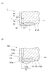
図1は、本発明に係る積層型電子部品として積層型インダクタの実施形態を示す断面図及び底面図である。 FIG. 1 is a cross-sectional view and a bottom view showing an embodiment of a multilayer inductor as a multilayer electronic component according to the present invention.
積層型電子部品1は、図1に示されるように、略直方体形状の積層体2と、積層体2の内部に形成されたコイル導体3と、積層体2の両端に形成される外部電極4,6と、積層体2の底面に形成される底面電極7,8と、を備えている。
As shown in FIG. 1, the multilayer
積層体2は、複数の絶縁体層5と導体パターン3A,3B,3Cとを積層することによって形成され、内部にコイル導体3を有している。積層体2は、焼成後に絶縁体層5となる複数の絶縁体グリーンシートと、当該絶縁体グリーンシート上に形成された導体パターン3A,3B,3Cと、導体パターン3A,3B,3Cをそれぞれ電気的に接続するスルーホール電極(不図示)とにより構成される。なお、焼成された実際の積層型電子部品1は、絶縁体層5の境界が視認できない程度に一体化さている。絶縁体層5は、例えば、ストロンチウム、カルシウム、アルミナ及び酸化珪素からなるガラスと、アルミナとからなるガラス系セラミックから構成されている。フェライト(例えば、Ni−Cu−Zn系フェライト、Ni−Cu−Zn−Mg系フェライト、Cu−Zn系フェライト、またはNi−Cu系フェライト)から構成されていてもよい。
The
積層体2は、直方体状をなしており、上面2aと、上面2aと対向する底面2bと、長手方向に互いに対向する端面2c,2dと、上面2aと底面2bとを連結して短手方向に互いに対向する側面2e,2fと、を備えている。なお、底面2bとは、積層型電子部品1を基板に実装する際に、基板に対する実装面となる面である。
The
コイル導体3は、積層体2の内部に形成され、導体パターン3A,3B,3Cとスルーホール電極とで複数ターンに巻回されている。具体的に、コイル導体3は、一枚の絶縁体層5上で1ターン以下のコイルパターンを形成する導体パターン3Bと、積層方向に隣接する他の絶縁体層5上の導体パターン3Bとをスルーホール電極で電気的に接続することにより、形成されている。また、コイル導体3は、導体パターン3Bによるコイル部の端部より積層体2の端面2cに引き出された引出導体パターン3Aと、端面2dに引き出された引出導体パターン3Cと、を有している。コイル導体3を構成する材料として、銀や銅を用いることができる。
The
各外部電極4,6は、積層体2の端面2c,2dを覆うように形成されている。外部電極4は、積層体2の端面2c全体を覆う主部4aと、積層体2の底面2b側に回り込んで底面電極7と電気的に接続される回り込み部4bと、積層体2の上面2a及び側面2e,2d側に回り込んだ回り込み部4cと、を備えている。外部電極6は、積層体2の端面2d全体を覆う主部6aと、積層体2の底面2b側に回り込んで底面電極8と電気的に接続される回り込み部6bと、積層体2の上面2a及び側面2e,2d側に回り込んだ回り込み部6cと、を備えている。このような構成により、外部電極4は、コイル導体3と底面電極7とを電気的に接続し、外部電極6は、コイル導体3と底面電極8とを電気的に接続する。外部電極4,6は、ディップ法により形成されている。すなわち、積層体2の端面2c,2dを導体ペースト中に浸漬させて引き抜くことによって導体ペーストを塗布し、焼成することで外部電極4,6を形成する。外部電極4,6を構成する材料として、銀や銅を用いることができる。外部電極4,6の表面にはめっきが施されている。
Each
本実施形態では、底面電極7,8が形成されていることにより、外部電極4,6の回り込み量は極めて小さくされている。外部電極4の回りこみ量とは、図3(a)においてB1で示されるように、積層体2の端面2cと、回り込み部4b,4cにおける他方の端面2d側の端部との間の距離である。外部電極6の回り込み量とは、積層体2の端面2dと、回り込み部6b,6cにおける他方の端面2c側の端部との間の距離である。本実施形態に係る積層型電子部品1のサイズは、一例として、0.6mm(長さ)×0.3mm(幅)×0.3mm(高さ)に設定される。このようなサイズの場合、回り込み量は、焼成後において、40〜110μmとすることが好ましい。40μm以上とすることによって、回り込み部分をフィレット形成部とすることができるため、実装強度を高めることができる。110μm以下とすることによって、材料コストを抑制することができる。ただし、好ましい回り込み量は、積層型電子部品1のサイズによって異なる。コイル導体3との関係においては、積層方向から見て、外部電極4の回り込み部4b,4cが、コイルパターンを形成している導体パターン3B(積層体2の端面2cに沿って延びている部分)と重ならない程度の大きさとされていることが好ましい。また、積層方向から見て、外部電極6の回り込み部6b,6cが、コイルパターンを形成している導体パターン3B(積層体2の端面2dに沿って延びている部分)と重ならない程度の大きさとされていることが好ましい。
In the present embodiment, since the
底面電極7は、積層体2の底面2bにおける端面2c側に配置され、矩形状に広がる電極である。底面電極7は、底面2bよりも下方に突出している。実装時において、基板の外部電極との接続性を確保するため、底面電極7における端面2d側の端部7bは、端面2d側に十分に延びている。本実施形態では、底面電極7の端部7bは、導体パターン3Bによって形成されるコイルパターンの内側にまで延びている。底面電極7の端部7cは積層体2の側面2eから離間しており、端部7dは積層体2の側面2fから離間している。これによって、積層体2の焼成後に、底面電極7の端部7c,7dが側面2e,2fから出っ張ることが防止される。また、端部7c,7dは、側面2e,2fと面一であってもよい。この場合、電極面積を大きく確保して、実装強度を上げることができる。底面電極7を構成する材料として、銀や銅を用いることができる。
The
積層方向から見て、底面電極7における端面2c側の端部7aは、端面2cから離間している。これによって、端面2cと底面電極7の端部7aとの間には、隙間が形成される(図3(a)においてGPで示す)。この隙間が小さすぎる場合は、積層体2の焼成時に底面電極7が積層体2の端面2cより出っ張ってしまう。一方、この隙間が大きすぎる場合は、外部電極4と底面電極7とを電気的に接続するために、回り込み部4b,4cの回り込み量を大きくしなくてはならない。従って、端面2cと底面電極7の端部7aとの間の隙間の大きさは、焼成前は10〜50μmとすることが好ましい。焼成後は3〜30μmとすることが好ましく、5〜20μmとすることが更に好ましい。本実施形態では、底面電極7の端部7aは、積層方向から見て、端面2cとコイルパターンを形成する導体パターン3B(積層体2の端面2cに沿って延びている部分)との間に配置されている。
When viewed from the stacking direction, the
底面電極8は、積層体2の底面2bにおける端面2d側に配置され、矩形状に広がる電極である。底面電極8は、底面2bよりも下方に突出している。実装時において、基板の外部電極との接続性を確保するため、底面電極8における端面2c側の端部8bは、端面2c側に十分に延びている。本実施形態では、底面電極8の端部8bは、導体パターン3Bによって形成されるコイルパターンの内側にまで延びている。底面電極8の端部8cは積層体2の側面2eから離間しており、端部8dは積層体2の側面2fから離間している。これによって、積層体2の焼成後に、底面電極8の端部8c,8dが側面2e,2fから出っ張ることが防止される。また、端部8c,8dは、側面2e,2fと面一であってもよい。この場合、電極面積を大きく確保して、実装強度を上げることができる。底面電極8を構成する材料として、銀や銅を用いることができる。
The
積層方向から見て、底面電極8における端面2d側の端部8aは、端面2dから離間している。これによって、端面2dと底面電極8の端部8aとの間には、隙間が形成される。この隙間が小さすぎる場合は、積層体2の焼成時に底面電極8が積層体2の端面2dより出っ張ってしまう。一方、この隙間が大きすぎる場合は、外部電極6と底面電極8とを電気的に接続するために、回り込み部4b,4cの回り込み量を大きくしなくてはならない。従って、端面2dと底面電極8の端部8aとの間の隙間の大きさは、焼成前は10〜50μmとすることが好ましい。焼成後は3〜30μmとすることが好ましく、5〜20μmとすることが更に好ましい。本実施形態では、底面電極8の端部8aは、積層方向から見て、端面2dとコイルパターンを形成する導体パターン3B(積層体2の端面2dに沿って延びている部分)との間に配置されている。
When viewed from the stacking direction, the
このように、底面電極7,8が端面2c,2dより離間しているため、積層体2における端面2cと底面2bとの間の角部、及び端面2dと底面2bとの間の角部は、絶縁体層5による絶縁体部分が配置される構成となる。従って、研磨によって角部を除去して丸みを形成することにより、端面2cと底面電極7の端部7aとの間、及び端面2dと底面電極8の端部8aとの間には、所定の曲率半径を有する面取部R2が形成される。なお、積層体2における他の角部にも所定の曲率半径を有する面取部R1が形成される。
Thus, since the
次に、図2を参照して、上述した構成の積層型電子部品1の製造方法について説明する。
Next, a method for manufacturing the multilayer
図2に示すように、積層型電子部品1は、積層体2を形成する積層体準備工程S1が行われた後、積層体2に外部電極4,6を形成する外部電極形成工程S6が行われることによって製造される。積層体準備工程S1においては、まず、コイル導体3を形成するコイル導体形成工程S2が実行される。コイル導体形成工程S2では、ドクターブレード法などにより絶縁体層5となる絶縁体グリーンシートを準備し、当該絶縁体グリーンシート上に、導体パターン3A,3B,3Cの形状になるように導体ペーストをそれぞれスクリーン印刷などによって塗布し、乾燥することによって焼成前の導体パターン3A,3B,3Cを形成する。また、積層方向に接続する部分にスルーホールを形成すると共に導体ペーストを充填してスルーホール電極を形成しながら、各絶縁体グリーンシートを重ね合わせることで、焼成前のコイル導体3を形成する。
As shown in FIG. 2, in the multilayer
次に、底面電極7,8を形成する底面電極形成工程S3を実行する。底面電極形成工程S3では、最下層の絶縁体層5となる絶縁体グリーンシートにおける底面2bに対応する面に、底面電極7,8の形状になるように導体ペーストをそれぞれスクリーン印刷などによって塗布し、乾燥することによって焼成前の底面電極7,8を形成する。このとき、底面電極7,8の端部7a,8aが積層体2の端面2c,2d(絶縁体グリーンシートの積層物を切断して積層体2のチップを形成する場合は、端面2c,2dに対応する切断予定位置)から離間する位置に導体ペーストを塗布する。なお、底面電極7,8は、各絶縁体グリーンシートを積層する前に形成してもよく(この場合は、コイル導体形成工程S2と底面電極形成工程S3が同時に行われる)、絶縁体グリーンシートを積層した後に形成してもよい。コイル導体形成工程S2と底面電極形成工程S3の後、絶縁体グリーンシートの積層物をそれぞれの積層体2の大きさのチップとなるように切断する。
Next, a bottom electrode forming step S3 for forming the
次に、積層体2の角部を除去して面取りを行う角部除去工程S4を実行する。角部除去工程S4では、ポリエチレン等の材料からなる密閉回転ポットに水と複数の積層体2のチップと研磨用のメディアを入れて、この密閉回転ポットを回転させることによって、積層体2のチップの角部分の面取りが行われる。これによって、それぞれの角部が所定の曲率半径を有し、面取部R1,R2が形成される(バレル研磨)。次に、積層体2を焼成する焼成工程S5を実行する。焼成工程S5では、面取り加工を施した積層体2のチップに所定温度で所定時間加熱処理を施すことによって脱バインダを行う。脱バインダを行った後、更に高温で加熱して焼成を行うことでコイル導体3及び底面電極7,8が形成された積層体2を得る。以上の処理によって、積層体準備工程S1が終了する。
Next, a corner removal step S4 for chamfering by removing the corner of the
積層体準備工程S1の後、外部電極4,6を形成するための導体ペーストを塗布用プレート上に載せたものを準備し、複数の積層体2を保持具で保持する。積層体2の端面2cが下方を向くように配置すると共に、端面2cを塗布用プレート上の導体ペースト中に浸漬させて引き上げることによって、端面2cに導体ペーストを塗布する。このとき、外部電極4の回り込み量が大きくならないように、端面2cを導体ペーストの液面に僅かに接触させる程度の浸漬深さに留める。このように浸漬深さを僅かとしても、本実施形態における積層体2では、外部電極4を十分に底面電極7と接続させることができる。導体ペーストを塗布した後、乾燥させて硬化させて焼成前の外部電極4を形成する。その後、端面2d側においても同様に浸漬し乾燥することで、焼成前の外部電極6を形成する。その後、焼成することによって外部電極4,6を積層体2に焼き付ける。焼き付けた後、外部電極4,6の表面にめっき処理を施す。以上によって、図2に示す工程が終了し、積層型電子部品1を得ることができる。
After the multilayer body preparation step S1, a conductor paste for forming the
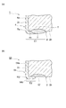
次に、本実施形態に係る積層型電子部品1の作用・効果について、図3を参照して説明する。図3(a)は、図1(a)に示す積層型電子部品1の底面電極7付近の構成を示す拡大図である。図3(b)は、従来の積層型電子部品100の底面電極107の構成を示す拡大図である。
Next, the operation and effect of the multilayer
図3(b)に示すように、従来の積層型電子部品100では、底面電極107が、積層体102の端面102cに露出している。すなわち、底面電極107の端部107aが積層体2の端面102cにまで及んでおり、焼成前において端部107aの位置が端面102cと一致している。
As shown in FIG. 3B, in the conventional multilayer
ここで、金属部分と絶縁体層の部分とで熱収縮率に差があるため、積層体102の焼成時において、底面電極107と積層体102の絶縁体層105からなる部分との間に収縮差が生じる。従来の積層型電子部品100では、底面電極107の端部107aが積層体102の端面102cにまで及んでいるため、焼成後は、図3(b)に示すように、積層体102の外形が歪み、積層体102の端面102cに対して底面電極107が出っ張る構成となっていた。
Here, since there is a difference in thermal shrinkage between the metal portion and the insulator layer portion, the shrinkage between the
このような従来の積層型電子部品100の積層体102に対して、例えばディップ法などによって導体ペーストを塗布して外部電極104を形成する場合、出っ張った底面電極107によって底面102b側へ導体ペーストが回り込み難くなる。無理に底面102b側へ回り込ませようとした場合は、導体ペーストへの浸漬の深さを深くする必要がある。その結果、導体ペーストの回り込み量が必要以上に大きくなってしまう可能性がある。
When the
底面電極107は絶縁体層105からなる部分に比べて研磨され難く、従来の積層型電子部品100では、底面電極107が配置されている角部CNに丸みを形成し難くいという問題がある。このように角部CNに丸みが形成され難いため、導体ペーストが底面102b側に回り込み難くなる。更に、底面電極107付近の角部CNが出っ張っているため、当該角部CN付近において導体ペーストが薄くなり易い。角部付近の導体ペーストが薄くなると、外部電極104(導体ペースト)と底面電極107との間の接続性が悪くなる。従って、角部付近での導体ペーストの厚みを確保するために、更に端面102cを深くまで浸漬する必要が生じる。これによって、回り込み量が更に大きくなってしまう。
The
一方、本実施形態に係る積層型電子部品1では、図3(a)に示すように、積層体2の積層方向から見て、底面電極7における端面2c側の端部7aが、積層体2の端面2cから離間している。すなわち、底面電極7の端部7aと積層体2の端面2cとの間の隙間GPには絶縁体層5からなる部分が存在する。従って、積層体2の端面2cと底面2bとの間の角部も、端面2cの他の領域と同じように収縮し、底面電極7の部分のみ出っ張ることが防止される。更に、積層体2の端面2cと底面2bとの間の角部は絶縁体層5によって構成されるため、研磨され易い。その結果、積層体2の底面2bに底面電極7を形成しても、角部に丸みを付けて面取部R2を形成することができる。
On the other hand, in the multilayer
従って、外部電極4を形成する際に積層体2の端面2cを導体ペーストに浸漬させる際、端面2c付近を僅かに浸漬させるだけでも、導体ペーストは底面電極7付近の角部で引っ張られることなく、面取部R2の丸みに沿ってスムーズに底面2b側に回り込むことができる。回り込んだ導体ペーストは、直ちに底面電極7の端部7a付近の領域と接続される。導体ペーストがスムーズに底面2b側に回り込むことができるため、積層体2を必要以上に浸漬させる必要がなく、これによって、外部電極4の底面2b側への回り込み量を所望の大きさに抑えることができる。図3(a)においてB1で示す回り込み量は、図3(b)においてB2で示す従来の積層型電子部品100の回り込み量よりも小さくすることができる。
Accordingly, when the
また、底面電極7が出っ張っておらず、面取部R2が形成されているため、積層体2の角部付近で導体ペーストが薄くなることも防止される。従って、角部付近での厚みを確保するために端面2cの浸漬の深さを深くする必要はなく、導体ペーストの回り込み量を小さく抑えることができる。
Further, since the
上述のように外部電極4における作用・効果は外部電極6側においても同様に得られる。以上によって、外部電極4,6を形成するための導体ペーストを底面2b側に回り込み易くすると共に、回り込み量を抑制することができる。
As described above, the action and effect of the
本発明は、上述の実施形態に限定されるものではない。 The present invention is not limited to the embodiment described above.
例えば、上述の実施形態では、底面電極7,8は、積層体2の底面2bから下方へ突出していたが、図4(b)に示す変形例に係る積層型電子部品50ように、底面電極57の外面を積層体2の底面2bと一致させてもよい。ただし、このような構成とした場合は、底面2b側において外部電極54の回り込み部54bのみが下方に突出した構成となる。従って、積層型電子部品50を基板などに実装する際、図4(b)でE2で示す領域のみが基板の端子電極と接触し、実装時のバランスが悪くなる。一方、図4(a)に示すように、底面電極7が積層体2の底面2bから突出すると、E1で示すように、外部電極4の回り込み部4bと底面電極7の広い領域で基板の端子電極と接触することができるため、実装時のバランスが良くなるため、より好ましい。なお、導体ペーストで形成している底面電極7は、端部7a付近に丸みを帯びた形状になる。従って、底面2b側に回り込んだ導体ペーストは、端部7a付近で急激に盛り上がることなく、端部7a付近の丸みに沿ってフラットに塗布されることとなる。従って、端部7a付近で回り込み部4bが下方に突出することは抑制される。
For example, in the above-described embodiment, the
また、コイル導体のコイルパターンの巻き数や、絶縁体層上に形成される一つの導体パターン3Bあたりのターン数も特に限定されない。また、底面電極の形状も、端面から離間していれば特に限定されない。また、実施形態では、積層型電子部品として積層型インダクタを例にして説明したが、コイルと、コンデンサ・サーミスタ・バリスタとの複合部品のような電子部品に本発明の構造を適用してもよい。
Further, the number of turns of the coil pattern of the coil conductor and the number of turns per one
1,50…積層型電子部品、2…積層体、2b…底面、2c,2d…端面、3…コイル導体、3A,3B,3C…導体パターン、4,6…外部電極、5…絶縁体層、7,8…底面電極。
DESCRIPTION OF
Claims (3)
前記積層体の底面に露出すると共に、前記積層体の端面側に配置される底面電極と、
前記積層体の前記端面を覆うように形成されると共に、前記コイル導体及び前記底面電極と電気的に接続される外部電極と、を備え、
前記積層体の積層方向から見て、前記底面電極における前記端面側の端部は、前記端面から離間していることを特徴とする積層型電子部品。 A laminate in which an insulator layer and a conductor pattern are laminated and a coil conductor is formed inside;
A bottom electrode that is exposed on the bottom surface of the laminate and is disposed on an end face side of the laminate;
An outer electrode that is formed so as to cover the end face of the laminate and is electrically connected to the coil conductor and the bottom electrode;
When viewed from the stacking direction of the stacked body, the end portion on the end face side of the bottom electrode is separated from the end face.
前記積層体の積層方向から見て、前記端面側の端部が、前記端面から離間する位置に前記底面電極を形成する底面電極形成工程と、
前記端面に導体ペーストを塗布することによって前記外部電極を形成する外部電極形成工程と、を備えることを特徴とする積層型電子部品の製造方法。
A laminated body in which an insulator layer and a conductor pattern are laminated and a coil conductor is formed inside; a bottom electrode that is exposed on a bottom surface of the laminated body and disposed on an end face side of the laminated body; and A multilayer electronic component manufacturing method comprising: an external electrode formed to cover the end surface and electrically connected to the coil conductor and the bottom electrode;
A bottom electrode forming step of forming the bottom electrode at a position where the end on the end face side is separated from the end face when viewed from the stacking direction of the laminate;
And an external electrode forming step of forming the external electrode by applying a conductive paste to the end face.
Priority Applications (1)
| Application Number | Priority Date | Filing Date | Title |
|---|---|---|---|
| JP2010253829A JP5229305B2 (en) | 2010-11-12 | 2010-11-12 | Multilayer electronic component and method of manufacturing multilayer electronic component |
Applications Claiming Priority (1)
| Application Number | Priority Date | Filing Date | Title |
|---|---|---|---|
| JP2010253829A JP5229305B2 (en) | 2010-11-12 | 2010-11-12 | Multilayer electronic component and method of manufacturing multilayer electronic component |
Publications (2)
| Publication Number | Publication Date |
|---|---|
| JP2012104745A true JP2012104745A (en) | 2012-05-31 |
| JP5229305B2 JP5229305B2 (en) | 2013-07-03 |
Family
ID=46394776
Family Applications (1)
| Application Number | Title | Priority Date | Filing Date |
|---|---|---|---|
| JP2010253829A Active JP5229305B2 (en) | 2010-11-12 | 2010-11-12 | Multilayer electronic component and method of manufacturing multilayer electronic component |
Country Status (1)
| Country | Link |
|---|---|
| JP (1) | JP5229305B2 (en) |
Cited By (6)
| Publication number | Priority date | Publication date | Assignee | Title |
|---|---|---|---|---|
| KR20150008651A (en) * | 2013-07-15 | 2015-01-23 | 삼성전기주식회사 | Chip inductor and manufacturing method the same |
| CN109215980A (en) * | 2017-06-30 | 2019-01-15 | Tdk株式会社 | Electronic component |
| JP2019046936A (en) * | 2017-08-31 | 2019-03-22 | 株式会社村田製作所 | Coil component |
| JP2019153712A (en) * | 2018-03-05 | 2019-09-12 | ローム株式会社 | Chip resistor |
| US20210043364A1 (en) * | 2019-08-07 | 2021-02-11 | Murata Manufacturing Co., Ltd. | Inductor component |
| US11087909B2 (en) | 2017-06-16 | 2021-08-10 | Taiyo Yuden Co., Ltd. | Electronic component, electronic apparatus, and method for manufacturing electronic component |
Citations (8)
| Publication number | Priority date | Publication date | Assignee | Title |
|---|---|---|---|---|
| JPH10112409A (en) * | 1996-10-07 | 1998-04-28 | Sumitomo Kinzoku Electro Device:Kk | Chip coil |
| JPH11317308A (en) * | 1998-05-01 | 1999-11-16 | Taiyo Yuden Co Ltd | Stacked inductor and manufacture of the same |
| JP2000252131A (en) * | 1999-03-01 | 2000-09-14 | Tdk Corp | Laminated chip component |
| JP2003100548A (en) * | 2001-09-27 | 2003-04-04 | Fdk Corp | Laminated chip electronic component and its manufacturing method |
| JP2007180428A (en) * | 2005-12-28 | 2007-07-12 | Murata Mfg Co Ltd | Electronic component and method for manufacturing the same |
| JP2007200955A (en) * | 2006-01-24 | 2007-08-09 | Taiyo Yuden Co Ltd | Manufacturing method of multilayer ceramic electronic component |
| JP2009206110A (en) * | 2008-02-26 | 2009-09-10 | Murata Mfg Co Ltd | Electronic component |
| JP2009253137A (en) * | 2008-04-09 | 2009-10-29 | Panasonic Corp | Electronic component |
-
2010
- 2010-11-12 JP JP2010253829A patent/JP5229305B2/en active Active
Patent Citations (8)
| Publication number | Priority date | Publication date | Assignee | Title |
|---|---|---|---|---|
| JPH10112409A (en) * | 1996-10-07 | 1998-04-28 | Sumitomo Kinzoku Electro Device:Kk | Chip coil |
| JPH11317308A (en) * | 1998-05-01 | 1999-11-16 | Taiyo Yuden Co Ltd | Stacked inductor and manufacture of the same |
| JP2000252131A (en) * | 1999-03-01 | 2000-09-14 | Tdk Corp | Laminated chip component |
| JP2003100548A (en) * | 2001-09-27 | 2003-04-04 | Fdk Corp | Laminated chip electronic component and its manufacturing method |
| JP2007180428A (en) * | 2005-12-28 | 2007-07-12 | Murata Mfg Co Ltd | Electronic component and method for manufacturing the same |
| JP2007200955A (en) * | 2006-01-24 | 2007-08-09 | Taiyo Yuden Co Ltd | Manufacturing method of multilayer ceramic electronic component |
| JP2009206110A (en) * | 2008-02-26 | 2009-09-10 | Murata Mfg Co Ltd | Electronic component |
| JP2009253137A (en) * | 2008-04-09 | 2009-10-29 | Panasonic Corp | Electronic component |
Cited By (14)
| Publication number | Priority date | Publication date | Assignee | Title |
|---|---|---|---|---|
| KR101942721B1 (en) * | 2013-07-15 | 2019-01-29 | 삼성전기 주식회사 | Chip inductor and manufacturing method the same |
| KR20150008651A (en) * | 2013-07-15 | 2015-01-23 | 삼성전기주식회사 | Chip inductor and manufacturing method the same |
| US11087909B2 (en) | 2017-06-16 | 2021-08-10 | Taiyo Yuden Co., Ltd. | Electronic component, electronic apparatus, and method for manufacturing electronic component |
| US11532415B2 (en) | 2017-06-16 | 2022-12-20 | Taiyo Yuden Co., Ltd. | Electronic component and electronic apparatus |
| JP2019012790A (en) * | 2017-06-30 | 2019-01-24 | Tdk株式会社 | Electronic component |
| CN109215980B (en) * | 2017-06-30 | 2021-02-19 | Tdk株式会社 | Electronic component |
| US10984943B2 (en) | 2017-06-30 | 2021-04-20 | Tdk Corporation | Electronic device |
| CN109215980A (en) * | 2017-06-30 | 2019-01-15 | Tdk株式会社 | Electronic component |
| JP2019046936A (en) * | 2017-08-31 | 2019-03-22 | 株式会社村田製作所 | Coil component |
| US11152148B2 (en) | 2017-08-31 | 2021-10-19 | Murata Manufacturing Co., Ltd. | Coil component |
| JP2019153712A (en) * | 2018-03-05 | 2019-09-12 | ローム株式会社 | Chip resistor |
| JP7117114B2 (en) | 2018-03-05 | 2022-08-12 | ローム株式会社 | chip resistor |
| US20210043364A1 (en) * | 2019-08-07 | 2021-02-11 | Murata Manufacturing Co., Ltd. | Inductor component |
| US12020846B2 (en) * | 2019-08-07 | 2024-06-25 | Murata Manufacturing Co., Ltd. | Inductor component |
Also Published As
| Publication number | Publication date |
|---|---|
| JP5229305B2 (en) | 2013-07-03 |
Similar Documents
| Publication | Publication Date | Title |
|---|---|---|
| JP5229305B2 (en) | Multilayer electronic component and method of manufacturing multilayer electronic component | |
| TWI470657B (en) | Laminated coil parts | |
| JP5206440B2 (en) | Ceramic electronic components | |
| KR101037288B1 (en) | Laminated inductor and manufacturing method thereof | |
| TWI623000B (en) | Laminated coil parts | |
| JP5821535B2 (en) | Multilayer inductor | |
| CN104576045B (en) | Monolithic ceramic electronic component and its manufacture method and belt electronic unit string | |
| JP6036007B2 (en) | Multilayer coil parts | |
| JP6520433B2 (en) | Laminated coil parts | |
| US11627662B2 (en) | Passive component and electronic device | |
| JP6028340B2 (en) | Multilayer coil parts | |
| JP2022014533A (en) | Electronic component | |
| JP5605053B2 (en) | Manufacturing method of multilayer ceramic electronic component | |
| JP5853735B2 (en) | Electronic components | |
| JP2012079870A (en) | Electronic component | |
| JP2006310700A (en) | Electronic part | |
| JP5929321B2 (en) | Multilayer coil parts | |
| JP2022014536A (en) | Electronic component | |
| JP2022014532A (en) | Electronic component and manufacturing method for electronic component | |
| JP2012253077A (en) | Manufacturing method of electronic component, and electronic component | |
| JP5960816B2 (en) | Multilayer ceramic capacitor | |
| JP2022014535A (en) | Electronic component | |
| JP5136389B2 (en) | Manufacturing method of electronic parts | |
| JP5929052B2 (en) | Multilayer coil parts | |
| JP5786751B2 (en) | Laminated electronic components |
Legal Events
| Date | Code | Title | Description |
|---|---|---|---|
| A977 | Report on retrieval |
Free format text: JAPANESE INTERMEDIATE CODE: A971007 Effective date: 20121107 |
|
| A131 | Notification of reasons for refusal |
Free format text: JAPANESE INTERMEDIATE CODE: A131 Effective date: 20121120 |
|
| A521 | Written amendment |
Free format text: JAPANESE INTERMEDIATE CODE: A523 Effective date: 20130116 |
|
| TRDD | Decision of grant or rejection written | ||
| A01 | Written decision to grant a patent or to grant a registration (utility model) |
Free format text: JAPANESE INTERMEDIATE CODE: A01 Effective date: 20130219 |
|
| A61 | First payment of annual fees (during grant procedure) |
Free format text: JAPANESE INTERMEDIATE CODE: A61 Effective date: 20130304 |
|
| FPAY | Renewal fee payment (event date is renewal date of database) |
Free format text: PAYMENT UNTIL: 20160329 Year of fee payment: 3 |
|
| R150 | Certificate of patent or registration of utility model |
Ref document number: 5229305 Country of ref document: JP Free format text: JAPANESE INTERMEDIATE CODE: R150 Free format text: JAPANESE INTERMEDIATE CODE: R150 |