JP2012084635A - Electronic component mounting structure and electronic device - Google Patents
Electronic component mounting structure and electronic device Download PDFInfo
- Publication number
- JP2012084635A JP2012084635A JP2010228350A JP2010228350A JP2012084635A JP 2012084635 A JP2012084635 A JP 2012084635A JP 2010228350 A JP2010228350 A JP 2010228350A JP 2010228350 A JP2010228350 A JP 2010228350A JP 2012084635 A JP2012084635 A JP 2012084635A
- Authority
- JP
- Japan
- Prior art keywords
- base
- passive element
- mounting structure
- electronic component
- passive
- Prior art date
- Legal status (The legal status is an assumption and is not a legal conclusion. Google has not performed a legal analysis and makes no representation as to the accuracy of the status listed.)
- Pending
Links
Images

Classifications
-
- H—ELECTRICITY
- H10—SEMICONDUCTOR DEVICES; ELECTRIC SOLID-STATE DEVICES NOT OTHERWISE PROVIDED FOR
- H10W—GENERIC PACKAGES, INTERCONNECTIONS, CONNECTORS OR OTHER CONSTRUCTIONAL DETAILS OF DEVICES COVERED BY CLASS H10
- H10W90/00—Package configurations
- H10W90/701—Package configurations characterised by the relative positions of pads or connectors relative to package parts
- H10W90/721—Package configurations characterised by the relative positions of pads or connectors relative to package parts of bump connectors
- H10W90/724—Package configurations characterised by the relative positions of pads or connectors relative to package parts of bump connectors between a chip and a stacked insulating package substrate, interposer or RDL
Landscapes
- Shielding Devices Or Components To Electric Or Magnetic Fields (AREA)
Abstract
Description
本発明は、電子部品の実装構造及び電子機器に関するものである。 The present invention relates to an electronic component mounting structure and an electronic apparatus.
近年、電子機器においては、高性能化、多機能化により、1つのチップで多機能を備えたパッケージ部品が開発されている。多機能なパッケージ部品の出現により、電子機器における能動素子の数は減少している。一方、電子機器において薄膜形成された受動素子では容量に限界があるため、チップ部品化された受動素子の数は増加している。 In recent years, in electronic devices, package parts having multiple functions with one chip have been developed due to high performance and multiple functions. With the advent of multifunctional package parts, the number of active elements in electronic devices is decreasing. On the other hand, the passive elements formed into thin films in electronic devices have a limited capacity, and the number of passive elements formed into chip parts is increasing.
そのため、電子機器の実装基板においてチップ化された受動素子の占める割合が高くなっており、装置全体の小型化、高機能化のために高密度な電子部品の実装構造が求められている。例えば、特許文献1では、実装基板の上に複数のチップ部品を基板上面と垂直に立てて配置することによりチップ部品が実装される面積を小さくしている。 For this reason, the proportion of the passive elements formed into chips on the mounting substrate of the electronic device is high, and a high-density mounting structure for electronic components is required to reduce the size and functionality of the entire device. For example, in Patent Document 1, a plurality of chip components are arranged on a mounting substrate so as to be perpendicular to the upper surface of the substrate, thereby reducing the area where the chip components are mounted.
しかしながら、特許文献1の技術では、複数のチップ部品を一枚の実装基板上のみに配置する構成であるため、チップ部品の実装面積が大きくなり、装置全体の小型化を図るにも限界がある。 However, since the technique of Patent Document 1 is configured to arrange a plurality of chip components only on one mounting substrate, the mounting area of the chip components becomes large, and there is a limit to downsizing the entire apparatus. .
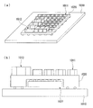
一方、キャビティ基板(部品内蔵基板)を用いた構成がある。図8は、キャビティ基板を用いた電子部品の実装構造を示す図である。図8(a)は、キャビティ基板を用いた電子部品の実装構造を示す斜視図である。図8(b)は、キャビティ基板を用いた電子部品の実装構造を示す断面図である。
図8に示すように、キャビティ基板を用いた電子部品の実装構造は、基体1010と、基体1010と対向して配置されたキャビティ基板1020と、キャビティ基板1020のキャビティ部に配置された能動素子1021と、キャビティ基板1020の上に配置された両端に電極を有する複数の受動素子1011,1012と、を備えた構造となっている。各受動素子1011,1012の両端の電極の双方は、キャビティ基板1020と接続されている。
On the other hand, there is a configuration using a cavity substrate (component built-in substrate). FIG. 8 is a view showing a mounting structure of an electronic component using a cavity substrate. FIG. 8A is a perspective view showing a mounting structure of an electronic component using a cavity substrate. FIG. 8B is a cross-sectional view showing a mounting structure of an electronic component using a cavity substrate.
As shown in FIG. 8, an electronic component mounting structure using a cavity substrate includes a
しかしながら、キャビティ基板を用いた構成では、能動素子と受動素子との間で配線抵抗が増加したりインダクタ成分の発生によりノイズが生じたりする等の問題がある。また、能動素子(電子部品)を基体とキャビティ基板の間におけるキャビティ部のみに配置する構成であるため、電子部品を高密度に配置するにも限界がある。 However, the configuration using the cavity substrate has problems such as an increase in wiring resistance between the active element and the passive element and noise due to the generation of an inductor component. Further, since the active element (electronic component) is arranged only in the cavity portion between the base and the cavity substrate, there is a limit to arranging the electronic components at high density.
本発明はこのような事情に鑑みてなされたものであって、電子部品を高密度に配置するとともに装置全体の小型化を図ることが可能な電子部品の実装構造及び電子機器を提供することを目的とする。 The present invention has been made in view of such circumstances, and it is an object of the present invention to provide an electronic component mounting structure and an electronic apparatus in which electronic components are arranged at high density and the entire apparatus can be reduced in size. Objective.
上記の課題を解決するため、本発明に係る電子部品の実装構造は、第1基体と、前記第1基体と対向して配置された第2基体と、前記第1基体と前記第2基体の間に配置された、両端に電極を有する複数の第1受動素子と、前記第2基体の前記第1受動素子が配置された側とは反対の側に配置された能動素子と、を備え、前記第1受動素子の両端の電極のうち一方の電極は、前記第1基体と接続されており、他方の電極は、前記第2基体と接続されるとともに前記能動素子と電気的に接続されていることを特徴とする。 In order to solve the above-described problem, an electronic component mounting structure according to the present invention includes a first base, a second base disposed opposite to the first base, the first base, and the second base. A plurality of first passive elements having electrodes at both ends disposed therebetween, and an active element disposed on a side of the second base opposite to the side on which the first passive elements are disposed, One of the electrodes at both ends of the first passive element is connected to the first base, and the other electrode is connected to the second base and electrically connected to the active element. It is characterized by being.
本発明に係る電子部品の実装構造は、基体と、前記基体と対向して配置された導電性のシールド部材と、前記基体と前記シールド部材の間に配置された、両端に電極を有する複数の受動素子と、前記基体の前記受動素子が配置された側とは反対の側に配置された能動素子と、を備え、前記シールド部材は、前記受動素子の両端の電極のうち一方の電極と対向する位置に開口部が形成された天井部と、前記受動素子の側方を覆う側壁部と、を備え、前記受動素子の一方の電極は、前記開口部に圧入された状態で前記シールド部材と接続されており、前記受動素子の他方の電極は、前記基体と接続されるとともに前記能動素子と電気的に接続されていることを特徴とする。 An electronic component mounting structure according to the present invention includes a base, a conductive shield member disposed to face the base, and a plurality of electrodes disposed between the base and the shield member, each having an electrode at both ends. A passive element and an active element disposed on a side of the substrate opposite to the side on which the passive element is disposed, and the shield member is opposed to one of the electrodes at both ends of the passive element. A side wall that covers the side of the passive element, and one electrode of the passive element is press-fitted into the opening and the shield member. The other electrode of the passive element is connected to the base and electrically connected to the active element.
本発明に係る電子機器は、上記電子部品の実装構造を備えることを特徴とする。 An electronic apparatus according to the present invention includes a mounting structure for the electronic component.
本発明によれば、電子部品を高密度に配置するとともに装置全体の小型化を図ることが可能となる。 According to the present invention, it is possible to arrange electronic components at high density and to reduce the size of the entire apparatus.
以下、図面を参照して、本発明の実施の形態について説明する。かかる実施の形態は、本発明の一態様を示すものであり、この発明を限定するものではなく、本発明の技術的思想の範囲内で任意に変更可能である。また、以下の図面においては、各構成をわかりやすくするために、実際の構造と各構造における縮尺や数等が異なっている。 Embodiments of the present invention will be described below with reference to the drawings. This embodiment shows one aspect of the present invention, and does not limit the present invention, and can be arbitrarily changed within the scope of the technical idea of the present invention. Moreover, in the following drawings, in order to make each structure easy to understand, an actual structure and a scale, a number, and the like in each structure are different.
(第1実施形態)
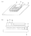
図1は、本発明の第1実施形態に係る電子部品の実装構造を示す図である。図1(a)は、本発明の第1実施形態に係る電子部品の実装構造を示す斜視図である。図1(b)は、本発明の第1実施形態に係る電子部品の実装構造を示す断面図である。
(First embodiment)
FIG. 1 is a diagram showing a mounting structure for an electronic component according to the first embodiment of the present invention. FIG. 1A is a perspective view showing a mounting structure for an electronic component according to the first embodiment of the present invention. FIG. 1B is a cross-sectional view showing the electronic component mounting structure according to the first embodiment of the present invention.
図1に示すように、本実施形態の電子部品の実装構造(電子機器)は、第1基体10と、第1基体10と対向して配置された第2基体20と、第1基体10と第2基体20の間に配置された、両端に電極11a,11bを有する複数の第1受動素子11と、第2基体20の第1受動素子11が配置された側とは反対の側に配置された能動素子21と、を備えた構造となっている。
As shown in FIG. 1, the electronic component mounting structure (electronic device) according to the present embodiment includes a
ここでは、第1基体10及び第2基体20としてプリント回路基板等の電子基板を挙げて説明する。なお、第1基体10及び第2基体20には、電子部品を実装するためのランドが設けられている。また、「受動素子」(受動部品)とは、エネルギーを消費または蓄積する機能をもった電子部品である。受動素子としては、例えば、コンデンサ、コイル、抵抗が挙げられる。「能動素子」(能動部品)とは、エネルギーを発生したり供給したり、あるいは増幅したり変換したりする機能をもった電子部品である。能動素子としては、例えば、IC、トランジスタ、ダイオードが挙げられる。
Here, an electronic board such as a printed circuit board will be described as the
第1受動素子11は、直方体形状をなし且つその長軸方向に沿う両端に電極11a,11bを有する。第1受動素子11の両端の電極11a,11bのうち一方の電極11aは、第1基体10と接続されている。他方の電極11bは、第2基体20と接続されるとともに能動素子21(裏面の端子)と電気的に接続されている。
The first
複数の第1受動素子11の長軸方向の長さは、互いに同じ長さになっている。つまり、複数の第1受動素子11の両端の電極11a,11b間の距離は、互いに同じ大きさになっている。
The plurality of first
第2基体20の能動素子21と対向する部分を除いた領域(第2基体20上の能動素子21が配置されていない領域)には、両端に電極12a,12bを有する複数の第2受動素子12が配置されている。第2受動素子12は、直方体形状をなし且つその長軸方向に沿う両端に電極12a,12bを有する。第2受動素子12の両端の電極12a,12bの双方は、第2基体20と接続されている。
A plurality of second passive
(電子部品の実装構造の製造方法)
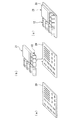
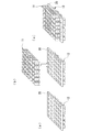
図2〜4は、本発明の第1実施形態に係る電子部品の実装構造(電子機器)の製造工程を示す図である。
(Method of manufacturing electronic component mounting structure)
2-4 is a figure which shows the manufacturing process of the mounting structure (electronic device) of the electronic component which concerns on 1st Embodiment of this invention.
先ず、第2基体20のパッドの上に、例えばスクリーン印刷機等の装置を用いて、クリーム半田(半田の粉末にフラックスを加えて、適当な粘度にしたもの)を印刷する(図2(a)参照)。 First, using a device such as a screen printer, for example, cream solder (a solder powder having a suitable viscosity by adding a flux) is printed on the pad of the second substrate 20 (FIG. 2A). )reference).
次に、第2基体20のクリーム半田が印刷された領域に、例えばチップマウンター等の設備を用いて、能動素子21及び第2受動素子12を搭載する(図2(b)参照)。
Next, the
次に、能動素子21及び第2受動素子12が搭載された第2基体20を適宜温度調整されたリフロー炉へ通し、リフロー半田付けを行う。これにより、能動素子21及び第2受動素子12と第2基体20とが接合される(図2(c)参照)。
Next, the
次に、能動素子21及び第2受動素子12が接合された第2基体20を反転し、反転した第2基体20のパッドの上に、例えばスクリーン印刷機等の装置を用いて、クリーム半田を印刷する(図3(a)参照)。
Next, the
次に、反転した第2基体20のクリーム半田が印刷された領域に、例えばチップマウンター等の設備を用いて、第1受動素子11を搭載する(図3(b)参照)。このとき、第1受動素子11の長軸方向は第2基体20の上面と直交する方向とする。また、複数の第1受動素子11の長軸方向の長さは、互いに同じ長さになっている。
Next, the 1st
次に、第1受動素子11が搭載された第2基体20を適宜温度調整されたリフロー炉へ通し、リフロー半田付けを行う。これにより、第1受動素子11(他方の電極11b)と第2基体20とが接合される(図3(c)参照)。
Next, the
次に、第1基体10のパッドの上に、例えばスクリーン印刷機等の装置を用いて、クリーム半田を印刷する(図4(a)参照)。
Next, cream solder is printed on the pad of the
次に、第1基体10のクリーム半田が印刷された領域に、例えばチップマウンター等の設備を用いて、第1受動素子11が搭載された第2基体20を搭載する(図4(b)参照)。
Next, the
次に、第2基体20が搭載された第1基体10を適宜温度調整されたリフロー炉へ通し、リフロー半田付けを行う。これにより、第1受動素子11(一方の電極11a)と第2基体20とが接合される(図4(c)参照)。このようにして、第1基体10と第2基体20とが第1受動素子11を介して電気的、機械的に接続される。
Next, the
なお、第1受動素子11の他方の電極11bは能動素子21(裏面の端子)と図示しない配線により電気的に接続される。本実施形態の電子部品の実装構造によれば、キャビティ基板を用いた構成に比べて、第1受動素子11と能動素子21との間に引き回される配線の長さを短くすることができる。このため、第1受動素子11と能動素子21との間で配線抵抗が増加することを抑制するとともにインダクタ成分の発生を抑えてノイズが生じることを抑制することができる。
The
以上の工程により、本実施形態に係る電子部品の実装構造を製造することができる。 Through the above steps, the electronic component mounting structure according to the present embodiment can be manufactured.
本実施形態の電子部品の実装構造によれば、第2基体20の両側に電子部品が配置される(第2基体20の一方の側に第1受動素子11が配置されるとともに他方の側に能動素子21が配置される)ので、特許文献1に示すように複数のチップ部品を一枚の実装基板上のみに配置する構成に比べて、電子部品が三次元的に配置されることとなる。したがって、電子部品を高密度に配置するとともに装置全体の小型化を図ることが可能となる。
According to the electronic component mounting structure of the present embodiment, electronic components are disposed on both sides of the second base 20 (the first
この構成によれば、第2基体20の能動素子21と対向する部分を除いた領域に第2受動素子12が配置されているので、第2基体の一方の側のみに受動素子が配置される構成に比べて、受動素子を高密度に配置することができる。
According to this configuration, since the second
この構成によれば、第1受動素子11が直方体形状をなし且つその長軸方向に沿う両端に電極11a,11bを有するので、第1受動素子11は起立した状態で第1基体10と第2基体20の間に実装されることとなる。このため、受動素子が基体に平行に実装する構成に比べて、第1受動素子11を起立状態に実装した分だけ実装密度を高めることができる。
According to this configuration, since the first
この構成によれば、複数の第1受動素子11の長軸方向の長さは、互いに同じ長さになっているので、第1基体10と第2基体20の間の距離が一定となる。このため、複数の第1受動素子の長軸方向の長さが互いに異なっている構成に比べて、第1受動素子11を第1基体10と第2基体20の間に安定して実装することができる。
According to this configuration, since the lengths in the major axis direction of the plurality of first
本実施形態の電子機器によれば、上述した電子部品の実装構造を備えているので、電子部品を高密度に配置するとともに装置全体の小型化を図ることが可能となる。 According to the electronic apparatus of the present embodiment, since the electronic component mounting structure described above is provided, the electronic components can be arranged at high density and the entire apparatus can be downsized.
(第2実施形態)
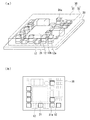
図5は、図1に対応した、本発明の第2実施形態に係る電子部品の実装構造を示す図である。図5(a)は、本発明の第1実施形態に係る電子部品の実装構造を示す斜視図である。図5(b)は、本発明の第1実施形態に係る電子部品の実装構造を示す断面図である。図5に示すように、本実施形態の電子部品の実装構造は、第2基体20の第1基体10(図示略)と対向する側と反対の側に導電性のシールド部材30が配置されている点で、上述の第1実施形態で説明した電子部品の実装構造と異なっている。その他の点は第1実施形態と同様であるので、図1と同様の要素には同一の符号を付し、詳細な説明は省略する。なお、図5においては、便宜上、第1基体10及び第1基体10と第2基体20の間に配置された第1受動素子11の図示を省略している。
(Second Embodiment)
FIG. 5 is a view showing a mounting structure of an electronic component according to the second embodiment of the present invention corresponding to FIG. FIG. 5A is a perspective view showing a mounting structure for an electronic component according to the first embodiment of the present invention. FIG. 5B is a cross-sectional view showing the electronic component mounting structure according to the first embodiment of the present invention. As shown in FIG. 5, in the electronic component mounting structure of the present embodiment, a
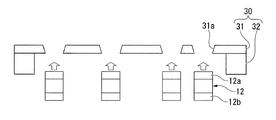
図5に示すように、第2基体20の第1基体10(図示略)と対向する側と反対の側に導電性のシールド部材30が配置されている。第2基体20とシールド部材30の間には、両端に電極12a,12bを有する複数の第2受動素子12及び能動素子21が配置されている。第2受動素子12は、直方体形状をなし且つその長軸方向に沿う両端に電極12a,12bを有する。第2受動素子12の両端の電極12a,12bのうち一方の電極12aは、シールド部材30と接続されている。他方の電極12bは、第2基体20と接続されている。
As shown in FIG. 5, a
例えば、シールド部材30にグラウンド電位をもたせ、第2受動素子12としてバイパスコンデンサ(電子回路において回路が動作する際に直流電源電圧が変動することを回避するために、電源ラインとグラウンドとを接続するコンデンサ)を用いることができる。
For example, a ground potential is applied to the
シールド部材30は、第2受動素子12の一方の電極12aと接続される天井部31と、第2受動素子12の側方を覆う側壁部32と、を備えている。シールド部材30の天井部31には、第2受動素子12の一方の電極12aと対向する位置に開口部31aが形成されている。第2受動素子12の一方の電極12aは、開口部31aに圧入された状態でシールド部材30と接続されている。
The
(電子部品の実装構造の製造方法)
図6は、本発明の第2実施形態に係る電子部品の実装構造(電子機器)の製造工程を示す図である。なお、図6においては、便宜上、第2基体20上に配置された第2受動素子12以外の部品の図示を省略している。また、第1受動素子11(一方の電極11a)と第2基体20とを接合する工程まで(図2〜図4参照)は、上述した第1実施形態に係る電子部品の実装構造の製造工程と同様であるため、その詳細な説明は省略する。
(Method of manufacturing electronic component mounting structure)
FIG. 6 is a diagram showing a manufacturing process of an electronic component mounting structure (electronic device) according to the second embodiment of the present invention. In FIG. 6, for the sake of convenience, illustration of components other than the second
図6に示すように、シールド部材30の天井部31には、第2受動素子12の一方の電極12aを挿通するための開口部31aが形成されている。複数の第2受動素子12の長軸方向の長さは、互いに同じ長さになっている。複数の第2受動素子12とシールド部材30との接続は、複数の第2受動素子12を開口部31aに圧入することにより行う。
As shown in FIG. 6, an opening 31 a for inserting one
開口部31aは、一方の電極12aの導入側(下側)の開口径が一方の電極12aの導出側(上側)の開口径よりも小さくなるように形成されている。このため、開口部31aの導入側(下側)から第2受動素子12(一方の電極12a)を圧入すると、開口部31aの下部が先鋭形状となっているため、一方の電極12aの表面の酸化膜が削られる。これにより、第2受動素子12とシールド部材30とが電気的に接続される。
The
以上の工程により、本実施形態に係る電子部品の実装構造を製造することができる。 Through the above steps, the electronic component mounting structure according to the present embodiment can be manufactured.
本実施形態の電子部品の実装構造によれば、シールド部材30の開口部31aに第2受動素子12が圧入された状態で接続されるので、隣接する第2受動素子12どうしのショートを抑制することが可能となる。
According to the electronic component mounting structure of the present embodiment, since the second
なお、本実施形態においては、第2基体20とシールド部材30の間に、複数の第2受動素子12及び能動素子21が配置されているが、これに限らない。例えば、第2基体とシールド部材の間に複数の第2受動素子のみが配置された構成であってもよい。
In the present embodiment, a plurality of second
(第3実施形態)
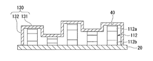
図7は、図5に対応した、本発明の第3実施形態に係る電子部品の実装構造を示す断面図である。図7に示すように、本実施形態の電子部品の実装構造は、受動素子112の一方の電極112aがシールド部材130の天井部131と導電部材40を介して接続されている点、第2基体20とシールド部材130の間に互いに異なる高さの受動素子112が配置されている点、で上述の第2実施形態で説明した電子部品の実装構造と異なっている。その他の点は第2実施形態と同様であるので、図2と同様の要素には同一の符号を付し、詳細な説明は省略する。なお、図7においては、便宜上、第1基体10及び第1基体10と第2基体20の間に配置された第1受動素子11の図示を省略している。
(Third embodiment)
FIG. 7 is a cross-sectional view showing an electronic component mounting structure according to the third embodiment of the present invention, corresponding to FIG. As shown in FIG. 7, the electronic component mounting structure of the present embodiment is characterized in that one
図7に示すように、受動素子112の一方の電極112aがシールド部材130と導電部材40を介して接続されている。例えば、導電部材40としては、異方性導電フィルム(ACF:anisotropic conductive film)や異方性導電ペースト(ACP:anisotropic conductive paste)を用いることができる。この場合、シールド部材130の天井部131に開口部を形成する必要はなく、ACFやACPを介して受動素子112(一方の電極112a)とシールド部材130(天井部131)とを熱圧着させることによって受動素子112とシールド部材130とが電気的、機械的に接続されることとなる。
As shown in FIG. 7, one
天井部131と側壁部132と第2基体20とに囲まれる空間には、相対的に長軸方向の長さの長い受動素子112(第3受動素子)と、相対的に長軸方向の長さの短い受動素子112(第4受動素子)と、が配置されている。第3受動素子112と対向する天井部131の第2基体20からの高さは、第4受動素子112と対向する天井部131の第2基体20からの高さよりも高くなっている。
In the space surrounded by the
本実施形態の電子部品の実装構造によれば、受動素子112の高さが互いに異なる場合であっても、各受動素子112とシールド部材130とを安定して接続することが可能となる。
According to the electronic component mounting structure of the present embodiment, each
なお、本実施形態においては、導電部材としてACFやACPを用いる構成を例に挙げて説明したが、これに限らない。例えば、導電部材としては、半田を用いることもできる。この場合、シールド部材の天井部に開口部を形成する必要はなく、天井部に半田めっきを施し、半田めっきを施した部分に受動素子を搭載してリフロー炉へ通すことによって受動素子とシールド部材とが電気的、機械的に接続されることとなる。 In the present embodiment, the configuration using ACF or ACP as the conductive member has been described as an example, but the present invention is not limited to this. For example, solder can be used as the conductive member. In this case, it is not necessary to form an opening in the ceiling part of the shield member, and the passive element and the shield member are formed by soldering the ceiling part, mounting the passive element on the soldered part, and passing it through a reflow furnace. Are electrically and mechanically connected.
10…第1基体、11…第1受動素子、11a…一方の電極、11b…他方の電極、20…第2基体、21…能動素子、30,130…シールド部材、31,131…天井部、31a…開口部、32,132…側壁部、40…導電部材、112…第3受動素子、第4受動素子
DESCRIPTION OF
Claims (10)
前記第1受動素子の両端の電極のうち一方の電極は、前記第1基体と接続されており、
他方の電極は、前記第2基体と接続されるとともに前記能動素子と電気的に接続されていることを特徴とする電子部品の実装構造。 A first base, a second base disposed opposite to the first base, a plurality of first passive elements having electrodes at both ends, disposed between the first base and the second base; An active element disposed on a side of the second base opposite to the side on which the first passive element is disposed,
One of the electrodes at both ends of the first passive element is connected to the first base,
The other electrode is connected to the second base and is electrically connected to the active element.
前記シールド部材は、
前記第2受動素子の一方の電極と接続される天井部と、
前記第2受動素子の側方を覆う側壁部と、
を備えていることを特徴とする請求項2に記載の電子部品の実装構造。 A conductive shield member is disposed on a side of the second base opposite to the side facing the first base,
The shield member is
A ceiling connected to one electrode of the second passive element;
A side wall covering a side of the second passive element;
The electronic component mounting structure according to claim 2, further comprising:
前記第2受動素子の一方の電極は、前記開口部に圧入された状態で前記シールド部材と接続されていることを特徴とする請求項5に記載の電子部品の実装構造。 An opening is formed in the ceiling of the shield member at a position facing one electrode of the second passive element,
6. The electronic component mounting structure according to claim 5, wherein one electrode of the second passive element is connected to the shield member while being press-fitted into the opening.
前記第3受動素子と対向する前記天井部の前記第2基体からの高さは、前記第4受動素子と対向する前記天井部の前記第2基体からの高さよりも高いことを特徴とする請求項5〜7のいずれか1項に記載の電子部品の実装構造。 A third passive element having a relatively long length in the long axis direction and a fourth having a relatively short length in the long axis direction are formed in a space surrounded by the ceiling portion, the side wall portion, and the second base. Passive elements are arranged,
The height of the ceiling part facing the third passive element from the second base is higher than the height of the ceiling part facing the fourth passive element from the second base. Item 8. The electronic component mounting structure according to any one of Items 5 to 7.
前記シールド部材は、前記受動素子の両端の電極のうち一方の電極と対向する位置に開口部が形成された天井部と、前記受動素子の側方を覆う側壁部と、を備え、
前記受動素子の一方の電極は、前記開口部に圧入された状態で前記シールド部材と接続されており、
前記受動素子の他方の電極は、前記基体と接続されるとともに前記能動素子と電気的に接続されていることを特徴とする電子部品の実装構造。 A base, a conductive shield member disposed opposite to the base, a plurality of passive elements having electrodes at both ends, disposed between the base and the shield member, and the passive elements of the base An active element disposed on a side opposite to the disposed side, and
The shield member includes a ceiling part in which an opening is formed at a position facing one of the electrodes at both ends of the passive element, and a side wall part that covers the side of the passive element,
One electrode of the passive element is connected to the shield member in a state of being press-fitted into the opening,
2. The electronic component mounting structure according to claim 1, wherein the other electrode of the passive element is connected to the base and electrically connected to the active element.
Priority Applications (1)
| Application Number | Priority Date | Filing Date | Title |
|---|---|---|---|
| JP2010228350A JP2012084635A (en) | 2010-10-08 | 2010-10-08 | Electronic component mounting structure and electronic device |
Applications Claiming Priority (1)
| Application Number | Priority Date | Filing Date | Title |
|---|---|---|---|
| JP2010228350A JP2012084635A (en) | 2010-10-08 | 2010-10-08 | Electronic component mounting structure and electronic device |
Publications (1)
| Publication Number | Publication Date |
|---|---|
| JP2012084635A true JP2012084635A (en) | 2012-04-26 |
Family
ID=46243227
Family Applications (1)
| Application Number | Title | Priority Date | Filing Date |
|---|---|---|---|
| JP2010228350A Pending JP2012084635A (en) | 2010-10-08 | 2010-10-08 | Electronic component mounting structure and electronic device |
Country Status (1)
| Country | Link |
|---|---|
| JP (1) | JP2012084635A (en) |
Cited By (1)
| Publication number | Priority date | Publication date | Assignee | Title |
|---|---|---|---|---|
| WO2018029921A1 (en) * | 2016-08-09 | 2018-02-15 | 株式会社村田製作所 | Semiconductor package and wiring board |
-
2010
- 2010-10-08 JP JP2010228350A patent/JP2012084635A/en active Pending
Cited By (1)
| Publication number | Priority date | Publication date | Assignee | Title |
|---|---|---|---|---|
| WO2018029921A1 (en) * | 2016-08-09 | 2018-02-15 | 株式会社村田製作所 | Semiconductor package and wiring board |
Similar Documents
| Publication | Publication Date | Title |
|---|---|---|
| KR100616384B1 (en) | Electronic assembly with vertically connected capacitors and manufacturing method | |
| US8064211B2 (en) | Passive component and electronic component module | |
| US10109576B2 (en) | Capacitor mounting structure | |
| JP2010129877A (en) | Electronic component module | |
| US8806420B2 (en) | In-grid on-device decoupling for BGA | |
| JP5920634B2 (en) | Printed board | |
| CN108307584A (en) | Component module | |
| JP5169800B2 (en) | Electronic equipment | |
| JP6121926B2 (en) | Semiconductor device and electronic apparatus using the same | |
| CN101867286A (en) | A DC/DC module power supply | |
| JP2002009229A (en) | Semiconductor device | |
| JP2013065887A (en) | Electronic device | |
| JP2011155199A (en) | Circuit mounting substrate | |
| JP4952365B2 (en) | Electronic component mounting structure on a double-sided mounting circuit board, semiconductor device, and manufacturing method of double-sided mounting semiconductor device | |
| JP2010045090A (en) | Assembling of electronic component on ic chip | |
| JP6587795B2 (en) | Circuit module | |
| JP5626892B2 (en) | Three-dimensional mounting type semiconductor device and electronic device | |
| CN111199934B (en) | Circuit device and circuit design and assembly method | |
| JP6264721B2 (en) | Multi-layer wiring board heat dissipation structure | |
| US20200152559A1 (en) | Device conducive to reduction of parasitic inductance and method for circuit design and assembly | |
| CN102969292B (en) | Integrated power supply module | |
| JP2008112941A (en) | Electronic component module | |
| JP4950581B2 (en) | Circuit module | |
| JP4985852B2 (en) | Mounted electronic circuit module | |
| JP4801603B2 (en) | Power module |