JP2012081663A - Transparent electrically conductive base material, and touch panel - Google Patents
Transparent electrically conductive base material, and touch panel Download PDFInfo
- Publication number
- JP2012081663A JP2012081663A JP2010230084A JP2010230084A JP2012081663A JP 2012081663 A JP2012081663 A JP 2012081663A JP 2010230084 A JP2010230084 A JP 2010230084A JP 2010230084 A JP2010230084 A JP 2010230084A JP 2012081663 A JP2012081663 A JP 2012081663A
- Authority
- JP
- Japan
- Prior art keywords
- transparent conductive
- transparent
- oxide
- compound
- conductive layer
- Prior art date
- Legal status (The legal status is an assumption and is not a legal conclusion. Google has not performed a legal analysis and makes no representation as to the accuracy of the status listed.)
- Pending
Links
Images

Landscapes
- Position Input By Displaying (AREA)
- Non-Insulated Conductors (AREA)
- Laminated Bodies (AREA)
Abstract
【課題】塗布法によるパターン透明導電層を有する透明導電基材におけるパターン透明導電層部分と、その開口部との相違を抑制した見栄えの良好な透明導電基材と、タッチパネルを提供する。
【解決手段】
透明基板上に塗布法で順次形成したパターン透明導電層、透明誘電体層の上に、透明樹脂層を備える透明導電基材であって、透明基板の屈折率1.46〜1.60、パターン透明導電層は有機金属化合物Aが主成分の塗布液を加熱処理し、有機金属化合物Aから得た導電性酸化物の微粒子層で、屈折率1.60〜1.75、膜厚100〜200nm、透明誘電体層は有機金属化合物Bが主成分の塗布液を加熱処理し、有機金属化合物Bから得た誘電性酸化物の微粒子層で、パターン透明導電層より屈折率が小さく、1.57〜1.65、膜厚50〜85nm、透明樹脂層が透明誘電体層よりも小さい屈折率で、1.48〜1.59、膜厚5〜500μmである透明導電基材。
【選択図】図9The present invention provides a transparent conductive base material having a good appearance in which a difference between a pattern transparent conductive layer portion in a transparent conductive base material having a patterned transparent conductive layer by a coating method and an opening thereof is suppressed, and a touch panel.
[Solution]
A transparent conductive substrate provided with a transparent resin layer on a transparent conductive layer, a transparent conductive layer, and a transparent conductive layer sequentially formed on the transparent substrate by a coating method, wherein the refractive index of the transparent substrate is 1.46 to 1.60, the pattern The transparent conductive layer is a conductive oxide fine particle layer obtained from the organometallic compound A by heat-treating the coating solution containing the organometallic compound A as a main component, and has a refractive index of 1.60 to 1.75 and a film thickness of 100 to 200 nm. The transparent dielectric layer is a fine particle layer of a dielectric oxide obtained from the organometallic compound B by heat-treating a coating solution containing the organometallic compound B as a main component, and has a refractive index smaller than that of the patterned transparent conductive layer. A transparent conductive substrate having a refractive index of ˜1.65, a thickness of 50 to 85 nm, and a transparent resin layer having a refractive index smaller than that of the transparent dielectric layer, 1.48 to 1.59 and a thickness of 5 to 500 μm.
[Selection] Figure 9
Description
本発明は、透明導電基材と、これを用いたタッチパネルに関するものである。 The present invention relates to a transparent conductive substrate and a touch panel using the same.
近年、液晶パネル等の表示画像に指やペンなどを用いて接触操作して、その接触位置を入力するタッチパネルが広く用いられている。
なかでも静電容量式タッチパネルは、マルチ入力(2点以上の同時位置入力)が可能という特徴を有しているため、従来の抵抗式タッチパネルに比べ、高機能タッチパネルとして普及が加速しつつある。この静電容量式タッチパネルは、指で触れた位置の静電容量変化を検出する方式であり、通常は、ガラス等の透明基板上にマトリックス状の透明導電層からなる第1パターン透明電極と第2パターン透明電極を設けた構造を有している。
2. Description of the Related Art In recent years, touch panels that use a finger or a pen to touch a display image on a liquid crystal panel or the like and input the touch position are widely used.
In particular, the capacitive touch panel has a feature that multi-input (two or more simultaneous position inputs) is possible, and therefore, the use of the capacitive touch panel is accelerating as a high-functional touch panel as compared with a conventional resistive touch panel. This capacitance type touch panel is a method for detecting a change in capacitance at a position touched by a finger. Usually, the first pattern transparent electrode made of a matrix-like transparent conductive layer on the transparent substrate such as glass and the first electrode It has a structure in which two patterns of transparent electrodes are provided.
この透明導電層の形成材料としては、従来から導電性酸化物である錫ドープ酸化インジウム(Indium Tin Oxide、以下、「ITO」と表記する場合がある)が使用されており、そのITOからなる透明導電層(ITO層と称す)の製造方法としては、真空蒸着法、スパッタリング法、化学蒸着法等の蒸着法(気相法)が広く適用されている。
ところで、静電容量式タッチパネルにおいて、蒸着法(気相法)で形成されたマトリックス状のパターン透明導電層(ITO電極)を、操作面側から見るとパターン透明導電層(ITO電極)が形成されている部分とそうでない部分が存在している。このため、パターン透明導電層(ITO電極)が形成された部分と、そうでない部分では、透明基板よりも屈折率の高いパターン透明導電層(ITO電極)に起因して、反射プロファイルや透過プロファイルに差が生じ、パターン透明導電層(ITO電極)が容易に視認されて、タッチパネルとしての商品価値を低下させるという問題があった。
As a material for forming the transparent conductive layer, conventionally, a tin-doped indium oxide (Indium Tin Oxide, hereinafter sometimes referred to as “ITO”), which is a conductive oxide, has been used. As a method for producing a conductive layer (referred to as an ITO layer), a vapor deposition method (vapor phase method) such as a vacuum vapor deposition method, a sputtering method, or a chemical vapor deposition method is widely applied.
By the way, in the capacitive touch panel, when the matrix pattern transparent conductive layer (ITO electrode) formed by the vapor deposition method (vapor phase method) is viewed from the operation surface side, the pattern transparent conductive layer (ITO electrode) is formed. There are parts that are and parts that are not. For this reason, in the portion where the pattern transparent conductive layer (ITO electrode) is formed and the portion where it is not, the reflection profile and transmission profile are caused by the pattern transparent conductive layer (ITO electrode) having a higher refractive index than the transparent substrate. There is a problem that a difference occurs, the pattern transparent conductive layer (ITO electrode) is easily visually recognized, and the commercial value as a touch panel is lowered.
そこで、この問題(パターン透明導電層の不可視化問題)を解決する方法として、蒸着法(気相法)で形成されたパターン透明導電層(ITO電極)と透明基板の間に、屈折率が透明導電層や透明基板と異なる少なくとも1層以上からなる下地層を形成して、パターン透明導電層(ITO電極)を視認しにくくする方法(特許文献1、2参照)、あるいは、透明基板、及びその透明基板上に形成されたパターン透明導電層(ITO電極)の上に、透明導電層と屈折率が同等の高屈折率のオーバーコート層を形成して、パターン透明導電層(ITO電極)を視認しにくくする方法(特許文献3参照)が既に提案されている。 Therefore, as a method of solving this problem (the problem of making the pattern transparent conductive layer invisible), the refractive index is transparent between the pattern transparent conductive layer (ITO electrode) formed by the vapor deposition method (vapor phase method) and the transparent substrate. A method of making a pattern transparent conductive layer (ITO electrode) difficult to visually recognize by forming a base layer composed of at least one layer different from a conductive layer or a transparent substrate, or a transparent substrate and its On the patterned transparent conductive layer (ITO electrode) formed on the transparent substrate, a high refractive index overcoat layer having the same refractive index as the transparent conductive layer is formed, and the patterned transparent conductive layer (ITO electrode) is visually recognized. A method for making this difficult (see Patent Document 3) has already been proposed.
しかしながら、蒸着法(気相法)で透明導電層(ITO層)を形成した場合には、透明性と導電性に優れた均一な透明導電層(ITO層)を基板上に形成することができるという特長がある一方で、これに使用する膜形成装置は真空容器をベースとするため非常に高価であり、また基板成膜毎に製造装置内の成分ガス圧を精密に制御しなければならず、更には、電極を構成するパターン透明導電層を得るために、フォトエッチング工程(フォトレジストの露光・現像、酸エッチング、レジスト剥離)を必要とするため、製造コストと量産性に問題があった。 However, when a transparent conductive layer (ITO layer) is formed by vapor deposition (gas phase method), a uniform transparent conductive layer (ITO layer) excellent in transparency and conductivity can be formed on the substrate. On the other hand, the film forming apparatus used for this is very expensive because it is based on a vacuum vessel, and the component gas pressure in the manufacturing apparatus must be precisely controlled each time a substrate is formed. Furthermore, since a photo-etching process (exposure / development of photoresist, acid etching, resist stripping) is required to obtain a patterned transparent conductive layer constituting an electrode, there are problems in manufacturing cost and mass productivity. .
一方、蒸着法(気相法)による透明導電層(ITO層)の問題を解決する製造方法として、インジウム化合物と錫化合物を溶剤に溶解させた透明導電層形成用塗布液を用いて、基板上に塗布する方法(以下、「塗布法」または「ウェットコーティング法」と表記する場合がある)が検討されてきた。
この基板上に塗布する方法では、透明導電層形成用塗布液の基板上へのパターン塗布、乾燥、焼成という簡素な製造工程でパターン透明導電層(ITO層)を形成するもので、その塗布液の基板上への塗布法には、インクジェット印刷法、スクリーン印刷法、グラビア印刷法、オフセット印刷法、フレキソ印刷法、ディスペンサ印刷法、スリットコート法、ダイコート法、スプレーコート法等が知られている。
On the other hand, as a manufacturing method for solving the problem of the transparent conductive layer (ITO layer) by the vapor deposition method (vapor phase method), a coating solution for forming a transparent conductive layer in which an indium compound and a tin compound are dissolved in a solvent is used. The method of applying to the surface (hereinafter sometimes referred to as “application method” or “wet coating method”) has been studied.
In this method of coating on the substrate, the pattern transparent conductive layer (ITO layer) is formed by a simple manufacturing process of pattern coating, drying, and firing on the substrate of the coating solution for forming the transparent conductive layer. As the coating method on the substrate, inkjet printing method, screen printing method, gravure printing method, offset printing method, flexographic printing method, dispenser printing method, slit coating method, die coating method, spray coating method and the like are known. .
このような塗布法に用いられる塗布液として、インジウム化合物及び錫化合物を含む塗布液が、従来種々開発されており、例えば、アセチルアセトンを配位した有機インジウム錯体と錫錯体からなる有機化合物混合溶液(特許文献4、特許文献5、特許文献6参照)が開示されている。
Various coating solutions containing an indium compound and a tin compound have been conventionally developed as a coating solution used in such a coating method. For example, an organic compound mixed solution composed of an organic indium complex coordinated with acetylacetone and a tin complex (
また、アセチルアセトンインジウム(正式名称:トリス(アセチルアセトナト)インジウム:In(C5H7O2)3)、アセチルアセトン錫(正式名称:ジ−n−ブトキシドビス(2,4−ペンタンジオナト)錫:[Sn(C4H9)2(C5H7O2)2])、ヒドロキシプロピルセルロース、アルキルフェノール及び/またはアルケニルフェノールと二塩基酸エステル及び/または酢酸ベンジルを含有する透明導電層形成用塗布液(特許文献7参照)が開示されており、この塗布液では、アセチルアセトンインジウム、アセチルアセトン錫の混合溶液にヒドロキシプロピルセルロースを含有させることによって塗布液の基板に対する濡れ性を改善すると同時に、粘性剤であるヒドロキシプロピルセルロースの含有量によって塗布液の粘度を調整し、スピンコート、スプレーコート、ディップコート、スクリーン印刷、ワイヤーバーコート等の各種塗布法が可能であり、パターン塗布により極めて簡便にパターン透明導電層(ITO層)を得ることができる。 Further, indium acetylacetonate (standard nomenclature: tris (acetylacetonato) indium: In (C 5 H 7 O 2) 3), acetylacetonate tin (official name: di -n- Butokishidobisu (2,4-pentanedionato) tin : [Sn (C 4 H 9 ) 2 (C 5 H 7 O 2) 2]), hydroxypropyl cellulose, a transparent conductive layer formed containing alkylphenols and / or alkenyl phenols and a dibasic acid ester and / or acetic acid benzyl A coating solution (see Patent Document 7) is disclosed. In this coating solution, the wettability of the coating solution to the substrate is improved by containing hydroxypropyl cellulose in a mixed solution of acetylacetone indium and acetylacetone tin, and at the same time, a viscous agent. Depending on the content of hydroxypropylcellulose By adjusting the viscosity of the coating solution, various coating methods such as spin coating, spray coating, dip coating, screen printing, and wire bar coating are possible. By pattern coating, a pattern transparent conductive layer (ITO layer) can be formed very easily. Obtainable.
しかしながら、上述の透明導電層形成用塗布液を用いて得られた透明導電層(ITO層)を、そのまま静電容量式タッチパネルのマトリックス状のパターン透明導電層(ITO電極)に適用した場合には、蒸着法(気相法)で形成されたパターン透明導電層(ITO電極)と同様に、パターン透明導電層(ITO電極)が容易に視認されるという問題があった。 However, when the transparent conductive layer (ITO layer) obtained using the above-described coating liquid for forming a transparent conductive layer is directly applied to the matrix-shaped pattern transparent conductive layer (ITO electrode) of the capacitive touch panel Similarly to the pattern transparent conductive layer (ITO electrode) formed by the vapor deposition method (vapor phase method), there is a problem that the pattern transparent conductive layer (ITO electrode) is easily visually recognized.
そこで、前述のアセチルアセトンインジウムとアセチルアセトン錫を含有する透明導電層形成用塗布液に、低屈折率透明微粒子を配合することによって、透明導電層の屈折率を低下させ、透明導電層の反射率を基板の反射率と同程度としてパターンの見えにくい低屈折率のパターン透明導電層を塗布法で得る方法も提案されている(特許文献8参照)。 Therefore, the refractive index of the transparent conductive layer is reduced by mixing the low refractive index transparent fine particles with the coating liquid for forming the transparent conductive layer containing indium acetylacetone and tin acetylacetone, and the reflectance of the transparent conductive layer is reduced to the substrate. A method has also been proposed in which a pattern transparent conductive layer having a low refractive index that is almost invisible with the same reflectivity as that of the above is obtained by a coating method (see Patent Document 8).
しかしながら、塗布法で得られる低屈折率のパターン透明導電層を、静電容量式タッチパネルのマトリックス状のパターン透明導電層(ITO電極)に適用した場合において、パターン透明導電層(ITO電極)が全く視認できない程の完全な不可視化を達成するためには、透明導電層形成用塗布液に低屈折率透明微粒子(例えばシリカ微粒子)を多量に配合してパターン透明導電層の屈折率を大幅に低下させる必要があり、その場合、透明導電層の抵抗値が悪化するため、必ずしも好ましいとは言えなかった。
従って、透明導電層形成用塗布液を用いたパターン塗布により、簡便にパターン透明導電層を形成できると同時に、パターン透明導電層の導電性に優れ、かつ、パターンが視認できない透明導電基材が要望されていた。
However, when the pattern transparent conductive layer having a low refractive index obtained by the coating method is applied to the matrix-shaped pattern transparent conductive layer (ITO electrode) of the capacitive touch panel, the pattern transparent conductive layer (ITO electrode) is not at all. In order to achieve complete invisibility that is not visible, a large amount of low refractive index transparent fine particles (for example, silica fine particles) are mixed in the coating liquid for forming the transparent conductive layer to greatly reduce the refractive index of the pattern transparent conductive layer. In this case, the resistance value of the transparent conductive layer is deteriorated, so that it is not necessarily preferable.
Therefore, there is a demand for a transparent conductive base material that can easily form a patterned transparent conductive layer by applying a pattern using a coating liquid for forming a transparent conductive layer, and at the same time has excellent conductivity of the patterned transparent conductive layer and the pattern is not visible. It had been.
本発明は、このような状況に鑑み、塗布法で形成されたパターン透明導電層を有する透明導電基材において、パターン透明導電層部分とパターン透明導電層の開口部との相違が抑制され、見栄えが良好で、かつ導電性に優れる透明導電基材と、これを用いたタッチパネルを提供することを目的とする。 In view of such a situation, the present invention has a transparent conductive substrate having a patterned transparent conductive layer formed by a coating method, and the difference between the pattern transparent conductive layer portion and the opening of the patterned transparent conductive layer is suppressed and looks good. An object of the present invention is to provide a transparent conductive substrate having good conductivity and excellent conductivity and a touch panel using the same.
このような課題に対し、発明者らは、透明導電層形成用塗布液を透明基板上にパターン塗布、乾燥、加熱処理して得られる透明基板上に形成されたパターン透明導電層について鋭意研究を重ねた結果、屈折率と膜厚が所定の範囲内に制御されたパターン透明導電層上に、そのパターン透明導電層よりも屈折率が小さく、且つ屈折率と膜厚が所定の範囲内に制御された透明誘電体層、更にその透明誘電体層上に、その透明誘電体層よりも屈折率が小さくかつ、屈折率と膜厚が所定の範囲内に制御された透明樹脂層を、順次形成すると、パターン透明導電層部分とパターン透明導電層の開口部の反射プロファイルの差異を極めて小さくすることが可能となり、パターン透明導電層(ITO電極)が全く視認できない透明導電基材が得られることを見出したものである。
更に、発明者らは、この透明導電基材を用いると極めて見栄えの良い静電容量式タッチパネルが得られることも見出し、本発明の完成に至ったものである。
In response to such problems, the inventors have conducted intensive research on a patterned transparent conductive layer formed on a transparent substrate obtained by applying a coating solution for forming a transparent conductive layer on a transparent substrate, drying, and heat treatment. As a result of overlapping, on the patterned transparent conductive layer whose refractive index and film thickness are controlled within a predetermined range, the refractive index is smaller than that of the patterned transparent conductive layer, and the refractive index and film thickness are controlled within a predetermined range. A transparent resin layer having a refractive index smaller than that of the transparent dielectric layer and having a refractive index and a film thickness controlled within a predetermined range is sequentially formed on the transparent dielectric layer. Then, the difference in the reflection profile between the pattern transparent conductive layer portion and the opening of the pattern transparent conductive layer can be made extremely small, and a transparent conductive base material in which the pattern transparent conductive layer (ITO electrode) cannot be seen at all can be obtained. It is those issued.
Furthermore, the inventors have found that a capacitive touch panel having a very good appearance can be obtained by using this transparent conductive substrate, and the present invention has been completed.
すなわち、本発明の第1の発明は、透明基板上に、塗布法で順次形成されたパターン透明導電層、透明誘電体層を有する無機積層基板の透明誘電体層上に、更に透明樹脂層を備える透明導電基材であって、その透明基板の屈折率が1.46〜1.60、パターン透明導電層は、有機金属化合物Aを主成分として含有する透明導電層形成用塗布液をパターン塗布、乾燥、加熱処理して、その有機金属化合物Aを燃焼または熱分解、あるいは燃焼および熱分解させて得られた導電性酸化物を主成分とするパターン導電性酸化物微粒子層で、その屈折率が1.60〜1.75、膜厚が100〜200nmであり、透明誘電体層は、有機金属化合物Bを主成分として含有する透明誘電体層形成用塗布液を塗布、乾燥、加熱処理して、その有機金属化合物Bを燃焼または熱分解、あるいは燃焼および熱分解させて得られた誘電性酸化物を主成分とする誘電性酸化物微粒子層で、その屈折率がパターン透明導電層の屈折率よりも小さく、その屈折率が1.57〜1.65、膜厚が50〜85nmであり、透明樹脂層は、その屈折率が透明誘電体層の屈折率よりも小さく、その屈折率は1.48〜1.59、膜厚が5〜500μmであることを特徴とする透明導電基材である。 That is, in the first invention of the present invention, a transparent resin layer is further formed on a transparent dielectric layer of an inorganic laminated substrate having a patterned transparent conductive layer and a transparent dielectric layer sequentially formed on the transparent substrate by a coating method. A transparent conductive substrate provided with a transparent substrate having a refractive index of 1.46 to 1.60, and the pattern transparent conductive layer is formed by applying a coating solution for forming a transparent conductive layer containing the organometallic compound A as a main component. A patterned conductive oxide fine particle layer mainly composed of a conductive oxide obtained by burning, pyrolysis, or combustion and pyrolysis of the organometallic compound A after drying, heat treatment, and its refractive index Is 1.60 to 1.75, the film thickness is 100 to 200 nm, and the transparent dielectric layer is formed by applying, drying, and heat-treating a coating liquid for forming a transparent dielectric layer containing the organometallic compound B as a main component. The organometallic compound A dielectric oxide fine particle layer mainly composed of a dielectric oxide obtained by burning or pyrolysis of B, or burning and pyrolysis, the refractive index of which is smaller than the refractive index of the patterned transparent conductive layer, The refractive index is 1.57-1.65, the film thickness is 50-85 nm, the transparent resin layer has a refractive index smaller than that of the transparent dielectric layer, and the refractive index is 1.48-1. 59, a transparent conductive substrate characterized in that the film thickness is 5 to 500 μm.
本発明の第2の発明は、第1の発明における透明樹脂層上に、更に第2の透明基板が設置され、その第2の透明基板の屈折率は1.46〜1.60、その透明樹脂層が透明接着剤層として、第2の透明基板と透明誘電体層とを接着していることを特徴とする透明導電基材である。 In the second invention of the present invention, a second transparent substrate is further provided on the transparent resin layer in the first invention, and the refractive index of the second transparent substrate is from 1.46 to 1.60. The transparent conductive base material is characterized in that the resin layer adheres the second transparent substrate and the transparent dielectric layer as a transparent adhesive layer.
本発明の第3の発明は、第1の発明における透明樹脂層上に更に第2の無機積層基板が設置され、その第2の無機積層基板は、第2の透明基板上に塗布法で順次形成された第2のパターン透明導電層、第2の透明誘電体層を有し、この第2のパターン透明導電層は、有機金属化合物Aを主成分として含有する透明導電層形成用塗布液をパターン塗布、乾燥、加熱処理し、その有機金属化合物Aを燃焼または熱分解、あるいは燃焼および熱分解させて得られた導電性酸化物を主成分とするパターン導電性酸化物微粒子層で、且つ屈折率が1.60〜1.75、その膜厚が100〜200nm、第2の透明誘電体層は、有機金属化合物Bを主成分として含有する透明誘電体層形成用塗布液を塗布、乾燥、加熱処理し、有機金属化合物Bを燃焼または熱分解、あるいは燃焼および熱分解させて得られた誘電性酸化物を主成分とする誘電性酸化物微粒子層で、且つ屈折率がパターン透明導電層の屈折率よりも小さく、その屈折率が1.57〜1.65、その膜厚が50〜85nmであり、透明樹脂層は、その屈折率が透明誘電体層及び第2の透明誘電体層のいずれの屈折率よりも小さく、且つ1.48〜1.59の屈折率を有して、その膜厚が5〜500μmであって、透明接着剤層として、第2の無機積層基板の第2の透明誘電体層と第1の透明誘電体層と接着していることを特徴とする透明導電基材である。 In the third invention of the present invention, a second inorganic laminated substrate is further installed on the transparent resin layer in the first invention, and the second inorganic laminated substrate is sequentially applied onto the second transparent substrate by a coating method. The formed second pattern transparent conductive layer and the second transparent dielectric layer have a transparent conductive layer forming coating solution containing the organometallic compound A as a main component. Pattern conductive oxide fine particle layer mainly composed of conductive oxide obtained by pattern coating, drying, heat treatment, combustion or thermal decomposition, or combustion and thermal decomposition of the organometallic compound A, and refraction The rate is 1.60 to 1.75, the film thickness is 100 to 200 nm, and the second transparent dielectric layer is coated with a coating liquid for forming a transparent dielectric layer containing the organometallic compound B as a main component, dried, Heat treatment to burn organometallic compound B or A dielectric oxide fine particle layer mainly composed of a dielectric oxide obtained by pyrolysis or combustion and pyrolysis, and the refractive index is smaller than the refractive index of the patterned transparent conductive layer, and the refractive index is 1. .57 to 1.65, the film thickness is 50 to 85 nm, and the transparent resin layer has a refractive index smaller than that of either the transparent dielectric layer or the second transparent dielectric layer, and 1. The film has a refractive index of 48 to 1.59 and a film thickness of 5 to 500 μm. The transparent adhesive layer includes a second transparent dielectric layer and a first transparent dielectric layer of the second inorganic laminated substrate. A transparent conductive substrate characterized by being bonded to a body layer.
本発明の第4の発明は、第1から第3の発明における有機金属化合物Aが、有機インジウム化合物、有機錫化合物、有機亜鉛化合物のいずれか一つ以上からなり、前記導電性酸化物が、酸化インジウム、酸化錫、酸化亜鉛のいずれか一つ以上であることを特徴とする透明導電基材である。 According to a fourth aspect of the present invention, the organometallic compound A in the first to third aspects comprises at least one of an organic indium compound, an organic tin compound, and an organic zinc compound, and the conductive oxide comprises: It is a transparent conductive substrate characterized by being one or more of indium oxide, tin oxide, and zinc oxide.
本発明の第5の発明は、第1から第3の発明における有機金属化合物Bが、有機アルミニウム化合物、有機ケイ素化合物、有機チタン化合物、有機ガリウム化合物、有機ゲルマニウム化合物、有機イットリウム化合物、有機ジルコニウム化合物、有機ニオブ化合物、有機モリブデン化合物、有機ハフニウム化合物、有機タンタル化合物、有機セリウム化合物のいずれか一つ以上からなり、前記誘電性酸化物が、酸化アルミニウム、二酸化ケイ素、酸化チタン、酸化ガリウム、酸化ゲルマニウム、酸化イットリウム、酸化ジルコニウム、酸化ニオブ、酸化モリブデン、酸化ハフニウム、酸化タンタル、酸化セリウムのいずれか一つ以上であることを特徴とする透明導電基材である。 According to a fifth aspect of the present invention, the organometallic compound B in the first to third aspects is an organoaluminum compound, organosilicon compound, organotitanium compound, organogallium compound, organogermanium compound, organoyttrium compound, organozirconium compound. , Organic niobium compound, organic molybdenum compound, organic hafnium compound, organic tantalum compound, organic cerium compound, and the dielectric oxide is aluminum oxide, silicon dioxide, titanium oxide, gallium oxide, germanium oxide A transparent conductive substrate characterized by being one or more of yttrium oxide, zirconium oxide, niobium oxide, molybdenum oxide, hafnium oxide, tantalum oxide, and cerium oxide.
本発明の第6の発明は、第1から第3の発明おける加熱処理が、露点温度−10℃以下の酸素含有雰囲気下で行い、少なくとも前記有機金属化合物Aの無機化が起こる温度または有機金属化合物Bの無機化が起こる温度以上まで昇温する加熱処理であることを特徴とする透明導電基材である。 According to a sixth aspect of the present invention, the heat treatment according to the first to third aspects is carried out in an oxygen-containing atmosphere having a dew point temperature of −10 ° C. or lower, and at least a temperature at which the organic metal compound A is mineralized or an organic metal A transparent conductive substrate characterized in that the heat treatment is performed to raise the temperature to a temperature at which compound B mineralization occurs or higher.
本発明の第7の発明は、第6の発明における加熱処理に続いて、中性雰囲気または還元性雰囲気下で加熱処理することを特徴とする透明導電基材である。 7th invention of this invention is a transparent conductive base material characterized by heat-processing in neutral atmosphere or reducing atmosphere following the heat processing in 6th invention.
本発明の第8の発明は、第7の発明における中性雰囲気が、窒素ガス、不活性ガスのいずれか一種以上、還元性雰囲気が、水素ガス若しくは前記中性雰囲気に水素ガス或いは有機溶剤蒸気の少なくとも一種以上が含まれた雰囲気であることを特徴とする透明導電基材である。 In an eighth aspect of the present invention, the neutral atmosphere in the seventh aspect is at least one of nitrogen gas and inert gas, the reducing atmosphere is hydrogen gas or hydrogen gas or organic solvent vapor in the neutral atmosphere. A transparent conductive substrate characterized in that the atmosphere contains at least one of the above.
本発明の第9の発明は、第6から第8の発明における露点温度−10℃以下の酸素含有雰囲気下で行われる加熱処理を施す際に、エネルギー線照射を行うことを特徴とする透明導電基材である。 According to a ninth aspect of the present invention, the transparent conductive material is characterized in that energy ray irradiation is performed when performing the heat treatment performed in an oxygen-containing atmosphere having a dew point temperature of −10 ° C. or lower in the sixth to eighth aspects. It is a substrate.
本発明の第10の発明は、第7、第8の発明における中性雰囲気または還元性雰囲気下の加熱処理を施す際に、エネルギー線照射を行うことを特徴とする透明導電基材である。 A tenth aspect of the present invention is a transparent conductive substrate characterized in that energy beam irradiation is performed when heat treatment is performed in a neutral atmosphere or a reducing atmosphere in the seventh and eighth aspects.
本発明の第11の発明は、第6の発明における露点温度−10℃以下の酸素含有雰囲気下で行われる加熱処理を施す際に、エネルギー線照射を行い、更に、引き続きプラズマ処理を施すことを特徴とする透明導電基材である。 In the eleventh aspect of the present invention, when heat treatment is performed in an oxygen-containing atmosphere having a dew point temperature of −10 ° C. or lower in the sixth aspect of the invention, energy beam irradiation is performed, and plasma treatment is subsequently performed. It is the transparent conductive base material characterized.
本発明の第12の発明は、第9から第11の発明におけるエネルギー線照射が、少なくとも200nm以下の波長を主要成分の一つとして含む紫外線の照射であることを特徴とする透明導電基材である。 A twelfth aspect of the present invention is a transparent conductive substrate characterized in that the energy beam irradiation in the ninth to eleventh aspects of the present invention is irradiation with ultraviolet rays containing at least a wavelength of 200 nm or less as one of the main components. is there.
本発明の第13の発明は、第12の発明における少なくとも200nm以下の波長を主要成分の一つとして含む紫外線の照射が、低圧水銀ランプ、アマルガムランプ、エキシマランプのいずれかから放射される紫外線の照射であることを特徴とする透明導電基材である。 In a thirteenth aspect of the present invention, the irradiation of ultraviolet rays containing at least a wavelength of 200 nm or less as one of the main components in the twelfth aspect is ultraviolet rays emitted from any one of a low-pressure mercury lamp, an amalgam lamp, and an excimer lamp. A transparent conductive substrate characterized by irradiation.
本発明の第14の発明は、第11の発明におけるプラズマ処理が、マイクロ波プラズマ処理または高周波プラズマ処理であることを特徴とする透明導電基材である。 A fourteenth aspect of the present invention is a transparent conductive substrate characterized in that the plasma treatment in the eleventh aspect is a microwave plasma treatment or a high-frequency plasma treatment.
本発明の第15の発明は、第1から第3の発明におけるパターン塗布、または塗布が、インクジェット印刷法、スクリーン印刷法、グラビア印刷法、オフセット印刷法、フレキソ印刷法、ディスペンサ印刷法、スリットコート法、ダイコート法、ドクターブレードコート法、ワイヤーバーコート法、スピンコート法、ディップコート法、スプレーコート法、ロールコート法のいずれかで行われることを特徴とする透明導電基材である。 In the fifteenth aspect of the present invention, the pattern coating or coating in the first to third aspects is performed by an ink jet printing method, a screen printing method, a gravure printing method, an offset printing method, a flexographic printing method, a dispenser printing method, or a slit coat. A transparent conductive substrate characterized in that it is carried out by any one of a method, a die coating method, a doctor blade coating method, a wire bar coating method, a spin coating method, a dip coating method, a spray coating method, and a roll coating method.
本発明の第16の発明は、第1から第3の発明における透明基板が、ガラス基板またはプラスチック基板であることを特徴とする透明導電基材である。 According to a sixteenth aspect of the present invention, there is provided the transparent conductive substrate according to the first to third aspects, wherein the transparent substrate is a glass substrate or a plastic substrate.
本発明の第17の発明は、第1〜16のいずれかの発明に記載の透明導電基材を備えていることを特徴とするタッチパネルである。 A seventeenth aspect of the present invention is a touch panel comprising the transparent conductive substrate according to any one of the first to sixteenth aspects.
本発明の第18の発明は、第17の発明におけるタッチパネルが、静電容量式タッチパネルであることを特徴とするものである。 According to an eighteenth aspect of the present invention, the touch panel according to the seventeenth aspect is a capacitive touch panel.
本発明の透明導電基材は、透明基板と、その透明基板上に塗布法で順次形成された、屈折率と膜厚が所定の範囲内に制御されたパターン透明導電層および、そのパターン透明導電層よりも屈折率が小さくかつ、屈折率と膜厚が所定の範囲内に制御された透明誘電体層を有する無機積層基板を具備し、更にその無機積層基板の透明誘電体層上に、その透明誘電体層よりも屈折率が小さくかつ、屈折率と膜厚が所定の範囲内に制御された透明樹脂層を備えているために、そのパターン透明導電層部分とパターン透明導電層の開口部の反射プロファイルの差異を極めて小さくすることが可能となり、見栄えが良好(所謂、パターンが全く視認できない状態)で、かつ優れた導電性を有している。
加えて、この透明導電基材を適用したタッチパネル(特に静電容量式タッチパネル)は、極めて見栄えが良く、かつ簡便な方法で安価に得られる。
The transparent conductive substrate of the present invention includes a transparent substrate, a pattern transparent conductive layer formed on the transparent substrate by a coating method in order, with a refractive index and a film thickness controlled within a predetermined range, and the pattern transparent conductive An inorganic laminated substrate having a transparent dielectric layer having a refractive index smaller than that of the layer and having a refractive index and a film thickness controlled within a predetermined range, and further on the transparent dielectric layer of the inorganic laminated substrate, Since it has a transparent resin layer whose refractive index is smaller than that of the transparent dielectric layer and whose refractive index and film thickness are controlled within a predetermined range, the pattern transparent conductive layer portion and the opening of the pattern transparent conductive layer The difference in the reflection profile can be made extremely small, the appearance is good (the so-called pattern cannot be seen at all), and the film has excellent conductivity.
In addition, a touch panel (particularly a capacitive touch panel) to which the transparent conductive substrate is applied is very attractive and can be obtained at a low cost by a simple method.
以下、本発明の実施形態について、図面を参照しながら説明する。
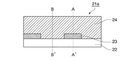
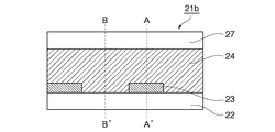
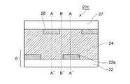
まず、図1、図2は従来のパターン透明導電層23を有する透明導電基材21a、21bを示す。
図1の透明導電基材21aは、透明基板22上に塗布法で形成されたパターン透明導電層23、更に透明基板22とパターン透明導電層23上に形成された透明樹脂層24で構成されている。
図2の透明導電基材21bは、図1の透明導電基材21aにおいて、第2の透明基板27が透明樹脂層24(透明接着剤層)を介して更に設けられているものである。第2の透明基板27には、例えばガラス基板等を用いることができ、この場合、第2の透明基板27は、パターン透明導電層23の抵抗値劣化(抵抗値の経時変化)や透明樹脂層24の傷付きなどを防止して、透明導電基材21bを保護する作用を有する。
Hereinafter, embodiments of the present invention will be described with reference to the drawings.
First, FIG. 1 and FIG. 2 show transparent
The transparent
The transparent
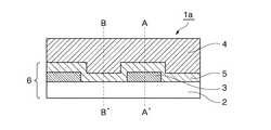
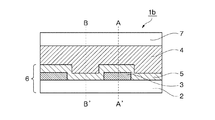
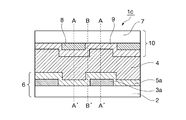
従来の透明導電基材に対して、図3、図4にパターン透明導電層3と透明誘電体層5を有する本発明の透明導電基材1a、1bを示す。
図3及び図4では、透明誘電体層5がパターン透明導電層3を覆うように塗布法で形成されており、この透明誘電体層5の存在により、パターン透明導電層部分とパターン透明導電層の開口部の反射プロファイルの差異が極めて小さく、パターン透明導電層3を全く視認できないようにすることを可能としている。
The transparent
3 and 4, the
後述するように、透明導電基材はタッチパネルに使用されるが、その際、パターン透明導電層3に接続する金属配線が形成されることとなる。したがって、透明誘電体層5は、必ずしも透明基板2の全面に形成する必要はなく、後述するタッチパネルの操作面に該当する部分の全面に形成されれば良い。したがって、一般的には、金属配線が形成される透明基板2の額縁部分(外周部分)には、透明誘電体層5を形成する必要はない。
なお、図4の本発明におけるパターン透明導電層3と透明誘電体層5を有する透明導電基材1bにおいて、第2の透明基板7が透明導電基材1bを保護する作用を有していることは、図2の場合と同様である。
As will be described later, the transparent conductive base material is used for the touch panel, and in this case, metal wiring connected to the pattern transparent
In addition, in the transparent
次に、各部材の材質、形状について説明する。
[透明基板]
本発明の透明基板としては、ソーダライムガラス、無アルカリガラス、石英ガラス等のガラス基板や、ポリエチレンナフタレート(PEN)、ポリエチレンテレフタレート(PET)、ナイロン、ポリエーテルスルホン(PES)、ウレタン、シクロオレフィン樹脂(例えば、ZEONOR:ゼオノア/商標:日本ゼオン株式会社製]やアートン:ARTON/商標:JSR株式会社製]等)、フッ素系樹脂、ポリイミド(PI)等の樹脂基板(所謂、耐熱性プラスチックフィルム)を用いることができる。
Next, the material and shape of each member will be described.
[Transparent substrate]
Examples of the transparent substrate of the present invention include glass substrates such as soda lime glass, non-alkali glass, and quartz glass, polyethylene naphthalate (PEN), polyethylene terephthalate (PET), nylon, polyethersulfone (PES), urethane, and cycloolefin. Resin substrates (for example, ZEONOR: ZEONOR / trademark: manufactured by ZEON Corporation) and ARTON: ARTON / trademark: manufactured by JSR Corporation), fluororesin, polyimide (PI), etc. (so-called heat-resistant plastic film) ) Can be used.
これら透明基板の屈折率は、1.46〜1.60であることが好ましく、耐熱性や透明性からすると、ガラス基板が良く、特にソーダライムガラス基板、無アルカリガラス基板が好ましい。尚、ソーダライムガラス基板として、その表面に圧縮応力層を形成して破壊強度を高めた強化ガラス(風冷強化ガラス、または化学強化ガラス)を用いることもできる。 The refractive index of these transparent substrates is preferably from 1.46 to 1.60. From the viewpoint of heat resistance and transparency, a glass substrate is preferable, and a soda lime glass substrate and an alkali-free glass substrate are particularly preferable. As the soda lime glass substrate, tempered glass (air-cooled tempered glass or chemically tempered glass) in which a compressive stress layer is formed on the surface thereof to increase the breaking strength can also be used.
透明基板の厚みは、基板の種類にもよるが、プラスチック基板(プラスチックフィルム)であれば25〜200μm、好ましくは50〜188μm、ガラス基板であれば、0.1〜1mm、好ましくは0.3〜0.7mmが良い。
基板の厚みが薄すぎると、撓みや割れ等のハンドリングの問題が生じ、逆に厚すぎると基板が重くなると同時にコストアップするので好ましくない。
透明基板は、パターン透明導電層3の抵抗値劣化(抵抗値の経時変化)や透明樹脂層4の傷付きなどを防止して、透明導電基材を保護する作用を有している。
The thickness of the transparent substrate depends on the type of the substrate, but is 25 to 200 μm, preferably 50 to 188 μm for a plastic substrate (plastic film), and 0.1 to 1 mm, preferably 0.3 for a glass substrate. ~ 0.7mm is good.
If the thickness of the substrate is too thin, handling problems such as bending and cracking occur. Conversely, if the thickness is too thick, the substrate becomes heavy and at the same time increases the cost.
The transparent substrate has a function of protecting the transparent conductive base material by preventing deterioration of the resistance value of the pattern transparent conductive layer 3 (change in resistance value with time) and scratching of the
[パターン透明導電層]
本発明のパターン透明導電層は、有機インジウム化合物、有機錫化合物、有機亜鉛化合物のいずれか一つ以上からなる有機金属化合物Aを主成分として含有する透明導電層形成用塗布液を、パターン塗布、乾燥、加熱処理して、有機金属化合物Aを燃焼または熱分解、あるいは燃焼および熱分解させて形成する、酸化インジウム、酸化錫、酸化亜鉛のいずれか一つ以上の導電性酸化物を主成分とするパターン導電性酸化物微粒子層で、且つ屈折率が1.60〜1.75、膜厚が100〜200nmであることが必要である。
[Pattern transparent conductive layer]
The pattern transparent conductive layer of the present invention comprises a coating solution for forming a transparent conductive layer containing, as a main component, an organometallic compound A composed of at least one of an organic indium compound, an organic tin compound, and an organic zinc compound, Mainly a conductive oxide of any one of indium oxide, tin oxide, and zinc oxide formed by drying or heat treatment to burn or pyrolyze organometallic compound A, or burn and pyrolyze And a patterned conductive oxide fine particle layer having a refractive index of 1.60 to 1.75 and a film thickness of 100 to 200 nm.
このパターン透明導電層の屈折率が1.60未満と低い場合には、パターン透明導電層上に透明誘電体層を形成しない従来の透明導電基材(図1;21a、図2:21bで示される)でも、パターン透明導電層の不可視化が可能となるからである。ただし、その場合には、前述した通り(特許文献8参照)、透明導電層形成用塗布液に低屈折率透明微粒子を多量に配合する必要があるため、透明導電層の抵抗値が悪化する場合があり、必ずしも好ましいとは言えない。 When the refractive index of this patterned transparent conductive layer is as low as less than 1.60, a conventional transparent conductive substrate that does not form a transparent dielectric layer on the patterned transparent conductive layer (shown in FIG. 1; 21a, FIG. 2: 21b) However, it is possible to make the patterned transparent conductive layer invisible. However, in that case, as described above (see Patent Document 8), it is necessary to blend a large amount of low refractive index transparent fine particles in the transparent conductive layer forming coating solution, and thus the resistance value of the transparent conductive layer is deteriorated. Therefore, it is not always preferable.
一方で、パターン透明導電層の屈折率が1.75を超えると、パターン透明導電層部分とパターン透明導電層の開口部の反射プロファイルの差異を極めて小さくすることが困難となり、パターン透明導電層が全く視認できない程の完全な不可視化を達成できなくなるからである。尚、塗布法で形成したパターン透明導電層は、導電性酸化物を主成分とする導電性酸化物微粒子層であって、層内に空隙を含有しているため、そもそもその屈折率が1.75を超える程に高めることは極めて難しい。 On the other hand, when the refractive index of the patterned transparent conductive layer exceeds 1.75, it becomes difficult to extremely reduce the difference in reflection profile between the patterned transparent conductive layer portion and the opening of the patterned transparent conductive layer. This is because complete invisibility that cannot be seen at all can be achieved. The pattern transparent conductive layer formed by the coating method is a conductive oxide fine particle layer containing a conductive oxide as a main component and contains voids in the layer. It is extremely difficult to increase it to more than 75.
[透明誘電体層]
本発明の透明誘電体層は、有機アルミニウム化合物、有機ケイ素化合物、有機チタン化合物、有機ガリウム化合物、有機ゲルマニウム化合物、有機イットリウム化合物、有機ジルコニウム化合物、有機ニオブ化合物、有機モリブデン化合物、有機ハフニウム化合物、有機タンタル化合物、有機セリウム化合物のいずれか一つ以上からなる有機金属化合物Bを主成分として含有する透明誘電体層形成用塗布液を塗布、乾燥、加熱処理して、有機金属化合物Bを燃焼または熱分解、あるいは燃焼および熱分解させて形成する、酸化アルミニウム(AlO1.5;屈折率=1.62)、二酸化ケイ素(SiO2;屈折率=1.46)、酸化チタン(TiO2;屈折率=2.5〜2.7)、酸化ガリウム(GaO1.5;屈折率=1.92)、酸化ゲルマニウム(GeO2:屈折率=1.99)、酸化イットリウム(YO1.5;屈折率=1.82)、酸化ジルコニウム(GeO2:屈折率=2.15)、酸化ニオブ(NbO2.5:屈折率=2.2〜2.3)、酸化モリブデン(MoO3;屈折率=1.85〜2.1)、酸化ハフニウム(HfO2:屈折率=1.91〜2.15)、酸化タンタル(TaO2.5;屈折率=2.16)、酸化セリウム(CeO2:屈折率=2.1〜2.5)のいずれか一つ以上の誘電性酸化物を主成分とする誘電性酸化物微粒子層であり、かつ、その屈折率が前記パターン透明導電層の屈折率よりも小さく、その屈折率は1.57〜1.65、膜厚は50〜85nmであることが必要である。
この条件範囲を外れると、パターン透明導電層部分とパターン透明導電層の開口部の反射プロファイルの差異を極めて小さくすることが困難となり、パターン透明導電層が全く視認できない程の完全な不可視化を達成できなくなるため、好ましくない。
[Transparent dielectric layer]
The transparent dielectric layer of the present invention comprises an organic aluminum compound, an organic silicon compound, an organic titanium compound, an organic gallium compound, an organic germanium compound, an organic yttrium compound, an organic zirconium compound, an organic niobium compound, an organic molybdenum compound, an organic hafnium compound, an organic A coating solution for forming a transparent dielectric layer containing as a main component an organometallic compound B composed of at least one of a tantalum compound and an organocerium compound is applied, dried, and heat-treated to burn or heat the organometallic compound B. Aluminum oxide (AlO 1.5 ; refractive index = 1.62), silicon dioxide (SiO 2 ; refractive index = 1.46), titanium oxide (TiO 2 ; refractive index) formed by decomposition or combustion and thermal decomposition = 2.5 to 2.7), gallium oxide (GaO 1.5; refractive index = 1.92), Germanium (GeO 2: refractive index = 1.99), yttrium oxide (YO 1.5; refractive index = 1.82), zirconium oxide (GeO 2: refractive index = 2.15), niobium oxide (NbO 2. 5: refractive index = 2.2 to 2.3), molybdenum oxide (MoO 3; refractive index = 1.85 to 2.1), hafnium oxide (HfO 2: refractive index = 1.91 to 2.15), Dielectric having a main component of one or more dielectric oxides of tantalum oxide (TaO 2.5 ; refractive index = 2.16) and cerium oxide (CeO 2 : refractive index = 2.1 to 2.5) And a refractive index of 1.57 to 1.65, and a film thickness of 50 to 85 nm. is there.
Outside this condition range, it becomes difficult to make the difference in reflection profile between the pattern transparent conductive layer and the opening of the pattern transparent conductive layer extremely small, and complete invisibility is achieved so that the pattern transparent conductive layer cannot be seen at all. Since it becomes impossible, it is not preferable.
[透明樹脂層(透明接着剤層)]
本発明の透明樹脂層は、その屈折率が透明誘電体層の屈折率よりも小さく、その屈折率は1.48〜1.59、膜厚は5〜500μm、好ましくは、10〜200μmであることが必要である。
透明樹脂層の屈折率が1.48〜1.59であるのは、安価で実用的な特性(耐久性、透明性、強度、密着性等)を有し、かつ一般的に得られる透明樹脂を用いるためである。
加えて、その屈折率範囲から大幅に外れると、パターン透明導電層部分とパターン透明導電層の開口部の反射プロファイルの差異を極めて小さくすることが困難となり、パターン透明導電層が全く視認できない程の完全な不可視化を達成できなくなるため、好ましくない。
[Transparent resin layer (transparent adhesive layer)]
The refractive index of the transparent resin layer of the present invention is smaller than the refractive index of the transparent dielectric layer, the refractive index is 1.48 to 1.59, the film thickness is 5 to 500 μm, preferably 10 to 200 μm. It is necessary.
The refractive index of the transparent resin layer is 1.48 to 1.59 because it is inexpensive and has practical properties (durability, transparency, strength, adhesion, etc.) and is generally obtained Is to use.
In addition, if the refractive index is significantly out of the refractive index range, it becomes difficult to make the difference in reflection profile between the pattern transparent conductive layer portion and the opening of the pattern transparent conductive layer extremely small, and the pattern transparent conductive layer cannot be seen at all. This is not preferable because complete invisibility cannot be achieved.
透明樹脂層の膜厚(厚み)を5〜500μmとするのは、5μm未満だと、均一に膜形成するのが困難になるのと同時に、膜厚の不均一に応じた干渉縞が発生しやすくなるからである。一方、500μmを越えても何ら利点がなく、逆に、透明導電基材、あるいはその透明導電基材を用いたタッチパネルの厚みが厚くなるため、好ましくない。 If the film thickness (thickness) of the transparent resin layer is set to 5 to 500 μm, if it is less than 5 μm, it becomes difficult to form a uniform film, and at the same time, interference fringes corresponding to non-uniform film thickness occur. This is because it becomes easier. On the other hand, even if it exceeds 500 μm, there is no advantage, and conversely, the thickness of the transparent conductive substrate or the touch panel using the transparent conductive substrate is not preferable.
[透明導電層形成用塗布液]
次に、本発明で用いられる透明導電層形成用塗布液について詳細する。
本発明では、有機インジウム化合物、有機錫化合物、有機亜鉛化合物のいずれか一つ以上の有機金属化合物Aを主成分とする透明導電層形成用塗布液を用いて、酸化インジウム、酸化錫、酸化亜鉛のいずれか一つ以上を主成分とする透明導電層を形成する。
一般に透明導電層の導電性は高い方が望ましく、そのような場合には、酸化インジウム、酸化錫、酸化亜鉛という主成分となる酸化物に、それ以外の金属化合物、主として金属酸化物をドーピングすることで導電性を向上させる。即ち、ドーパント金属化合物を含む酸化インジウム、酸化錫、酸化亜鉛を導電性酸化物として用いれば、透明導電層の導電性は向上する。
これは、導電性酸化物において、ドーパント金属化合物がキャリアとしての電子の濃度(キャリア密度)を高める働きがあるからである。
[Coating liquid for forming transparent conductive layer]
Next, the coating liquid for forming a transparent conductive layer used in the present invention will be described in detail.
In the present invention, an indium oxide, tin oxide, zinc oxide is used by using a coating liquid for forming a transparent conductive layer mainly composed of at least one of an organoindium compound, an organotin compound, and an organozinc compound. A transparent conductive layer containing at least one of the above as a main component is formed.
In general, it is desirable that the transparent conductive layer has a higher conductivity. In such a case, an oxide that is a main component of indium oxide, tin oxide, or zinc oxide is doped with another metal compound, mainly a metal oxide. This improves the conductivity. That is, if indium oxide, tin oxide, or zinc oxide containing a dopant metal compound is used as the conductive oxide, the conductivity of the transparent conductive layer is improved.
This is because in the conductive oxide, the dopant metal compound functions to increase the concentration of electrons as carriers (carrier density).
その具体的なドーピングの方法としては、有機インジウム化合物、有機錫化合物、有機亜鉛化合物のいずれか一つ以上の有機金属化合物Aを主成分とする透明導電層形成用塗布液に、ドーパント用有機金属化合物を所定量配合する方法がある。
まず、有機インジウム化合物を主成分とする透明導電層形成用塗布液について、以下に説明する。
As a specific doping method, an organic metal for dopant is added to a coating liquid for forming a transparent conductive layer containing as a main component one or more of an organic indium compound, an organic tin compound, and an organic zinc compound. There is a method of blending a predetermined amount of a compound.
First, a coating liquid for forming a transparent conductive layer containing an organic indium compound as a main component will be described below.
本発明で用いる有機インジウム化合物には、アセチルアセトンインジウム(正式名称:トリス(アセチルアセトナト)インジウム)[In(C5H7O2)3]、2−エチルヘキサン酸インジウム、蟻酸インジウム、インジウムアルコキシド等が挙げられるが、基本的には、溶剤に溶解し、加熱処理時、あるいはエネルギー線の照射併用した加熱処理時において塩素ガスや窒素酸化物ガスなどの有害ガスが発生せずに酸化物に分解する有機インジウム化合物であれば良い。これらの中でもアセチルアセトンインジウムは有機溶剤への溶解性が高く、単純な大気中加熱でも200〜250℃程度の温度で分解・燃焼(酸化)して酸化物となり、エネルギー線の照射(波長200nm以下の紫外線の照射)と併用すれば、上記温度よりも更に低温で分解・燃焼(酸化)して酸化物となるため好ましい。 The organic indium compound used in the present invention, indium acetylacetonate (standard nomenclature: tris (acetylacetonato) indium) [In (C 5 H 7 O 2) 3], 2- ethylhexanoate, indium formate, indium alkoxides Basically, it dissolves in a solvent and decomposes into an oxide without generating harmful gases such as chlorine gas and nitrogen oxide gas during heat treatment or heat treatment combined with energy ray irradiation. Any organic indium compound may be used. Among these, indium acetylacetone is highly soluble in organic solvents, and even when heated in the air, it decomposes and burns (oxidizes) at a temperature of about 200 to 250 ° C. to become an oxide, and is irradiated with energy rays (with a wavelength of 200 nm or less). When used in combination with UV irradiation, it is preferable because it decomposes and burns (oxidizes) at a temperature lower than the above temperature to form an oxide.
次に、導電性を向上させるドーパント用有機金属化合物としては、有機錫化合物、有機チタン化合物、有機ゲルマニウム化合物、有機亜鉛化合物、有機タングステン化合物、有機ジルコニウム化合物、有機タンタル化合物、有機ニオブ化合物、有機ハフニウム化合物、有機バナジウム化合物のいずれか一種以上が好ましい。
なお、透明導電層を適用するデバイスの種類(例えばタッチパネルの種類)によっては導電性がある程度低い(抵抗値が高い)ことが必要とされる場合もあるため、透明導電層形成用塗布液へのドーパント用有機金属化合物の添加は、必要に応じて適宜実施すればよい。
Next, as organometallic compounds for dopants that improve conductivity, organic tin compounds, organic titanium compounds, organic germanium compounds, organic zinc compounds, organic tungsten compounds, organic zirconium compounds, organic tantalum compounds, organic niobium compounds, organic hafnium Any one or more of a compound and an organic vanadium compound are preferable.
Depending on the type of device to which the transparent conductive layer is applied (for example, the type of touch panel), the conductivity may be required to be somewhat low (resistance value is high). What is necessary is just to implement suitably the addition of the organometallic compound for dopants as needed.
ドーパント用有機金属化合物の有機錫化合物(化合物中の錫の価数は2価、4価にこだわらない)としては、例えば、アセチルアセトン錫(正式名称:ジ−n−ブトキシド ビス(2,4−ペンタンジオナト)錫、[Sn(C4H9)2(C5H7O2)2]、オクチル酸錫、2−エチルヘキサン酸錫、酢酸錫(II)[Sn(CH3COO)2]、酢酸錫(IV)[Sn(CH3COO)4]、ジ−n−ブチル錫ジアセテート[Sn(C4H9)2(CH3COO)2] 、蟻酸錫、錫アルコキシドとしての錫−tert−ブトキシド[Sn(C4H9O)4]等が挙げられるが、基本的には、溶剤に溶解し、加熱処理時、あるいはエネルギー線の照射併用した加熱処理時において塩素ガスや窒素酸化物ガスなどの有害ガスが発生せずに酸化物に分解する有機錫化合物であれば良い。これらの中でも、アセチルアセトン錫は、比較的安価で入手し易いので好ましい。
Examples of the organotin compound as the organometallic compound for the dopant (the tin valence in the compound is not limited to divalent or tetravalent) include, for example, acetylacetone tin (formal name: di-n-butoxide bis (2,4-pentane) dionato) tin, [Sn (C 4 H 9 ) 2 (C 5 H 7 O 2) 2], tin octylate, tin 2-ethylhexanoate, tin acetate (II) [Sn (CH 3 COO) 2] , tin acetate (IV) [Sn (CH 3 COO) 4], di -n- butyl tin diacetate [Sn (C 4 H 9) 2 (
ドーパント用有機金属化合物の有機チタン化合物としては、チタンアセチルアセトン錯体としてのアセチルアセトンチタン(正式名称:チタンジ−n−ブトキシド ビス(2,4−ペンタンジオネート)[Ti(C4H9O)2(C5H7O2)2])、チタニル(IV)アセチルアセトネート[(C5H7O2)4TiO]、チタンジイソプロポキシド ビス(2,4−ペンタンジオネート)[C16H36O4Ti]等や、チタンアルコキシドとしてのチタンテトラエトキシド[Ti(C2H5O)4]、チタン(IV)−tert−ブトキシド[Ti(C4H9O)4]、チタンテトラ−n−ブトキシド[Ti(C4H9O)4]、チタンテトライソプロポキシド[Ti(C3H7O)4]等が挙げられるが、基本的には、溶剤に溶解し、加熱処理時、あるいはエネルギー線の照射併用した加熱処理時において塩素ガスや窒素酸化物ガスなどの有害ガスが発生せずに酸化物に分解する有機チタン化合物であれば良い。これらの中でも、アセチルアセトンチタン、チタンテトラ−n−ブトキシド、チタンテトライソプロポキシドは、安価で入手し易いので好ましい。 As the organotitanium compound of the organometallic compound for dopant, acetylacetone titanium (formal name: titanium di-n-butoxide bis (2,4-pentanedionate) [Ti (C 4 H 9 O) 2 (C 5 H 7 O 2) 2] ), titanyl (IV) acetylacetonate [(C 5 H 7 O 2 ) 4 TiO], titanium diisopropoxide bis (2,4-pentanedionate) [C 16 H 36 O 4 Ti] and the like, titanium tetraethoxide as titanium alkoxide [Ti (C 2 H 5 O) 4 ], titanium (IV) -tert-butoxide [Ti (C 4 H 9 O) 4 ], titanium tetra- n-butoxide [Ti (C 4 H 9 O) 4 ], titanium tetraisopropoxide [Ti (C 3 H 7 O) 4 ] and the like. However, organic titanium that dissolves in a solvent and decomposes into oxide without generating harmful gases such as chlorine gas or nitrogen oxide gas during heat treatment or heat treatment combined with energy ray irradiation. Any compound may be used. Among these, acetylacetone titanium, titanium tetra-n-butoxide, and titanium tetraisopropoxide are preferable because they are inexpensive and easily available.
ドーパント用有機金属化合物の有機ゲルマニウム化合物としては、ゲルマニウムアルコキシドとしてのゲルマニウムテトラエトキシド[Ge(C2H5O)4]、ゲルマニウムテトラ−n−ブトキシド[Ge(C4H9O)4]、ゲルマニウムテトライソプロポキシド[Ge(C3H7O)4]等や、β−カルボキシエチルゲルマニウムオキシド[(GeCH2CH2COOH)2O3]、テトラエチルゲルマニウム[Ge(C2H5)4]、テトラブチルゲルマニウム[Ge(C4H9)4]、トリブチルゲルマニウム[Ge(C4H9)3]等が挙げられるが、基本的には、溶剤に溶解し、加熱処理時、あるいはエネルギー線の照射併用した加熱処理時において塩素ガスや窒素酸化物ガスなどの有害ガスが発生せずに酸化物に分解する有機ゲルマニウム化合物であれば良い。これらの中でも、ゲルマニウムテトラエトキシド、ゲルマニウムテトラ−n−ブトキシド、ゲルマニウムテトライソプロポキシドは、比較的安価で入手し易いので好ましい。 As an organic germanium compound of the organometallic compound for dopant, germanium tetraethoxide [Ge (C 2 H 5 O) 4 ], germanium tetra-n-butoxide [Ge (C 4 H 9 O) 4 ] as germanium alkoxide, Germanium tetraisopropoxide [Ge (C 3 H 7 O) 4 ] and the like, β-carboxyethyl germanium oxide [(GeCH 2 CH 2 COOH) 2 O 3 ], tetraethyl germanium [Ge (C 2 H 5 ) 4 ] , Tetrabutyl germanium [Ge (C 4 H 9 ) 4 ], tributyl germanium [Ge (C 4 H 9 ) 3 ], and the like, which are basically dissolved in a solvent and subjected to heat treatment or energy rays. During the heat treatment combined with the irradiation of harmful gases such as chlorine gas and nitrogen oxide gas Any organic germanium compound that decomposes into an oxide without being generated may be used. Among these, germanium tetraethoxide, germanium tetra-n-butoxide, and germanium tetraisopropoxide are preferable because they are relatively inexpensive and easily available.
ドーパント用有機金属化合物の有機亜鉛化合物としては、例えば、亜鉛アセチルアセトン錯体としてのアセチルアセトン亜鉛(正式名称:亜鉛−2,4−ペンタンジオネート)[Zn(C5H7O2)2]、亜鉛−2,2,6,6−テトラメチル−3,5−ヘプタンジオネート[Zn(C11H19O2)2]等が挙げられるが、基本的には、溶剤に溶解し、加熱処理時、あるいはエネルギー線の照射併用した加熱処理時において塩素ガスや窒素酸化物ガスなどの有害ガスが発生せずに酸化物に分解する有機亜鉛化合物であれば良い。これらの中でも、アセチルアセトン亜鉛は、安価で入手し易いので好ましい。 The organic zinc compound of the dopant organometallic compound, for example, zinc acetylacetonate as a zinc acetylacetone complex (official name: Zinc 2,4-pentanedionate) [Zn (C 5 H 7 O 2) 2], zinc - 2,2,6,6-tetramethyl-3,5-heptanedionate [Zn (C 11 H 19 O 2 ) 2 ] and the like can be mentioned, but basically, it is dissolved in a solvent and subjected to heat treatment. Alternatively, any organic zinc compound that decomposes into an oxide without generating harmful gas such as chlorine gas or nitrogen oxide gas during heat treatment combined with energy ray irradiation may be used. Among these, zinc acetylacetone is preferable because it is inexpensive and easily available.
ドーパント用有機金属化合物の有機タングステン化合物としては、タングステンアルコキシドとしてのタングステン(V)エトキシド[W(C2H5O)5]、タングステン(VI)エトキシド[W(C2H5O)6]等が挙げられるが、基本的には、溶剤に溶解し、加熱処理時、あるいはエネルギー線の照射併用した加熱処理時において塩素ガスや窒素酸化物ガスなどの有害ガスが発生せずに酸化物に分解する有機タングステン化合物であれば良い。 As the organotungsten compound of the organometallic compound for dopant, tungsten (V) ethoxide [W (C 2 H 5 O) 5 ], tungsten (VI) ethoxide [W (C 2 H 5 O) 6 ], etc. as tungsten alkoxide Basically, it dissolves in a solvent and decomposes into an oxide without generating harmful gases such as chlorine gas and nitrogen oxide gas during heat treatment or heat treatment combined with energy ray irradiation. Any organic tungsten compound may be used.
ドーパント用有機金属化合物の有機ジルコニウム化合物としては、ジルコニウムアセチルアセトン錯体としてのジルコニウム ジ−n−ブトキシド ビス(2,4−ペンタンジオネート)[Zr(C4H9O)2(C5H7O2)2]、アセチルアセトンジルコニウム(ジルコニウム−2,4−ペンタンジオネート)[Zr(C5H7O2)4]、ジルコニウムアルコキシドとしてのジルコニウムエトキシド[Zr(C2H5O)4]、ジルコニウム−n−プロポキシド[Zr(C3H7O)4]、ジルコニウムイソプロポキシド[Zr(C3H7O)4]、ジルコニウム−n−ブトキシド[Zr(C4H9O)4]、ジルコニウム−tert−ブトキシド[Zr(C4H9O)4]、ジルコニウム−2−メチル−2−ブトキシド[Zr(C5H11O)4]、ジルコニウム−2−メトキシメチル−2−プロポキシド[Zr(C5H11O2)4]等が挙げられるが、基本的には、溶剤に溶解し、加熱処理時、あるいはエネルギー線の照射併用した加熱処理時において塩素ガスや窒素酸化物ガスなどの有害ガスが発生せずに酸化物に分解する有機ジルコニウム化合物であれば良い。これらの中でも、ジルコニウム−n−プロポキシド、ジルコニウム−n−ブトキシドは、比較的安価で入手し易いので好ましい。 The organic zirconium compound as the dopant organometallic compound, zirconium di -n- butoxide bis as zirconium acetylacetone complex (2,4-pentanedionate) [Zr (C 4 H 9 O) 2 (C 5 H 7 O 2 ) 2], zirconium acetylacetonate (zirconium-2,4-pentanedionate) [Zr (C 5 H 7 O 2) 4], zirconium ethoxide as zirconium alkoxide [Zr (C 2 H 5 O ) 4], zirconium -n- propoxide [Zr (C 3 H 7 O ) 4], zirconium isopropoxide [Zr (C 3 H 7 O ) 4], zirconium -n- butoxide [Zr (C 4 H 9 O ) 4], zirconium -tert- butoxide [Zr (C 4 H 9 O ) 4], zirconium 2- Chill-2-butoxide [Zr (C 5 H 11 O ) 4], zirconium-2-methoxymethyl-2-propoxide [Zr (C 5 H 11 O 2) 4] and others as mentioned, basically Any organic zirconium compound may be used as long as it is dissolved in a solvent and decomposes into an oxide without generating harmful gases such as chlorine gas and nitrogen oxide gas during heat treatment or heat treatment combined with energy ray irradiation. Among these, zirconium-n-propoxide and zirconium-n-butoxide are preferable because they are relatively inexpensive and easily available.
ドーパント用有機金属化合物の有機タンタル化合物としては、タンタルアセチルアセトン錯体としてのタンタル(V)テトラエトキシド−ペンタンジオネート)[Ta(C5H7O2)(OC2H5)4]、タンタルアルコキシドとしてのタンタルメトキシド[Ta(CH3O)5]、タンタルエトキシド[Ta(C2H5O)5]、タンタルイソプロポキシド[Ta(C3H7O)5]、タンタル−n−ブトキシド[Ta(C4H9O)5]、テトラエトキシアセチルアセトナトタンタル[Ta(C2H5O)4(C5H7O2)]等が挙げられるが、基本的には、溶剤に溶解し、加熱処理時、あるいはエネルギー線の照射併用した加熱処理時において塩素ガスや窒素酸化物ガスなどの有害ガスが発生せずに酸化物に分解する有機タンタル化合物であれば良い。 The organic tantalum compound as the dopant organometallic compound, a tantalum as tantalum acetylacetone complex (V) tetraethoxide - pentanedionate) [Ta (C 5 H 7 O 2) (OC 2 H 5) 4], tantalum alkoxide Tantalum methoxide [Ta (CH 3 O) 5 ], tantalum ethoxide [Ta (C 2 H 5 O) 5 ], tantalum isopropoxide [Ta (C 3 H 7 O) 5 ], tantalum-n— Examples thereof include butoxide [Ta (C 4 H 9 O) 5 ], tetraethoxyacetylacetonato tantalum [Ta (C 2 H 5 O) 4 (C 5 H 7 O 2 )], and the like. No toxic gas such as chlorine gas or nitrogen oxide gas is generated during heat treatment or heat treatment combined with energy ray irradiation. It may be a decomposed organic tantalum compound to the oxide.
ドーパント用有機金属化合物の有機ニオブ化合物としては、ニオブアルコキシドとしてのニオブエトキシド[Nb(C2H5O)5]、ニオブ−n−ブトキシド[Nb(C4H9O)5]等が挙げられるが、基本的には、溶剤に溶解し、加熱処理時、あるいはエネルギー線の照射併用した加熱処理時において塩素ガスや窒素酸化物ガスなどの有害ガスが発生せずに酸化物に分解する有機ニオブ化合物であれば良い。 Examples of the organic niobium compound as the dopant organometallic compound include niobium ethoxide [Nb (C 2 H 5 O) 5 ], niobium-n-butoxide [Nb (C 4 H 9 O) 5 ] and the like as the niobium alkoxide. Basically, it dissolves in a solvent and decomposes into an oxide without generating harmful gases such as chlorine gas and nitrogen oxide gas during heat treatment or heat treatment combined with energy ray irradiation. Any niobium compound may be used.
ドーパント用有機金属化合物の有機ハフニウム化合物としては、ハフニウムアセチルアセトン錯体としてのハフニウム ジ−n−ブトキシド ビス(2,4−ペンタンジオネート)[Hf(C4H9O)2(C5H7O2)2]、アセチルアセトンハフニウム(ハフニウム−2,4−ペンタンジオネート)[Hf(C5H7O2)4]、ハフニウムアルコキシドとしてのハフニウムエトキシド[Hf(C2H5O)4]、ハフニウム−n−ブトキシド[Hf(C4H9O)4]、ハフニウム−tert−ブトキシド[Hf(C4H9O)4]、ハフニウム(VI)イソプロポキシドモノイソプロピレート[Hf(C3H7O)4(C3H7OH)]等が挙げられるが、基本的には、溶剤に溶解し、加熱処理時、あるいはエネルギー線の照射併用した加熱処理時において塩素ガスや窒素酸化物ガスなどの有害ガスが発生せずに酸化物に分解する有機ハフニウム化合物であれば良い。これらの中でも、ハフニウム−n−ブトキシドは、比較的安価で入手し易いので好ましい。
As the organic hafnium compound of the organometallic compound for dopant, hafnium di-n-butoxide bis (2,4-pentanedionate) [Hf (C 4 H 9 O) 2 (C 5 H 7 O 2 as a hafnium acetylacetone complex). ) 2], acetylacetone hafnium (hafnium 2,4-pentanedionate) [Hf (C 5 H 7 O 2) 4], hafnium ethoxide as hafnium alkoxide [Hf (C 2 H 5 O ) 4], hafnium -n- butoxide [Hf (C 4 H 9 O ) 4], hafnium -tert- butoxide [Hf (C 4 H 9 O ) 4], hafnium (VI) isopropoxide mono isopropylate [
ドーパント用有機金属化合物の有機バナジウム化合物としては、バナジウムアセチルアセトン錯体としてのバナジウムオキサイドビス−2,4−ペンタンジオネート[VO(C5H7O2)2]、アセチルアセトンバナジウム(バナジウム−2,4−ペンタンジオネート)[V(C5H7O2)3]等が挙げられるが、基本的には、溶剤に溶解し、加熱処理時、あるいはエネルギー線の照射併用した加熱処理時において塩素ガスや窒素酸化物ガスなどの有害ガスが発生せずに酸化物に分解する有機バナジウム化合物であれば良い。 As an organic vanadium compound of the organometallic compound for the dopant, vanadium oxide bis-2,4-pentanedionate [VO (C 5 H 7 O 2 ) 2 ] as vanadium acetylacetone complex, acetylacetone vanadium (vanadium-2,4- Pentanedionate) [V (C 5 H 7 O 2 ) 3 ] and the like. Basically, it is dissolved in a solvent and is used for chlorine gas or the like during heat treatment or heat treatment combined with irradiation of energy rays. Any organic vanadium compound that decomposes into an oxide without generating harmful gas such as nitrogen oxide gas may be used.
次に、有機錫化合物を主成分とする透明導電層形成用塗布液についても説明する。
本発明で用いる有機錫化合物には、有機インジウム化合物を主成分とする透明導電層形成用塗布液の説明で述べた有機錫化合物を用いることができ、導電性を向上させるドーパント用有機金属化合物としては、有機インジウム化合物、有機アンチモン化合物、有機リン化合物のいずれか一種以上が好ましい。
Next, the coating liquid for forming a transparent conductive layer containing an organic tin compound as a main component will be described.
As the organotin compound used in the present invention, the organotin compound described in the description of the coating liquid for forming a transparent conductive layer containing an organic indium compound as a main component can be used. Is preferably at least one of an organic indium compound, an organic antimony compound, and an organic phosphorus compound.
ドーパント用有機金属化合物としての有機インジウム化合物には、先に有機インジウム化合物を主成分とする透明導電層形成用塗布液の説明で述べた有機インジウム化合物を用いれば良い。
ドーパント用有機金属化合物の有機アンチモン化合物としては、酢酸アンチモン(III)[Sb(CH3COO)3]、アンチモンアルコキシドとしてのアンチモン(III)エトキシド[Sb(C2H5O)3]、アンチモン(III)−n−ブトキシド[Sb(C4H9O)3]等が挙げられるが、基本的には、溶剤に溶解し、加熱処理時、あるいはエネルギー線の照射併用した加熱処理時において塩素ガスや窒素酸化物ガスなどの有害ガスが発生せずに酸化物に分解する有機アンチモン化合物であれば良い。
これらの中でも、アンチモン(III)−n−ブトキシドは、比較的安価で入手し易いので好ましい。
As the organic indium compound as the organometallic compound for dopant, the organic indium compound described above in the description of the coating liquid for forming a transparent conductive layer containing the organic indium compound as a main component may be used.
As an organic antimony compound of the organometallic compound for the dopant, antimony acetate (III) [Sb (CH 3 COO) 3 ], antimony (III) ethoxide as antimony alkoxide [Sb (C 2 H 5 O) 3 ], antimony ( III) -n-butoxide [Sb (C 4 H 9 O) 3 ] and the like, which are basically dissolved in a solvent and subjected to chlorine gas during heat treatment or heat treatment combined with energy ray irradiation. Or an organic antimony compound that decomposes into an oxide without generating harmful gases such as nitrogen oxide gas.
Among these, antimony (III) -n-butoxide is preferable because it is relatively inexpensive and easily available.
ドーパント用有機金属化合物の有機リン化合物としては、トリエチルフォスフェイト[PO(C2H5O)3]等が挙げられるが、基本的には、溶剤に溶解し、加熱処理時、あるいはエネルギー線の照射併用した加熱処理時において塩素ガスや窒素酸化物ガスなどの有害ガスが発生せずに酸化物に分解する有機リン化合物であれば良い。 Examples of the organophosphorus compound of the organometallic compound for the dopant include triethyl phosphate [PO (C 2 H 5 O) 3 ] and the like. Any organic phosphorus compound that decomposes into oxide without generating harmful gas such as chlorine gas or nitrogen oxide gas during the heat treatment combined with irradiation may be used.
更に、有機亜鉛化合物を主成分とする透明導電層形成用塗布液についても説明する。
本発明で用いる有機亜鉛化合物には、有機インジウム化合物を主成分とする透明導電層形成用塗布液の説明で述べた有機亜鉛化合物を用いることができ、導電性を向上させるドーパント用有機金属化合物としては、有機アルミニウム化合物、有機インジウム化合物、有機ガリウム化合物のいずれか一種以上が好ましい。
Furthermore, the coating liquid for forming a transparent conductive layer containing an organic zinc compound as a main component will be described.
As the organic zinc compound used in the present invention, the organic zinc compound described in the explanation of the coating liquid for forming a transparent conductive layer containing an organic indium compound as a main component can be used. Is preferably at least one of an organic aluminum compound, an organic indium compound, and an organic gallium compound.
ドーパント用有機金属化合物としての有機インジウム化合物には、先に有機インジウム化合物を主成分とする透明導電層形成用塗布液の説明で述べた有機インジウム化合物を用いれば良い。 As the organic indium compound as the organometallic compound for dopant, the organic indium compound described above in the description of the coating liquid for forming a transparent conductive layer containing the organic indium compound as a main component may be used.
ドーパント用有機金属化合物の有機アルミニウム化合物としては、アルミニウムアセチルアセトン錯体としてのアセチルアセトンアルミニウム(アルミニウム−2,4−ペンタンジオネート)[Al(C5H7O2)3]、アルミニウムアルコキシドとしてのアルミニウムエトキシド[Al(C2H5O)3]、アルミニウム−n−ブトキシド[Al(C4H9O)3]、アルミニウム−tert−ブトキシド[Al(C4H9O)3]、アルミニウムイソプロポキシド[Al(C3H7O)3]等が挙げられるが、基本的には、溶剤に溶解し、加熱処理時、あるいはエネルギー線の照射併用した加熱処理時において塩素ガスや窒素酸化物ガスなどの有害ガスが発生せずに酸化物に分解する有機アルミニウム化合物であれば良い。これらの中でも、アセチルアセトンアルミニウム、アルミニウム−n−ブトキシドは、比較的安価で入手し易いので好ましい。 As the organoaluminum compound of the organometallic compound for the dopant, acetylacetone aluminum (aluminum-2,4-pentanedionate) [Al (C 5 H 7 O 2 ) 3 ] as an aluminum acetylacetone complex, aluminum ethoxide as an aluminum alkoxide [Al (C 2 H 5 O ) 3], aluminum -n- butoxide [Al (C 4 H 9 O ) 3], aluminum -tert- butoxide [Al (C 4 H 9 O ) 3], aluminum isopropoxide [Al (C 3 H 7 O) 3 ] and the like can be mentioned. Basically, chlorine gas, nitrogen oxide gas, etc. are dissolved in a solvent and subjected to heat treatment or heat treatment combined with energy ray irradiation. An organoaluminum compound that decomposes into oxides without the generation of harmful gases It may be Re. Among these, acetylacetone aluminum and aluminum-n-butoxide are preferable because they are relatively inexpensive and easily available.
ドーパント用有機金属化合物の有機ガリウム化合物としては、ガリウムアセチルアセトン錯体としてのアセチルアセトンガリウム(ガリウム−2,4−ペンタンジオネート)[Ga(C5H7O2)3]、ガリウムアルコキシドとしてのガリウムエトキシド[Ga(C2H5O)3]等が挙げられるが、基本的には、溶剤に溶解し、加熱処理時、あるいはエネルギー線の照射併用した加熱処理時において塩素ガスや窒素酸化物ガスなどの有害ガスが発生せずに酸化物に分解する有機ガリウム化合物であれば良い。 Examples of the organic gallium compound of the organometallic compound for the dopant include acetylacetone gallium (gallium-2,4-pentanedionate) [Ga (C 5 H 7 O 2 ) 3 ] as a gallium acetylacetone complex, and gallium ethoxide as a gallium alkoxide. [Ga (C 2 H 5 O) 3 ] and the like can be mentioned. Basically, chlorine gas, nitrogen oxide gas, etc. are dissolved in a solvent and subjected to heat treatment or heat treatment combined with energy ray irradiation. Any organic gallium compound that decomposes into an oxide without generating harmful gases may be used.
透明導電層形成用塗布液における有機インジウム化合物、有機錫化合物、有機亜鉛化合物のいずれか一つ以上の有機金属化合物A、または、この有機金属化合物Aとドーパント用有機金属化合物は、基板上に透明導電層を形成させるための主たる化合物原料であり、その合計含有量は1〜30重量%の範囲であることが好ましく、更に好ましくは5〜20重量%とするのが良い。
その合計含有量が1重量%未満であると膜厚の薄い透明導電層しか得られなくなるため十分な導電性が得られない。また、30重量%より多いと透明導電層形成用塗布液中の有機金属化合物Aが析出し易くなって塗布液の安定性が低下したり、得られる透明導電層が厚くなり過ぎて亀裂(クラック)が発生して導電性が損なわれる場合がある。
One or more organometallic compounds A of the organic indium compound, organotin compound, and organozinc compound in the coating solution for forming the transparent conductive layer, or the organometallic compound A and the organometallic compound for dopant are transparent on the substrate. It is a main compound raw material for forming the conductive layer, and the total content thereof is preferably in the range of 1 to 30% by weight, more preferably 5 to 20% by weight.
If the total content is less than 1% by weight, only a thin transparent conductive layer can be obtained, and sufficient conductivity cannot be obtained. On the other hand, if it exceeds 30% by weight, the organometallic compound A in the coating liquid for forming the transparent conductive layer is liable to precipitate and the stability of the coating liquid decreases, or the resulting transparent conductive layer becomes too thick and cracks (cracks) ) May occur and conductivity may be impaired.
また、透明導電層形成用塗布液にドーパント用有機金属化合物を配合する場合(高い導電性を得ようとする場合)には、有機金属化合物Aとド−パント用有機金属化合物の含有割合は、有機金属化合物A:ドーパント用有機金属化合物のモル比換算で99.9:0.1〜66.7:33.3が好ましい。詳しくは、有機インジウム化合物を主成分とする透明導電層形成用塗布液においてドーパント用有機金属化合物として有機亜鉛化合物を用いる場合を除いて、有機金属化合物:ドーパント用有機金属化合物のモル比換算で99.9:0.1〜87:13が良く、好ましくは99:1〜91:9である。 Moreover, when mix | blending the organometallic compound for dopants with the coating liquid for transparent conductive layer formation (when trying to obtain high electroconductivity), the content rate of the organometallic compound A and the organometallic compound for dopants is as follows. 99.9: 0.1-66.7: 33.3 is preferable in terms of molar ratio of organometallic compound A: organometallic compound for dopant. Specifically, except for the case where an organic zinc compound is used as the dopant organometallic compound in the coating liquid for forming a transparent conductive layer containing an organic indium compound as a main component, it is 99 in terms of a molar ratio of organometallic compound: organic metal compound for dopant. .9: 0.1-87: 13 is preferred, preferably 99: 1-91: 9.
なお、有機インジウム化合物を主成分とする透明導電層形成用塗布液において、有機亜鉛化合物をドーピング用有機金属化合物して用いる場合には、有機金属化合物A:ドーパント用有機金属化合物のモル比換算で95:5〜66.7:33.3が良く、好ましくは91:9〜71:29である。
ただし、透明導電層形成用塗布液におけるドーパント用有機金属化合物の配合割合は、マイクロ波プラズマ処理工程の基板加熱温度等の処理条件によっても、その適合範囲が変わってくるため、適用する工程条件によって上記記載範囲内で更に適宜最適化すると良い。
In addition, in the coating liquid for forming a transparent conductive layer containing an organic indium compound as a main component, when an organic zinc compound is used as an organometallic compound for doping, it is converted into a molar ratio of organometallic compound A: organometallic compound for dopant. 95: 5 to 66.7: 33.3 is good, and preferably 91: 9 to 71:29.
However, the blending ratio of the organometallic compound for the dopant in the coating liquid for forming the transparent conductive layer varies depending on the processing conditions such as the substrate heating temperature in the microwave plasma processing step, so the applicable range varies. It is better to further optimize within the above described range.
このモル比範囲を外れてド−パント用有機金属化合物が少なくても、或いは、多すぎても、透明導電層のキャリア密度が減少して透明導電層の導電性が急激に悪化する場合があり、また、上記モル比範囲を外れてド−パント用有機金属化合物が多い場合には、導電性酸化物微粒子の結晶成長が進みにくくなって導電性が悪化する場合があるため好ましくない。 Even if there is little or too much organometallic compound for dopants outside this molar ratio range, the carrier density of the transparent conductive layer may decrease and the conductivity of the transparent conductive layer may deteriorate rapidly. Moreover, when there are many dopant organometallic compounds outside the above molar ratio range, the crystal growth of the conductive oxide fine particles is difficult to proceed and the conductivity may be deteriorated.
さらに、透明導電層形成用塗布液には、有機バインダーを添加することが好ましい。
このバインダーを加えることで、基板に対する濡れ性が改善されると同時に、塗布液の粘度調整を行うことができる。添加するバインダーは加熱処理時、あるいはエネルギー線の照射併用した加熱処理時において燃焼や分解する材料が好ましく、このような材料として、セルロース誘導体、アクリル樹脂等が有効である。
Furthermore, it is preferable to add an organic binder to the coating liquid for forming a transparent conductive layer.
By adding this binder, the wettability to the substrate is improved, and at the same time, the viscosity of the coating solution can be adjusted. The binder to be added is preferably a material that burns or decomposes during heat treatment or heat treatment combined with irradiation of energy rays. As such a material, a cellulose derivative, an acrylic resin, or the like is effective.
有機バインダーに用いるセルロース誘導体としては、メチルセルロース、エチルセルロース、ヒドロキシメチルセルロース、ヒドロキシエチルセルロース 、ヒドロキシプロピルセルロース、ヒドロキシエチルメチルセルロース 、ヒドロキシプロピルメチルセルロース、エチルヒドロキシエチルセルロース、カルボキシメチルセルロース 、カルボキシエチルセルロース、カルボキシエチルメチルセルロース、ニトロセルロース等が挙げられるが、これらの中でもヒドロキシプロピルセルロース(以下、「HPC」と表記する場合がある)が好ましい。 Examples of the cellulose derivative used in the organic binder include methyl cellulose, ethyl cellulose, hydroxymethyl cellulose, hydroxyethyl cellulose, hydroxypropyl cellulose, hydroxyethyl methyl cellulose, hydroxypropyl methyl cellulose, ethyl hydroxyethyl cellulose, carboxymethyl cellulose, carboxyethyl cellulose, carboxyethyl methyl cellulose, nitrocellulose, and the like. Among these, hydroxypropylcellulose (hereinafter sometimes referred to as “HPC”) is preferable.
このHPCを用いれば、5重量%以下の含有量で十分な濡れ性が得られると同時に、大幅な粘度調整を行うことができる。またHPCの燃焼開始温度は単純な大気中加熱だと300℃程度だが、エネルギー線照射(例えば、波長200nm以下の紫外線照射)と併用すれば300℃未満の加熱温度でも分解・燃焼するので、生成する導電性粒子の粒成長を阻害せず、導電性が良好な透明導電層を作製することができる。
HPCの含有量が5重量%より多くなると、ゲル状になって塗布液中に残留し易くなり、極めて多孔質の透明導電層を形成して透明性や導電性が著しく損なわれる。
If this HPC is used, sufficient wettability can be obtained at a content of 5% by weight or less, and at the same time, the viscosity can be greatly adjusted. The combustion start temperature of HPC is about 300 ° C when heating in the air is simple, but it decomposes and burns even at heating temperatures below 300 ° C when used in combination with energy beam irradiation (for example, UV irradiation with a wavelength of 200 nm or less). Thus, it is possible to produce a transparent conductive layer having good conductivity without hindering the grain growth of the conductive particles.
When the content of HPC is more than 5% by weight, it becomes a gel and tends to remain in the coating solution, forming a very porous transparent conductive layer, and the transparency and conductivity are significantly impaired.
ここで、セルロース誘導体として、HPCの代わりにエチルセルロースを用いる場合には、HPCを用いる場合よりも塗布液の粘度が低く設定できるが、高粘度塗布液が好適であるスクリーン印刷法等ではパターン印刷性が若干低下する。
ところで、ニトロセルロースは、分解性は優れているが、加熱エネルギー線照射時やプラズマ処理時、あるいはその後の加熱処理時において有害な窒素酸化物ガスの発生があり、加熱処理炉の劣化や排ガス処理に問題を生じる場合がある。以上のように、使用するセルロース誘導体は、状況に応じて適宜選択する。
また、アクリル樹脂としては、比較的低温で燃焼するアクリル樹脂が好ましい。
Here, when ethyl cellulose is used as the cellulose derivative instead of HPC, the viscosity of the coating solution can be set lower than when HPC is used. However, in the case of a screen printing method or the like in which a high viscosity coating solution is suitable, pattern printability Decreases slightly.
By the way, although nitrocellulose is excellent in decomposability, harmful nitrogen oxide gas is generated at the time of heating energy ray irradiation, plasma treatment, or subsequent heat treatment, which causes deterioration of the heat treatment furnace and exhaust gas treatment. May cause problems. As described above, the cellulose derivative to be used is appropriately selected according to the situation.
The acrylic resin is preferably an acrylic resin that burns at a relatively low temperature.
更に、透明導電層形成用塗布液に、低屈折率透明微粒子を配合して、得られる透明導電層の屈折率を低下させてもよい。適用可能な低屈折率透明微粒子としては、屈折率1.5以下の物質(材料)からなる透明微粒子であって、例えば、酸化ケイ素微粒子(屈折率:1.46)、中空酸化ケイ素微粒子(屈折率:約1.3)、多孔質酸化ケイ素微粒子、フッ化マグネシウム微粒子(屈折率:1.38〜1.4)等が挙げられる。ただし、前述した通り、低屈折率透明微粒子の配合量が多くなると、得られる透明導電層において、その屈折率は大幅に低下できるが、同時に抵抗値が上昇するため、その屈折率が1.60以上となる程度に低屈折率透明微粒子の配合量を制限する。 Furthermore, you may mix | blend a low refractive index transparent microparticles | fine-particles with the coating liquid for transparent conductive layer formation, and may reduce the refractive index of the transparent conductive layer obtained. Applicable low refractive index transparent fine particles are transparent fine particles made of a substance (material) having a refractive index of 1.5 or less. For example, silicon oxide fine particles (refractive index: 1.46), hollow silicon oxide fine particles (refractive Rate: about 1.3), porous silicon oxide fine particles, magnesium fluoride fine particles (refractive index: 1.38 to 1.4), and the like. However, as described above, when the blending amount of the low refractive index transparent fine particles is increased, the refractive index of the obtained transparent conductive layer can be greatly reduced, but at the same time, the resistance value is increased, so that the refractive index is 1.60. The blending amount of the low refractive index transparent fine particles is limited to such an extent.
透明導電層形成用塗布液に用いる溶剤としては、アセチルアセトンインジウム、アセチルアセトン亜鉛、アセチルアセトンバナジウム等のアセチルアセトン錯体を高濃度で溶解できるアルキルフェノール及び/またはアルケニルフェノールと二塩基酸エステル、あるいはアルキルフェノール及び/またはアルケニルフェノールと酢酸ベンジル、またはこれらの混合溶液を用いるのが好ましい。アルキルフェノール及びアルケニルフェノールとしては、クレゾール類、キシレノール、エチルフェノール、p−tert−ブチルフェノール、オクチルフェノール、ノニルフェノール、カシューナット殻液[3ペンタデカデシールフェノール]等が挙げられ、二塩基酸エステル(例えば二塩基酸ジメチル、二塩基酸ジエチル等)としては、コハク酸エステル、グルタル酸エステル、アジピン酸エステル、マロン酸エステル、フタル酸エステル等を用いる。 Solvents used in the coating liquid for forming the transparent conductive layer include alkylphenols and / or alkenylphenols and dibasic acid esters, or alkylphenols and / or alkenylphenols that can dissolve acetylacetone complexes such as acetylacetone indium, acetylacetone zinc, and acetylacetone vanadium at high concentrations. It is preferable to use benzyl acetate and a mixed solution thereof. Examples of the alkylphenol and alkenylphenol include cresols, xylenol, ethylphenol, p-tert-butylphenol, octylphenol, nonylphenol, cashew nut shell liquid [3 pentadecadeseal phenol], and dibasic acid esters (for example, dibasic acid esters). As dimethyl acid, dibasic acid diethyl, etc.), succinic acid ester, glutaric acid ester, adipic acid ester, malonic acid ester, phthalic acid ester and the like are used.
更に、塗布液の粘度を低下さたり、塗布性を改善させるために透明導電層形成用塗布液に配合する溶剤としては、有機インジウム化合物、ドーパント用有機金属化合物、及びセルロース誘導体及び/またはアクリル樹脂を溶解させた溶液と相溶性があれば良く、水、メタノール(MA)、エタノール(EA)、1−プロパノール(NPA)、イソプロパノール(IPA)、ブタノール、ペンタノール、ベンジルアルコール、ジアセトンアルコール(DAA)等のアルコール系溶媒、アセトン、メチルエチルケトン(MEK)、メチルプロピルケトン、メチルイソブチルケトン(MIBK)、シクロヘキサノン、イソホロン等のケトン系溶媒、酢酸エチル、酢酸ブチル、酢酸イソブチル、ギ酸アミル、酢酸イソアミル、プロピオン酸ブチル、酪酸イソプロピル、酪酸エチル、酪酸ブチル、乳酸メチル、乳酸エチル、オキシ酢酸メチル、オキシ酢酸エチル、オキシ酢酸ブチル、メトキシ酢酸メチル、メトキシ酢酸エチル、メトキシ酢酸ブチル、エトキシ酢酸メチル、エトキシ酢酸エチル、3−オキシプロピオン酸メチル、3−オキシプロピオン酸エチル、3−メトキシプロピオン酸メチル、3−メトキシプロピオン酸エチル、3−エトキシプロピオン酸メチル、3−エトキシプロピオン酸エチル、2−オキシプロピオン酸メチル、2−オキシプロピオン酸エチル、2−オキシプロピオン酸プロピル、2−メトキシプロピオン酸メチル、2−メトキシプロピオン酸エチル、2−メトキシプロピオン酸プロピル、2−エトキシプロピオン酸メチル、2−エトキシプロピオン酸エチル、2−オキシ−2−メチルプロピオン酸メチル、2−オキシ−2−メチルプロピオン酸エチル、2−メトキシ−2−メチルプロピオン酸メチル、2−エトキシ−2−メチルプロピオン酸エチル、ピルビン酸メチル、ピルビン酸エチル、ピルビン酸プロピル、アセト酢酸メチル、アセト酢酸エチル、2−オキソブタン酸メチル、2−オキソブタン酸エチル等のエステル系溶媒、エチレングリコールモノメチルエーテル(MCS)、エチレングリコールモノエチルエーテル(ECS)、エチレングリコールイソプロピルエーテル(IPC)、エチレングリコールモノブチルエーテル(BCS)、エチレングリコールモノエチルエーテルアセテート、エチレングリコールモノブチルエーテルアセテート、プロピレングリコールメチルエーテル(PGM)、プロピレングリコールエチルエーテル(PE)、プロピレングリコールメチルエーテルアセテート(PGM−AC)、プロピレングリコールエチルエーテルアセテート(PE−AC)、ジエチレングリコールモノメチルエーテル、ジエチレングリコールモノエチルエーテル、ジエチレングリコールモノブチルエーテル、ジエチレングリコールモノメチルエーテルアセテート、ジエチレングリコールモノエチルエーテルアセテート、ジエチレングリコールモノブチルエーテルアセテート、ジエチレングリコールジメチルエーテル、ジエチレングリコールジエチルエーテル、ジエチレングリコールジブチルエーテル、ジプロピレングリコールモノメチルエーテル、ジプロピレングリコールモノエチルエーテル、ジプロピレングリコールモノブチルエーテル等のグリコール誘導体、トルエン、キシレン、メシチレン、ドデシルベンゼン等のベンゼン誘導体、ホルムアミド(FA)、N−メチルホルムアミド、ジメチルホルムアミド(DMF)、ジメチルアセトアミド、ジメチルスルフォキシド(DMSO)、N−メチル−2−ピロリドン(NMP)、γ−ブチロラクトン、エチレングリコール、ジエチレングリコール、プロピレングリコール、ジプロピレングリコール、1、3−ブチレングリコール、ペンタメチレングリコール、1、3−オクチレングリコール、テトラヒドロフラン(THF)、クロロホルム、ミネラルスピリッツ、ターピネオール等、及びこれらのいくつかの混合液が挙げられるが、これらに限定されるものではない。 Furthermore, in order to lower the viscosity of the coating solution or improve the coating property, the solvent mixed in the coating solution for forming the transparent conductive layer includes an organic indium compound, an organometallic compound for a dopant, and a cellulose derivative and / or an acrylic resin. As long as it is compatible with the solution in which water is dissolved, water, methanol (MA), ethanol (EA), 1-propanol (NPA), isopropanol (IPA), butanol, pentanol, benzyl alcohol, diacetone alcohol (DAA) Alcohol solvents such as acetone, methyl ethyl ketone (MEK), methyl propyl ketone, methyl isobutyl ketone (MIBK), cyclohexanone, isophorone and other ketone solvents, ethyl acetate, butyl acetate, isobutyl acetate, amyl formate, isoamyl acetate, propion Butyl acid, dairy Isopropyl, ethyl butyrate, butyl butyrate, methyl lactate, ethyl lactate, methyl oxyacetate, ethyl oxyacetate, butyl oxyacetate, methyl methoxyacetate, ethyl methoxyacetate, butyl methoxyacetate, methyl ethoxyacetate, ethyl ethoxyacetate, 3-oxypropion Acid methyl, ethyl 3-oxypropionate, methyl 3-methoxypropionate, ethyl 3-methoxypropionate, methyl 3-ethoxypropionate, ethyl 3-ethoxypropionate, methyl 2-oxypropionate, 2-oxypropionic acid Ethyl, propyl 2-oxypropionate, methyl 2-methoxypropionate, ethyl 2-methoxypropionate, propyl 2-methoxypropionate, methyl 2-ethoxypropionate, ethyl 2-ethoxypropionate, 2-io Methyl 2-methyl-2-propionate, ethyl 2-oxy-2-methylpropionate, methyl 2-methoxy-2-methylpropionate, ethyl 2-ethoxy-2-methylpropionate, methyl pyruvate, ethyl pyruvate, Ester solvents such as propyl pyruvate, methyl acetoacetate, ethyl acetoacetate, methyl 2-oxobutanoate, ethyl 2-oxobutanoate, ethylene glycol monomethyl ether (MCS), ethylene glycol monoethyl ether (ECS), ethylene glycol isopropyl ether (IPC), ethylene glycol monobutyl ether (BCS), ethylene glycol monoethyl ether acetate, ethylene glycol monobutyl ether acetate, propylene glycol methyl ether (PGM), pro Pyrene glycol ethyl ether (PE), propylene glycol methyl ether acetate (PGM-AC), propylene glycol ethyl ether acetate (PE-AC), diethylene glycol monomethyl ether, diethylene glycol monoethyl ether, diethylene glycol monobutyl ether, diethylene glycol monomethyl ether acetate, diethylene glycol mono Ethyl ether acetate, diethylene glycol monobutyl ether acetate, diethylene glycol dimethyl ether, diethylene glycol diethyl ether, diethylene glycol dibutyl ether, dipropylene glycol monomethyl ether, dipropylene glycol monoethyl ether, dipropylene glycol monobutyl ether Glycol derivatives such as toluene, benzene derivatives such as toluene, xylene, mesitylene, dodecylbenzene, formamide (FA), N-methylformamide, dimethylformamide (DMF), dimethylacetamide, dimethylsulfoxide (DMSO), N-methyl- 2-pyrrolidone (NMP), γ-butyrolactone, ethylene glycol, diethylene glycol, propylene glycol, dipropylene glycol, 1,3-butylene glycol, pentamethylene glycol, 1,3-octylene glycol, tetrahydrofuran (THF), chloroform, mineral Examples include, but are not limited to, spirits, terpineol and the like, and some mixed solutions thereof.
本発明で用いる透明導電層形成用塗布液は、上記有機インジウム化合物、有機錫化合物、有機亜鉛化合物のいずれか一つ以上の有機金属化合物A、必要に応じて上記各種ドーパント用有機金属化合物のいずれか一種以上、更に、必要に応じてバインダーを加えた混合物を溶剤に加熱溶解させ、更に必要によって、上記低屈折率透明微粒子、またはその分散液を加えて分散処理することによって製造する。 The coating liquid for forming a transparent conductive layer used in the present invention is any one of the above organoindium compounds, organotin compounds, and organozinc compounds, and any of the above organometallic compounds for various dopants. One or more kinds, and further, a mixture to which a binder is added as necessary is heated and dissolved in a solvent, and if necessary, the low refractive index transparent fine particles or a dispersion thereof is added and dispersed.
この加熱溶解は、通常、加熱温度を60〜200℃とし、0.5〜12時間攪拌することにより行う。加熱温度が60℃よりも低いと十分に溶解せず、例えば、有機インジウム化合物を主成分とする透明導電層形成用塗布液であれば、アセチルアセトンインジウム等の金属化合物の析出分離が起って塗布液の安定性が低下してしまい、200℃よりも高いと溶剤の蒸発が顕著となり塗布液の組成が変化してしまうので好ましくない。 This heating and dissolution is usually performed by setting the heating temperature to 60 to 200 ° C. and stirring for 0.5 to 12 hours. When the heating temperature is lower than 60 ° C., the coating does not dissolve sufficiently. For example, in the case of a coating solution for forming a transparent conductive layer mainly composed of an organic indium compound, the deposition and separation of a metal compound such as acetylacetone indium occurs. If the stability of the liquid is lowered and the temperature is higher than 200 ° C., the evaporation of the solvent becomes remarkable and the composition of the coating liquid changes, which is not preferable.
透明導電層形成用塗布液の粘度は、バインダーの分子量や含有量、溶剤の種類によって調整することができるので、インクジェット印刷法、スクリーン印刷法、グラビア印刷法、オフセット印刷法、フレキソ印刷法、ディスペンサ印刷法、スリットコート法、ダイコート法、スプレーコート法等の各種塗布法(パターン塗布法)のそれぞれに適した粘度に調整して対応することができる。 The viscosity of the coating liquid for forming the transparent conductive layer can be adjusted according to the molecular weight and content of the binder and the type of solvent, so that the inkjet printing method, screen printing method, gravure printing method, offset printing method, flexographic printing method, dispenser The viscosity can be adjusted to correspond to each of various coating methods (pattern coating methods) such as a printing method, a slit coating method, a die coating method, and a spray coating method.
高粘度(5000〜50000mPa・s程度)の塗布液は、高分子量のバインダーを5重量%以下、好ましくは2〜4重量%含有させることで作製でき、低粘度(5〜500mPa・s程度)は、低分子量のバインダーを5重量%以下、好ましくは0.1〜2重量%含有させ、かつ低粘度の希釈用溶剤で希釈することで作製できる。また、中粘度(500〜5000mPa・s)の塗布液は、高粘度の塗布液と低粘度の塗布液を混合することで作製できる。 The coating liquid having a high viscosity (about 5000 to 50000 mPa · s) can be prepared by containing a high molecular weight binder in an amount of 5% by weight or less, preferably 2 to 4% by weight. The low viscosity (about 5 to 500 mPa · s) is The low molecular weight binder is contained in an amount of 5% by weight or less, preferably 0.1 to 2% by weight, and can be prepared by diluting with a low viscosity diluent. Further, a medium viscosity (500 to 5000 mPa · s) coating solution can be prepared by mixing a high viscosity coating solution and a low viscosity coating solution.
[透明誘電体層形成用塗布液]
次に、本発明で用いられる透明誘電体層形成用塗布液について詳細する。
本発明では、有機アルミニウム化合物、有機ケイ素化合物、有機チタン化合物、有機ガリウム化合物、有機ゲルマニウム化合物、有機イットリウム化合物、有機ジルコニウム化合物、有機ニオブ化合物、有機モリブデン化合物、有機ハフニウム化合物、有機タンタル化合物、有機セリウム化合物のいずれか一つ以上からなる有機金属化合物Bを主成分とする透明誘電体層形成用塗布液を用いて、酸化アルミニウム、酸化ケイ素、酸化チタン、酸化ガリウム、酸化ゲルマニウム、酸化イットリウム、酸化ジルコニウム、酸化ニオブ、酸化モリブデン、酸化ハフニウム、酸化タンタル、酸化セリウムのいずれか一つ以上の金属酸化物を形成するものである。
[Coating liquid for forming transparent dielectric layer]
Next, the coating liquid for forming a transparent dielectric layer used in the present invention will be described in detail.
In the present invention, organoaluminum compound, organosilicon compound, organotitanium compound, organogallium compound, organogermanium compound, organoyttrium compound, organozirconium compound, organoniobium compound, organomolybdenum compound, organohafnium compound, organotantalum compound, organocerium Using a coating liquid for forming a transparent dielectric layer composed mainly of an organometallic compound B composed of one or more compounds, aluminum oxide, silicon oxide, titanium oxide, gallium oxide, germanium oxide, yttrium oxide, zirconium oxide One or more metal oxides of niobium oxide, molybdenum oxide, hafnium oxide, tantalum oxide, and cerium oxide are formed.
まず、有機金属化合物Bを主成分とする透明導電層形成用塗布液について、説明する。
本発明で用いる有機金属化合物Bには、有機アルミニウム化合物、有機ケイ素化合物、有機チタン化合物、有機ガリウム化合物、有機ゲルマニウム化合物、有機イットリウム化合物、有機ジルコニウム化合物、有機ニオブ化合物、有機モリブデン化合物、有機ハフニウム化合物、有機タンタル化合物、有機セリウム化合物のいずれか一つ以上からなり、この有機金属化合物Bに対応する金属酸化物、酸化アルミニウム、酸化ケイ素、酸化チタン、酸化ガリウム、酸化ゲルマニウム、酸化イットリウム、酸化ジルコニウム、酸化ニオブ、酸化モリブデン、酸化ハフニウム、酸化タンタル、酸化セリウム等のいずれか一種以上を形成するのが好ましい。
First, the coating liquid for forming a transparent conductive layer containing the organometallic compound B as a main component will be described.
The organometallic compound B used in the present invention includes an organoaluminum compound, organosilicon compound, organotitanium compound, organogallium compound, organogermanium compound, organoyttrium compound, organozirconium compound, organoniobium compound, organomolybdenum compound, and organohafnium compound. A metal oxide corresponding to the organometallic compound B, aluminum oxide, silicon oxide, titanium oxide, gallium oxide, germanium oxide, yttrium oxide, zirconium oxide, It is preferable to form at least one of niobium oxide, molybdenum oxide, hafnium oxide, tantalum oxide, cerium oxide, and the like.
有機金属化合物Bに用いる有機アルミニウム化合物としては、アルミニウムアセチルアセトン錯体としてのアセチルアセトンアルミニウム(アルミニウム−2,4−ペンタンジオネート)[Al(C5H7O2)3]、アルミニウムアルコキシドとしてのアルミニウムエトキシド[Al(C2H5O)3]、アルミニウム−n−ブトキシド[Al(C4H9O)3]、アルミニウム−tert−ブトキシド[Al(C4H9O)3]、アルミニウムイソプロポキシド[Al(C3H7O)3]等が挙げられるが、基本的には、溶剤に溶解し、加熱処理時、あるいはエネルギー線の照射併用した加熱処理時において塩素ガスや窒素酸化物ガスなどの有害ガスが発生せずに酸化物に分解する有機アルミニウム化合物であれば良い。これらの中でも、アセチルアセトンアルミニウム、アルミニウム−n−ブトキシドは、比較的安価で入手し易いので好ましい。 Examples of the organoaluminum compound used for the organometallic compound B include acetylacetone aluminum (aluminum-2,4-pentanedionate) [Al (C 5 H 7 O 2 ) 3 ] as an aluminum acetylacetone complex, and aluminum ethoxide as an aluminum alkoxide. [Al (C 2 H 5 O ) 3], aluminum -n- butoxide [Al (C 4 H 9 O ) 3], aluminum -tert- butoxide [Al (C 4 H 9 O ) 3], aluminum isopropoxide [Al (C 3 H 7 O) 3 ] and the like can be mentioned. Basically, chlorine gas, nitrogen oxide gas, etc. are dissolved in a solvent and subjected to heat treatment or heat treatment combined with energy ray irradiation. Organic aluminum compounds that decompose into oxides without the generation of harmful gases Good. Among these, acetylacetone aluminum and aluminum-n-butoxide are preferable because they are relatively inexpensive and easily available.
有機ケイ素化合物としては、多くのタイプの有機化合物が存在するが、例えば、シリコンアルコキシドとしてのシリコンテトラメトキシド[Si(CH3O)4]、シリコンテトラエトキシド[Si(C2H5O)4]、シリコン−tert−ブトキシド[Si(C4H9O)4]、シリコンテトラ−n−ブトキシド[Si(C4H9O)4]、シリコンテトライソプロポキシド[Si(C3H7O)4]等が挙げられるが、基本的には、溶剤に溶解し、加熱処理時、あるいはエネルギー線の照射併用した加熱処理時において塩素ガスや窒素酸化物ガスなどの有害ガスが発生せずに酸化物に分解する有機ケイ素化合物であれば良い。 As the organosilicon compound, there are many types of organic compounds. For example, silicon tetramethoxide [Si (CH 3 O) 4 ] or silicon tetraethoxide [Si (C 2 H 5 O) as a silicon alkoxide. 4], silicon -tert- butoxide [Si (C 4 H 9 O ) 4], silicon tetra -n- butoxide [Si (C 4 H 9 O ) 4], silicon tetraisopropoxide [Si (C 3 H 7 O) 4 ], etc., are basically dissolved in a solvent, and no harmful gas such as chlorine gas or nitrogen oxide gas is generated during heat treatment or heat treatment combined with irradiation of energy rays. Any organic silicon compound that decomposes into an oxide can be used.
有機チタン化合物としては、例えば、チタンアセチルアセトン錯体としてのアセチルアセトンチタン(正式名称:チタンジ−n−ブトキシド ビス(2,4−ペンタンジオネート)[Ti(C4H9O)2(C5H7O2)2] )、チタニル(IV)アセチルアセトネート[(C5H7O2)4TiO]、チタンジイソプロポキシド ビス(2,4−ペンタンジオネート)[C16H36O4Ti]等や、チタンアルコキシドとしてのチタンテトラエトキシド[Ti(C2H5O)4]、チタン(IV)−tert−ブトキシド[Ti(C4H9O)4]、チタンテトラ−n−ブトキシド[Ti(C4H9O)4]、チタンテトライソプロポキシド[Ti(C3H7O)4]等が挙げられるが、基本的には、溶剤に溶解し、加熱処理時、あるいはエネルギー線の照射併用した加熱処理時において塩素ガスや窒素酸化物ガスなどの有害ガスが発生せずに酸化物に分解する有機チタン化合物であれば良い。これらの中でも、アセチルアセトンチタン、チタンテトラ−n−ブトキシド、チタンテトライソプロポキシドは、安価で入手し易いので好ましい。 As an organic titanium compound, for example, acetylacetone titanium (formal name: titanium di-n-butoxide bis (2,4-pentanedionate) [Ti (C 4 H 9 O) 2 (C 5 H 7 O) as a titanium acetylacetone complex 2) 2]), titanyl (IV) acetylacetonate [(C 5 H 7 O 2 ) 4TiO], titanium diisopropoxide bis (2,4-pentanedionate) [C 16 H 36 O 4 Ti] , etc. Or titanium tetraethoxide [Ti (C 2 H 5 O) 4 ], titanium (IV) -tert-butoxide [Ti (C 4 H 9 O) 4 ], titanium tetra-n-butoxide [Ti (C 4 H 9 O) 4 ], although titanium tetraisopropoxide [Ti (C 3 H 7 O ) 4] , and the like, basically, a solvent Lysed, it may be a heat treatment during or decompose organic titanium compound oxide without generating harmful gas such as chlorine gas or nitrogen oxide gas at the time of irradiation in combination with the heat treatment of the energy ray. Among these, acetylacetone titanium, titanium tetra-n-butoxide, and titanium tetraisopropoxide are preferable because they are inexpensive and easily available.
有機ガリウム化合物としては、ガリウムアセチルアセトン錯体としてのアセチルアセトンガリウム(ガリウム−2,4−ペンタンジオネート)[Ga(C5H7O2)3]、ガリウムアルコキシドとしてのガリウムエトキシド[Ga(C2H5O)3]等が挙げられるが、基本的には、溶剤に溶解し、加熱処理時、あるいはエネルギー線の照射併用した加熱処理時において塩素ガスや窒素酸化物ガスなどの有害ガスが発生せずに酸化物に分解する有機ガリウム化合物であれば良い。 As an organic gallium compound, acetylacetone gallium (gallium-2,4-pentanedionate) [Ga (C 5 H 7 O 2 ) 3 ] as a gallium acetylacetone complex, gallium ethoxide as a gallium alkoxide [Ga (C 2 H) 5 O) 3 ], etc., but basically, it dissolves in a solvent and generates noxious gases such as chlorine gas and nitrogen oxide gas during heat treatment or heat treatment combined with energy ray irradiation. Any organic gallium compound that can be decomposed into an oxide can be used.
有機ゲルマニウム化合物としては、例えば、ゲルマニウムアルコキシドとしてのゲルマニウムテトラエトキシド[Ge(C2H5O)4]、ゲルマニウムテトラ−n−ブトキシド[Ge(C4H9O)4]、ゲルマニウムテトライソプロポキシド[Ge(C3H7O)4]等や、β−カルボキシエチルゲルマニウムオキシド[(GeCH2CH2COOH)2O3]、テトラエチルゲルマニウム[Ge(C2H5)4]、テトラブチルゲルマニウム[Ge(C4H9)4]、トリブチルゲルマニウム[Ge(C4H9)3]等が挙げられるが、基本的には、溶剤に溶解し、加熱処理時、あるいはエネルギー線の照射併用した加熱処理時において塩素ガスや窒素酸化物ガスなどの有害ガスが発生せずに酸化物に分解する有機ゲルマニウム化合物であれば良い。これらの中でも、ゲルマニウムテトラエトキシド、ゲルマニウムテトラ−n−ブトキシド、ゲルマニウムテトライソプロポキシドは、比較的安価で入手し易いので好ましい。 Examples of the organic germanium compound include germanium tetraethoxide [Ge (C 2 H 5 O) 4 ], germanium tetra-n-butoxide [Ge (C 4 H 9 O) 4 ], germanium tetraisopropoxy as germanium alkoxide. [Ge (C 3 H 7 O) 4 ] and the like, β-carboxyethyl germanium oxide [(GeCH 2 CH 2 COOH) 2 O 3 ], tetraethyl germanium [Ge (C 2 H 5 ) 4 ], tetrabutyl germanium [Ge (C 4 H 9 ) 4 ], tributyl germanium [Ge (C 4 H 9 ) 3 ], and the like can be mentioned. Basically, it is dissolved in a solvent and used in heat treatment or in combination with irradiation of energy rays. During the heat treatment, no harmful gases such as chlorine gas or nitrogen oxide gas are generated and the oxide is separated. Any organic germanium compound can be used. Among these, germanium tetraethoxide, germanium tetra-n-butoxide, and germanium tetraisopropoxide are preferable because they are relatively inexpensive and easily available.
有機イットリウム化合物としては、例えば、イットリウムアセチルアセトン錯体としてのアセチルアセトンイットリウム(正式名称:イットリウム(III)−2,4−ペンタンジオネート)[Y(C5H7O2)3]等、イットリウムアルコキシドとしてのイットリウム(III)イソプロポキシド[Y(C3H7O)3]等、有機酸イットリウムとしての酢酸イットリウム(III)[Y(CH3COO)3]等が挙げられるが、基本的には、溶剤に溶解し、加熱処理時、あるいはエネルギー線の照射併用した加熱処理時において塩素ガスや窒素酸化物ガスなどの有害ガスが発生せずに酸化物に分解する有機イットリウム化合物であれば良い。 Examples of the organic yttrium compound include acetylacetone yttrium (formal name: yttrium (III) -2,4-pentandionate) [Y (C 5 H 7 O 2 ) 3 ] as an yttrium acetylacetone complex, Examples include yttrium (III) isopropoxide [Y (C 3 H 7 O) 3 ], and yttrium acetate (III) [Y (CH 3 COO) 3 ] as an organic acid yttrium. Basically, Any organic yttrium compound may be used as long as it dissolves in a solvent and decomposes into an oxide without generating harmful gases such as chlorine gas and nitrogen oxide gas during heat treatment or heat treatment combined with energy ray irradiation.
有機ジルコニウム化合物としては、例えば、ジルコニウムアセチルアセトン錯体としてのジルコニウム ジ−n−ブトキシド ビス(2,4−ペンタンジオネート)[Zr(C4H9O)2(C5H7O2)2])、アセチルアセトンジルコニウム(正式名称:ジルコニウム−2,4−ペンタンジオネート)[Zr(C5H7O2)4]、ジルコニウムアルコキシドとしてのジルコニウムエトキシド[Zr(C2H5O)4]、ジルコニウム−n−プロポキシド[Zr(C3H7O)4]、ジルコニウムイソプロポキシド[Zr(C3H7O)4]、ジルコニウム−n−ブトキシド[Zr(C4H9O)4]、ジルコニウム−tert−ブトキシド[Zr(C4H9O)4]、ジルコニウム−2−メチル−2−ブトキシド[Zr(C5H11O)4]、ジルコニウム−2−メトキシメチル−2−プロポキシド[Zr(C5H11O2)4]等が挙げられるが、基本的には、溶剤に溶解し、加熱処理時、あるいはエネルギー線の照射併用した加熱処理時において塩素ガスや窒素酸化物ガスなどの有害ガスが発生せずに酸化物に分解する有機ジルコニウム化合物であれば良い。これらの中でも、ジルコニウム−n−プロポキシド、ジルコニウム−n−ブトキシドは、比較的安価で入手し易いので好ましい。 Examples of the organic zirconium compound include zirconium di-n-butoxide bis (2,4-pentanedionate) [Zr (C 4 H 9 O) 2 (C 5 H 7 O 2 ) 2 ]) as a zirconium acetylacetone complex. , acetylacetone zirconium (official name: zirconium 2,4-pentanedionate) [Zr (C 5 H 7 O 2) 4], zirconium ethoxide as zirconium alkoxide [Zr (C 2 H 5 O ) 4], zirconium -n- propoxide [Zr (C 3 H 7 O ) 4], zirconium isopropoxide [Zr (C 3 H 7 O ) 4], zirconium -n- butoxide [Zr (C 4 H 9 O ) 4], zirconium -tert- butoxide [Zr (C 4 H 9 O ) 4], zirconium-2-methyl - - butoxide [Zr (C 5 H 11 O ) 4], zirconium-2-methoxymethyl-2-propoxide [Zr (C 5 H 11 O 2) 4] and others as mentioned, basically, in a solvent Any organic zirconium compound may be used as long as it dissolves and decomposes into an oxide without generating harmful gases such as chlorine gas and nitrogen oxide gas during heat treatment or heat treatment combined with energy ray irradiation. Among these, zirconium-n-propoxide and zirconium-n-butoxide are preferable because they are relatively inexpensive and easily available.
有機ニオブ化合物としては、例えば、ニオブアルコキシドとしてのニオブエトキシド[Nb(C2H5O)5]、ニオブ−n−ブトキシド[Nb(C4H9O)5]等が挙げられるが、基本的には、溶剤に溶解し、加熱処理時、あるいはエネルギー線の照射併用した加熱処理時において塩素ガスや窒素酸化物ガスなどの有害ガスが発生せずに酸化物に分解する有機ニオブ化合物であれば良い。 Examples of the organic niobium compound include niobium ethoxide [Nb (C 2 H 5 O) 5 ] and niobium-n-butoxide [Nb (C 4 H 9 O) 5 ] as niobium alkoxides. Specifically, it can be an organic niobium compound that dissolves in a solvent and decomposes into an oxide without generating harmful gases such as chlorine gas or nitrogen oxide gas during heat treatment or heat treatment combined with energy beam irradiation. It ’s fine.
有機モリブデン化合物としては、例えば、モリブデンアセチルアセトン錯体としてのモリブデン(IV)オキサイドビス−2,4−ペンタンジオネート[MoO(C5H7O2)2]、モリブデンアルコキシドとしてのモリブデンエトキシド[Mo(C2H5O)5]等が挙げられるが、基本的には、溶剤に溶解し、加熱処理時、あるいはエネルギー線の照射併用した加熱処理時において塩素ガスや窒素酸化物ガスなどの有害ガスが発生せずに酸化物に分解する有機モリブデン化合物であれば良い。 Examples of the organic molybdenum compound include molybdenum (IV) oxide bis-2,4-pentanedionate [MoO (C 5 H 7 O 2 ) 2 ] as a molybdenum acetylacetone complex, molybdenum ethoxide as a molybdenum alkoxide [Mo ( C 2 H 5 O) 5 ] or the like, but basically, it is dissolved in a solvent and is a harmful gas such as chlorine gas or nitrogen oxide gas during heat treatment or heat treatment combined with energy ray irradiation. Any organic molybdenum compound that can be decomposed into an oxide without generation of water may be used.
有機ハフニウム化合物としては、例えば、ハフニウムアセチルアセトン錯体としてのハフニウム ジ−n−ブトキシド ビス(2,4−ペンタンジオネート)[Hf(C4H9O)2(C5H7O2)2] )、アセチルアセトンハフニウム(正式名称:ハフニウム−2,4−ペンタンジオネート)[Hf(C5H7O2)4]、ハフニウムアルコキシドとしてのハフニウムエトキシド[Hf(C2H5O)4]、ハフニウム−n−ブトキシド[Hf(C4H9O)4]、ハフニウム−tert−ブトキシド[Hf(C4H9O)4]、ハフニウム(VI)イソプロポキシドモノイソプロピレート[Hf(C3H7O)4(C3H7OH)]等が挙げられるが、基本的には、溶剤に溶解し、加熱処理時、あるいはエネルギー線の照射併用した加熱処理時において塩素ガスや窒素酸化物ガスなどの有害ガスが発生せずに酸化物に分解する有機ハフニウム化合物であれば良い。これらの中でも、ハフニウム−n−ブトキシドは、比較的安価で入手し易いので好ましい。 As an organic hafnium compound, for example, hafnium di-n-butoxide bis (2,4-pentandionate) [Hf (C 4 H 9 O) 2 (C 5 H 7 O 2 ) 2 ] as a hafnium acetylacetone complex) , Acetylacetone hafnium (formal name: hafnium-2,4-pentanedionate) [Hf (C 5 H 7 O 2 ) 4 ], hafnium ethoxide as hafnium alkoxide [Hf (C 2 H 5 O) 4 ], hafnium -n- butoxide [Hf (C 4 H 9 O ) 4], hafnium -tert- butoxide [Hf (C 4 H 9 O ) 4], hafnium (VI) isopropoxide mono isopropylate [Hf (C 3 H 7 O) 4 (C 3 H 7 OH)], etc., are basically dissolved in a solvent and subjected to heat treatment, or Any organic hafnium compound that decomposes into an oxide without generating harmful gas such as chlorine gas or nitrogen oxide gas during heat treatment combined with energy ray irradiation may be used. Among these, hafnium-n-butoxide is preferable because it is relatively inexpensive and easily available.
有機タンタル化合物としては、例えば、タンタルアセチルアセトン錯体としてのタンタル(V)テトラエトキシド−ペンタンジオネート)[Ta(C5H7O2)(OC2H5)4]、タンタルアルコキシドとしてのタンタルメトキシド[Ta(CH3O)5]、タンタルエトキシド[Ta(C2H5O)5]、タンタルイソプロポキシド[Ta(C3H7O)5]、タンタル−n−ブトキシド[Ta(C4H9O)5]、テトラエトキシアセチルアセトナトタンタル[Ta(C2H5O)4(C5H7O2)]等が挙げられるが、基本的には、溶剤に溶解し、加熱処理時、あるいはエネルギー線の照射併用した加熱処理時において塩素ガスや窒素酸化物ガスなどの有害ガスが発生せずに酸化物に分解する有機タンタル化合物であれば良い。 Examples of organic tantalum compounds include tantalum (V) tetraethoxide-pentanedionate) [Ta (C 5 H 7 O 2 ) (OC 2 H 5 ) 4 ] as a tantalum acetylacetone complex, and tantalum methoxy as a tantalum alkoxide. [Ta (CH 3 O) 5 ], tantalum ethoxide [Ta (C 2 H 5 O) 5 ], tantalum isopropoxide [Ta (C 3 H 7 O) 5 ], tantalum-n-butoxide [Ta ( C 4 H 9 O) 5 ], tetraethoxyacetylacetonato tantalum [Ta (C 2 H 5 O) 4 (C 5 H 7 O 2 )], etc., are basically dissolved in a solvent, During heat treatment or during heat treatment combined with energy ray irradiation, no harmful gases such as chlorine gas or nitrogen oxide gas are generated and decomposed into oxides. It may be a tantalum compound.
有機セリウム化合物としては、例えば、セリウムアセチルアセトン錯体としてのアセチルアセトンセリウム(正式名称:セリウム(III)−2,4−ペンタンジオネート)[Ce(C5H7O2)3]、セリウムアルコキシドとしてのセリウム(IV)メトキシエトキシド[Ce(CH3OC2H5O)4]、セリウム(IV)−tert−ブトキシド[Ce(C4H9O)4]、セリウム(VI)イソプロポキシド[Ce(C3H7O)4]等が挙げられるが、基本的には、溶剤に溶解し、加熱処理時、あるいはエネルギー線の照射併用した加熱処理時において塩素ガスや窒素酸化物ガスなどの有害ガスが発生せずに酸化物に分解する有機セリウム化合物であれば良い。 Examples of the organic cerium compound include acetylacetone cerium (formal name: cerium (III) -2,4-pentandionate) [Ce (C 5 H 7 O 2 ) 3 ] as cerium acetylacetone complex, and cerium as cerium alkoxide. (IV) methoxide ethoxide [Ce (CH 3 OC 2 H 5 O) 4], cerium (IV)-tert-butoxide [Ce (C 4 H 9 O ) 4], cerium (VI) isopropoxide [Ce ( C 3 H 7 O) 4 ] or the like, but basically, it is dissolved in a solvent and is a harmful gas such as chlorine gas or nitrogen oxide gas at the time of heat treatment or heat treatment combined with energy ray irradiation. Any organic cerium compound that can be decomposed into an oxide without generation of water may be used.
透明誘電体層形成用塗布液に含まれる有機金属化合物Bは、基板上に金属酸化物膜を形成させるための主たる化合物原料であり、その含有量は1〜30重量%の範囲であることが好ましく、更に好ましくは5〜20重量%とするのが良い。その合計含有量が1重量%未満であると膜厚の薄い金属酸化物膜しか得られなくなるため十分な導電性が得られない。また、30重量%より多いと透明誘電体層形成用塗布液中の有機金属化合物が析出し易くなって塗布液の安定性が低下したり、得られる金属酸化物膜が厚くなり過ぎて亀裂(クラック)が発生する場合がある。 The organometallic compound B contained in the coating liquid for forming the transparent dielectric layer is a main compound raw material for forming a metal oxide film on the substrate, and the content thereof is in the range of 1 to 30% by weight. More preferably, the content is 5 to 20% by weight. If the total content is less than 1% by weight, only a thin metal oxide film can be obtained, and sufficient conductivity cannot be obtained. On the other hand, if it exceeds 30% by weight, the organometallic compound in the coating liquid for forming the transparent dielectric layer is liable to precipitate and the stability of the coating liquid decreases, or the resulting metal oxide film becomes too thick and cracks ( Cracks) may occur.
必要に応じて、この透明導電層形成用塗布液に少量の有機インジウム化合物、有機錫化合物、有機亜鉛化合物のいずれか1つ以上を添加しても良い。
加える有機インジウム化合物としては、アセチルアセトンインジウム(正式名称:トリス(アセチルアセトナト)インジウム)[In(C5H7O2)3]、2−エチルヘキサン酸インジウム、蟻酸インジウム、インジウムアルコキシド等が挙げられるが、基本的には、溶剤に溶解し、加熱処理時、あるいはエネルギー線の照射併用した加熱処理時において塩素ガスや窒素酸化物ガスなどの有害ガスが発生せずに酸化物に分解する有機インジウム化合物であれば良い。これらの中でもアセチルアセトンインジウムは有機溶剤への溶解性が高く、200〜250℃程度の温度で熱分解・燃焼(酸化)して酸化物となるため好ましい。
If necessary, a small amount of one or more of an organic indium compound, an organic tin compound, and an organic zinc compound may be added to the coating liquid for forming a transparent conductive layer.
Examples of the organic indium compound to be added include acetylacetone indium (formal name: tris (acetylacetonato) indium) [In (C 5 H 7 O 2 ) 3 ], indium 2-ethylhexanoate, indium formate, indium alkoxide, and the like. However, organic indium that dissolves in a solvent and decomposes into an oxide without generating harmful gases such as chlorine gas or nitrogen oxide gas during heat treatment or heat treatment combined with energy ray irradiation. Any compound may be used. Among these, indium acetylacetone is preferable because it is highly soluble in an organic solvent and is thermally decomposed and burned (oxidized) at a temperature of about 200 to 250 ° C. to become an oxide.
有機錫化合物(化合物中の錫の価数は2価、4価にこだわらない)としては、例えば、アセチルアセトン錫(正式名称:ジ−n−ブトキシド ビス(2,4−ペンタンジオナト)錫、[Sn(C4H9)2(C5H7O2)2]、オクチル酸錫、2−エチルヘキサン酸錫、酢酸錫(II)[Sn(CH3COO)2]、酢酸錫(IV)[Sn(CH3COO)4]、ジ−n−ブチル錫ジアセテート[Sn(C4H9)2(CH3COO)2] 、蟻酸錫、錫アルコキシドとしての錫−tert−ブトキシド[Sn(C4H9O)4]等が挙げられるが、基本的には、溶剤に溶解し、加熱処理時、あるいはエネルギー線の照射併用した加熱処理時において塩素ガスや窒素酸化物ガスなどの有害ガスが発生せずに酸化物に分解する有機錫化合物であれば良い。これらの中でも、アセチルアセトン錫は、比較的安価で入手し易いので好ましい。
Examples of the organic tin compound (the valence of tin in the compound is not limited to bivalent and tetravalent) include, for example, acetylacetone tin (formal name: di-n-butoxide bis (2,4-pentanedionato) tin, [ Sn (C 4 H 9) 2 (C 5 H 7 O 2) 2], tin octylate, tin 2-ethylhexanoate, tin acetate (II) [Sn (CH 3 COO) 2], tin acetate (IV) [Sn (CH 3 COO) 4 ], di -n- butyl tin diacetate [Sn (C 4 H 9) 2 (
有機亜鉛化合物としては、例えば、亜鉛アセチルアセトン錯体としてのアセチルアセトン亜鉛(正式名称:亜鉛−2,4−ペンタンジオネート)[Zn(C5H7O2)2]、亜鉛−2,2,6,6−テトラメチル−3,5−ヘプタンジオネート[Zn(C11H19O2)2]等が挙げられるが、基本的には、溶剤に溶解し、加熱処理時、あるいはエネルギー線の照射併用した加熱処理時において塩素ガスや窒素酸化物ガスなどの有害ガスが発生せずに酸化物に分解する有機亜鉛化合物であれば良い。これらの中でも、アセチルアセトン亜鉛は、安価で入手し易いので好ましい。 As an organic zinc compound, for example, acetylacetone zinc (formal name: zinc-2,4-pentanedionate) [Zn (C 5 H 7 O 2 ) 2 ], zinc-2,2,6, as a zinc acetylacetone complex 6-tetramethyl-3,5-heptanedionate [Zn (C 11 H 19 O 2 ) 2 ] and the like can be mentioned. Basically, it is dissolved in a solvent and used during heat treatment or irradiation with energy rays. Any organic zinc compound that decomposes into an oxide without generating harmful gases such as chlorine gas and nitrogen oxide gas during the heat treatment may be used. Among these, zinc acetylacetone is preferable because it is inexpensive and easily available.
さらに、透明誘電体層形成用塗布液には、必要に応じて有機バインダーを添加しても良い。有機バインダーを加えることで、基板に対する濡れ性が改善されると同時に、塗布液の粘度調整を行うことができる。上記有機バインダーは加熱処理時、あるいはエネルギー線の照射併用した加熱処理時において燃焼や熱分解する材料が好ましく、このような材料として、セルロース誘導体、アクリル樹脂等が有効である。 Furthermore, you may add an organic binder to the coating liquid for transparent dielectric material layer formation as needed. By adding an organic binder, the wettability with respect to the substrate is improved, and at the same time, the viscosity of the coating solution can be adjusted. The organic binder is preferably a material that burns or pyrolyzes during heat treatment or heat treatment combined with energy ray irradiation. Cellulose derivatives, acrylic resins, and the like are effective as such materials.
有機バインダーに用いるセルロース誘導体としては、メチルセルロース、エチルセルロース、ヒドロキシメチルセルロース、ヒドロキシエチルセルロース 、ヒドロキシプロピルセルロース、ヒドロキシエチルメチルセルロース 、ヒドロキシプロピルメチルセルロース、エチルヒドロキシエチルセルロース、カルボキシメチルセルロース 、カルボキシエチルセルロース、カルボキシエチルメチルセルロース、ニトロセルロース等が挙げられるが、これらの中でもヒドロキシプロピルセルロース(以下、「HPC」と表記する場合がある)が好ましい。 Examples of the cellulose derivative used in the organic binder include methyl cellulose, ethyl cellulose, hydroxymethyl cellulose, hydroxyethyl cellulose, hydroxypropyl cellulose, hydroxyethyl methyl cellulose, hydroxypropyl methyl cellulose, ethyl hydroxyethyl cellulose, carboxymethyl cellulose, carboxyethyl cellulose, carboxyethyl methyl cellulose, nitrocellulose, and the like. Among these, hydroxypropylcellulose (hereinafter sometimes referred to as “HPC”) is preferable.
そのHPCを用いれば、5重量%以下の含有量で十分な濡れ性が得られると同時に、大幅な粘度調整を行うことができる。またHPCの燃焼開始温度は300℃程度であり、加熱処理を300℃以上、好ましくは350℃以上の加熱温度で行えば燃焼するので、生成する導電性粒子の粒成長を阻害せず、導電性が良好な金属酸化物膜を作製することができる。HPCの含有量が5重量%より多くなると、ゲル状になって塗布液中に残留し易くなり、極めて多孔質の金属酸化物膜を形成して透明性や導電性が著しく損なわれる。
ここで、セルロース誘導体として、HPCの代わりにエチルセルロースを用いた場合には、HPCを用いた場合よりも塗布液の粘度が低く設定できるが、高粘度塗布液が好適であるスクリーン印刷法等ではパターン印刷性が若干低下する。
If the HPC is used, sufficient wettability can be obtained at a content of 5% by weight or less, and at the same time, the viscosity can be significantly adjusted. The combustion start temperature of HPC is about 300 ° C., and if it is heated at a heating temperature of 300 ° C. or higher, preferably 350 ° C. or higher, it burns, so that it does not hinder the grain growth of the generated conductive particles and is conductive. However, it is possible to produce a metal oxide film with good quality. When the content of HPC is more than 5% by weight, it becomes a gel and tends to remain in the coating solution, forming a very porous metal oxide film, and the transparency and conductivity are significantly impaired.
Here, when ethyl cellulose is used as the cellulose derivative instead of HPC, the viscosity of the coating solution can be set lower than when HPC is used. Printability is slightly reduced.
ところで、ニトロセルロースは、熱分解性は優れているが、加熱処理時、あるいはエネルギー線の照射併用した加熱処理時において有害な窒素酸化物ガスの発生があり、加熱処理炉の劣化や排ガス処理に問題を生じる場合がある。以上のように、使用するセルロース誘導体は、状況に応じて適宜選択する必要がある。
また、アクリル樹脂としては、比較的低温で燃焼するアクリル樹脂が好ましい。
By the way, nitrocellulose is excellent in thermal decomposability, but there is generation of harmful nitrogen oxide gas during heat treatment or heat treatment combined with energy ray irradiation. May cause problems. As described above, the cellulose derivative to be used needs to be appropriately selected depending on the situation.
The acrylic resin is preferably an acrylic resin that burns at a relatively low temperature.
透明誘電体層形成用塗布液に用いる溶剤としては、各種金属アセチルアセトン錯体化合物や各種金属アルコキシド化合物を高濃度で溶解できるN−メチル−2−ピロリドン(NMP)やγ−ブチロラクトンが好ましい。
更に、別の好ましい溶剤として、アルキルフェノール、アルケニルフェノールのいずれか或いは両者と二塩基酸エステル、もしくはアルキルフェノール、アルケニルフェノールのいずれか或いは両者と酢酸ベンジル、またはこれらの混合溶液が挙げられる。
As the solvent used for the coating liquid for forming the transparent dielectric layer, N-methyl-2-pyrrolidone (NMP) and γ-butyrolactone capable of dissolving various metal acetylacetone complex compounds and various metal alkoxide compounds at high concentrations are preferable.
Furthermore, as another preferable solvent, either or both of alkylphenol and alkenylphenol and dibasic acid ester, or either or both of alkylphenol and alkenylphenol and benzyl acetate, or a mixed solution thereof can be mentioned.
このアルキルフェノールあるいはアルケニルフェノールとしては、クレゾール類、キシレノール、エチルフェノール、p−tert−ブチルフェノール、オクチルフェノール、ノニルフェノール、カシューナット殻液[3ペンタデカデシールフェノール]等が挙げられ、二塩基酸エステル(例えば二塩基酸ジメチル、二塩基酸ジエチル等)としては、コハク酸エステル、グルタル酸エステル、アジピン酸エステル、マロン酸エステル、フタル酸エステル等が用いられる。
更に、塗布液を低粘度にしたり、塗布性を改善させるために透明誘電体層形成用塗布液に配合する溶剤には、各種有機金属化合物とセルロース誘導体やアクリル樹脂を溶解させた溶液と相溶性があれば良く、上記以外の溶剤として、前述の透明導電層形成用塗布液に配合した溶剤と同様のものを用いることができるが、それらに限定されるものではない。
Examples of the alkylphenol or alkenylphenol include cresols, xylenol, ethylphenol, p-tert-butylphenol, octylphenol, nonylphenol, cashew nut shell liquid [3 pentadecadeseal phenol], and dibasic acid esters (for example, dibasic acid esters). As the basic acid dimethyl, dibasic acid diethyl and the like, succinic acid ester, glutaric acid ester, adipic acid ester, malonic acid ester, phthalic acid ester and the like are used.
Furthermore, in order to make the coating solution low-viscosity or improve coating properties, the solvent mixed in the coating solution for forming the transparent dielectric layer is compatible with a solution in which various organometallic compounds and cellulose derivatives or acrylic resins are dissolved. As the solvent other than the above, the same solvent as the solvent blended in the coating liquid for forming the transparent conductive layer can be used, but is not limited thereto.
本発明で用いる透明誘電体層形成用塗布液は、上記有機アルミニウム化合物、有機ケイ素化合物、有機スカンジウム化合物、有機チタン化合物、有機バナジウム化合物、有機クロム化合物、有機マンガン化合物、有機鉄化合物、有機コバルト化合物、有機ニッケル化合物、有機銅化合物、有機ガリウム化合物、有機ゲルマニウム化合物、有機イットリウム化合物、有機ジルコニウム化合物、有機ニオブ化合物、有機モリブデン化合物、有機ルテニウム化合物、有機アンチモン化合物、有機ランタン化合物、有機ハフニウム化合物、有機タンタル化合物、有機タングステン化合物、有機ビスマス化合物、有機セリウム化合物、有機ネオジム化合物、有機サマリウム化合物、有機ガドリニウム化合物、有機マグネシウム化合物、有機カルシウム化合物、有機ストロンチウム化合物、有機バリウム化合物のいずれか一つ以上からなり、形成される金属酸化物が、酸化アルミニウム、酸化ケイ素、酸化スカンジウム、酸化チタン、酸化バナジウム、酸化クロム、酸化マンガン、酸化鉄、酸化コバルト、酸化ニッケル、酸化銅、酸化ガリウム、酸化ゲルマニウム、酸化イットリウム、酸化ジルコニウム、酸化ニオブ、酸化モリブデン、酸化ルテニウム、酸化アンチモン、酸化ランタン、酸化ハフニウム、酸化タンタル、酸化タングステン、酸化ビスマス、酸化セリウム、酸化ネオジム、酸化サマリウム、酸化ガドリニウム、酸化マグネシウム、酸化カルシウム、酸化ストロンチウム、酸化バリウム等のいずれか一つ以上の金属酸化物で、必要に応じてこれら以外の各種有機金属化合物のいずれか一種以上、更に、必要に応じて有機バインダーを加えた混合物を溶剤に加熱溶解させることによって製造する。 The coating liquid for forming a transparent dielectric layer used in the present invention includes the above organoaluminum compound, organosilicon compound, organoscandium compound, organotitanium compound, organovanadium compound, organochromium compound, organomanganese compound, organoiron compound, and organocobalt compound. Organic nickel compounds, organic copper compounds, organic gallium compounds, organic germanium compounds, organic yttrium compounds, organic zirconium compounds, organic niobium compounds, organic molybdenum compounds, organic ruthenium compounds, organic antimony compounds, organic lanthanum compounds, organic hafnium compounds, organic Tantalum compounds, organic tungsten compounds, organic bismuth compounds, organic cerium compounds, organic neodymium compounds, organic samarium compounds, organic gadolinium compounds, organic magnesium compounds, organic calcium compounds A metal oxide formed from one or more of an oxide, an organic strontium compound, and an organic barium compound, and the formed metal oxide is aluminum oxide, silicon oxide, scandium oxide, titanium oxide, vanadium oxide, chromium oxide, manganese oxide, iron oxide, Cobalt oxide, nickel oxide, copper oxide, gallium oxide, germanium oxide, yttrium oxide, zirconium oxide, niobium oxide, molybdenum oxide, ruthenium oxide, antimony oxide, lanthanum oxide, hafnium oxide, tantalum oxide, tungsten oxide, bismuth oxide, cerium oxide Any one or more metal oxides such as neodymium oxide, samarium oxide, gadolinium oxide, magnesium oxide, calcium oxide, strontium oxide, barium oxide, etc. One or more, further, the mixture was added an organic binder as required to produce by heating dissolved in a solvent.
加熱溶解は、通常、加熱温度を60〜200℃とし、0.5〜12時間攪拌することにより行われる。加熱温度が60℃よりも低いと十分に溶解せず、例えば、有機インジウム化合物を主成分とする透明誘電体層形成用塗布液であれば、アセチルアセトンインジウム等の金属化合物の析出分離が起って塗布液の安定性が低下してしまい、200℃よりも高いと溶剤の蒸発が顕著となり塗布液の組成が変化してしまうので好ましくない。 Heating dissolution is usually performed by setting the heating temperature to 60 to 200 ° C. and stirring for 0.5 to 12 hours. When the heating temperature is lower than 60 ° C., it is not sufficiently dissolved. For example, in the case of a coating liquid for forming a transparent dielectric layer mainly composed of an organic indium compound, precipitation and separation of a metal compound such as acetylacetone indium occurs. If the stability of the coating solution is lowered and the temperature is higher than 200 ° C., the evaporation of the solvent becomes remarkable and the composition of the coating solution changes, which is not preferable.
透明誘電体層形成用塗布液の粘度は、上記有機バインダーの分子量や含有量、溶剤の種類によって調整することができるので、インクジェット印刷法、スクリーン印刷法、グラビア印刷法、オフセット印刷法、フレキソ印刷法、ディスペンサ印刷法、スリットコート法、ダイコート法、ドクターブレードコート法、ワイヤーバーコート法、スピンコート法、スプレーコート法等の各種塗布法のそれぞれに適した粘度に調整して対応する。
高粘度(5000〜50000mPa・s程度)の塗布液は、高分子量の有機バインダーを5重量%以下、好ましくは2〜4重量%含有させることで作製でき、低粘度(5〜500mPa・s程度)は、低分子量の有機バインダーを5重量%以下、好ましくは0.1〜2重量%含有させ、かつ低粘度の希釈用溶剤で希釈することで作製できる。また、中粘度(500〜5000mPa・s)の塗布液は、高粘度の塗布液と低粘度の塗布液を混合することで作製する。
The viscosity of the coating liquid for forming the transparent dielectric layer can be adjusted according to the molecular weight and content of the organic binder and the type of solvent, so that the inkjet printing method, screen printing method, gravure printing method, offset printing method, flexographic printing The viscosity is adjusted to suit each of various coating methods such as a coating method, a dispenser printing method, a slit coating method, a die coating method, a doctor blade coating method, a wire bar coating method, a spin coating method, and a spray coating method.
The coating liquid having a high viscosity (approximately 5000 to 50000 mPa · s) can be prepared by containing a high molecular weight organic binder in an amount of 5% by weight or less, preferably 2 to 4% by weight, and has a low viscosity (approximately 5 to 500 mPa · s). Can be prepared by containing a low molecular weight organic binder in an amount of 5 wt% or less, preferably 0.1 to 2 wt%, and diluting with a low viscosity diluting solvent. Further, the medium viscosity (500 to 5000 mPa · s) coating solution is prepared by mixing a high viscosity coating solution and a low viscosity coating solution.
[パターン透明導電層、及び透明誘電体層の製造方法]
本発明のパターン透明導電層、及び透明誘電体層の製造方法について詳細する。
本発明のパターン透明導電層は、透明導電層形成用塗布液を透明基板上にパターン塗布して(パターン)塗布膜を形成するパターン塗布工程、その(パターン)塗布膜を乾燥して(パターン)乾燥塗布膜を形成する乾燥工程、その(パターン)乾燥塗布膜を加熱処理して(パターン)無機膜を形成する加熱処理工程の各工程を経て形成される。
[Pattern Transparent Conductive Layer and Transparent Dielectric Layer Manufacturing Method]
The method for producing the patterned transparent conductive layer and the transparent dielectric layer of the present invention will be described in detail.
The pattern transparent conductive layer of the present invention is a pattern coating step in which a coating liquid for forming a transparent conductive layer is applied on a transparent substrate to form a (pattern) coating film, and the (pattern) coating film is dried (pattern). It is formed through each step of a drying process for forming a dry coating film, and a (pattern) heat treatment process for heating the (pattern) dry coating film to form an inorganic film.
また、本発明の透明誘電体層は、透明誘電体層形成用塗布液を透明基板、及び透明基板上に形成されたパターン透明導電層(あるいは透明導電層形成用塗布液の(パターン)乾燥塗布膜)上に塗布して塗布膜を形成する塗布工程、その塗布膜を乾燥して乾燥塗布膜を形成する乾燥工程、その乾燥塗布膜を加熱処理して無機膜を形成する加熱処理工程の各工程を経て形成される。 Further, the transparent dielectric layer of the present invention comprises a transparent dielectric layer-forming coating solution, a transparent substrate, and a patterned transparent conductive layer formed on the transparent substrate (or (pattern) dry coating of the transparent conductive layer-forming coating solution. Each of a coating step of forming a coating film by coating on the film), a drying step of drying the coating film to form a dry coating film, and a heating treatment step of heating the dried coating film to form an inorganic film. It is formed through a process.
(a)塗布工程(または、パターン塗布工程)
透明基板上への透明導電層形成用塗布液のパターン塗布は、インクジェット印刷法、スクリーン印刷法、グラビア印刷法、オフセット印刷法、フレキソ印刷法、ディスペンサ印刷法、スリットコート法、ダイコート法、ドクターブレードコート法、スプレーコート法等の各種塗布法を用いて塗布される。
透明基板、及び透明基板上に形成されたパターン透明導電層(あるいは透明導電層形成用塗布液の乾燥塗布膜)上への透明誘電体層形成用塗布液の塗布は、インクジェット印刷法、スクリーン印刷法、グラビア印刷法、オフセット印刷法、フレキソ印刷法、ディスペンサ印刷法、スリットコート法、ダイコート法、ドクターブレードコート法、ワイヤーバーコート法、スピンコート法、スプレーコート法等の各種塗布法を用いて塗布する。
(A) Application process (or pattern application process)
Pattern coating of coating solution for forming transparent conductive layer on transparent substrate is inkjet printing method, screen printing method, gravure printing method, offset printing method, flexographic printing method, dispenser printing method, slit coating method, die coating method, doctor blade The coating is performed using various coating methods such as a coating method and a spray coating method.
Application of the coating liquid for forming the transparent dielectric layer onto the transparent substrate and the patterned transparent conductive layer (or the dry coating film of the coating liquid for forming the transparent conductive layer) formed on the transparent substrate is performed by inkjet printing or screen printing. Using various coating methods such as coating, gravure printing, offset printing, flexographic printing, dispenser printing, slit coating, die coating, doctor blade coating, wire bar coating, spin coating, and spray coating Apply.
(b)乾燥工程
乾燥工程では、透明導電層形成用塗布液や透明誘電体層形成用塗布液を塗布した後、通常大気中80〜180℃で1〜30分間、好ましくは2〜10分間保持して塗布膜の乾燥を行い、乾燥塗布膜を作製する。
その乾燥条件(乾燥温度、乾燥時間)は、用いる透明基板の種類、透明導電層形成用塗布液や透明誘電体層形成用塗布液の塗布厚み等によって、適宜選択すればよく、上記乾燥条件に限定される訳ではない。ただし、生産性を考慮すれば、乾燥時間は、得られる乾燥塗布膜の膜質が悪化しない必要最低限度に短縮することが望ましい。
(B) Drying step In the drying step, after applying a coating solution for forming a transparent conductive layer or a coating solution for forming a transparent dielectric layer, it is usually kept at 80 to 180 ° C in the atmosphere for 1 to 30 minutes, preferably 2 to 10 minutes Then, the coating film is dried to produce a dry coating film.
The drying conditions (drying temperature, drying time) may be appropriately selected depending on the type of the transparent substrate to be used, the coating thickness of the transparent conductive layer forming coating solution or the transparent dielectric layer forming coating solution, and the like. It is not limited. However, in consideration of productivity, it is desirable that the drying time is shortened to the minimum necessary so that the quality of the obtained dry coating film is not deteriorated.
当然ながら、乾燥温度は、用いる透明基板の耐熱温度以下であることが必要である。なお、必要に応じて大気中乾燥に代えて、減圧乾燥(到達圧力:通常1kPa以下)を適用することも可能である。この減圧乾燥では、塗布された透明導電層形成用塗布液中の溶剤が、減圧下で強制的に除去されて乾燥が進行するため、大気中乾燥に比べてより低温での乾燥が可能となるため、耐熱性や耐溶剤性に乏しい素材からなる基板を用いる場合には有用である。
この作製した乾燥塗布膜は、透明導電層形成用塗布液や透明誘電体層形成用塗布液から前述の有機溶剤が揮発除去されたものであって、上記有機金属化合物、有機バインダー等の有機系成分で構成されている。
Of course, the drying temperature needs to be equal to or lower than the heat resistant temperature of the transparent substrate to be used. In addition, it is also possible to apply reduced-pressure drying (attainment pressure: usually 1 kPa or less) instead of drying in the air as necessary. In this drying under reduced pressure, the solvent in the applied coating liquid for forming a transparent conductive layer is forcibly removed under reduced pressure and the drying proceeds, so that drying at a lower temperature is possible compared to drying in the air. Therefore, it is useful when using a substrate made of a material having poor heat resistance and solvent resistance.
The produced dry coating film is obtained by volatilizing and removing the organic solvent from the transparent conductive layer forming coating solution and the transparent dielectric layer forming coating solution, and is made of an organic system such as the above organic metal compound or organic binder. Consists of ingredients.
(c)加熱処理工程
加熱処理工程では、図5にその一例を示すよう、乾燥工程で得られた乾燥塗布膜を酸素含有雰囲気下で加熱処理し、乾燥塗布膜中の有機金属化合物、及び有機バインダー等の有機系成分を熱分解・燃焼(酸化)により無機化させて無機成分(パターン透明導電層では導電性酸化物、透明誘電体層では誘電性酸化物が主成分;導電性酸化物、誘電性酸化物の総称として以下「金属酸化物」を用いることがある)からなる無機膜(パターン透明導電層では導電性酸化物微粒子が緻密に充填した導電性酸化物微粒子層、透明誘電体層では誘電性酸化物微粒子が緻密に充填した誘電性酸化物微粒子層;導電性酸化物微粒子層、誘電性酸化物微粒子層の総称として以下「金属酸化物膜」を用いることがある)を得ている。
(C) Heat treatment step In the heat treatment step, as shown in FIG. 5 as an example, the dry coating film obtained in the drying step is heat-treated in an oxygen-containing atmosphere, and the organometallic compound in the dry coating film and the organic Organic components such as binders are mineralized by pyrolysis and combustion (oxidation), and inorganic components (conductive oxide in the pattern transparent conductive layer, dielectric oxide in the transparent dielectric layer as the main component; conductive oxide, Conductive oxide fine particle layer, transparent dielectric layer consisting of an inorganic film (hereinafter sometimes referred to as “metal oxide” as a generic term for dielectric oxide) Then, a dielectric oxide fine particle layer densely filled with dielectric oxide fine particles; a “metal oxide film” may be used hereinafter as a generic term for conductive oxide fine particle layers and dielectric oxide fine particle layers) Yes.
すなわち、加熱処理工程の昇温過程で加熱温度が高くなってくると、乾燥塗布膜中の有機金属化合物(有機金属化合物を含有する物も含む)は徐々に熱分解・燃焼(酸化)されて、まずアモルファス状態(ここでは、X線回折で求めた結晶子サイズ=3nm未満の非常に微細な粒子の状態を称する)の金属酸化物への変換、所謂無機化が生じる。その後加熱温度が一層上昇して通常300〜330℃の範囲を越えるか、あるいは300〜330℃の範囲のままであっても加熱時間が長くなると上記金属酸化物の結晶化が起き、更に結晶成長して金属酸化物微粒子となり最終的な金属酸化物膜の構成要素となる(尚、上記300〜330℃は上記無機化や結晶化が生じやすい一般的な温度範囲を示すものであって、例えば、加熱時間が長い場合には、270℃程度でも上記記金属酸化物の無機化、結晶化、結晶成長が生じる場合もあるため、本発明の加熱処理工程の加熱温度が300℃以上に限定されるものではない)。 In other words, when the heating temperature rises during the heating process of the heat treatment process, the organometallic compound (including the one containing the organometallic compound) in the dried coating film is gradually pyrolyzed and burned (oxidized). First, conversion to a metal oxide in an amorphous state (here, referred to as a state of very fine particles having a crystallite size of less than 3 nm determined by X-ray diffraction), so-called mineralization occurs. Thereafter, the heating temperature rises further, usually exceeding the range of 300 to 330 ° C, or even if it remains in the range of 300 to 330 ° C, the crystallization of the metal oxide occurs when the heating time is prolonged, and further crystal growth To become metal oxide fine particles and become a constituent element of the final metal oxide film (in addition, the above-mentioned 300 to 330 ° C. shows a general temperature range in which the above-mentioned mineralization and crystallization are likely to occur, When the heating time is long, mineralization, crystallization and crystal growth of the above metal oxide may occur even at about 270 ° C. Therefore, the heating temperature in the heat treatment step of the present invention is limited to 300 ° C. or more. Not)
一方、有機バインダーも同様に、加熱処理工程の昇温過程で徐々に熱分解・燃焼(酸化)するが、主に二酸化炭素(CO2)に転化されて雰囲気中に揮散して膜中から消失(有機バインダーの種類にもよるが、例えば前述のHPCであれば約300〜350℃でほぼ消失)していくため、最終的には金属酸化物膜中にはほとんど残留しない。なお、加熱処理工程の初期段階(昇温過程のある段階で、例えば室温から加熱して300℃まで到達した段階)までは有機バインダーが多く残留し、上記アモルファス状態の金属酸化物間に有機バインダーが均一に介在して結晶化を抑制しているが、更に加熱処理を進めると有機バインダー成分が徐々に消失していって上記金属酸化物の結晶化が起こるものと考えられる。 On the other hand, the organic binder is also gradually pyrolyzed and burned (oxidized) during the heating process of the heat treatment process, but it is mainly converted to carbon dioxide (CO 2 ) and volatilized in the atmosphere and disappears from the film. (Although depending on the type of the organic binder, for example, in the case of the above-mentioned HPC, it is almost disappeared at about 300 to 350 ° C.), so that it finally hardly remains in the metal oxide film. Note that a large amount of organic binder remains until the initial stage of the heat treatment process (the stage where the temperature rises, for example, the stage where the heating is performed from room temperature to 300 ° C.), and the organic binder is between the amorphous metal oxides. However, it is considered that when the heat treatment is further advanced, the organic binder component gradually disappears and crystallization of the metal oxide occurs.
以下、加熱処理工程をより詳細に説明する。
本発明の乾燥塗布膜の加熱処理工程において、先ず露点温度の低い、即ち水蒸気含有量の少ない酸素含有雰囲気(参考として、図6に、空気中の飽和水蒸気含有量(体積%)と露点温度(℃)の関係を示す)を昇温過程の雰囲気に適用することで、上記の通り加熱処理工程の初期段階に生じる無機化による金属酸化物の結晶化、並びに結晶成長が抑制されて、金属酸化物微粒子が緻密に充填した本発明の金属酸化物微粒子層の膜構造を得ることができる。なお、金属酸化物微粒子が緻密に充填するメカニズムに関しては、必ずしも明らかではないが、例えば、以下のように考えることができる。
Hereinafter, the heat treatment process will be described in more detail.
In the heat treatment process of the dried coating film of the present invention, first, an oxygen-containing atmosphere having a low dew point temperature, that is, a low water vapor content (for reference, FIG. 6 shows saturated water vapor content (volume%) in air and dew point temperature ( )) Is applied to the atmosphere of the temperature raising process, as described above, crystallization of metal oxides due to mineralization and crystal growth occurring in the initial stage of the heat treatment process are suppressed, and metal oxidation is suppressed. It is possible to obtain a film structure of the metal oxide fine particle layer of the present invention that is densely packed with product fine particles. The mechanism by which the metal oxide fine particles are densely packed is not necessarily clear, but can be considered as follows, for example.
すなわち、少なくとも加熱処理工程の昇温過程で生じた無機化による金属酸化物の結晶化が起こる時点(加熱処理工程の初期段階;本発明では通常300〜330℃程度)まではアモルファス状態の金属酸化物間に有機バインダーが均一に介在した膜構造が維持され、この膜構造が有機物質である有機バインダーの作用で柔軟性を有して基板と垂直方向への膜の収縮(緻密化)を可能とするため、露点温度の低い空気雰囲気下で昇温して加熱処理した場合は、有機バインダーが消失するぎりぎりの加熱温度まで(約300〜350℃程度まで)金属酸化物の結晶化が抑制されて上記収縮可能な膜構造を取ることができ、膜の緻密化につながるものと推測される。
なお、上述した露点温度の低い、即ち水蒸気含有量の少ない空気雰囲気下において金属酸化物の結晶化、並びに結晶成長が抑制される理由は明らかではないが、例えば、空気雰囲気中の水蒸気が、(1)金属酸化物間に介在している有機バインダー成分の熱分解・燃焼(酸化)の促進作用を有する、(2)金属酸化物自体の結晶化、並びに結晶成長を促進する作用を有する、等が考えられる。
That is, at least until the time when crystallization of the metal oxide occurs due to mineralization that occurs in the temperature raising process of the heat treatment process (the initial stage of the heat treatment process; usually about 300 to 330 ° C. in the present invention), the metal oxidation in an amorphous state is performed. A film structure in which organic binders are uniformly interposed between materials is maintained, and this film structure is flexible by the action of an organic binder, which is an organic substance, and can shrink (dense) the film in the direction perpendicular to the substrate. Therefore, when heating is performed in an air atmosphere with a low dew point temperature, the crystallization of the metal oxide is suppressed to the limit of the heating temperature at which the organic binder disappears (up to about 300 to 350 ° C.). Thus, it is presumed that the shrinkable film structure can be obtained, which leads to the densification of the film.
Although the reason why the crystallization and crystal growth of the metal oxide is suppressed in an air atmosphere having a low dew point temperature, that is, a low water vapor content is not clear, for example, water vapor in the air atmosphere is ( 1) has an action of promoting the thermal decomposition and combustion (oxidation) of the organic binder component present between the metal oxides, (2) has an action of promoting crystallization and crystal growth of the metal oxide itself, etc. Can be considered.
具体的には、先ず露点温度−10℃以下の酸素含有雰囲気ガスを供給しながら金属酸化物の結晶化が起こる温度以上(通常300〜330℃以上)に昇温して加熱処理を行い、膜の緻密化を図る。
以上のような単純な加熱処理でも緻密な透明導電層を得ることはできるが、以下に述べる加熱エネルギー線照射を併用すれば、上記露点温度−10℃以下の酸素含有雰囲気下での加熱処理の加熱温度を大幅に低下させることができる。
Specifically, first, while supplying an oxygen-containing atmosphere gas having a dew point temperature of −10 ° C. or lower, the temperature is raised to a temperature at which crystallization of the metal oxide occurs or higher (usually 300 to 330 ° C. or higher), and heat treatment is performed. To improve the density.
Although a dense transparent conductive layer can be obtained by the simple heat treatment as described above, if the heating energy ray irradiation described below is used in combination, the heat treatment in an oxygen-containing atmosphere having the dew point temperature of −10 ° C. or lower is used. The heating temperature can be greatly reduced.
すなわち、乾燥工程で得られた乾燥塗布膜を、露点温度−10℃以下の酸素含有雰囲気下で、加熱しながらエネルギー線照射を施す方法である。
この方法によって乾燥塗布膜の有機成分が徐々に分解・燃焼(酸化)して、膜の無機化が進行し、かつ緻密化も促進されるため、膜の厚みも徐々に低下していく。例えば、厚み700nmの乾燥塗布膜を、上記酸素含有雰囲気下での150〜200℃という低温の加熱エネルギー線照射によって、最終的に厚み150nm程度の無機膜に変化させることができる。
なお、エネルギー線照射を併用した加熱処理工程における加熱温度は、300℃未満が良く、好ましくは100〜250℃、より好ましくは、120〜200℃、更に好ましくは150〜200℃の範囲である。300℃以上だと、エネルギー線照射前にエネルギー線照射を施す乾燥塗布膜の熱分解が始まるため、膜の緻密化が阻害されるため好ましくない。また、100℃未満は、全く実用的でないとは言えないが、加熱エネルギー線照射による乾燥塗布膜の無機化や緻密化の速度が低下することに十分注意する必要がある。
That is, this is a method in which the dried coating film obtained in the drying step is irradiated with energy rays while being heated in an oxygen-containing atmosphere having a dew point temperature of −10 ° C. or lower.
By this method, the organic component of the dry coated film is gradually decomposed and burned (oxidized), the film becomes inorganic and the densification is promoted, and the thickness of the film gradually decreases. For example, a dry coating film having a thickness of 700 nm can be finally changed into an inorganic film having a thickness of about 150 nm by irradiation with a heating energy ray at a low temperature of 150 to 200 ° C. in the oxygen-containing atmosphere.
In addition, the heating temperature in the heat treatment process using energy beam irradiation is preferably less than 300 ° C, preferably 100 to 250 ° C, more preferably 120 to 200 ° C, and still more preferably 150 to 200 ° C. When the temperature is 300 ° C. or higher, thermal decomposition of the dried coating film to which the energy beam irradiation is performed before the energy beam irradiation is started, so that densification of the film is hindered. In addition, although it cannot be said that the temperature below 100 ° C. is not practical at all, it is necessary to pay sufficient attention to the decrease in the rate of mineralization and densification of the dried coating film by heating energy ray irradiation.
ここで、エネルギー線照射は、少なくとも200nm以下の波長を主要成分の一つとして含む紫外線の照射であることが望ましく、より具体的には、低圧水銀ランプ、アマルガムランプ、エキシマランプのいずれかから放射される紫外線の照射が好ましい。
紫外線の照射量は、波長200nm以下の光の照度:2mW/cm2以上、好ましくは4mW/cm2以上で、照射時間は、2分以上、好ましくは4分以上が良い。
Here, the energy beam irradiation is preferably ultraviolet irradiation including at least a wavelength of 200 nm or less as one of main components, and more specifically, emitted from any one of a low-pressure mercury lamp, an amalgam lamp, and an excimer lamp. UV irradiation is preferred.
The irradiation amount of ultraviolet rays is illuminance of light having a wavelength of 200 nm or less: 2 mW / cm 2 or more, preferably 4 mW / cm 2 or more, and the irradiation time is 2 minutes or more, preferably 4 minutes or more.
この紫外線の照射量は、基板とランプとの距離(照射距離)、照射時間、またはランプの出力によって適宜調整できる。このランプを用いた基板全面へのエネルギー線照射では、例えば直管状のランプを並行に配列させて照射しても良いし、グリッド型ランプの面光源を用いても良い。 The irradiation amount of the ultraviolet rays can be appropriately adjusted by the distance between the substrate and the lamp (irradiation distance), the irradiation time, or the output of the lamp. In energy beam irradiation to the entire surface of the substrate using this lamp, for example, straight tube lamps may be arranged in parallel, or a surface light source of a grid type lamp may be used.
以下、波長200nm以下の光を放射可能な低圧水銀ランプとエキシマランプについて詳細に説明するが、本発明のエネルギー線照射を併用した加熱処理工程では、使用上の制約が少なく、加熱処理と併用した場合にランプへの加熱の影響を小さくできる低圧水銀ランプを用いることがより好ましい。
アマルガムランプは、低圧水銀ランプが一般に石英ガラス管内にアルゴンガスと水銀を封入するのに対し、水銀と特殊希少金属の合金であるアマルガム合金を封入することで、低圧水銀ランプと比べて、2〜3倍程度の高出力化を可能としたもので、出力波長特性はほぼ低圧水銀ランプと同じなため、詳細説明は省略する。当然のことながら、アマルガムランプも、低圧水銀ランプと同様に、本発明の加熱エネルギー線照射工程では、使用上の制約が少なく、加熱処理と併用した場合にランプへの加熱の影響を小さくできるため好ましい。
ただし、紫外線の吸収を伴わない窒素ガス等を冷却ガスとしてランプを冷却する特殊な装置を用いる事も可能で、そのような場合はこの限りでない。
Hereinafter, the low-pressure mercury lamp and excimer lamp capable of emitting light with a wavelength of 200 nm or less will be described in detail. However, in the heat treatment process using the energy beam irradiation of the present invention, there are few restrictions on use, and the heat treatment process is used together with the heat treatment. In this case, it is more preferable to use a low-pressure mercury lamp that can reduce the influence of heating on the lamp.
Amalgam lamps generally contain argon gas and mercury in a quartz glass tube while low-pressure mercury lamps enclose an amalgam alloy that is an alloy of mercury and a special rare metal. The output can be increased by about 3 times, and the output wavelength characteristic is almost the same as that of the low-pressure mercury lamp, so that the detailed description is omitted. As a matter of course, the amalgam lamp, like the low-pressure mercury lamp, has few restrictions on use in the heating energy ray irradiation process of the present invention, and can reduce the influence of heating to the lamp when used in combination with heat treatment. preferable.
However, it is also possible to use a special device that cools the lamp using nitrogen gas or the like that does not absorb ultraviolet rays as a cooling gas, and this is not the case.
低圧水銀ランプは、185nmと254nmの波長の紫外線を放射し、例えば空気中では、下記化1に示す反応式(1)〜(3)のように185nmの光は酸素を分解してオゾンを生成し、更に、そのオゾンを254nmの光がms(ミリ秒)単位の速さで分解して、高エネルギーの活性原子状酸素O(1D)を生成する。これと同時に185nmの光(フォトンエネルギー:647kJ/mol)、及び254nmの光(フォトンエネルギー:472kJ/mol)は有機物の化学結合を切断し、その化学結合が切断された有機物にオゾンや活性原子状酸素が作用して、最終的に有機物を水や炭酸ガスに酸化分解・揮発させると考えられる。その有効照射距離は0〜20mm(臨界照射距離は200mm)と比較的長い照射距離が確保できる。
The low-pressure mercury lamp emits ultraviolet rays with wavelengths of 185 nm and 254 nm. For example, in the air, 185 nm light decomposes oxygen and generates ozone as shown in the reaction formulas (1) to (3) shown in the following

一方、エキシマランプ(キセノンエキシマランプ)は、172nmの波長の紫外線を放射し、例えば空気中では、低圧水銀ランプと異なり、下記化2の反応式(4)に示す高エネルギーの活性原子状酸素O(1D)を直接生成できるという特徴がある(反応式(4)の解離には波長175nm以下が必要なので、低圧水銀ランプの185nmの光ではこの解離は起きない)。また、反応式(5)によりオゾンを生成し、反応式(6)によっても活性原子状酸素を生成できる(反応式(6)は2次反応であり、主たる活性原子状酸素の生成は反応式(4)によると考えられる)。 On the other hand, an excimer lamp (xenon excimer lamp) emits ultraviolet light having a wavelength of 172 nm, and, for example, in the air, unlike a low-pressure mercury lamp, high-energy active atomic oxygen O shown in the following reaction formula (4) ( 1 D) can be directly generated (the dissociation of the reaction formula (4) requires a wavelength of 175 nm or less, so this dissociation does not occur with light of 185 nm from a low-pressure mercury lamp). Further, ozone can be generated by the reaction formula (5), and active atomic oxygen can also be generated by the reaction formula (6) (the reaction formula (6) is a secondary reaction, and the main generation of active atomic oxygen is the reaction formula). (4).
更に、フォトンのエネルギーが696kJ/molと大きいので有機物の結合を切る能力が高いという利点もある(ほとんどの有機物の分子結合エネルギーより高いため分子結合が切れる確率が高くなる)。ただし、172nmの光は、低圧水銀ランプの185nmの光に比べて酸素の吸収係数が約100倍も大きく、酸素に強く吸収されるため、上記オゾンや高エネルギーの活性原子状酸素は、ランプ表面近傍でしか酸化反応が起こせず、大気中での有効照射距離が0〜3mm(臨界照射距離は8mm)と極端に短くなる欠点がある。
以上のようにして、乾燥塗布膜中の有機成分を熱分解・燃焼(酸化)により無機化させながら緻密化させて、緻密な無機膜を得ることができる。
Further, since the energy of photons is as large as 696 kJ / mol, there is an advantage that the ability to cut organic bonds is high (because it is higher than the molecular bond energy of most organic substances, the probability of breaking the molecular bonds increases). However, 172 nm light has an oxygen absorption coefficient about 100 times larger than that of 185 nm light from a low-pressure mercury lamp and is strongly absorbed by oxygen. Therefore, the ozone and high-energy active atomic oxygen are Oxidation reaction takes place only in the vicinity, and there is a drawback that the effective irradiation distance in the atmosphere is extremely shortened to 0 to 3 mm (critical irradiation distance is 8 mm).
As described above, a dense inorganic film can be obtained by densifying the organic component in the dry coating film while making it inorganic by thermal decomposition and combustion (oxidation).
ところで、露点温度−10℃以下の酸素含有雰囲気下での加熱処理による膜緻密化後に、必要に応じて、次に露点温度0℃以上の酸素含有雰囲気ガスを供給しながら加熱処理し、金属酸化物微粒子同士の結晶成長を促進させることもできる。
更には、膜の緻密化(露点温度−10℃以下の酸素含有雰囲気ガス中での加熱処理)を図った後、あるいは上記緻密化後の結晶成長の促進化(露点温度0℃以上の酸素含有雰囲気ガス中での加熱処理)を図った後に、特に、金属酸化物膜を透明導電層として適用する場合は、中性雰囲気または還元性雰囲気ガスを供給しながら加熱処理を行うことが好ましい。
By the way, after film densification by heat treatment in an oxygen-containing atmosphere having a dew point temperature of −10 ° C. or lower, if necessary, heat treatment is performed while supplying an oxygen-containing atmosphere gas having a dew point temperature of 0 ° C. or higher. It is also possible to promote crystal growth between physical particles.
Further, after the film is densified (heat treatment in an oxygen-containing atmosphere gas having a dew point temperature of −10 ° C. or lower) or after the above-mentioned densification, the crystal growth is promoted (oxygen containing a dew point temperature of 0 ° C. or higher). In particular, when a metal oxide film is applied as the transparent conductive layer after the heat treatment in the atmospheric gas), it is preferable to perform the heat treatment while supplying a neutral atmosphere or a reducing atmosphere gas.
本発明で使用する酸素含有雰囲気ガスは、空気、または酸素ガス、あるいは、酸素ガスと中性雰囲気ガス(窒素)・不活性ガス(アルゴン、ヘリウム等)の混合ガスが挙げられるが、安価で入手しやすい空気が好ましい。
露点温度−10℃以下の酸素含有雰囲気ガスの露点温度は、好ましくは−15℃以下、より好ましくは−20℃以下、更に好ましくは−30℃以下、最も好ましくは−40℃以下である。
The oxygen-containing atmosphere gas used in the present invention includes air, oxygen gas, or a mixed gas of oxygen gas and neutral atmosphere gas (nitrogen) / inert gas (argon, helium, etc.), but is available at a low price. Air that is easy to do is preferred.
The dew point temperature of the oxygen-containing atmosphere gas having a dew point temperature of −10 ° C. or lower is preferably −15 ° C. or lower, more preferably −20 ° C. or lower, still more preferably −30 ° C. or lower, and most preferably −40 ° C. or lower.
また、露点温度−10℃以下の酸素含有雰囲気下で金属酸化物の結晶化が起こる温度以上(本発明では通常300〜330℃以上)に昇温する加熱処理において、その露点温度が−10℃を越えると、金属酸化物微粒子からなる金属酸化物微粒子層の形成過程において、加熱処理の初期段階での有機バインダーがまだ多く残留している段階で水蒸気が金属酸化物の結晶化、並びに結晶成長を促進して前述のアモルファス状態の金属酸化物間に有機バインダーが均一に介在した膜垂直方向に収縮可能な膜構造が破壊されて、金属酸化物微粒子同士が固着し動けなくなるため、膜の緻密化が阻害され、金属酸化物膜の導電性や膜強度が低下するため、好ましくない。 Further, in a heat treatment in which the temperature is raised to a temperature at which crystallization of the metal oxide occurs in an oxygen-containing atmosphere having a dew point temperature of −10 ° C. or lower (usually 300 to 330 ° C. or higher in the present invention), the dew point temperature is −10 ° C. In the process of forming a metal oxide fine particle layer composed of metal oxide fine particles, water vapor crystallizes and grows when the organic binder still remains in the initial stage of the heat treatment. The film structure that can be contracted in the vertical direction of the film in which the organic binder is uniformly interposed between the above-described amorphous metal oxides is destroyed, and the metal oxide fine particles adhere to each other and cannot move. This is not preferable because the metal oxide film is hindered and the conductivity and film strength of the metal oxide film are lowered.
さらに、膜緻密化後に必要に応じて行なう、結晶化促進のための露点温度0℃以上の酸素含有雰囲気ガス中での加熱処理において、露点温度0℃以上の酸素含有雰囲気ガスの露点温度は、好ましくは10℃以上、更に好ましくは20℃以上である。この露点温度が0℃以上だと、水蒸気が緻密化した膜の金属酸化物微粒子同士の結晶成長を促進するため、膜の緻密化と結晶成長を両立できて、金属酸化物膜の導電性や膜強度を高めることができるからである。 Furthermore, in the heat treatment in an oxygen-containing atmosphere gas having a dew point temperature of 0 ° C. or higher for crystallization promotion, which is performed as necessary after film densification, the dew point temperature of the oxygen-containing atmosphere gas having a dew point temperature of 0 ° C. or higher is: Preferably it is 10 degreeC or more, More preferably, it is 20 degreeC or more. When the dew point temperature is 0 ° C. or higher, the crystal growth of the metal oxide fine particles of the film in which water vapor is densified is promoted, so that both the densification of the film and the crystal growth can be achieved. This is because the film strength can be increased.
露点温度−10℃以下の酸素含有雰囲気下での金属酸化物の結晶化が起こる温度以上(本発明では通常300〜330℃以上)に昇温する加熱処理は、その昇温で到達する加熱温度(ピーク温度)が300℃以上、より好ましくは350℃以上、更に好ましくは400℃以上の加熱温度で5〜120分間、より好ましくは15〜60分間である。 The heat treatment that raises the temperature above the temperature at which crystallization of the metal oxide occurs under an oxygen-containing atmosphere at a dew point temperature of −10 ° C. or lower (usually 300 to 330 ° C. or higher in the present invention) (Peak temperature) is 300 degreeC or more, More preferably, it is 350 degreeC or more, More preferably, it is 5-120 minutes at the heating temperature of 400 degreeC or more, More preferably, it is 15-60 minutes.
300℃よりも低い加熱温度(特に270℃未満の加熱温度)では、通常、乾燥塗布膜に含まれる有機成分(有機金属化合物、有機バインダー等に含まれる有機成分)の熱分解或いは燃焼が不十分となり易く、それら有機成分が金属酸化物膜に残留して金属酸化物の結晶化が起こらず、膜の緻密化も不十分となって、膜の透明性や導電性を悪化させる恐れがあるため好ましいとは言えない。ただし、加熱処理時間を例えば60分間程度以上と長くした場合や、最終的な金属酸化物膜の膜厚が130nm程度以下と薄い場合等では、例えば270℃程度でも上記有機成分の熱分解或いは燃焼が進行するため、膜の透明性や導電性が悪化しない場合もある。したがって、一般的には300℃以上の加熱温度が好ましいが、各工程の条件(膜厚、加熱処理時間等)によっては、270℃程度の加熱温度も適用可能である。 At a heating temperature lower than 300 ° C. (especially a heating temperature lower than 270 ° C.), the thermal decomposition or combustion of organic components (organic components contained in organic metal compounds, organic binders, etc.) contained in the dried coating film is usually insufficient. Because these organic components remain in the metal oxide film and crystallization of the metal oxide does not occur, the film is not sufficiently densified, and the transparency and conductivity of the film may be deteriorated. It is not preferable. However, when the heat treatment time is increased to, for example, about 60 minutes or more, or when the final metal oxide film is as thin as about 130 nm or less, the organic component is thermally decomposed or burned even at about 270 ° C., for example. Therefore, the transparency and conductivity of the film may not deteriorate. Therefore, in general, a heating temperature of 300 ° C. or higher is preferable, but a heating temperature of about 270 ° C. is applicable depending on the conditions (film thickness, heat treatment time, etc.) of each process.
また、加熱温度の上限は特に限定されないが、加熱処理工程で用いる加熱処理装置の種類や基板の耐熱性に影響受け、安価で最も一般的に用いられるソーダライムガラス基板では、歪点が約510℃であるので、この温度よりも低い温度で加熱処理することが好ましい。ただし、ソーダライムガラス基板をより耐熱性の高い耐熱性基材上で加熱処理すれば、基板の歪みを比較的少なくできるため、約600℃程度での加熱処理も可能である。もちろん、石英ガラス基板、無アルカリガラス基板、高歪点ガラス基板等のより耐熱性が高いガラス基板を用いる場合は、更に高い加熱温度が適用できる。
なお、基板として耐熱性プラスチックであるポリイミド(PI)フィルムを用いた場合は、ポリイミドの種類にもよるが、400℃程度までの加熱処理が可能である。
The upper limit of the heating temperature is not particularly limited, but it is affected by the type of heat treatment apparatus used in the heat treatment step and the heat resistance of the substrate, and a soda-lime glass substrate that is inexpensive and most commonly used has a strain point of about 510 Since it is 0 degreeC, it is preferable to heat-process at temperature lower than this temperature. However, if the soda lime glass substrate is heat-treated on a heat-resistant base material having higher heat resistance, the substrate can be relatively distorted, so that the heat treatment at about 600 ° C. is also possible. Of course, when a glass substrate having higher heat resistance such as a quartz glass substrate, an alkali-free glass substrate, or a high strain point glass substrate is used, a higher heating temperature can be applied.
Note that when a polyimide (PI) film, which is a heat-resistant plastic, is used as the substrate, heat treatment up to about 400 ° C. is possible, depending on the type of polyimide.
加熱処理工程で用いる加熱処理装置には、ホットプレート、熱風循環加熱処理炉、遠赤外線加熱装置等が挙げられるが、これらに限定される訳ではない。ただし、本発明を実施するためには露点温度−10℃以下の酸素含有雰囲気を用いる必要があるため、加熱処理装置には加熱処理雰囲気の制御が可能であることが求められる。
なお、加熱処理工程の昇温過程における金属酸化物の結晶化が起こる温度以上までの昇温速度については特に制約はないが、5〜40℃/分の範囲、より一般的には10〜30℃/分である。5℃/分より昇温速度が遅いと昇温に時間がかかりすぎて効率が悪くなり、一方40℃/分を越える昇温速度を上記加熱処理装置で実現しようとすると、ヒーター容量が大きくなりすぎて現実的でない。
Examples of the heat treatment apparatus used in the heat treatment step include, but are not limited to, a hot plate, a hot-air circulating heat treatment furnace, a far-infrared heating apparatus, and the like. However, since it is necessary to use an oxygen-containing atmosphere having a dew point temperature of −10 ° C. or lower in order to carry out the present invention, the heat treatment apparatus is required to be able to control the heat treatment atmosphere.
In addition, there is no restriction | limiting in particular about the temperature increase rate to the temperature which the crystallization of a metal oxide occurs in the temperature rising process of a heat processing process, However, The range of 5-40 degree-C / min, More generally 10-30 ° C / min. If the heating rate is slower than 5 ° C / min, it takes too much time to raise the temperature and the efficiency is deteriorated. On the other hand, if a heating rate exceeding 40 ° C / min is attempted with the above heat treatment apparatus, the heater capacity increases. Too impractical.
また、露点温度0℃以上の酸素含有雰囲気下での加熱処理の処理条件も、露点温度−10℃以下の酸素含有雰囲気下で、金属酸化物の結晶化が起こる温度以上に昇温する加熱処理の通常の処理条件(通常300〜330℃以上)と同様に、加熱温度は300℃以上、より好ましくは350℃以上、更に好ましくは400℃以上の加熱温度で5〜120分間、より好ましくは15〜60分間である。
300℃よりも低い加熱温度(特に270℃未満の加熱温度)では、前述と同様に、通常、金属酸化物微粒子同士の結晶化促進効果が不十分となり易く、導電性や膜強度の大幅な向上が期待しにくいため好ましいとは言えない。
In addition, the heat treatment conditions in an oxygen-containing atmosphere having a dew point temperature of 0 ° C. or higher are also heat treatments that raise the temperature above the temperature at which crystallization of the metal oxide occurs in an oxygen-containing atmosphere having a dew point temperature of −10 ° C. or lower. The heating temperature is 300 ° C. or higher, more preferably 350 ° C. or higher, and even more preferably 400 ° C. or higher, for 5 to 120 minutes, more preferably 15 like the normal processing conditions (normally 300 to 330 ° C. or higher). ~ 60 minutes.
At a heating temperature lower than 300 ° C. (especially a heating temperature lower than 270 ° C.), the effect of promoting crystallization between metal oxide fine particles is usually insufficient as described above, and the conductivity and film strength are greatly improved. Is not preferable because it is difficult to expect.
(d)還元処理工程
還元処理工程は、上記酸素含有雰囲気下での加熱処理工程(または、エネルギー線照射を併用した加熱処理工程)に引き続き、必要に応じ、中性雰囲気または還元性雰囲気下での加熱処理を行って、パターン透明導電層中の導電性酸化物微粒子の還元処理により導電性酸化物微粒子中に酸素空孔を形成する工程である。
この還元処理は、導電性酸化物微粒子を金属成分まで還元する程強いものではなく、導電性酸化物に酸素欠損(酸素空孔)を形成する程度の比較的弱い還元処理で、導電性酸化物微粒子中に生じた酸素空孔がキャリア電子を生成してキャリア濃度を増加させ、パターン透明導電層の導電性を向上させるため好ましい処理である。
(D) Reduction treatment step The reduction treatment step is carried out in a neutral atmosphere or a reducing atmosphere, if necessary, following the heat treatment step in the oxygen-containing atmosphere (or the heat treatment step combined with energy beam irradiation). Is a step of forming oxygen vacancies in the conductive oxide fine particles by reducing the conductive oxide fine particles in the patterned transparent conductive layer.
This reduction treatment is not so strong as to reduce the conductive oxide fine particles to the metal component, but is a relatively weak reduction treatment that forms oxygen vacancies (oxygen vacancies) in the conductive oxide. This is a preferable treatment because oxygen vacancies generated in the fine particles generate carrier electrons to increase the carrier concentration and improve the conductivity of the patterned transparent conductive layer.
なお、この還元処理は、パターン透明導電層中に形成された酸素空孔が導電性酸化物微粒子の成分元素(インジウム、酸素等)を拡散しやすくするため、酸素含有雰囲気ガス中の加熱処理(または、エネルギー線照射を併用した加熱処理)による導電性酸化物微粒子同士の結晶成長促進よりも、より強い促進効果を有しており、パターン透明導電層の導電性向上だけでなく、導電性の安定化、経時変化抑制にも有効である点からも好ましい。 In this reduction treatment, the oxygen vacancies formed in the patterned transparent conductive layer facilitate the diffusion of the constituent elements (indium, oxygen, etc.) of the conductive oxide fine particles. Or, it has a stronger accelerating effect than the promotion of crystal growth between the conductive oxide fine particles by heat treatment combined with energy ray irradiation). This is also preferable because it is effective for stabilization and suppression of changes with time.
この還元処理における中性雰囲気は、窒素ガス、アルゴン、ヘリウム等の不活性ガスのいずれか1種以上からなる。一方、還元性雰囲気は、水素ガスまたは、その中性雰囲気に水素または有機溶剤蒸気(例えば、メタノール等の有機ガス)の少なくとも1種以上が含まれる雰囲気などが挙げられるが、緻密に充填した導電性酸化物微粒子から酸素原子を奪い酸素空孔を形成して導電キャリア濃度を高めることができれば良く、これらに限定されない。但し、還元性が強すぎる雰囲気だと、還元が進みすぎて導電キャリア濃度を高くなり過ぎて可視光線領域に吸収が生じて膜が黒化し、可視光線透過率が低下する場合があるために、好ましくなく注意が必要である。 The neutral atmosphere in the reduction treatment is composed of one or more of inert gases such as nitrogen gas, argon, and helium. On the other hand, the reducing atmosphere includes hydrogen gas or an atmosphere in which at least one of hydrogen or an organic solvent vapor (for example, organic gas such as methanol) is contained in the neutral atmosphere. However, the present invention is not limited to this, as long as the conductive carrier concentration can be increased by removing oxygen atoms from the fine oxide particles to form oxygen vacancies. However, if the atmosphere is too strong reducing, the reduction proceeds too much, the conductive carrier concentration becomes too high, absorption occurs in the visible light region, the film becomes black, and the visible light transmittance may decrease, It is undesirable and requires attention.
この還元処理工程において、窒素ガスや不活性ガスに水素ガス0.1〜7%(体積%)を含有させた雰囲気は、大気に漏洩しても爆発の恐れがなく、好ましい。特に、窒素ガスや不活性ガスに水素ガス1〜3%(体積%)を含有させた雰囲気は、還元処理工程の加熱温度が高い場合(例えば500〜600℃程度)にも、膜の黒化が起こり難いという点でも好ましい雰囲気である。 In this reduction treatment step, an atmosphere in which nitrogen gas or inert gas contains 0.1 to 7% (volume%) of hydrogen gas is preferable because there is no risk of explosion even if it leaks into the atmosphere. In particular, the atmosphere in which nitrogen gas or inert gas contains 1 to 3% (volume%) of hydrogen gas is blackened even when the heating temperature of the reduction process is high (for example, about 500 to 600 ° C.). This is also a preferable atmosphere in that it is difficult to occur.
なお、中性雰囲気または還元性雰囲気下での加熱処理(還元処理)を行う際に、前述の加熱エネルギー線照射工程で用いた紫外線等のエネルギー線を照射してもよい。
例えば、エネルギー線照射に低圧水銀ランプを用いた場合には、加熱エネルギー線照射工程で得られた導電性酸化物微粒子からなる無機膜に対して、低圧水銀ランプの185nm(フォトンエネルギー:647kJ/mol)と254nm(フォトンエネルギー:472kJ/mol)の波長の紫外線が照射されるため、単に中性雰囲気または還元性雰囲気下で加熱処理した場合に比べて、導電性酸化物微粒子同士の結晶成長を促進でき、また、導電性酸化物微粒子中に酸素空孔を形成しやすくなるため、パターン透明導電層の導電性向上に有効である。
In addition, when performing heat treatment (reduction treatment) in a neutral atmosphere or a reducing atmosphere, energy rays such as ultraviolet rays used in the above-described heating energy ray irradiation step may be irradiated.
For example, when a low-pressure mercury lamp is used for energy beam irradiation, the low-pressure mercury lamp 185 nm (photon energy: 647 kJ / mol) is applied to the inorganic film made of conductive oxide fine particles obtained in the heating energy beam irradiation step. ) And 254 nm (photon energy: 472 kJ / mol) are irradiated with ultraviolet light, so that the crystal growth between conductive oxide particles is promoted compared to the case where the heat treatment is simply performed in a neutral or reducing atmosphere. In addition, since oxygen vacancies are easily formed in the conductive oxide fine particles, it is effective for improving the conductivity of the patterned transparent conductive layer.
還元処理工程の加熱条件は、エネルギー線照射を併用しない場合は、加熱温度が150℃以上、600℃以下、より好ましくは300〜550℃の温度で5〜120分間、より好ましくは15〜60分間である。なお、前述の導電性酸化物微粒子同士の結晶成長をより促進させるという観点からすると、加熱温度は350〜550℃が望ましい。
150℃よりも低い加熱温度では、導電性酸化物微粒子に酸素空孔が十分に形成できず、キャリア濃度の増加によるパターン透明導電層の導電性向上が期待できない。600℃を超えるとソーダライムガラスや無アルカリガラス等の一般的なガラス基板が高温で歪むため、好ましいとはいえない。
As for the heating conditions of the reduction treatment step, when energy beam irradiation is not used together, the heating temperature is 150 ° C. or higher and 600 ° C. or lower, more preferably 300 to 550 ° C. for 5 to 120 minutes, more preferably 15 to 60 minutes. It is. From the viewpoint of further promoting the crystal growth between the conductive oxide fine particles, the heating temperature is preferably 350 to 550 ° C.
When the heating temperature is lower than 150 ° C., oxygen vacancies cannot be sufficiently formed in the conductive oxide fine particles, and the conductivity of the patterned transparent conductive layer cannot be expected to increase due to an increase in carrier concentration. If it exceeds 600 ° C., a general glass substrate such as soda lime glass or non-alkali glass is distorted at a high temperature, which is not preferable.
一方、エネルギー線照射を併用した場合の還元処理工程の加熱条件は、加熱温度が120℃以上、300℃未満、より好ましくは150℃以上300℃未満の温度で5〜120分間、より好ましくは15〜60分間である。なお、前述の導電性酸化物微粒子同士の結晶成長をより促進させるという観点からすると、加熱温度は200℃以上300℃未満が望ましい。
120℃よりも低い加熱温度では、導電性酸化物微粒子に酸素空孔が十分に形成できず、キャリア濃度の増加による透明導電層の導電性向上が期待できない。300℃以上だと、加熱による導電性酸化物微粒子同士の結晶成長の促進効果が、エネルギー線照射による結晶成長の促進効果よりも、大きくなってくるため、エネルギー線照射を加熱処理と併用させる意味自体がないためである。
On the other hand, the heating condition of the reduction treatment step when energy beam irradiation is used in combination is that the heating temperature is 120 ° C. or more and less than 300 ° C., more preferably 150 ° C. or more and less than 300 ° C., for 5 to 120 minutes, more preferably 15 ~ 60 minutes. From the viewpoint of further promoting the crystal growth between the conductive oxide fine particles, the heating temperature is preferably 200 ° C. or higher and lower than 300 ° C.
When the heating temperature is lower than 120 ° C., oxygen vacancies cannot be sufficiently formed in the conductive oxide fine particles, and improvement in the conductivity of the transparent conductive layer due to an increase in carrier concentration cannot be expected. When the temperature is 300 ° C. or higher, the effect of promoting the crystal growth between the conductive oxide fine particles by heating becomes larger than the effect of promoting the crystal growth by energy beam irradiation. This is because there is no such thing.
なお、酸素含有雰囲気下での加熱エネルギー線照射(加熱エネルギー線照射工程)、及び中性雰囲気または還元性雰囲気下の加熱処理(還元処理工程)は、連続して行うことができる。即ち、乾燥塗布膜が形成された基板の加熱エネルギー線照射において、例えば、空気中で基板温度を300℃未満としてエネルギー線照射した後、エネルギー線照射を止めるか、あるいはそのままエネルギー線照射を続けながら、その温度を還元処理の加熱温度となるように調節し、雰囲気だけを空気から、中性雰囲気または還元性雰囲気に切替えればよい。 Note that the heating energy ray irradiation (heating energy ray irradiation step) under an oxygen-containing atmosphere and the heat treatment (reduction treatment step) under a neutral atmosphere or a reducing atmosphere can be performed continuously. That is, in the heating energy ray irradiation of the substrate on which the dry coating film is formed, for example, after the energy ray irradiation is performed with the substrate temperature being lower than 300 ° C. in the air, the energy ray irradiation is stopped or the energy ray irradiation is continued as it is. The temperature may be adjusted to be the heating temperature for the reduction treatment, and only the atmosphere may be switched from air to a neutral atmosphere or a reducing atmosphere.
前述のように、還元処理工程では、導電性酸化物に酸素空孔を形成してキャリア濃度を増加させる働きに加え、酸素空孔の存在により透明導電層の構成元素を移動し易くして結晶成長を促進する働きも有しているため、適用する条件によっては、パターン透明導電層の強度や導電性を一層向上できる場合がある。 As described above, in the reduction treatment step, in addition to the function of increasing the carrier concentration by forming oxygen vacancies in the conductive oxide, the constituent elements of the transparent conductive layer can be easily moved by the presence of oxygen vacancies and Since it also has a function of promoting growth, the strength and conductivity of the patterned transparent conductive layer may be further improved depending on the applied conditions.
ここで、これまで述べてきた本発明の透明導電基材の製造工程を、図7に判りやすくまとめて示す。
図7は、露点温度−10℃以下の酸素含有雰囲気下での加熱処理工程を、透明導電層形成用塗布液、及び透明誘電体層形成用塗布液のそれぞれの乾燥塗布膜に順次施して、それぞれの無機膜(パターン透明導電層では導電性酸化物微粒子が緻密に充填した導電性酸化物微粒子層、透明誘電体層では誘電性酸化物微粒子が緻密に充填した誘電性酸化物微粒子層)を得た後、中性雰囲気または還元性雰囲気下での還元処理工程を施してパターン透明導電層、及び透明誘電体層を形成して透明導電基材を得る方法を示すものである。
Here, the manufacturing process of the transparent conductive base material of the present invention described so far is collectively shown in FIG.
FIG. 7 shows that a heat treatment step in an oxygen-containing atmosphere having a dew point temperature of −10 ° C. or lower is sequentially applied to the dry coating films of the transparent conductive layer forming coating solution and the transparent dielectric layer forming coating solution, Each inorganic film (conductive oxide fine particle layer densely filled with conductive oxide fine particles in the pattern transparent conductive layer, dielectric oxide fine particle layer densely filled with dielectric oxide fine particles in the transparent dielectric layer) A method of obtaining a transparent conductive substrate by forming a patterned transparent conductive layer and a transparent dielectric layer by performing a reduction treatment step in a neutral atmosphere or a reducing atmosphere after being obtained is shown.
なお、加熱処理工程を、透明導電層形成用塗布液、及び透明誘電体層形成用塗布液のそれぞれの乾燥塗布膜に順次施す代わりに、透明導電層形成用塗布液、及び透明誘電体層形成用塗布液のそれぞれの乾燥塗布膜を形成しておいて、一度に加熱処理工程を施すこともできる。この方法によれば、加熱処理工程の回数を少なくできるため、透明導電基材の製造工程がより簡便となる。
以上、本発明の一例である透明導電基材について説明したが、本発明は上記実施形態には限定されない。例えば、本発明の透明導電基材には、視認性の向上を目的とした防眩処理層や反射防止層、あるいはハードコート層などを別途設けることもできる。
Instead of sequentially applying the heat treatment step to the respective dry coating films of the transparent conductive layer forming coating solution and the transparent dielectric layer forming coating solution, the transparent conductive layer forming coating solution and the transparent dielectric layer forming step are performed. It is also possible to form a dry coating film for each of the coating liquids and perform the heat treatment step at once. According to this method, since the number of heat treatment steps can be reduced, the production process of the transparent conductive substrate becomes simpler.
As mentioned above, although the transparent conductive base material which is an example of this invention was demonstrated, this invention is not limited to the said embodiment. For example, the transparent conductive substrate of the present invention may be separately provided with an antiglare treatment layer, an antireflection layer, a hard coat layer or the like for the purpose of improving visibility.
[タッチパネル]
次に、本発明の透明導電基材をタッチパネルに適用した場合について説明する。
静電容量式タッチパネルの構造は、通常、ガラス等の透明基板上にマトリックス状の透明導電層からなる第1のパターン透明導電層(パターン透明電極)と第2のパターン透明導電層(パターン透明電極)が設けられた構造を有している。
まず、図8に従来の第1のパターン透明導電層23a、第2のパターン透明導電層28を有する透明導電基材を用いて作製されたタッチパネルの断面構造を示す(金属配線部分は省略してある)。
[Touch panel]
Next, the case where the transparent conductive base material of this invention is applied to a touch panel is demonstrated.
The structure of the capacitive touch panel is usually formed by a first pattern transparent conductive layer (pattern transparent electrode) and a second pattern transparent conductive layer (pattern transparent electrode) formed of a matrix-like transparent conductive layer on a transparent substrate such as glass. ).
First, FIG. 8 shows a cross-sectional structure of a touch panel fabricated using a transparent conductive substrate having a conventional first pattern transparent
図9には、本発明の第1のパターン透明導電層3a、第2のパターン透明導電層8、及び第1の透明誘電体層5a、第2の透明誘電体層9を有する透明導電基材を用いて作製されたタッチパネルの断面構造を示している(金属配線部分は省略してある)。
図10に第1のパターン透明導電層3a、23a、第2のパターン透明導電層8、28のマトリックス形状を示した。図10には、パターン透明導電層に接続している金属配線(X金属配線11、Y金属配線12)も併せて示している。
In FIG. 9, the transparent conductive base material which has the 1st pattern transparent
FIG. 10 shows a matrix shape of the first pattern transparent
図10のX金属配線、Y金属配線は、銀ペーストや銅ペーストのパターン印刷(スクリーン印刷、インクジェット印刷、グラビア印刷、オフセット印刷、フレキソ印刷、ディスペンサ印刷等)で形成しても良いし、アルミニウム系金属(例えば、Al、Al−Nd等)やモリブデン(Mo)等を気相成膜法(真空蒸着、スパッタリング等)で形成した後、フォトエッチング(フォトレジストの露光・現像、酸エッチング、レジスト剥離)でパターニングして形成することもできる。 The X metal wiring and Y metal wiring in FIG. 10 may be formed by pattern printing (screen printing, ink jet printing, gravure printing, offset printing, flexographic printing, dispenser printing, etc.) of silver paste or copper paste, or aluminum-based wiring. After metal (for example, Al, Al-Nd, etc.), molybdenum (Mo), etc. are formed by vapor deposition (vacuum deposition, sputtering, etc.), photoetching (photoresist exposure / development, acid etching, resist stripping) ) Can be formed by patterning.
例えば、スクリーン印刷によるパターン印刷では、ライン幅/間隔(L/S)=50μm/50μm程度が印刷精度の限界であるが、上記フォトエッチングを用いたパターニングではライン幅/間隔(L/S)=数μm/数μm(例えば、3μm/3μm)という微細パターニングが可能である。ただし、フォトエッチングを用いる後者の方法では、工程が煩雑で、かつ廃液処理も必要であり、必要露光装置・現像装置・フォトマスク等により高コストになるという欠点がある。 For example, in pattern printing by screen printing, the line width / interval (L / S) = 50 μm / 50 μm is the limit of printing accuracy, but in patterning using the above photoetching, line width / interval (L / S) = Fine patterning of several μm / several μm (for example, 3 μm / 3 μm) is possible. However, the latter method using photo-etching has a drawback that the process is complicated and a waste liquid treatment is necessary, and the cost is increased due to the necessary exposure apparatus, developing apparatus, photomask and the like.
本発明での、X金属配線、Y金属配線の形成方法は、特に限定されず、いずれの方法で形成しても良い。また、X金属配線、Y金属配線の形成タイミングも、特に限定されず、パターン透明導電層の形成後にパターン透明導電層に接続するように形成しても良いし、あるいは、予めX金属配線、Y金属配線を透明基板上に形成しておいた後、それらに接続するようにパターン透明導電層を形成しても良い。 The method for forming the X metal wiring and the Y metal wiring in the present invention is not particularly limited, and any method may be used. Further, the formation timing of the X metal wiring and the Y metal wiring is not particularly limited, and may be formed so as to be connected to the pattern transparent conductive layer after forming the pattern transparent conductive layer, or may be formed in advance. After the metal wiring is formed on the transparent substrate, the pattern transparent conductive layer may be formed so as to be connected to them.
ここで、異なるタイプの静電容量式タッチパネルの構造として、図4の透明導電基材に示される断面構造を有したものが挙げられる。
この構造のタッチパネルでは、図10における第1のパターン透明導電層3a、第2のパターン透明導電層8からなる透明電極のマトリックス形状を、特許文献9に記載されるように同一の透明基材上に形成しておいて(図11参照)、第1のパターン透明導電層と第2のパターン透明導電層の交差部分にブリッジ用パターン透明誘電体層13(透明絶縁層)を形成した後、ブリッジ配線14を上記ブリッジ用パターン透明誘電体層13(透明絶縁層)上に形成して、パターン透明導電層を接続するものである(図12参照)。図13は、この構造の静電容量式タッチパネルの断面構造(図12のC−C’断面)を示すものである。
Here, as a structure of a different type of capacitive touch panel, one having a cross-sectional structure shown in the transparent conductive substrate of FIG.
In the touch panel having this structure, the matrix shape of the transparent electrode composed of the first pattern transparent
このタイプの静電容量式タッチパネルでは、図10に示された2枚の透明導電基材を透明樹脂層4または、透明接着剤層)で貼り合せたものと比べ、パターン透明導電層の寸法精度や貼り合せ精度の制約を小さくできるという利点があるが、一方で、ブリッジ用パターン透明誘電体層13(透明絶縁層)やブリッジ配線14の形成が必要なため工程が煩雑になる欠点もある。
なお、図12のブリッジ配線は、X金属配線、Y金属配線の形成と同時に形成することも可能である。
In this type of capacitive touch panel, the dimensional accuracy of the pattern transparent conductive layer compared to the two transparent conductive substrates shown in FIG. 10 bonded with the
Note that the bridge wiring of FIG. 12 can be formed simultaneously with the formation of the X metal wiring and the Y metal wiring.
また、ブリッジ配線14の形成タイミングは、特に限定されず、パターン透明導電層とブリッジ用パターン透明誘電体層13(透明絶縁層)の形成後にパターン透明導電層を接続するように形成しても良いし、あるいは、予めX金属配線、Y金属配線と同時に透明基板上に形成しておき、その上にブリッジ用パターン透明誘電体層13(透明絶縁層)を形成した後、上記ブリッジ配線14や金属配線と接続するように図12に示された形状のパターン透明導電層を形成しても良い。
The formation timing of the
以上、本発明の一例であるタッチパネルについて説明したが、本発明のタッチパネルは、本発明の透明導電基材を使用する限り、その実施形態は限定されない。
本発明に係る塗布法で形成されたパターン透明導電層を有する透明導電基材をタッチパネルに適用することで、パターン透明導電層部分とパターン透明導電層の開口部との相違が抑制され、見栄えが一層良好となるため、低価格化と高性能化の両立に大きく貢献することができるものである。
As mentioned above, although the touch panel which is an example of this invention was demonstrated, as long as the touchscreen of this invention uses the transparent conductive base material of this invention, the embodiment is not limited.
By applying the transparent conductive substrate having the pattern transparent conductive layer formed by the coating method according to the present invention to the touch panel, the difference between the pattern transparent conductive layer portion and the opening of the pattern transparent conductive layer is suppressed, and the appearance is good. Since it becomes even better, it can make a significant contribution to achieving both low cost and high performance.
以下、実施例を用いて本発明を詳細するが、本発明はこれら実施例に限定されるものではない。なお、本文中の各種液組成の「%」は「重量%」を、水素−窒素混合ガスの「%」は、「体積%」をそれぞれ示している。 EXAMPLES Hereinafter, although this invention is demonstrated in detail using an Example, this invention is not limited to these Examples. In the text, “%” of various liquid compositions indicates “% by weight”, and “%” of the hydrogen-nitrogen mixed gas indicates “volume%”.
透明導電基材の作製は、図7に示す製造工程フローに基づいて行い、図4に示す断面構造の透明導電基材を得ている。
[溶解液A液の作製]
アセチルアセトンインジウム(正式名称:トリス(アセチルアセトナト)インジウム、[In(C5H7O2)3])(分子量=412.15)9.10g、アセチルアセトン錫(正式名称:ジ−n−ブトキシド ビス(2,4−ペンタンジオナト)錫、[Sn(C4H9)2(C5H7O2)2])(分子量=431.14)0.90g、p−tert−ブチルフェノール34.96g、二塩基酸エステル(デュポンジャパン製)52.44g、ヒドロキシプロピルセルロース(HPC)2.60gを混合し、130℃に加温して90分間攪拌して溶解させて、褐色透明で均一なペースト状溶液のA液(アセチルアセトンインジウム:9.10%[酸化インジウム(InO1.5)換算で3.07%]、アセチルアセトン錫:0.90%[酸化錫(SnO2)換算で0.32%]、HPC:2.60%、溶剤:残部)を得た。このA液の粘度(25℃)は、約20Pa・sであった。
The production of the transparent conductive substrate is performed based on the manufacturing process flow shown in FIG. 7, and the transparent conductive substrate having the cross-sectional structure shown in FIG. 4 is obtained.
[Preparation of Solution A]
Indium acetylacetone (formal name: tris (acetylacetonato) indium, [In (C 5 H 7 O 2 ) 3 ]) (molecular weight = 421.15) 9.10 g, acetylacetone tin (formal name: di-n-butoxide bis (2,4-pentanedionato) tin, [Sn (C 4 H 9 ) 2 (C 5 H 7 O 2) 2]) ( molecular weight = 431.14) 0.90g, p-tert- butylphenol 34.96g , 52.44 g of dibasic acid ester (manufactured by DuPont Japan) and 2.60 g of hydroxypropylcellulose (HPC) are mixed, heated to 130 ° C. and stirred for 90 minutes to dissolve, and are a brown transparent and uniform paste a liquid solution (indium acetylacetonate: 9.10% [indium oxide (InO 1.5) 3.07% at the exchange, acetylacetone tin: .90% [tin oxide (SnO 2) 0.32% by terms], HPC: 2.60%, solvent: balance) was obtained. The viscosity (25 ° C.) of this liquid A was about 20 Pa · s.
[透明導電層形成用塗布液の作製]
A液100gに平均粒径15nm(粒径10〜20nmの分布)のシリカ(酸化ケイ素)微粒子がエチレングリコールモノプロピルエーテルに分散したシリカゾル溶液(日産化学製、NPC−ST、SiO2=30wt%)0.9gを混合し、良く攪拌した後、遊星式混合装置でシリカ微粒子の分散処理を行い、低屈折率透明微粒子(シリカ微粒子;屈折率=約1.46)が配合された透明導電層形成用塗布液(アセチルアセトンインジウム:9.02%[酸化インジウム(InO1.5)換算で3.04%]、アセチルアセトン錫:0.89%[酸化錫(SnO2)換算で0.31%]、シリカ微粒子:0.27%、HPC:2.58%、溶剤:残部)を作整した。この透明導電層形成用塗布液の粘度(25℃)は、約20Pa・sであった。
[Preparation of coating liquid for forming transparent conductive layer]
Silica sol solution in which silica (silicon oxide) fine particles having an average particle size of 15 nm (distribution of particle size of 10 to 20 nm) are dispersed in ethylene glycol monopropyl ether in 100 g of solution A (Nissan Chemical, NPC-ST, SiO 2 = 30 wt%) After 0.9g is mixed and stirred well, the silica fine particles are dispersed with a planetary mixer to form a transparent conductive layer in which low refractive index transparent fine particles (silica fine particles; refractive index = 1.46) are blended. Coating solution (indium acetylacetone: 9.02% [3.04% in terms of indium oxide (InO 1.5 )], tin acetylacetone: 0.89% [0.31% in terms of tin oxide (SnO 2 )], Silica fine particles: 0.27%, HPC: 2.58%, solvent: remainder). The viscosity (25 ° C.) of the coating liquid for forming a transparent conductive layer was about 20 Pa · s.
[溶解液B液の作製]
アセチルアセトンアルミニウム(正式名称:アルミニウム−2,4−ペンタンジオネート)[Al(C5H7O2)3])(分子量=324.31)10.0g、p−tert−ブチルフェノール35.0g、二塩基酸エステル(デュポンジャパン製)52.4g、ヒドロキシプロピルセルロース(HPC)2.6gを混合し、130℃に加温して90分間攪拌して溶解させて、無色透明で均一なペースト状溶液のB液(アセチルアセトンアルミニウム:10.0%[酸化アルミニウム(AlO1.5)換算で1.57%]、HPC:2.60%、溶剤:残部)を得た。
[Preparation of Solution B]
Aluminum acetylacetonate (official name: Aluminum 2,4-pentanedionate) [Al (C 5 H 7 O 2) 3]) ( molecular weight = 324.31) 10.0g, p-tert- butylphenol 35.0 g, two 52.4 g of basic acid ester (manufactured by DuPont Japan) and 2.6 g of hydroxypropylcellulose (HPC) were mixed, heated to 130 ° C. and stirred for 90 minutes to dissolve, and a colorless transparent uniform paste-like solution solution B (acetylacetone aluminum: 10.0% [aluminum oxide (AlO 1.5) 1.57% by terms], HPC: 2.60%, solvent: balance) was obtained.
[溶解液C液の作製]
アセチルアセトンチタン(正式名称:チタンジ−n−ブトキシドビス(2,4−ペンタンジオネート)[Ti(C4H9O)2(C5H7O2)2] )(分子量=392.35)10.0g、p−tert−ブチルフェノール35.0g、二塩基酸エステル(デュポンジャパン製)52.4g、ヒドロキシプロピルセルロース(HPC)2.6gを混合し、130℃に加温して90分間攪拌して溶解させて、褐色透明で均一なペースト状溶液のC液(アセチルアセトンチタン:10.0%[酸化チタン(TiO2)換算で2.04%]、HPC:2.60%、溶剤:残部)を得た。
[Preparation of Solution C]
Acetylacetonate titanium (official name: titanium di -n- Butokishidobisu (2,4-pentanedionate) [Ti (C 4 H 9 O) 2 (C 5 H 7 O 2) 2]) ( molecular weight = 392.35) 10 0.0 g, p-tert-butylphenol 35.0 g, dibasic acid ester (manufactured by DuPont Japan) 52.4 g, and hydroxypropylcellulose (HPC) 2.6 g are mixed, heated to 130 ° C. and stirred for 90 minutes. Dissolve a brown transparent and uniform paste solution C (acetylacetone titanium: 10.0% [2.04% in terms of titanium oxide (TiO 2 )], HPC: 2.60%, solvent: remainder) Obtained.
[透明誘電体層形成用塗布液の作製]
B液92.2gにC液7.8gを混合し、良く攪拌した後、遊星式混合装置で更に混合を行い、透明誘電体層形成用塗布液(アセチルアセトンアルミニウム:9.22%[酸化アルミニウム(AlO1.5)換算で1.45%]、アセチルアセトンチタン:0.78%[酸化チタン(TiO2)換算で0.16%]、HPC:2.6%、溶剤:残部)(酸化アルミニウム(AlO1.5):酸化チタン(TiO2)の重量比で90.1:9.9、モル比では93.5:6.5)を作整した。この透明誘電体層形成用塗布液の粘度(25℃)は、約6.3Pa・sであった。
[Preparation of coating liquid for forming transparent dielectric layer]
After mixing 7.8 g of C liquid with 92.2 g of B liquid and stirring well, the mixture was further mixed with a planetary mixer, and a coating liquid for forming a transparent dielectric layer (acetylacetone aluminum: 9.22% [aluminum oxide ( 1.45% in terms of AlO 1.5 ), titanium acetylacetone: 0.78% [0.16% in terms of titanium oxide (TiO 2 )], HPC: 2.6%, solvent: balance) (aluminum oxide ( AlO 1.5): in a weight ratio of titanium oxide (TiO 2) 90.1: 9.9, the molar ratio 93.5: 6.5) was SakuSei. The viscosity (25 ° C.) of the coating liquid for forming the transparent dielectric layer was about 6.3 Pa · s.
[透明導電基材の作製]
図4に示す構造の実施例を構成するために、先ずパターン透明導電層を作製した。その作製は、上記透明導電層形成用塗布液を、透明基板2とした25℃に保った無アルカリガラス基板(10cm×10cm×0.7mm厚さ;可視光線透過率=91.2%、ヘイズ値=0.26%、屈折率=1.52[波長550nmの値])上に、図4に示すパターン透明導電層3のパターン(パターン透明導電層同士が一定の間隔で離れて配置されたパターン)となるようにスクリーン印刷(版:ポリエステル200mesh)した後、熱風乾燥機を用い大気中180℃で10分間乾燥して(パターン)乾燥塗布膜(膜厚:約900nm、表面抵抗値:>1×10¹³Ω/□(絶縁))を得た。
[Preparation of transparent conductive substrate]
In order to construct the example of the structure shown in FIG. 4, a patterned transparent conductive layer was first prepared. The transparent conductive layer forming coating solution was made into a
この(パターン)乾燥塗布膜を有する透明基板2を、図5に示すように、露点温度−50℃の空気雰囲気フロー中で500℃に昇温(昇温速度:10℃/分)し、露点温度−50℃の低湿度空気を供給しながら500℃で15分間の加熱処理を施して(パターン)乾燥塗布膜の無機化(有機成分の分解または燃焼)と緻密化を促進(この段階での膜厚:170nm)して、透明基板2上にパターン透明導電無機膜を得た。
次いで、上記透明誘電体層形成用塗布液を、透明基板2、及び形成したパターン透明導電無機膜上に、パターン透明導電無機膜のほとんどの部分を覆うように(図4に示された透明誘電体層5を参照)、スクリーン印刷(版:ポリエステル350mesh)した後、熱風乾燥機を用い大気中180℃で10分間乾燥して透明誘電体層形成用塗布液の乾燥塗布膜(膜厚:約390nm、表面抵抗値:>1×10¹³Ω/□(絶縁))を得た。
As shown in FIG. 5, the
Next, the transparent dielectric layer forming coating solution is coated on the
このパターン透明導電無機膜と透明誘電体層形成用塗布液の乾燥塗布膜を有する透明基板2を、図5に示すように、露点温度−50℃の空気雰囲気フロー中で500℃に昇温(昇温速度:10℃/分)し、露点温度−50℃の低湿度空気を供給しながら500℃で15分間の加熱処理を施して、透明誘電体層形成用塗布液の乾燥塗布膜の無機化(有機成分の分解または燃焼)と緻密化を促進した。
更に引き続き、500℃に加熱温度を保ったまま、雰囲気を露点温度−50℃の低湿度空気から1%水素−99%窒素に切り替えて、500℃で15分間の還元処理を行なって、ドーパントの酸化錫(SnO2)を含んだ酸化インジウム(In2O3)を主成分とするパターン透明導電層3と酸化チタン(TiO2)を含んだ酸化アルミニウム(AlO1.5)を主成分とする透明誘電体層5を有する透明基板2、すなわち図4の符号6に示す無機積層基板を作製した。ここで、パターン透明導電層3の屈折率は、1.71で、膜厚は168nmであった。また、透明誘電体層5の屈折率は、1.59で、膜厚は72nmであった。
As shown in FIG. 5, the
Further, while maintaining the heating temperature at 500 ° C., the atmosphere was switched from low-humidity air having a dew point temperature of −50 ° C. to 1% hydrogen—99% nitrogen, and reduction treatment was performed at 500 ° C. for 15 minutes, Pattern transparent
次に、無機積層基板6の透明誘電体層5を、透明樹脂層4(透明接着剤層)を介して第2の透明基板7(無アルカリガラス基板(10cm×10cm×0.7mm厚さ;可視光線透過率=91.2%、ヘイズ値=0.26%、屈折率=1.52[波長550nmの値])に貼り合せ、図4に示す断面構造(透明基板2/パターン透明導電層3/透明誘電体層5/透明樹脂層4/第2の透明基板7)の実施例1に係る透明導電基材(図4の符号1b)を作製した。
この透明樹脂層4(透明接着剤層)による貼り合せは、アクリル樹脂系の紫外線硬化性樹脂溶液を上記無機積層基板6と第2の透明基板7の間に充填した後、紫外線硬化(3000mJ/cm2)して行った。透明樹脂層4(透明接着剤層)の屈折率は1.54で、厚みは100μmであった。
Next, the
Bonding with the transparent resin layer 4 (transparent adhesive layer) is performed by filling an acrylic resin-based ultraviolet curable resin solution between the inorganic
作製した実施例1の透明導電基材において、パターン透明導電層の表面抵抗値は、150Ω/□((オーム・パー・スクエア)であった。また、パターン透明導電層部分(A−A’)の可視光線透過率は91.5%、ヘイズ値は0.85%であった。また、パターン透明導電層の開口部(B−B’)の可視光線透過率は92.0%、ヘイズ値は0.60%であった。(参考までに、パターン透明導電層3と透明誘電体層5を有しない、透明基板同士を単に透明樹脂層4を介して貼り合せた透明基材(断面構造:透明基板2/透明樹脂層4/第2の透明基板7)の可視光線透過率は92.6%、ヘイズ値は0.5%であった。)
In the produced transparent conductive substrate of Example 1, the surface resistance value of the pattern transparent conductive layer was 150Ω / □ ((ohm-per-square). Also, the pattern transparent conductive layer portion (AA ′) The visible light transmittance was 91.5% and the haze value was 0.85%, and the visible light transmittance at the opening (BB ') of the patterned transparent conductive layer was 92.0%, and the haze value was 0.60% (For reference, a transparent base material (cross-sectional structure having no transparent transparent
得られた透明導電基材における、図4におけるパターン透明導電層部分(A−A’)とパターン透明導電層の開口部(B−B’)の可視光線反射プロファイル(正反射;入射角度12°)を図14に示す。
まず、黒い板の上に、上記透明導電基材を第2の透明基板が上になるように置いて、蛍光灯を映しこませてその反射光線を目視で観察し、パターン透明導電層部分(A−A’)とパターン透明導電層の開口部(B−B’)の判別ができるかを評価したところ、パターン透明導電層部分とパターン透明導電層の開口部の判別は困難だった。
In the obtained transparent conductive substrate, the visible light reflection profile (regular reflection;
First, the transparent conductive base material is placed on a black plate so that the second transparent substrate is on top, a fluorescent lamp is projected, and the reflected light is visually observed, and the pattern transparent conductive layer portion ( It was difficult to discriminate between the pattern transparent conductive layer portion and the pattern transparent conductive layer when it was evaluated whether AA ′) and the opening (BB ′) of the pattern transparent conductive layer could be distinguished.
次に、白い紙の上に、上記透明導電基材を第2の透明基板が上になるように、明るさ(透過光線)を目視で観察し、パターン透明導電層部分(A−A’)とパターン透明導電層の開口部(B−B’)の判別ができるかを評価したところ、パターン透明導電層部分とパターン透明導電層の開口部の判別は困難だった。 Next, the brightness (transmitted light) is visually observed on a white paper so that the second transparent substrate is on the transparent conductive base material, and the pattern transparent conductive layer portion (AA ′) As a result, it was difficult to discriminate between the pattern transparent conductive layer portion and the pattern transparent conductive layer opening.
パターン透明導電層の表面抵抗は、三菱化学株式会社製の表面抵抗計:ロレスタAP(MCP−T400)を用い測定した。
ヘイズ値と可視光線透過率は、日本電色株式会社製のヘイズメーター(NDH5000)を用い、JIS K7136(ヘイズ値測定方法を規定している)、JISK7361−1(透過率測定方法を規定している)に基づいて測定した。
膜厚は、KLA−TencorCorporation製の触針式膜厚計(Alpha−StepIQ)を用いて測定した。
The surface resistance of the pattern transparent conductive layer was measured using a surface resistance meter manufactured by Mitsubishi Chemical Corporation: Loresta AP (MCP-T400).
The haze value and the visible light transmittance are JIS K7136 (which defines a haze value measuring method) and JISK7361-1 (which defines a transmittance measuring method) using a haze meter (NDH5000) manufactured by Nippon Denshoku Co., Ltd. Measured).
The film thickness was measured using a stylus type film thickness meter (Alpha-Step IQ) manufactured by KLA-Tencor Corporation.
実施例2では、実施例1で行った第2の透明基板7を、透明樹脂層4(透明接着剤層)を介して無機積層基板6に貼り合せて透明導電基材を作製する代わりに、実施例1の無機積層基板6と同じ構造の無機積層基板(無機積層基板10)を第2の透明基板7の代りに透明樹脂層4(透明接着剤層)を介して第1のパターン透明導電層3aと第2のパターン透明導電層8が重ならないように隔てて、対向するように貼り合せ、図9に示す断面構造の実施例2に係る静電容量式タッチパネル1cを作製した。
In Example 2, instead of laminating the second
まず、黒い板の上に、作製した静電容量式タッチパネルを置いて、蛍光灯を映しこませてその反射光線を目視で観察し、パターン透明導電層部分(A−A’)とパターン透明導電層の開口部(B−B’)の判別ができるかを評価したところ、パターン透明導電層部分とパターン透明導電層の開口部の判別は困難だった。
次に、白い紙の上に、この静電容量式タッチパネルを置いて、明るさ(透過光線)を目視で観察し、パターン透明導電層部分(A−A’)とパターン透明導電層の開口部(B−B’)の判別ができるかを評価したところ、パターン透明導電層部分とパターン透明導電層の開口部の判別も困難だった。
First, the produced capacitive touch panel is placed on a black plate, a fluorescent lamp is projected, the reflected light is visually observed, and the pattern transparent conductive layer portion (AA ′) and the pattern transparent conductive are observed. When it was evaluated whether or not the opening (BB ′) of the layer could be determined, it was difficult to determine the opening of the pattern transparent conductive layer portion and the pattern transparent conductive layer.
Next, this capacitive touch panel is placed on white paper, and the brightness (transmitted light) is visually observed, and the pattern transparent conductive layer portion (AA ′) and the opening of the pattern transparent conductive layer are observed. When it was evaluated whether or not (BB ′) could be discriminated, it was difficult to discriminate between the pattern transparent conductive layer portion and the opening of the pattern transparent conductive layer.
(比較例1)
実施例1において透明誘電体層5を設けなかったこと以外は、実施例1と同様の作業を行い、図2に示す断面構造(透明基板22/パターン透明導電層23/透明樹脂層24/第2の透明基板27)の比較例1に係る透明導電基材(図2の符号21b)を作製した。
(Comparative Example 1)
Except that the
この透明導電基材において、パターン透明導電層の表面抵抗値は、150Ω/□((オーム・パー・スクエア)であった。また、パターン透明導電層部分(A−A’)の可視光線透過率は91.7%、ヘイズ値は0.61%であった。また、パターン透明導電層の開口部(B−B’)の可視光線透過率は92.6%、ヘイズ値は0.50%であった。(なお、パターン透明導電層の開口部(B−B’)は、パターン透明導電層を有しない、透明基板同士を単に透明樹脂層24を介して貼り合せた透明基材(断面構造:透明基板22/透明樹脂層24/第2の透明基板27)と同じ断面構造である。)
In this transparent conductive substrate, the surface resistance value of the pattern transparent conductive layer was 150Ω / □ ((ohms per square). Also, the visible light transmittance of the pattern transparent conductive layer portion (AA ′). 91.7%, haze value was 0.61%, and the visible light transmittance of the opening (BB ′) of the pattern transparent conductive layer was 92.6%, and the haze value was 0.50%. (Note that the opening (BB ′) of the pattern transparent conductive layer has a transparent base material (cross section) that does not have the pattern transparent conductive layer and is simply bonded to each other via the
得られた透明導電基材において、図2におけるパターン透明導電層部分(A−A’)とパターン透明導電層の開口部(B−B’)の可視光線反射プロファイル(正反射;入射角度12°)を図15に示す。
In the obtained transparent conductive substrate, the visible light reflection profile (regular reflection;
(比較例2)
実施例2において透明誘電体層5を設けなかったこと以外は、実施例2と同様の作業を行い、図8に示す断面構造の比較例2に係る静電容量式タッチパネル21cを得た。
(Comparative Example 2)
Except that the
まず、黒い板の上に、作製した静電容量式タッチパネルを置いて、蛍光灯を映しこませてその反射光線を目視で観察し、パターン透明導電層部分(A−A’)とパターン透明導電層の開口部(B−B’)の判別ができるかを評価したところ、パターン透明導電層部分とパターン透明導電層の開口部とをはっきりと判別できた。
次に、白い紙の上に、この静電容量式タッチパネルを置いて、明るさ(透過光線)を目視で観察し、パターン透明導電層部分(A−A’)とパターン透明導電層の開口部(B−B’)の判別ができるかを評価したところ、パターン透明導電層部分とパターン透明導電層の開口部とをわずかに判別できた。
First, the produced capacitive touch panel is placed on a black plate, a fluorescent lamp is projected, the reflected light is visually observed, and the pattern transparent conductive layer portion (AA ′) and the pattern transparent conductive are observed. When it was evaluated whether or not the layer opening (BB ′) could be discriminated, the pattern transparent conductive layer portion and the pattern transparent conductive layer opening could be clearly discriminated.
Next, this capacitive touch panel is placed on white paper, and the brightness (transmitted light) is visually observed, and the pattern transparent conductive layer portion (AA ′) and the opening of the pattern transparent conductive layer are observed. When it was evaluated whether or not (BB ′) could be discriminated, the pattern transparent conductive layer portion and the opening of the pattern transparent conductive layer could be slightly discriminated.
本発明による透明導電基材は、見栄えが良好(パターンが全く視認できない)で、かつ優れた導電性を有しているため、タッチパネル(特に静電容量式タッチパネル)への利用が期待できる。 Since the transparent conductive substrate according to the present invention has a good appearance (a pattern cannot be visually recognized at all) and has excellent conductivity, it can be expected to be used for a touch panel (particularly a capacitive touch panel).
1a、1b 本発明の透明導電基材
1c 実施例2で作製したタッチパネル
2 透明基板
3 パターン透明導電層
3a 第1のパターン透明導電層
4 透明樹脂層(または、透明接着剤層)
5 透明誘電体層
5a 第1の透明誘電体層
6 無機積層基板
7 第2の透明基板
8 第2のパターン透明導電層
9 第2の透明誘電体層
10 第2の無機積層基板
11 X金属配線
12 Y金属配線
13 ブリッジ用パターン透明誘電体層(透明絶縁層)
14 ブリッジ配線
20 加熱装置(ホットプレートなど)
21a、21b 従来の透明導電基材
21c 比較例2で作製したタッチパネル
22 透明基板
23 パターン透明導電層
24 透明樹脂層(または、透明接着剤層)
27 第2の透明基板
28 第2のパターン透明導電層
1a, 1b Transparent
5
14
21a, 21b Conventional transparent
27 Second
Claims (18)
前記透明基板の屈折率が1.46〜1.60、
前記パターン透明導電層が、有機金属化合物Aを主成分として含有する透明導電層形成用塗布液をパターン塗布、乾燥、加熱処理し、前記有機金属化合物Aを燃焼または熱分解、あるいは燃焼および熱分解させて得られた導電性酸化物を主成分とするパターン導電性酸化物微粒子層で、且つ屈折率が1.60〜1.75、膜厚が100〜200nm、
前記透明誘電体層が、有機金属化合物Bを主成分として含有する透明誘電体層形成用塗布液を塗布、乾燥、加熱処理し、前記有機金属化合物Bを燃焼または熱分解、あるいは燃焼および熱分解させて得られた誘電性酸化物を主成分とする誘電性酸化物微粒子層で、且つ屈折率が前記パターン透明導電層の屈折率よりも小さく、その屈折率は1.57〜1.65、膜厚は50〜85nm、
前記透明樹脂層が、前記透明誘電体層の屈折率よりも小さい屈折率を有し、その屈折率が1.48〜1.59、その膜厚が5〜500μmであることを特徴とする透明導電基材。 A transparent conductive substrate further comprising a transparent resin layer on a transparent dielectric layer of an inorganic laminated substrate having a pattern transparent conductive layer and a transparent dielectric layer sequentially formed on a transparent substrate by a coating method,
The transparent substrate has a refractive index of 1.46 to 1.60,
The pattern transparent conductive layer is a pattern coating, drying, and heat treatment of a coating solution for forming a transparent conductive layer containing the organometallic compound A as a main component, and the organometallic compound A is combusted or pyrolyzed, or combusted and pyrolyzed. A patterned conductive oxide fine particle layer containing a conductive oxide as a main component and having a refractive index of 1.60 to 1.75, a film thickness of 100 to 200 nm,
The transparent dielectric layer is coated with a coating liquid for forming a transparent dielectric layer containing an organometallic compound B as a main component, dried and heat-treated, and the organometallic compound B is burned or pyrolyzed, or burned and pyrolyzed. A dielectric oxide fine particle layer mainly composed of a dielectric oxide, and having a refractive index smaller than that of the patterned transparent conductive layer, the refractive index of 1.57 to 1.65, The film thickness is 50-85 nm,
The transparent resin layer has a refractive index smaller than that of the transparent dielectric layer, the refractive index is 1.48 to 1.59, and the film thickness is 5 to 500 μm. Conductive substrate.
前記第2のパターン透明導電層が、有機金属化合物Aを主成分として含有する透明導電層形成用塗布液をパターン塗布、乾燥、加熱処理し、前記有機金属化合物Aを燃焼または熱分解、あるいは燃焼および熱分解させて得られた導電性酸化物を主成分とするパターン導電性酸化物微粒子層で、且つ屈折率が1.60〜1.75、膜厚が100〜200nm、
前記第2の透明誘電体層が、有機金属化合物Bを主成分として含有する透明誘電体層形成用塗布液を塗布、乾燥、加熱処理し、前記有機金属化合物Bを燃焼または熱分解、あるいは燃焼および熱分解させて得られた誘電性酸化物を主成分とする誘電性酸化物微粒子層で、且つ屈折率が前記パターン透明導電層の屈折率よりも小さく、1.57〜1.65の屈折率を有し、膜厚が50〜85nm、
前記透明樹脂層が、前記透明誘電体層及び第2の透明誘電体層のいずれの屈折率よりも小さく、且つ1.48〜1.59の屈折率を有し、膜厚が5〜500μmであって、透明接着剤層として、前記第2の無機積層基板の第2の透明誘電体層と第1の透明誘電体層とを接着していることを特徴とする請求項1に記載の透明導電基材。 A second inorganic multilayer substrate is further installed on the transparent resin layer, and the second inorganic multilayer substrate is a second patterned transparent conductive layer sequentially formed on the second transparent substrate by a coating method, Having a second transparent dielectric layer;
The said 2nd pattern transparent conductive layer carries out pattern application | coating of the coating liquid for transparent conductive layer formation which contains the organometallic compound A as a main component, it dries and heat-processes, and the said organometallic compound A is burned or thermally decomposed, or burned And a patterned conductive oxide fine particle layer mainly composed of a conductive oxide obtained by thermal decomposition, having a refractive index of 1.60 to 1.75, a film thickness of 100 to 200 nm,
The second transparent dielectric layer is coated with a coating liquid for forming a transparent dielectric layer containing the organometallic compound B as a main component, dried, and heat-treated to burn, pyrolyze, or burn the organometallic compound B And a dielectric oxide fine particle layer mainly composed of a dielectric oxide obtained by thermal decomposition, and the refractive index is smaller than the refractive index of the patterned transparent conductive layer, and the refractive index is 1.57 to 1.65. The film thickness is 50 to 85 nm,
The transparent resin layer has a refractive index smaller than any of the transparent dielectric layer and the second transparent dielectric layer, and has a refractive index of 1.48 to 1.59, and a film thickness of 5 to 500 μm. 2. The transparent according to claim 1, wherein the second transparent dielectric layer and the first transparent dielectric layer of the second inorganic laminated substrate are bonded as a transparent adhesive layer. Conductive substrate.
Priority Applications (1)
| Application Number | Priority Date | Filing Date | Title |
|---|---|---|---|
| JP2010230084A JP2012081663A (en) | 2010-10-12 | 2010-10-12 | Transparent electrically conductive base material, and touch panel |
Applications Claiming Priority (1)
| Application Number | Priority Date | Filing Date | Title |
|---|---|---|---|
| JP2010230084A JP2012081663A (en) | 2010-10-12 | 2010-10-12 | Transparent electrically conductive base material, and touch panel |
Publications (1)
| Publication Number | Publication Date |
|---|---|
| JP2012081663A true JP2012081663A (en) | 2012-04-26 |
Family
ID=46241054
Family Applications (1)
| Application Number | Title | Priority Date | Filing Date |
|---|---|---|---|
| JP2010230084A Pending JP2012081663A (en) | 2010-10-12 | 2010-10-12 | Transparent electrically conductive base material, and touch panel |
Country Status (1)
| Country | Link |
|---|---|
| JP (1) | JP2012081663A (en) |
Cited By (25)
| Publication number | Priority date | Publication date | Assignee | Title |
|---|---|---|---|---|
| CN102750059A (en) * | 2012-05-28 | 2012-10-24 | 杭州安费诺飞凤通信部品有限公司 | Capacitive touch screen and manufacture method thereof |
| WO2013175958A1 (en) * | 2012-05-21 | 2013-11-28 | 東レ株式会社 | Substrate and touch panel member using same |
| WO2014007050A1 (en) * | 2012-07-03 | 2014-01-09 | 富士フイルム株式会社 | Transparent layered body, electrostatic capacitance input device, and image display device |
| JP2014063413A (en) * | 2012-09-24 | 2014-04-10 | Nissha Printing Co Ltd | Touch panel, and manufacturing method of touch panel |
| JP2014115731A (en) * | 2012-12-06 | 2014-06-26 | Denso Corp | Electrostatic touch panel |
| WO2014119371A1 (en) * | 2013-01-29 | 2014-08-07 | 東レ株式会社 | Substrate and touch panel member using same |
| WO2014119372A1 (en) * | 2013-01-29 | 2014-08-07 | 東レ株式会社 | Substrate and touch panel member using same |
| JP2014153987A (en) * | 2013-02-12 | 2014-08-25 | Dainippon Printing Co Ltd | Touch panel substrate and display device |
| WO2014157234A1 (en) * | 2013-03-29 | 2014-10-02 | 昭和電工株式会社 | Method for producing transparent conductive substrate, and transparent conductive substrate |
| KR20140118593A (en) * | 2013-03-29 | 2014-10-08 | 동우 화인켐 주식회사 | Transparent electrode pattern structure and touch screen panel having the same |
| JP2015075840A (en) * | 2013-10-07 | 2015-04-20 | 大日本印刷株式会社 | Touch panel sensor and display device with touch panel |
| JP2015525387A (en) * | 2012-05-21 | 2015-09-03 | エルジー・ハウシス・リミテッドLg Hausys,Ltd. | Transparent conductive film having hybrid undercoating layer, method for producing the same, and touch panel using the same |
| WO2016136746A1 (en) * | 2015-02-24 | 2016-09-01 | 日産化学工業株式会社 | Laminate, touch panel, and patterning method for laminate |
| JP2016184474A (en) * | 2015-03-25 | 2016-10-20 | パイオニア株式会社 | Light emitting device |
| JP2016540873A (en) * | 2013-10-23 | 2016-12-28 | エルジー・ハウシス・リミテッドLg Hausys,Ltd. | High refractive adhesive film and touch panel including the same |
| KR101723804B1 (en) | 2015-09-11 | 2017-04-18 | 한국과학기술연구원 | Capacitive force sensor and method for preparing the same |
| US9632640B2 (en) | 2012-07-03 | 2017-04-25 | Fujifilm Corporation | Transparent laminate, capacitance type input device, and image display device |
| JP2017518586A (en) * | 2014-06-20 | 2017-07-06 | クアルコム,インコーポレイテッド | Capacitive touch panel with dielectric structure formed inside |
| CN104802479B (en) * | 2014-01-24 | 2018-05-22 | 汉高知识产权控股有限责任公司 | Heat conduction EMI composite inhibitings |
| KR101865685B1 (en) * | 2013-05-23 | 2018-06-08 | 동우 화인켐 주식회사 | Transparent electrode pattern structure and touch screen panel having the same |
| US9999158B2 (en) | 2013-01-03 | 2018-06-12 | Henkel IP & Holding GmbH | Thermally conductive EMI suppression compositions |
| JP2019510334A (en) * | 2015-11-25 | 2019-04-11 | ピーピージー・インダストリーズ・オハイオ・インコーポレイテッドPPG Industries Ohio,Inc. | Transparent material containing conductive mesh |
| JP2019165026A (en) * | 2019-07-09 | 2019-09-26 | パイオニア株式会社 | Light-emitting device |
| JP2022052693A (en) * | 2020-09-23 | 2022-04-04 | カンブリオス フィルム ソリューションズ(シアメン) コーポレーション | Method for manufacturing laminated structure, laminated structure, and touch sensor |
| CN117843251A (en) * | 2023-12-19 | 2024-04-09 | 深圳市瑞赛克科技有限公司 | Heat-insulating self-cleaning coated tempered glass and preparation method thereof |
-
2010
- 2010-10-12 JP JP2010230084A patent/JP2012081663A/en active Pending
Cited By (43)
| Publication number | Priority date | Publication date | Assignee | Title |
|---|---|---|---|---|
| JP2015525387A (en) * | 2012-05-21 | 2015-09-03 | エルジー・ハウシス・リミテッドLg Hausys,Ltd. | Transparent conductive film having hybrid undercoating layer, method for producing the same, and touch panel using the same |
| WO2013175958A1 (en) * | 2012-05-21 | 2013-11-28 | 東レ株式会社 | Substrate and touch panel member using same |
| CN104271345A (en) * | 2012-05-21 | 2015-01-07 | 东丽株式会社 | Substrate and touch panel member using same |
| JP5387801B1 (en) * | 2012-05-21 | 2014-01-15 | 東レ株式会社 | Substrate and touch panel member using the same |
| CN102750059A (en) * | 2012-05-28 | 2012-10-24 | 杭州安费诺飞凤通信部品有限公司 | Capacitive touch screen and manufacture method thereof |
| US9632640B2 (en) | 2012-07-03 | 2017-04-25 | Fujifilm Corporation | Transparent laminate, capacitance type input device, and image display device |
| KR101706692B1 (en) * | 2012-07-03 | 2017-02-14 | 후지필름 가부시키가이샤 | Transparent layered body, electrostatic capacitance input device, and image display device |
| KR101736264B1 (en) | 2012-07-03 | 2017-05-16 | 후지필름 가부시키가이샤 | Transparent layered body, electrostatic capacitance input device, and image display device |
| US9632639B2 (en) | 2012-07-03 | 2017-04-25 | Fujifilm Corporation | Transparent laminate, capacitance type input device, and image display device |
| WO2014007050A1 (en) * | 2012-07-03 | 2014-01-09 | 富士フイルム株式会社 | Transparent layered body, electrostatic capacitance input device, and image display device |
| KR20150008918A (en) * | 2012-07-03 | 2015-01-23 | 후지필름 가부시키가이샤 | Transparent layered body, electrostatic capacitance input device, and image display device |
| JP2014063413A (en) * | 2012-09-24 | 2014-04-10 | Nissha Printing Co Ltd | Touch panel, and manufacturing method of touch panel |
| JP2014115731A (en) * | 2012-12-06 | 2014-06-26 | Denso Corp | Electrostatic touch panel |
| US9999158B2 (en) | 2013-01-03 | 2018-06-12 | Henkel IP & Holding GmbH | Thermally conductive EMI suppression compositions |
| KR101945584B1 (en) | 2013-01-29 | 2019-02-07 | 도레이 카부시키가이샤 | Substrate and touch panel member using same |
| CN104903091A (en) * | 2013-01-29 | 2015-09-09 | 东丽株式会社 | Substrate and touch panel member using same |
| CN104903092A (en) * | 2013-01-29 | 2015-09-09 | 东丽株式会社 | Substrate and touch panel member using same |
| KR20150110474A (en) * | 2013-01-29 | 2015-10-02 | 도레이 카부시키가이샤 | Substrate and touch panel member using same |
| KR102131595B1 (en) | 2013-01-29 | 2020-07-08 | 도레이 카부시키가이샤 | Substrate and touch panel member using same |
| CN104903092B (en) * | 2013-01-29 | 2016-09-07 | 东丽株式会社 | Substrate and use its touch panel component |
| US9788420B2 (en) | 2013-01-29 | 2017-10-10 | Toray Industries, Inc. | Substrate and touch panel member using same |
| JPWO2014119372A1 (en) * | 2013-01-29 | 2017-01-26 | 東レ株式会社 | Substrate and touch panel member using the same |
| JPWO2014119371A1 (en) * | 2013-01-29 | 2017-01-26 | 東レ株式会社 | Substrate and touch panel member using the same |
| WO2014119372A1 (en) * | 2013-01-29 | 2014-08-07 | 東レ株式会社 | Substrate and touch panel member using same |
| WO2014119371A1 (en) * | 2013-01-29 | 2014-08-07 | 東レ株式会社 | Substrate and touch panel member using same |
| JP2014153987A (en) * | 2013-02-12 | 2014-08-25 | Dainippon Printing Co Ltd | Touch panel substrate and display device |
| KR20140118593A (en) * | 2013-03-29 | 2014-10-08 | 동우 화인켐 주식회사 | Transparent electrode pattern structure and touch screen panel having the same |
| WO2014157234A1 (en) * | 2013-03-29 | 2014-10-02 | 昭和電工株式会社 | Method for producing transparent conductive substrate, and transparent conductive substrate |
| KR101879220B1 (en) * | 2013-03-29 | 2018-07-17 | 동우 화인켐 주식회사 | Transparent electrode pattern structure and touch screen panel having the same |
| KR101865685B1 (en) * | 2013-05-23 | 2018-06-08 | 동우 화인켐 주식회사 | Transparent electrode pattern structure and touch screen panel having the same |
| JP2015075840A (en) * | 2013-10-07 | 2015-04-20 | 大日本印刷株式会社 | Touch panel sensor and display device with touch panel |
| US11091671B2 (en) | 2013-10-23 | 2021-08-17 | Lg Chem, Ltd. | High-refractive adhesive film and touch panel including the same |
| JP2016540873A (en) * | 2013-10-23 | 2016-12-28 | エルジー・ハウシス・リミテッドLg Hausys,Ltd. | High refractive adhesive film and touch panel including the same |
| CN104802479B (en) * | 2014-01-24 | 2018-05-22 | 汉高知识产权控股有限责任公司 | Heat conduction EMI composite inhibitings |
| JP2017518586A (en) * | 2014-06-20 | 2017-07-06 | クアルコム,インコーポレイテッド | Capacitive touch panel with dielectric structure formed inside |
| WO2016136746A1 (en) * | 2015-02-24 | 2016-09-01 | 日産化学工業株式会社 | Laminate, touch panel, and patterning method for laminate |
| JPWO2016136746A1 (en) * | 2015-02-24 | 2018-02-08 | 日産化学工業株式会社 | LAMINATE, TOUCH PANEL, AND LAMINATE PATTERNING METHOD |
| JP2016184474A (en) * | 2015-03-25 | 2016-10-20 | パイオニア株式会社 | Light emitting device |
| KR101723804B1 (en) | 2015-09-11 | 2017-04-18 | 한국과학기술연구원 | Capacitive force sensor and method for preparing the same |
| JP2019510334A (en) * | 2015-11-25 | 2019-04-11 | ピーピージー・インダストリーズ・オハイオ・インコーポレイテッドPPG Industries Ohio,Inc. | Transparent material containing conductive mesh |
| JP2019165026A (en) * | 2019-07-09 | 2019-09-26 | パイオニア株式会社 | Light-emitting device |
| JP2022052693A (en) * | 2020-09-23 | 2022-04-04 | カンブリオス フィルム ソリューションズ(シアメン) コーポレーション | Method for manufacturing laminated structure, laminated structure, and touch sensor |
| CN117843251A (en) * | 2023-12-19 | 2024-04-09 | 深圳市瑞赛克科技有限公司 | Heat-insulating self-cleaning coated tempered glass and preparation method thereof |
Similar Documents
| Publication | Publication Date | Title |
|---|---|---|
| JP2012081663A (en) | Transparent electrically conductive base material, and touch panel | |
| JP5403293B2 (en) | Method for producing transparent conductive film, transparent conductive film, element using the same, transparent conductive substrate and device using the same | |
| JP5700259B2 (en) | Method for producing transparent conductive film, transparent conductive film, element using the same, transparent conductive substrate and device using the same | |
| JP5240532B2 (en) | Method for producing metal oxide film | |
| US9040119B2 (en) | Method for producing transparent conductive film, transparent conductive film, transparent conductive substrate and device comprising the same | |
| JP2011108637A (en) | Method for forming low-refractive-index transparent conductive film, low-refractive-index transparent conductive film, low-refractive-index transparent conductive substrate, and device using the low-refractive-index transparent conductive substrate | |
| JP2011028861A (en) | Manufacturing method of transparent conductive film, transparent conductive film, transparent conductive substrate, and device using the same | |
| JP2009135098A (en) | Translucent conductive film forming coating liquid and translucent conductive film | |
| JP5729611B2 (en) | Method for producing metallic molybdenum coating film | |
| JP5366071B2 (en) | Primer composition | |
| JP2011018542A (en) | Transparent conductive base material and manufacturing method thereof | |
| JP2013020942A (en) | Manufacturing method of transparent conductive base material for organic el, transparent conductive base material for organic el using the same, and organic el element | |
| JP5413708B2 (en) | Transparent conductive film, transparent conductive substrate, device using the same, and method for producing transparent conductive film | |
| JP2009164116A (en) | Low refractive index transparent conductive film forming coating liquid and low refractive index transparent conductive film | |
| JP5418933B1 (en) | Manufacturing method of coating liquid for forming transparent conductive film | |
| JP2009164116A5 (en) | ||
| TWI514424B (en) | Conductive film and its preparation method | |
| JP5028573B2 (en) | Paste composition for forming transparent conductive film containing ultrafine metal oxide particles | |
| JP2009048986A (en) | Transparent conductive film forming coating liquid, transparent conductive film manufacturing method, and transparent conductive film | |
| JP2012209123A (en) | Manufacturing method of transparent conductive film, transparent conductive film, transparent conductive substrate, and device using the same | |
| JP4365918B2 (en) | Coating liquid for forming transparent conductive film and method for forming transparent conductive film using the same | |
| JP2010010005A (en) | Transparent conductive film having hole, and its manufacturing method | |
| JP2013125588A (en) | Conductive paste, magnetic wave shielding material and touch sensor using the same, and manufacturing method therefor | |
| JP2012015103A (en) | Coating liquid for forming transparent conductive film and transparent conductive film | |
| JP2007005290A (en) | Transparent conductive film, method for producing the same, and coating liquid for forming transparent conductive film |