JP2017518586A - Capacitive touch panel with dielectric structure formed inside - Google Patents
Capacitive touch panel with dielectric structure formed inside Download PDFInfo
- Publication number
- JP2017518586A JP2017518586A JP2016573091A JP2016573091A JP2017518586A JP 2017518586 A JP2017518586 A JP 2017518586A JP 2016573091 A JP2016573091 A JP 2016573091A JP 2016573091 A JP2016573091 A JP 2016573091A JP 2017518586 A JP2017518586 A JP 2017518586A
- Authority
- JP
- Japan
- Prior art keywords
- touch panel
- capacitive touch
- dielectric structure
- dielectric
- sensor
- Prior art date
- Legal status (The legal status is an assumption and is not a legal conclusion. Google has not performed a legal analysis and makes no representation as to the accuracy of the status listed.)
- Pending
Links
Images


Classifications
-
- G—PHYSICS
- G06—COMPUTING; CALCULATING OR COUNTING
- G06F—ELECTRIC DIGITAL DATA PROCESSING
- G06F3/00—Input arrangements for transferring data to be processed into a form capable of being handled by the computer; Output arrangements for transferring data from processing unit to output unit, e.g. interface arrangements
- G06F3/01—Input arrangements or combined input and output arrangements for interaction between user and computer
- G06F3/03—Arrangements for converting the position or the displacement of a member into a coded form
- G06F3/041—Digitisers, e.g. for touch screens or touch pads, characterised by the transducing means
- G06F3/044—Digitisers, e.g. for touch screens or touch pads, characterised by the transducing means by capacitive means
- G06F3/0446—Digitisers, e.g. for touch screens or touch pads, characterised by the transducing means by capacitive means using a grid-like structure of electrodes in at least two directions, e.g. using row and column electrodes
-
- G—PHYSICS
- G06—COMPUTING; CALCULATING OR COUNTING
- G06F—ELECTRIC DIGITAL DATA PROCESSING
- G06F3/00—Input arrangements for transferring data to be processed into a form capable of being handled by the computer; Output arrangements for transferring data from processing unit to output unit, e.g. interface arrangements
- G06F3/01—Input arrangements or combined input and output arrangements for interaction between user and computer
- G06F3/03—Arrangements for converting the position or the displacement of a member into a coded form
- G06F3/041—Digitisers, e.g. for touch screens or touch pads, characterised by the transducing means
- G06F3/044—Digitisers, e.g. for touch screens or touch pads, characterised by the transducing means by capacitive means
- G06F3/0448—Details of the electrode shape, e.g. for enhancing the detection of touches, for generating specific electric field shapes, for enhancing display quality
-
- G—PHYSICS
- G06—COMPUTING; CALCULATING OR COUNTING
- G06F—ELECTRIC DIGITAL DATA PROCESSING
- G06F2203/00—Indexing scheme relating to G06F3/00 - G06F3/048
- G06F2203/041—Indexing scheme relating to G06F3/041 - G06F3/045
- G06F2203/04103—Manufacturing, i.e. details related to manufacturing processes specially suited for touch sensitive devices
Abstract
容量性タッチパネルであって、その中に形成された、タッチパネル内の容量結合を修正するための誘電体構造を含む容量性タッチパネルが開示される。1つまたは複数の実施態様では、容量性タッチパネルは、互いに隣り合わせに配置された、細長く延びた駆動電極と、細長く延びた駆動電極を横切って互いに隣り合わせに配置された、細長く延びたセンサ電極とを含む。また、容量性タッチパネルは、センサ電極の上に配置された、容量性タッチパネル内の容量結合を修正するための誘電体構造を同じく含む。A capacitive touch panel is disclosed that includes a dielectric structure formed therein for correcting capacitive coupling within the touch panel. In one or more embodiments, the capacitive touch panel comprises an elongated drive electrode disposed adjacent to each other and an elongated sensor electrode disposed adjacent to each other across the elongated drive electrode. Including. The capacitive touch panel also includes a dielectric structure disposed on the sensor electrode for correcting capacitive coupling in the capacitive touch panel.
Description
タッチパネルは、電子デバイスのオペレータが、指、スタイラス、等々などの器具を使用してデバイスに入力を提供することができる人間機械インターフェース(HMI)である。たとえばオペレータは、自分の指を使用して、モバイル計算デバイス、パーソナルコンピュータ(PC)、またはネットワークに接続された端末に取り付けられたディスプレイなどの電子ディスプレイ上の画像を操作することができる。いくつかのケースでは、オペレータは、2本以上の指を同時に使用して、2本の指を互いに離れる方向に移動させることによって実行されるズームコマンド、2本の指を互いに向かって移動させることによって実行される縮小コマンド、等々などの固有のコマンドを提供することができる。 A touch panel is a human machine interface (HMI) that allows an operator of an electronic device to provide input to the device using an instrument such as a finger, stylus, and so on. For example, an operator can use his / her finger to manipulate an image on an electronic display, such as a display attached to a mobile computing device, a personal computer (PC), or a terminal connected to a network. In some cases, the operator uses two or more fingers simultaneously, a zoom command that is executed by moving the two fingers away from each other, and moving the two fingers towards each other A unique command, such as a reduction command executed by, can be provided.
タッチスクリーンは、スクリーンの表示領域内における接触の存在および/または位置を検出するためのタッチパネルをディスプレイの上に組み込んだ電子視覚ディスプレイである。タッチスクリーンは、オールインワンコンピュータ、タブレットコンピュータ、衛星ナビゲーションデバイス、ゲーミングデバイスおよびスマートフォンなどのデバイスに広く使用されている。タッチスクリーンにより、オペレータは、マウスまたはタッチパッドによって制御されるポインタを使用した間接的な対話ではなく、タッチパネルの下側のディスプレイによって表示される情報と直接対話することができる。容量性タッチパネルは、タッチスクリーンデバイスとともに使用されることがしばしばである。容量性タッチパネルは、通常、酸化インジウムスズ(ITO)などの透明導体がコーティングされたガラスなどの絶縁体を含む。人間の身体も同じく電気導体であるため、パネルの表面に接触すると、容量の変化として測定することができるパネルの静電界がひずむことになる。 A touch screen is an electronic visual display that incorporates a touch panel on the display to detect the presence and / or position of contact within the display area of the screen. Touch screens are widely used in devices such as all-in-one computers, tablet computers, satellite navigation devices, gaming devices and smartphones. The touch screen allows the operator to interact directly with the information displayed by the display below the touch panel, rather than indirect interaction using a pointer controlled by a mouse or touchpad. Capacitive touch panels are often used with touch screen devices. Capacitive touch panels typically include an insulator such as glass coated with a transparent conductor such as indium tin oxide (ITO). Since the human body is also an electrical conductor, touching the surface of the panel distorts the panel's electrostatic field, which can be measured as a change in capacitance.
容量性タッチパネルであって、その中に形成された、タッチパネル内の容量結合を修正するための誘電体構造を含む容量性タッチパネルが開示される。1つまたは複数の実施態様では、容量性タッチパネルは、互いに隣り合わせに配置された、細長く延びた駆動電極と、細長く延びた駆動電極を横切って互いに隣り合わせに配置された、細長く延びたセンサ電極とを含む。また、容量性タッチパネルは、センサ電極の上に配置された、容量性タッチパネル内の容量結合を修正するための誘電体構造を同じく含む。 A capacitive touch panel is disclosed that includes a dielectric structure formed therein for correcting capacitive coupling within the touch panel. In one or more embodiments, the capacitive touch panel comprises an elongated drive electrode disposed adjacent to each other and an elongated sensor electrode disposed adjacent to each other across the elongated drive electrode. Including. The capacitive touch panel also includes a dielectric structure disposed on the sensor electrode for correcting capacitive coupling in the capacitive touch panel.
この概要は、以下の、発明を実施するための形態、の中でさらに説明される概念の選択を単純な形態で紹介するために提供されたものである。この概要には、特許請求される主題の重要な特徴または本質的な特徴を識別することは意図されておらず、また、特許請求される主題の範囲を決定することを目的として使用されることも意図されていない。 This summary is provided to introduce a selection of concepts in a simplified form that are further described below in the Detailed Description. This summary is not intended to identify key features or essential features of the claimed subject matter, nor is it intended to be used for the purpose of determining the scope of the claimed subject matter. Also not intended.
発明を実施するための形態は、添付の図を参照して説明されている。説明および図における異なる実例の中の同じ参照番号の使用は、同様のアイテムまたはまったく同じアイテムを示し得る。 The detailed description is described with reference to the accompanying figures. The use of the same reference numbers in different illustrations in the description and figures may indicate similar or exactly the same items.
概説
投影型容量性接触(PCT)タッチパネルは、ガラスのシートの上に層状に構成された導電材料の行および列のマトリックス(たとえば格子)を備えたタッチスクリーンを備えている。いくつかの実例では、PCTタッチパネルは、行電極(たとえばトレース)および列電極(たとえばトレース)によって格子の各交点に形成される相互容量性センサ(たとえばコンデンサ)を利用した相互容量技術を使用している。しかしながらいくつかの実例では、タッチパネルは、多くの「不感体」、すなわち接触座標が接触位置とともに変化しない領域、および/または隣接する列間で測定される接触信号が弱すぎて、そのために計算された接触座標が大きい飛越しおよび不連続性を有することになる領域を含むことがある。
Overview Projected capacitive touch (PCT) touch panels include a touch screen with a matrix (eg, a grid) of conductive material rows and columns arranged in layers on a sheet of glass. In some instances, the PCT touch panel uses mutual capacitance technology that utilizes mutual capacitive sensors (eg, capacitors) formed at each intersection of the grid by row electrodes (eg, traces) and column electrodes (eg, traces). Yes. However, in some instances, the touch panel is calculated because of many "dead bodies", i.e. areas where the contact coordinates do not change with the contact position, and / or the contact signal measured between adjacent columns is too weak. The contact coordinates may include areas that will have large jumps and discontinuities.
したがって、容量性タッチパネルであって、その中に形成された、タッチパネル内の容量結合を修正するための誘電体構造を含む容量性タッチパネルが開示される。誘電体構造は、容量結合を選択的に修正し、および/または静電変位場を導いて、ユーザの指および/またはスタイラスとの容量結合を大きくするために利用することができ、それによりタッチパネルの感度を大きくすることができる。したがって誘電体構造を利用して、この結合の空間依存性を適合させることができる。1つまたは複数の実施態様では、容量性タッチパネルは、互いに隣り合わせに配置された、細長く延びた駆動電極と、細長く延びた駆動電極を横切って互いに隣り合わせに配置された、細長く延びたセンサ電極とを含む。また、容量性タッチパネルは、センサ電極の上に配置された、容量性タッチパネル内の容量結合を修正するための誘電体構造を同じく含む。1つまたは複数の実施態様では、誘電体構造は、約10ナノメートルから約100ナノメートルまでの範囲に及ぶ厚さを有することができる誘電材料を備えている。 Accordingly, a capacitive touch panel is disclosed that includes a dielectric structure formed therein for correcting capacitive coupling within the touch panel. The dielectric structure can be utilized to selectively modify capacitive coupling and / or introduce an electrostatic displacement field to increase capacitive coupling with a user's finger and / or stylus, thereby providing a touch panel The sensitivity can be increased. A dielectric structure can therefore be used to adapt the spatial dependence of this coupling. In one or more embodiments, the capacitive touch panel comprises an elongated drive electrode disposed adjacent to each other and an elongated sensor electrode disposed adjacent to each other across the elongated drive electrode. Including. The capacitive touch panel also includes a dielectric structure disposed on the sensor electrode for correcting capacitive coupling in the capacitive touch panel. In one or more embodiments, the dielectric structure comprises a dielectric material that can have a thickness ranging from about 10 nanometers to about 100 nanometers.
実施態様例
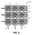
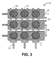
図1から図3および図5は、本開示の実施態様例による相互容量式タッチパネル100の例を示したものである。容量性タッチパネル100を使用して、必ずしもそれらに限定されないが、オールインワンコンピュータ、モバイル計算デバイス(たとえばハンドヘルド携帯型コンピュータ、携帯情報端末(PDA)、ラップトップコンピュータ、ネットブックコンピュータ、タブレットコンピュータ、等々)、モバイル電話デバイス(たとえばセルラー電話およびスマートフォン)、携帯型ゲームデバイス、携帯型メディアプレーヤ、マルチメディアデバイス、衛星ナビゲーションデバイス(たとえば全地球測位システム(GPS)ナビゲーションデバイス)、電子ブックリーダデバイス(eReader)、スマートテレビジョン(TV)デバイス、表面計算デバイス(たとえば卓上コンピュータ)、パーソナルコンピュータ(PC)デバイスを含む電子デバイス、ならびに接触をベースとする人間インターフェースを使用している他のデバイスとインターフェースすることができる。
Exemplary Embodiment FIGS. 1 to 3 and 5 show an example of a mutual
容量性タッチパネル100は、互いに隣り合わせに配置された(たとえば平行トラック、ほぼ平行のトラック、等々に沿って)クロスバーITO駆動トレース/トラックなどの駆動電極102を含んだITOタッチパネルを備えることができる。実施態様では、駆動電極102は、高度に導電性の、光学的に透明な水平方向および/または垂直方向のスピン/バーを使用して形成することができる。バーは、行トレースおよび/または列トレースの抵抗を小さくすることができ、したがってパネル全体に渡る位相シフトが小さくなり、また、接触コントローラ回路機構の複雑性が緩和される。駆動電極102は、細長く延びている(たとえば縦軸に沿って延在している)。たとえば各駆動電極102は、容量性タッチパネル100の基板などの支持表面の軸に沿って延在することができる。駆動電極102は、ピッチ106(たとえば駆動電極102の隣接する軸間の実質的に反復性の間隔)を有している。実施態様では、駆動電極102は、駆動電極102の隣接する縁間の最短距離からなる特性間隔108を同じく有している。
The
また、容量性タッチパネル100は、駆動電極102を横切って互いに隣り合わせに配置された(たとえば平行トラック、ほぼ平行のトラック、等々に沿って)クロスバーITOセンサトレース/トラックなどのセンサ電極110を同じく含む。実施態様では、センサ電極110は、高度に導電性の、光学的に透明な水平方向および/または垂直方向のスピン/バー(たとえばすでに説明したスピン/バー)を使用して形成することができる。センサ電極110は、細長く延びている(たとえば縦軸に沿って延在している)。たとえば各センサ電極110は、容量性タッチパネル100の基板などの支持表面の軸に沿って延在することができる。センサ電極110は、ピッチ112(たとえばセンサ電極110の隣接する軸間の実質的に反復性の間隔)を有している。センサ電極110は、「二重バー」構成を有するものとして示されているが、本開示によれば、他のセンサ電極110構成を利用することも可能であることを理解されたい(たとえば「単一バー」構成、突起を有する電極、等々)。
The
実施態様では、ピッチ112は、指の接触径に基づいている。たとえば隣接するセンサ電極110間のピッチ112は、中心間で約5ミリメートル(5mm)にすることができる。しかしながら5ミリメートル(5mm)のピッチ112は、単なる例として提供されたものであり、本開示を制限することを意味しているわけではない。したがって他の実施態様は、5ミリメートル(5mm)よりも広いピッチ112、または5ミリメートル(5mm)よりも狭いピッチ112を有することも可能である。
In an embodiment, the pitch 112 is based on the contact diameter of the finger. For example, the pitch 112 between
駆動電極102およびセンサ電極110は座標系を画定しており、各座標位置(ピクセル113)は、駆動電極102のうちの1つと、センサ電極110のうちの1つとの間の各交点に形成されるコンデンサを備えている。したがって駆動電極102は、各コンデンサに局部静電界を生成するための電圧源(または電流源)に接続されるように構成されており、各コンデンサ部分における指および/またはスタイラスによって生成される局部静電界の変化によって、対応する座標位置における接触と結合した容量が小さくなる。この方法によれば、異なる座標位置における複数の接触を同時に(または少なくとも実質的に同時に)知覚することができる。実施態様では、駆動電極102は、電圧源(または電流源)によって並列に駆動することができ、たとえば一組の異なる信号が駆動電極102に提供される。他の実施態様では、駆動電極102は、電圧源(または電流源)によって直列に駆動することができ、たとえば各駆動電極102または駆動電極102のサブセットが一度に1つずつ駆動される。
The
図1から図3に示されているように、タッチパネル100は誘電体構造104を含み、誘電体構造104は、センサ電極110の上に配置されている。1つまたは複数の実施態様では、誘電体構造104は、所望のパターンを提供し、および/または電気変位場を導くために、約10ナノメートルから約100ナノメートルまでの範囲に及ぶ厚さを有することができる。図4に示されているように、誘電体構造104は、誘電材料の複数の層を備えることができる。たとえば誘電体構造104は、第1の誘電材料104(1)、第2の誘電材料104(2)、第3の誘電材料104(3)、等々を含むことができる。
As shown in FIGS. 1 to 3, the
いくつかの実施態様では、様々な誘電材料は、同じ誘電材料、異なる誘電材料(互いに対して)またはそれらの組合せからなっていてもよい。誘電材料は、タッチパネル100の要求事項に基づいて選択することができることが企図されている。いくつかの実施態様では、誘電材料は、五酸化ニオブ(Nb2O5)、二酸化チタン(TiO2)、等々からなっていてもよい。たとえば誘電材料は、所望のパターンを提供し、および/または電気変位場を導くために、約20から約100までの範囲に及ぶ比誘電率を有する誘電材料を選択することができる。しかしながらいくつかの実例では、チタン酸バリウム(BaTiO3)などのより大きい誘電率を有する強誘電体を利用することができる。誘電材料は、所望のパターンを提供し、および/または電気変位場を導くために、容量結合を修正するように選択される。したがって容量結合および/または静電界の所望のパターンは、誘電体構造104のために選択される誘電材料のタイプを指示することができる。
In some implementations, the various dielectric materials may consist of the same dielectric material, different dielectric materials (relative to each other), or combinations thereof. It is contemplated that the dielectric material can be selected based on the requirements of the
図1および図2に示されているように、誘電体構造104は、様々な方法で構成することができる。たとえば図1に示されているように、タッチパネル100は、長方形構成で構成された誘電体構造104を含み、また、図2に示されているように、タッチパネルは、ひし形構成で構成された誘電体構造104を含む。図2に示されているひし形構成を参照すると、ひし形パターンの誘電体構造104は、ピクセル中心113から緩やかな先細りを提供している。緩やかな先細りは、静電界の正確で滑らかな局部化を提供することができる。別の実施態様では、図3に示されているように、タッチパネル100は、円形構成で構成された誘電体構造104を含む。設計の要求事項に応じて他の形状を利用することができることが企図されている。
As shown in FIGS. 1 and 2, the
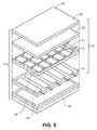
図5に示されているように、センサ電極110は、駆動電極102から電気絶縁されている(たとえば誘電体層、等々を使用して)。たとえばセンサ電極110は、1つの基板(たとえばガラス基板の上に配置されたセンサ層114を備えた)の上に提供することができ、また、駆動電極102は、別の基板(たとえば別の基板の上に配置された駆動層116を備えた)の上に提供することができる。この2層構成では、センサ層114は、駆動層116の上方に配置することができる(たとえば接触表面に対して)。たとえばセンサ層114は、駆動層116よりも接触表面の近くに配置することができる。しかしながらこの構成は、単なる例として提供されたものであり、本開示を制限することを意味しているわけではない。したがって、駆動層116がセンサ層114よりも接触表面の近くに配置され、および/またはセンサ層114および駆動層116が同じ層を備える他の構成を提供することも可能である。
As shown in FIG. 5, the
1つまたは複数の容量性タッチパネル100は、タッチスクリーンアセンブリ118とともに含まれ得る。タッチスクリーンアセンブリ118は、LCDスクリーン120などのディスプレイスクリーンを含むことができ、センサ層114および駆動層116は、LCDスクリーン120と、たとえば保護カバー124(たとえばガラス)が取り付けられた結合層122との間に配置される。保護カバー124は、保護コーティング、無反射コーティング、等々を含むことができる。保護カバー124は接触表面126を備えることができ、オペレータは、この接触表面126の上で、1本または複数本の指、スタイラス、等々を使用して、コマンドをタッチスクリーンアセンブリ118に入力することができる。コマンドを使用して、たとえばLCDスクリーン120によって表示される図形を操作することができる。さらに、コマンドは、容量性タッチパネル100に接続された、マルチメディアデバイスなどの電子デバイス、または別の電子デバイス(たとえばすでに説明したような電子デバイス)への入力として使用することも可能である。
One or more
プロセス例
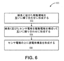
次に図6を参照すると、誘電体構造が中に形成された容量性タッチパネルを供給するための技法の例が記述されている。
Example Process Referring now to FIG. 6, an example technique for providing a capacitive touch panel having a dielectric structure formed therein is described.
図6は、一実施態様例における、図1から図5に示され、かつ、上で説明した容量性タッチパネル100などの容量性タッチパネルを供給するためのプロセス600を示したものである。示されているプロセス600では、互いに隣り合わせに配置された、細長く延びた駆動電極が形成される(ブロック602)。たとえば図1から図5を参照すると、クロスバーITO駆動トレース/トラックなどの駆動電極102は、互いに隣り合わせに配置される。駆動電極102は、高度に導電性の、光学的に透明な水平方向および/または垂直方向のバーを使用して、容量性タッチパネル100の基板の上に形成することができる。
FIG. 6 shows a
次に、駆動電極を横切って互いに隣り合わせに配置された、細長く延びたセンサ電極が形成される(ブロック604)。たとえば引き続いて図1から図5を参照すると、クロスバーITOセンサトレース/トラックなどのセンサ電極110は、駆動電極102を横切って互いに隣り合わせに配置される。センサ電極110は、高度に導電性の、光学的に透明な水平方向および/または垂直方向のバーを使用して、容量性タッチパネル100の基板の上に形成することができる。次に、図6に示されているように、誘電体構造がセンサ電極の上に形成される(ブロック606)。たとえば図1から図3に示されているように、複数の誘電体構造104がセンサ電極102の上に形成される。一実施態様では、誘電体構造104は、誘電体構造104がタッチパネル100のピクセル中心113の上に配置されるように形成される。1つまたは複数の実施態様では、誘電体構造104は、適切な堆積プロセスを利用して形成される。たとえば誘電体構造104は、適切な薄膜プロセス、厚膜プロセス、等々を利用して形成することができる。一実施態様例では、誘電体構造104は、センサ電極110の上に直接形成される。
Next, elongated sensor electrodes are formed that are positioned next to each other across the drive electrodes (block 604). For example, with continued reference to FIGS. 1-5,
結論
以上、主題について、構造的特徴および/またはプロセス操作に特化された言語で説明したが、添付の特許請求の範囲で定義されている主題は、必ずしも上で説明した特定の特徴または動作に限定されないことを理解されたい。そうではなく、上で説明した特定の特徴および動作は、特許請求の範囲を実現する例示的形態として開示されている。
CONCLUSION While the subject matter has been described in language specific to structural features and / or process operations, the subject matter defined in the appended claims does not necessarily refer to a particular feature or action described above. It should be understood that it is not limited. Rather, the specific features and acts described above are disclosed as example forms of implementing the claims.
100 相互容量式タッチパネル、容量性タッチパネル
102 駆動電極
106、112 ピッチ
104 誘電体構造
104(1) 第1の誘電材料
104(2) 第2の誘電材料
104(3) 第3の誘電材料
108 特性間隔
110 センサ電極
113 ピクセル、ピクセル中心
114 センサ層
116 駆動層
118 タッチスクリーンアセンブリ
120 LCDスクリーン
122 結合層
124 保護カバー
126 接触表面
DESCRIPTION OF
Claims (20)
前記複数の細長く延びた駆動電極を横切って互いに隣り合わせに配置された、複数の細長く延びたセンサ電極と、
前記複数のセンサ電極のうちの少なくとも1つのセンサ電極の上に配置された少なくとも1つの誘電体構造と
を備えている相互容量式タッチパネル。 A plurality of elongated drive electrodes arranged next to each other;
A plurality of elongated sensor electrodes disposed adjacent to each other across the plurality of elongated drive electrodes;
A mutual capacitive touch panel comprising: at least one dielectric structure disposed on at least one of the plurality of sensor electrodes.
互いに隣り合わせに配置された、複数の細長く延びた駆動電極を形成するステップと、
前記複数の細長く延びた駆動電極を横切って互いに隣り合わせに配置された、複数の細長く延びたセンサ電極を形成するステップと、
前記複数のセンサ電極のうちの少なくとも1つのセンサ電極の上に少なくとも1つの誘電体構造を形成するステップと
を含む方法。 A method of forming a mutual capacitive touch panel,
Forming a plurality of elongated drive electrodes disposed next to each other;
Forming a plurality of elongated sensor electrodes disposed adjacent to each other across the plurality of elongated drive electrodes;
Forming at least one dielectric structure on at least one sensor electrode of the plurality of sensor electrodes.
前記複数の細長く延びた駆動電極を横切って互いに隣り合わせに配置された、複数の細長く延びたセンサ電極であって、前記複数の細長く延びた駆動電極および前記複数のセンサ電極が、細長く延びた各駆動電極と細長く延びた各センサ電極のそれぞれの交点にピクセルを画定する、複数の細長く延びたセンサ電極と、
それぞれの交点の上に配置された複数の誘電体構造と
を備えている相互容量式タッチパネル。 A plurality of elongated drive electrodes arranged next to each other;
A plurality of elongated sensor electrodes disposed adjacent to each other across the plurality of elongated drive electrodes, wherein each of the plurality of elongated drive electrodes and the plurality of sensor electrodes is elongated. A plurality of elongated sensor electrodes defining a pixel at each intersection of the electrodes and each elongated sensor electrode;
A mutual capacitive touch panel comprising a plurality of dielectric structures arranged on each intersection.
Applications Claiming Priority (3)
| Application Number | Priority Date | Filing Date | Title |
|---|---|---|---|
| US201462014761P | 2014-06-20 | 2014-06-20 | |
| US62/014,761 | 2014-06-20 | ||
| PCT/US2015/036375 WO2015195878A1 (en) | 2014-06-20 | 2015-06-18 | Capacitive touch panel having dielectric structures formed therein |
Publications (2)
| Publication Number | Publication Date |
|---|---|
| JP2017518586A true JP2017518586A (en) | 2017-07-06 |
| JP2017518586A5 JP2017518586A5 (en) | 2018-07-12 |
Family
ID=54869612
Family Applications (1)
| Application Number | Title | Priority Date | Filing Date |
|---|---|---|---|
| JP2016573091A Pending JP2017518586A (en) | 2014-06-20 | 2015-06-18 | Capacitive touch panel with dielectric structure formed inside |
Country Status (5)
| Country | Link |
|---|---|
| US (1) | US20150370372A1 (en) |
| EP (1) | EP3158423A4 (en) |
| JP (1) | JP2017518586A (en) |
| CN (1) | CN106415464A (en) |
| WO (1) | WO2015195878A1 (en) |
Families Citing this family (3)
| Publication number | Priority date | Publication date | Assignee | Title |
|---|---|---|---|---|
| KR102214929B1 (en) * | 2013-04-15 | 2021-02-10 | 삼성전자주식회사 | Apparatus and method for providing tactile |
| KR20160028067A (en) * | 2014-09-02 | 2016-03-11 | 엘지디스플레이 주식회사 | Mobile terminal device and driving method thereof |
| JP2018190022A (en) * | 2017-04-28 | 2018-11-29 | 株式会社Vtsタッチセンサー | Touch panel and display apparatus using the same |
Citations (7)
| Publication number | Priority date | Publication date | Assignee | Title |
|---|---|---|---|---|
| US20090002337A1 (en) * | 2007-06-28 | 2009-01-01 | Sense Pad Tech Co., Ltd | Capacitive-type touch panel |
| WO2011081112A1 (en) * | 2009-12-28 | 2011-07-07 | 京セラ株式会社 | Input device and display device provided with same |
| US20110221687A1 (en) * | 2010-03-10 | 2011-09-15 | Tpk Touch Solutions Inc. | Electrode pattern structure of a capacitive touch panel and method of manufacturing the same |
| WO2011137606A1 (en) * | 2010-05-04 | 2011-11-10 | Tpk Touch Solutions Inc. | Capacitive touch sensing structure, process of producing the same and touch sensing device using the same |
| JP2012081663A (en) * | 2010-10-12 | 2012-04-26 | Sumitomo Metal Mining Co Ltd | Transparent electrically conductive base material, and touch panel |
| US20130009653A1 (en) * | 2011-07-08 | 2013-01-10 | Wacom Co., Ltd. | Position detecting sensor, position detecting device, and position detecting method |
| WO2013117815A1 (en) * | 2012-02-06 | 2013-08-15 | Canatu Oy | A touch sensing device and a detection method |
Family Cites Families (13)
| Publication number | Priority date | Publication date | Assignee | Title |
|---|---|---|---|---|
| US20080309633A1 (en) * | 2007-06-13 | 2008-12-18 | Apple Inc. | Touch-sensitive display |
| JP5753084B2 (en) * | 2008-08-01 | 2015-07-22 | スリーエム イノベイティブ プロパティズ カンパニー | Manufacturing method of composite electrode |
| US7958789B2 (en) * | 2008-08-08 | 2011-06-14 | Tokai Rubber Industries, Ltd. | Capacitive sensor |
| US8976117B2 (en) * | 2010-09-01 | 2015-03-10 | Google Technology Holdings LLC | Keypad with integrated touch sensitive apparatus |
| KR101230196B1 (en) * | 2010-10-29 | 2013-02-06 | 삼성디스플레이 주식회사 | Liquid Crystal Display having a Touch Screen Panel |
| TWI403939B (en) * | 2010-12-31 | 2013-08-01 | Au Optronics Corp | Touch panel and touch display panel |
| TW201234243A (en) * | 2011-02-01 | 2012-08-16 | Ind Tech Res Inst | Projective capacitive touch sensor structure and fabricating method thereof |
| US20130154996A1 (en) * | 2011-12-16 | 2013-06-20 | Matthew Trend | Touch Sensor Including Mutual Capacitance Electrodes and Self-Capacitance Electrodes |
| US20130194198A1 (en) * | 2012-02-01 | 2013-08-01 | David Brent GUARD | Thin Dielectric Layer For Touch Sensor Stack |
| US9817523B2 (en) * | 2012-02-09 | 2017-11-14 | Qualcomm Incorporated | Capacitive touch panel for mitigating and/or exaggerating floating condition effects |
| CN103970374A (en) * | 2013-01-28 | 2014-08-06 | 宸鸿科技(厦门)有限公司 | Touch control unit and touch control panel |
| US20140354577A1 (en) * | 2013-05-28 | 2014-12-04 | Ingar Hanssen | Multi-State Capacitive Button |
| CN103543895A (en) * | 2013-09-30 | 2014-01-29 | 领威联芯(北京)科技有限公司 | Electrode device of touch screen and mutual capacitance touch screen using electrode device |
-
2015
- 2015-06-18 EP EP15810344.0A patent/EP3158423A4/en not_active Withdrawn
- 2015-06-18 US US14/743,065 patent/US20150370372A1/en not_active Abandoned
- 2015-06-18 CN CN201580030232.4A patent/CN106415464A/en active Pending
- 2015-06-18 WO PCT/US2015/036375 patent/WO2015195878A1/en active Application Filing
- 2015-06-18 JP JP2016573091A patent/JP2017518586A/en active Pending
Patent Citations (11)
| Publication number | Priority date | Publication date | Assignee | Title |
|---|---|---|---|---|
| US20090002337A1 (en) * | 2007-06-28 | 2009-01-01 | Sense Pad Tech Co., Ltd | Capacitive-type touch panel |
| JP2009009574A (en) * | 2007-06-28 | 2009-01-15 | Sense Pad Tech Co Ltd | Capacitive-type touch panel |
| WO2011081112A1 (en) * | 2009-12-28 | 2011-07-07 | 京セラ株式会社 | Input device and display device provided with same |
| US20120182250A1 (en) * | 2009-12-28 | 2012-07-19 | Kyocera Corporation | Input device and display device provided with same |
| US20110221687A1 (en) * | 2010-03-10 | 2011-09-15 | Tpk Touch Solutions Inc. | Electrode pattern structure of a capacitive touch panel and method of manufacturing the same |
| WO2011137606A1 (en) * | 2010-05-04 | 2011-11-10 | Tpk Touch Solutions Inc. | Capacitive touch sensing structure, process of producing the same and touch sensing device using the same |
| JP2013525925A (en) * | 2010-05-04 | 2013-06-20 | ティーピーケイ タッチ ソリューションズ インコーポレーテッド | Capacitive touch sensor system, production process thereof, and touch sensor device using the same |
| JP2012081663A (en) * | 2010-10-12 | 2012-04-26 | Sumitomo Metal Mining Co Ltd | Transparent electrically conductive base material, and touch panel |
| US20130009653A1 (en) * | 2011-07-08 | 2013-01-10 | Wacom Co., Ltd. | Position detecting sensor, position detecting device, and position detecting method |
| JP2013020370A (en) * | 2011-07-08 | 2013-01-31 | Wacom Co Ltd | Position detection sensor, position detector, and position detection method |
| WO2013117815A1 (en) * | 2012-02-06 | 2013-08-15 | Canatu Oy | A touch sensing device and a detection method |
Also Published As
| Publication number | Publication date |
|---|---|
| CN106415464A (en) | 2017-02-15 |
| EP3158423A1 (en) | 2017-04-26 |
| EP3158423A4 (en) | 2018-01-17 |
| US20150370372A1 (en) | 2015-12-24 |
| WO2015195878A1 (en) | 2015-12-23 |
Similar Documents
| Publication | Publication Date | Title |
|---|---|---|
| US9116582B2 (en) | Capacitive touch panel having protrusions formed between drive and/or sensor electrodes | |
| US10444891B2 (en) | Touch panel and display device including the same | |
| US9817523B2 (en) | Capacitive touch panel for mitigating and/or exaggerating floating condition effects | |
| US10540043B2 (en) | Hybrid in-cell sensor topology | |
| TWI625667B (en) | Capacitive touch sensor panel, digital audio player, and method for shielding a capacitive touch sensor panel | |
| US9098153B2 (en) | Touch panel excitation using a drive signal having time-varying characteristics | |
| US9927832B2 (en) | Input device having a reduced border region | |
| US10133421B2 (en) | Display stackups for matrix sensor | |
| CN103513842A (en) | Touch screen panel | |
| JP2008217784A (en) | Touch panel | |
| US10048796B2 (en) | Touch module, touch screen panel, touch positioning method thereof and display device | |
| US20150220175A1 (en) | Capacitive touch panel and display device | |
| US20170010724A1 (en) | Liquid crystal display device with touch-sensing function and conductive layer structure thereof | |
| US11635858B2 (en) | Excitation schemes for an input device | |
| KR20160068466A (en) | Display pannel, touch input device, device for detecting touch position and touch pressure from the display pannel, and method for detecting touch position and touch pressure | |
| US10656744B2 (en) | Thin film transistor array substrate and touch display panel using same | |
| JP2017518586A (en) | Capacitive touch panel with dielectric structure formed inside | |
| US20140104221A1 (en) | Capacitive touch panel sensor for mitigating effects of a floating condition | |
| CN114077363A (en) | Balanced mutual capacitance system and method | |
| US9423896B2 (en) | Method for representing a tactile image and touch screen apparatus for performing the method | |
| US9285935B2 (en) | Touch screen device | |
| KR20160080069A (en) | Touch panel and display device including the same | |
| US20210089170A1 (en) | Spherical or highly curved touch-sensitive surfaces | |
| US10809843B2 (en) | Touch sensor signal integration | |
| KR101380817B1 (en) | Self capacitive touch panel apparatus and touch location recognition method in the same |
Legal Events
| Date | Code | Title | Description |
|---|---|---|---|
| A521 | Request for written amendment filed |
Free format text: JAPANESE INTERMEDIATE CODE: A523 Effective date: 20161221 |
|
| A521 | Request for written amendment filed |
Free format text: JAPANESE INTERMEDIATE CODE: A523 Effective date: 20180528 |
|
| A621 | Written request for application examination |
Free format text: JAPANESE INTERMEDIATE CODE: A621 Effective date: 20180528 |
|
| A977 | Report on retrieval |
Free format text: JAPANESE INTERMEDIATE CODE: A971007 Effective date: 20190222 |
|
| A131 | Notification of reasons for refusal |
Free format text: JAPANESE INTERMEDIATE CODE: A131 Effective date: 20190311 |
|
| A02 | Decision of refusal |
Free format text: JAPANESE INTERMEDIATE CODE: A02 Effective date: 20191028 |