JP2011530167A - Transistor with embedded Si / Ge material with enhanced boron confinement - Google Patents
Transistor with embedded Si / Ge material with enhanced boron confinement Download PDFInfo
- Publication number
- JP2011530167A JP2011530167A JP2011521127A JP2011521127A JP2011530167A JP 2011530167 A JP2011530167 A JP 2011530167A JP 2011521127 A JP2011521127 A JP 2011521127A JP 2011521127 A JP2011521127 A JP 2011521127A JP 2011530167 A JP2011530167 A JP 2011530167A
- Authority
- JP
- Japan
- Prior art keywords
- diffusion
- drain
- region
- transistor
- species
- Prior art date
- Legal status (The legal status is an assumption and is not a legal conclusion. Google has not performed a legal analysis and makes no representation as to the accuracy of the status listed.)
- Pending
Links
- 239000000463 material Substances 0.000 title claims description 54
- ZOXJGFHDIHLPTG-UHFFFAOYSA-N Boron Chemical compound [B] ZOXJGFHDIHLPTG-UHFFFAOYSA-N 0.000 title claims description 25
- 229910052796 boron Inorganic materials 0.000 title claims description 25
- 238000009792 diffusion process Methods 0.000 claims abstract description 96
- 230000002401 inhibitory effect Effects 0.000 claims abstract description 63
- IJGRMHOSHXDMSA-UHFFFAOYSA-N Atomic nitrogen Chemical compound N#N IJGRMHOSHXDMSA-UHFFFAOYSA-N 0.000 claims abstract description 24
- OKTJSMMVPCPJKN-UHFFFAOYSA-N Carbon Chemical compound [C] OKTJSMMVPCPJKN-UHFFFAOYSA-N 0.000 claims abstract description 12
- 229910052799 carbon Inorganic materials 0.000 claims abstract description 12
- 229910052757 nitrogen Inorganic materials 0.000 claims abstract description 12
- 238000000034 method Methods 0.000 claims description 138
- 239000004065 semiconductor Substances 0.000 claims description 128
- 230000008569 process Effects 0.000 claims description 98
- 229910045601 alloy Inorganic materials 0.000 claims description 45
- 239000000956 alloy Substances 0.000 claims description 45
- 239000002019 doping agent Substances 0.000 claims description 45
- 238000005530 etching Methods 0.000 claims description 41
- 239000013078 crystal Substances 0.000 claims description 40
- 238000002513 implantation Methods 0.000 claims description 27
- 230000001939 inductive effect Effects 0.000 claims description 26
- 238000000137 annealing Methods 0.000 claims description 12
- 239000000758 substrate Substances 0.000 claims description 9
- PXGOKWXKJXAPGV-UHFFFAOYSA-N Fluorine Chemical compound FF PXGOKWXKJXAPGV-UHFFFAOYSA-N 0.000 claims description 5
- 229910052731 fluorine Inorganic materials 0.000 claims description 5
- 239000011737 fluorine Substances 0.000 claims description 5
- 238000002347 injection Methods 0.000 claims description 5
- 239000007924 injection Substances 0.000 claims description 5
- 230000005669 field effect Effects 0.000 claims description 3
- 239000010703 silicon Substances 0.000 abstract description 33
- 230000002829 reductive effect Effects 0.000 abstract description 21
- 229910000927 Ge alloy Inorganic materials 0.000 abstract description 9
- 229910000676 Si alloy Inorganic materials 0.000 abstract description 9
- 230000000087 stabilizing effect Effects 0.000 abstract 1
- 238000004519 manufacturing process Methods 0.000 description 33
- XUIMIQQOPSSXEZ-UHFFFAOYSA-N Silicon Chemical compound [Si] XUIMIQQOPSSXEZ-UHFFFAOYSA-N 0.000 description 32
- 229910052710 silicon Inorganic materials 0.000 description 24
- 125000006850 spacer group Chemical group 0.000 description 23
- 230000007547 defect Effects 0.000 description 16
- 230000000694 effects Effects 0.000 description 16
- 230000001965 increasing effect Effects 0.000 description 15
- 229910052732 germanium Inorganic materials 0.000 description 12
- GNPVGFCGXDBREM-UHFFFAOYSA-N germanium atom Chemical compound [Ge] GNPVGFCGXDBREM-UHFFFAOYSA-N 0.000 description 12
- 230000006399 behavior Effects 0.000 description 10
- 238000005516 engineering process Methods 0.000 description 8
- 230000008901 benefit Effects 0.000 description 7
- 230000009467 reduction Effects 0.000 description 7
- 229910052581 Si3N4 Inorganic materials 0.000 description 6
- 230000015572 biosynthetic process Effects 0.000 description 6
- HQVNEWCFYHHQES-UHFFFAOYSA-N silicon nitride Chemical compound N12[Si]34N5[Si]62N3[Si]51N64 HQVNEWCFYHHQES-UHFFFAOYSA-N 0.000 description 6
- 238000013459 approach Methods 0.000 description 5
- 125000004429 atom Chemical group 0.000 description 5
- 230000008021 deposition Effects 0.000 description 5
- 238000000151 deposition Methods 0.000 description 5
- 230000003071 parasitic effect Effects 0.000 description 5
- 238000013461 design Methods 0.000 description 4
- 239000003989 dielectric material Substances 0.000 description 4
- 238000005468 ion implantation Methods 0.000 description 4
- 238000002955 isolation Methods 0.000 description 4
- 230000007246 mechanism Effects 0.000 description 4
- 238000012545 processing Methods 0.000 description 4
- 239000002800 charge carrier Substances 0.000 description 3
- 238000011161 development Methods 0.000 description 3
- 230000018109 developmental process Effects 0.000 description 3
- 239000007772 electrode material Substances 0.000 description 3
- 239000007943 implant Substances 0.000 description 3
- 230000006872 improvement Effects 0.000 description 3
- 238000000059 patterning Methods 0.000 description 3
- VYPSYNLAJGMNEJ-UHFFFAOYSA-N Silicium dioxide Chemical compound O=[Si]=O VYPSYNLAJGMNEJ-UHFFFAOYSA-N 0.000 description 2
- 230000006978 adaptation Effects 0.000 description 2
- 230000002708 enhancing effect Effects 0.000 description 2
- 238000011049 filling Methods 0.000 description 2
- 230000006870 function Effects 0.000 description 2
- 125000005843 halogen group Chemical group 0.000 description 2
- 238000010348 incorporation Methods 0.000 description 2
- 230000006698 induction Effects 0.000 description 2
- 230000005764 inhibitory process Effects 0.000 description 2
- 238000012986 modification Methods 0.000 description 2
- 230000004048 modification Effects 0.000 description 2
- 239000002210 silicon-based material Substances 0.000 description 2
- 229910015900 BF3 Inorganic materials 0.000 description 1
- 229910000577 Silicon-germanium Inorganic materials 0.000 description 1
- LEVVHYCKPQWKOP-UHFFFAOYSA-N [Si].[Ge] Chemical compound [Si].[Ge] LEVVHYCKPQWKOP-UHFFFAOYSA-N 0.000 description 1
- 238000000429 assembly Methods 0.000 description 1
- 230000000712 assembly Effects 0.000 description 1
- -1 boron fluoride ions Chemical class 0.000 description 1
- 239000012876 carrier material Substances 0.000 description 1
- 230000008859 change Effects 0.000 description 1
- 230000000295 complement effect Effects 0.000 description 1
- 238000010276 construction Methods 0.000 description 1
- 230000008878 coupling Effects 0.000 description 1
- 238000010168 coupling process Methods 0.000 description 1
- 238000005859 coupling reaction Methods 0.000 description 1
- 239000002178 crystalline material Substances 0.000 description 1
- 229910021419 crystalline silicon Inorganic materials 0.000 description 1
- 238000010586 diagram Methods 0.000 description 1
- OKZIUSOJQLYFSE-UHFFFAOYSA-N difluoroboron Chemical compound F[B]F OKZIUSOJQLYFSE-UHFFFAOYSA-N 0.000 description 1
- 238000009499 grossing Methods 0.000 description 1
- 238000010438 heat treatment Methods 0.000 description 1
- 238000001802 infusion Methods 0.000 description 1
- 239000012212 insulator Substances 0.000 description 1
- 150000002500 ions Chemical class 0.000 description 1
- 230000000670 limiting effect Effects 0.000 description 1
- 238000001459 lithography Methods 0.000 description 1
- 230000000873 masking effect Effects 0.000 description 1
- 229920000620 organic polymer Polymers 0.000 description 1
- RVTZCBVAJQQJTK-UHFFFAOYSA-N oxygen(2-);zirconium(4+) Chemical class [O-2].[O-2].[Zr+4] RVTZCBVAJQQJTK-UHFFFAOYSA-N 0.000 description 1
- 238000000206 photolithography Methods 0.000 description 1
- 229910021420 polycrystalline silicon Inorganic materials 0.000 description 1
- 239000002243 precursor Substances 0.000 description 1
- 230000008439 repair process Effects 0.000 description 1
- 239000000377 silicon dioxide Substances 0.000 description 1
- 235000012239 silicon dioxide Nutrition 0.000 description 1
- 238000004088 simulation Methods 0.000 description 1
- 239000000243 solution Substances 0.000 description 1
- 230000003068 static effect Effects 0.000 description 1
- 238000007669 thermal treatment Methods 0.000 description 1
- 229910001928 zirconium oxide Inorganic materials 0.000 description 1
Images


Classifications
-
- H—ELECTRICITY
- H01—ELECTRIC ELEMENTS
- H01L—SEMICONDUCTOR DEVICES NOT COVERED BY CLASS H10
- H01L21/00—Processes or apparatus adapted for the manufacture or treatment of semiconductor or solid state devices or of parts thereof
- H01L21/02—Manufacture or treatment of semiconductor devices or of parts thereof
- H01L21/04—Manufacture or treatment of semiconductor devices or of parts thereof the devices having at least one potential-jump barrier or surface barrier, e.g. PN junction, depletion layer or carrier concentration layer
- H01L21/18—Manufacture or treatment of semiconductor devices or of parts thereof the devices having at least one potential-jump barrier or surface barrier, e.g. PN junction, depletion layer or carrier concentration layer the devices having semiconductor bodies comprising elements of Group IV of the Periodic System or AIIIBV compounds with or without impurities, e.g. doping materials
- H01L21/26—Bombardment with radiation
- H01L21/263—Bombardment with radiation with high-energy radiation
- H01L21/265—Bombardment with radiation with high-energy radiation producing ion implantation
- H01L21/26506—Bombardment with radiation with high-energy radiation producing ion implantation in group IV semiconductors
- H01L21/26513—Bombardment with radiation with high-energy radiation producing ion implantation in group IV semiconductors of electrically active species
-
- H—ELECTRICITY
- H01—ELECTRIC ELEMENTS
- H01L—SEMICONDUCTOR DEVICES NOT COVERED BY CLASS H10
- H01L29/00—Semiconductor devices adapted for rectifying, amplifying, oscillating or switching, or capacitors or resistors with at least one potential-jump barrier or surface barrier, e.g. PN junction depletion layer or carrier concentration layer; Details of semiconductor bodies or of electrodes thereof ; Multistep manufacturing processes therefor
- H01L29/02—Semiconductor bodies ; Multistep manufacturing processes therefor
- H01L29/12—Semiconductor bodies ; Multistep manufacturing processes therefor characterised by the materials of which they are formed
- H01L29/16—Semiconductor bodies ; Multistep manufacturing processes therefor characterised by the materials of which they are formed including, apart from doping materials or other impurities, only elements of Group IV of the Periodic System
- H01L29/161—Semiconductor bodies ; Multistep manufacturing processes therefor characterised by the materials of which they are formed including, apart from doping materials or other impurities, only elements of Group IV of the Periodic System including two or more of the elements provided for in group H01L29/16, e.g. alloys
- H01L29/165—Semiconductor bodies ; Multistep manufacturing processes therefor characterised by the materials of which they are formed including, apart from doping materials or other impurities, only elements of Group IV of the Periodic System including two or more of the elements provided for in group H01L29/16, e.g. alloys in different semiconductor regions, e.g. heterojunctions
-
- H—ELECTRICITY
- H01—ELECTRIC ELEMENTS
- H01L—SEMICONDUCTOR DEVICES NOT COVERED BY CLASS H10
- H01L29/00—Semiconductor devices adapted for rectifying, amplifying, oscillating or switching, or capacitors or resistors with at least one potential-jump barrier or surface barrier, e.g. PN junction depletion layer or carrier concentration layer; Details of semiconductor bodies or of electrodes thereof ; Multistep manufacturing processes therefor
- H01L29/66—Types of semiconductor device ; Multistep manufacturing processes therefor
- H01L29/66007—Multistep manufacturing processes
- H01L29/66075—Multistep manufacturing processes of devices having semiconductor bodies comprising group 14 or group 13/15 materials
- H01L29/66227—Multistep manufacturing processes of devices having semiconductor bodies comprising group 14 or group 13/15 materials the devices being controllable only by the electric current supplied or the electric potential applied, to an electrode which does not carry the current to be rectified, amplified or switched, e.g. three-terminal devices
- H01L29/66409—Unipolar field-effect transistors
- H01L29/66477—Unipolar field-effect transistors with an insulated gate, i.e. MISFET
- H01L29/66568—Lateral single gate silicon transistors
- H01L29/66575—Lateral single gate silicon transistors where the source and drain or source and drain extensions are self-aligned to the sides of the gate
- H01L29/6659—Lateral single gate silicon transistors where the source and drain or source and drain extensions are self-aligned to the sides of the gate with both lightly doped source and drain extensions and source and drain self-aligned to the sides of the gate, e.g. lightly doped drain [LDD] MOSFET, double diffused drain [DDD] MOSFET
-
- H—ELECTRICITY
- H01—ELECTRIC ELEMENTS
- H01L—SEMICONDUCTOR DEVICES NOT COVERED BY CLASS H10
- H01L29/00—Semiconductor devices adapted for rectifying, amplifying, oscillating or switching, or capacitors or resistors with at least one potential-jump barrier or surface barrier, e.g. PN junction depletion layer or carrier concentration layer; Details of semiconductor bodies or of electrodes thereof ; Multistep manufacturing processes therefor
- H01L29/66—Types of semiconductor device ; Multistep manufacturing processes therefor
- H01L29/66007—Multistep manufacturing processes
- H01L29/66075—Multistep manufacturing processes of devices having semiconductor bodies comprising group 14 or group 13/15 materials
- H01L29/66227—Multistep manufacturing processes of devices having semiconductor bodies comprising group 14 or group 13/15 materials the devices being controllable only by the electric current supplied or the electric potential applied, to an electrode which does not carry the current to be rectified, amplified or switched, e.g. three-terminal devices
- H01L29/66409—Unipolar field-effect transistors
- H01L29/66477—Unipolar field-effect transistors with an insulated gate, i.e. MISFET
- H01L29/66568—Lateral single gate silicon transistors
- H01L29/66636—Lateral single gate silicon transistors with source or drain recessed by etching or first recessed by etching and then refilled
-
- H—ELECTRICITY
- H01—ELECTRIC ELEMENTS
- H01L—SEMICONDUCTOR DEVICES NOT COVERED BY CLASS H10
- H01L29/00—Semiconductor devices adapted for rectifying, amplifying, oscillating or switching, or capacitors or resistors with at least one potential-jump barrier or surface barrier, e.g. PN junction depletion layer or carrier concentration layer; Details of semiconductor bodies or of electrodes thereof ; Multistep manufacturing processes therefor
- H01L29/66—Types of semiconductor device ; Multistep manufacturing processes therefor
- H01L29/68—Types of semiconductor device ; Multistep manufacturing processes therefor controllable by only the electric current supplied, or only the electric potential applied, to an electrode which does not carry the current to be rectified, amplified or switched
- H01L29/76—Unipolar devices, e.g. field effect transistors
- H01L29/772—Field effect transistors
- H01L29/78—Field effect transistors with field effect produced by an insulated gate
- H01L29/7833—Field effect transistors with field effect produced by an insulated gate with lightly doped drain or source extension, e.g. LDD MOSFET's; DDD MOSFET's
- H01L29/7834—Field effect transistors with field effect produced by an insulated gate with lightly doped drain or source extension, e.g. LDD MOSFET's; DDD MOSFET's with a non-planar structure, e.g. the gate or the source or the drain being non-planar
-
- H—ELECTRICITY
- H01—ELECTRIC ELEMENTS
- H01L—SEMICONDUCTOR DEVICES NOT COVERED BY CLASS H10
- H01L29/00—Semiconductor devices adapted for rectifying, amplifying, oscillating or switching, or capacitors or resistors with at least one potential-jump barrier or surface barrier, e.g. PN junction depletion layer or carrier concentration layer; Details of semiconductor bodies or of electrodes thereof ; Multistep manufacturing processes therefor
- H01L29/66—Types of semiconductor device ; Multistep manufacturing processes therefor
- H01L29/68—Types of semiconductor device ; Multistep manufacturing processes therefor controllable by only the electric current supplied, or only the electric potential applied, to an electrode which does not carry the current to be rectified, amplified or switched
- H01L29/76—Unipolar devices, e.g. field effect transistors
- H01L29/772—Field effect transistors
- H01L29/78—Field effect transistors with field effect produced by an insulated gate
- H01L29/7842—Field effect transistors with field effect produced by an insulated gate means for exerting mechanical stress on the crystal lattice of the channel region, e.g. using a flexible substrate
- H01L29/7848—Field effect transistors with field effect produced by an insulated gate means for exerting mechanical stress on the crystal lattice of the channel region, e.g. using a flexible substrate the means being located in the source/drain region, e.g. SiGe source and drain
Abstract
【解決手段】
シリコン/ゲルマニウム合金(255)を備えたPチャネルトランジスタのPN接合の近傍に拡散阻害種(256A)を組み込むことによって、拡散関連のPM接合の不均一性を低減することができ、それによりデバイス安定性を高め且つ総合的なトランジスタ性能を高めることに寄与する。拡散阻害種(256A)は炭素、窒素等の形態で提供されてよい。
【選択図】図2e[Solution]
By incorporating diffusion-inhibiting species (256A) in the vicinity of the PN junction of a P-channel transistor with a silicon / germanium alloy (255), diffusion-related PM junction non-uniformity can be reduced, thereby stabilizing the device. This contributes to improving the performance and improving the overall transistor performance. The diffusion inhibiting species (256A) may be provided in the form of carbon, nitrogen, etc.
[Selection] Figure 2e
Description
本開示は概して集積回路の製造に関し、更に特定的には、トランジスタのチャネル領域内での電荷移動度を高めるために埋め込みシリコン/ゲルマニウム(Si/Ge)を用いた歪チャネル領域を有するトランジスタの形成に関する。 The present disclosure relates generally to integrated circuit fabrication, and more particularly to forming a transistor having a strained channel region using buried silicon / germanium (Si / Ge) to increase charge mobility within the channel region of the transistor. About.
複雑な集積回路の製造は、回路を設計するための主要な回路要素を代表する多数のトランジスタ要素の提供を必要としている。例えば現在入手可能な複雑な集積回路においては、数百万のトランジスタが提供されているであろう。概して多くのプロセス技術がこれまでのところ実施されており、マイクロプロセッサ、記憶チップ等の複雑な回路に対しては、動作速度及び/又は電力消費及び/又は費用効果を考慮した優れた特性により、現在のところCMOS技術が最も有望な手法である。CMOS回路においては、高度に複雑な回路アセンブリ、例えばCPU、記憶チップ等を設計するために、相補型トランジスタ、即ちPチャネルトランジスタ及びNチャネルトランジスタがインバータ及び他の論理ゲートのような回路要素を形成するのに用いられる。CMOS技術を用いる複雑な集積回路の製造においては、何百万のトランジスタ、即ちNチャネルトランジスタ及びPチャネルトランジスタが結晶性の半導体層を含む基板上に形成される。MOSトランジスタ、又は一般的に電界効果トランジスタは、Nチャネルトランジスタ又はPチャネルトランジスタのいずれが考慮されているかにかかわらず、複数の所謂PN接合を備えており、PN接合は、高濃度にドープされたドレイン及びソース領域と、ドレイン及びソース領域の間に配置される逆に又は低濃度にドープされたチャネル領域との界面によって形成されている。チャネル領域の伝導性、即ち伝導性チャネルの駆動電流能力は、チャネル領域の近傍に形成され且つ薄い絶縁層によってチャネル領域から隔てられているゲート電極によって制御される。ゲート電極への適切な制御電圧の印加により伝導性チャネルが形成されている場合、チャネル領域の伝導性はドーパント濃度、電荷キャリアの移動度に依存し、加えてトランジスタ幅方向におけるチャネル領域の所与の拡張に対しては、チャネル長とも称されるソース及びドレイン領域間の距離にも依存する。このようにチャネル長の減少、及びそれに付随するチャネル抵抗の減少は、集積回路の動作速度の向上を達成するための支配的設計基準である。 The manufacture of complex integrated circuits requires the provision of a large number of transistor elements that represent the main circuit elements for designing the circuit. For example, in currently available complex integrated circuits, millions of transistors may be provided. In general, many process technologies have been implemented so far, and for complex circuits such as microprocessors, memory chips, etc., due to their superior characteristics considering operating speed and / or power consumption and / or cost effectiveness, At present, CMOS technology is the most promising approach. In CMOS circuits, complementary transistors, ie P-channel transistors and N-channel transistors, form circuit elements such as inverters and other logic gates to design highly complex circuit assemblies such as CPUs, memory chips, etc. Used to do. In the manufacture of complex integrated circuits using CMOS technology, millions of transistors, N-channel transistors and P-channel transistors, are formed on a substrate including a crystalline semiconductor layer. MOS transistors, or generally field effect transistors, have a plurality of so-called PN junctions, regardless of whether N-channel transistors or P-channel transistors are considered, and the PN junctions are heavily doped. It is formed by the interface between the drain and source regions and the inversely or lightly doped channel region disposed between the drain and source regions. The conductivity of the channel region, ie the drive current capability of the conductive channel, is controlled by a gate electrode formed in the vicinity of the channel region and separated from the channel region by a thin insulating layer. When a conductive channel is formed by applying an appropriate control voltage to the gate electrode, the conductivity of the channel region depends on the dopant concentration and charge carrier mobility, and in addition, given the channel region in the transistor width direction. This extension also depends on the distance between the source and drain regions, also called channel length. Thus, the reduction in channel length and the accompanying reduction in channel resistance are the dominant design criteria for achieving an increase in the operating speed of integrated circuits.
しかし、トランジスタ寸法の継続的な減少は、それに伴い多くの問題を引き起こしており、それらの問題は、MOSトランジスタのチャネル長を堅実に減少させることによって得られる利益を過度に相殺することのないように対処される必要がある。例えばドレイン及びソース領域においては、低いシート抵抗及び接触抵抗を所望のチャネル可制御性と共に提供するために、垂直方向及び横方向における高度に洗練されたドーパントプロファイルが要求される。また、要求されるチャネル可制御性を維持するために、ゲート誘電体材質もまたチャネル長の減少に適合させられる。しかし、高いチャネル可制御性を維持するための幾つかのメカニズムもまた、トランジスタのチャネル領域内での電荷移動度にネガティブな影響をもたらし得るので、チャネル長の減少により得られる利益を部分的に相殺してしまうかもしれない。 However, the continued reduction in transistor dimensions has caused many problems with it, and these problems do not seem to unduly offset the benefits that can be obtained by steadily reducing the channel length of MOS transistors. Needs to be addressed. For example, in the drain and source regions, highly sophisticated dopant profiles in the vertical and lateral directions are required to provide low sheet resistance and contact resistance with the desired channel controllability. Also, to maintain the required channel controllability, the gate dielectric material is also adapted to channel length reduction. However, some mechanisms for maintaining high channel controllability can also have a negative impact on the charge mobility in the channel region of the transistor, so the benefits gained by reducing the channel length are partially It may cancel out.
限界寸法、即ちトランジスタのゲート長の継続的な寸法減少は、高度に複雑なプロセス技術の適合及び場合によってはその新たな開発を必要とし、また移動度の低下に起因してあまり明白ではない性能向上の一因にもなり得るので、所与のチャネル長に対するチャネル領域内での電荷キャリア移動度を高めてトランジスタ要素のチャネル伝導性を向上させ、それにより、大幅に縮小化された限界寸法を必要とする技術標準への進歩と同等の性能改善を可能にする一方で、デバイス縮小化に関連するプロセス適合の多くを回避し又は先送りすることが提案されてきた。 Continuous dimension reduction of critical dimensions, i.e. transistor gate length, requires highly complex process technology adaptations and possibly new developments, and less obvious performance due to lower mobility It can also contribute to the improvement, thus increasing the charge carrier mobility in the channel region for a given channel length to improve the channel conductivity of the transistor element, thereby significantly reducing the critical dimension It has been proposed to avoid or defer many of the process adaptations associated with device scaling while allowing performance improvements equivalent to advances to the required technical standards.
電荷キャリア移動度を高めるための1つの効果的なメカニズムは、例えばチャネル領域の近傍に引張り又は圧縮応力を発生させて対応する歪をチャネル領域内に生じさせることによるチャネル領域内の格子構造の改良であり、それにより電子及びホールに対する改良された移動度がそれぞれもたらされる。例えば、活性シリコン材質の標準的な結晶構造、即ち<110>方向に合わせられたチャネル長を伴う(100)表面方位に対してチャネル領域内に引張り歪を生じさせることは、電子の移動度を増大させ、次いで伝導性における対応する増大に直接的に形を変えるであろう。一方、チャネル領域内の圧縮歪はホールの移動度を高めることができ、それによりP型トランジスタの性能を高める可能性が提供される。歪を与えられたシリコンは、高価な半導体材質を必要とすることなしに高速且つ強力な半導体デバイスの製造を可能にする「新たな」種類の半導体材質であると考えることができる一方で、十分に確立された多くの製造技術がそのまま使用可能であるので、集積回路製造への応力又は歪エンジニアリングの導入は、極めて有望な手法である。 One effective mechanism for increasing charge carrier mobility is to improve the lattice structure in the channel region, for example, by creating a tensile or compressive stress in the vicinity of the channel region to cause a corresponding strain in the channel region. Thereby providing improved mobility for electrons and holes, respectively. For example, generating a tensile strain in the channel region for a standard crystal structure of active silicon material, ie, a (100) surface orientation with a channel length aligned with the <110> direction, can reduce electron mobility. Will increase and then change directly to the corresponding increase in conductivity. On the other hand, compressive strain in the channel region can increase the mobility of holes, thereby providing the possibility of enhancing the performance of P-type transistors. Strained silicon can be considered a “new” type of semiconductor material that allows for the production of fast and powerful semiconductor devices without the need for expensive semiconductor materials, while sufficient The introduction of stress or strain engineering into integrated circuit manufacturing is a very promising approach since many manufacturing techniques established in
そこで、対応する歪をもたらし得る圧縮応力を誘起するために、例えばチャネル領域に隣接してシリコン/ゲルマニウム層材質を導入することが提案されてきた。Pチャネルトランジスタのトランジスタ性能は、チャネル領域に隣接する応力生成材質の導入によって顕著に高められ得る。この目的のため、歪シリコン/ゲルマニウム材質がトランジスタのドレイン及びソース領域内に形成されることがあり、この場合、圧縮的に歪を与えられたドレイン及びソース領域は、隣接するシリコンチャネル領域内に単軸性の歪を生成する。Si/Ge材質を形成する場合、PMOSトランジスタのドレイン及びソース領域は選択的に窪まされてキャビティを形成し、一方NMOSトランジスタはマスキングされて次いでシリコン/ゲルマニウム材質がエピタキシャル成長によってPMOSトランジスタ内に選択的に形成される。 Thus, it has been proposed to introduce a silicon / germanium layer material, for example adjacent to the channel region, in order to induce compressive stresses that can result in corresponding strains. The transistor performance of a P-channel transistor can be significantly enhanced by the introduction of stress generating materials adjacent to the channel region. For this purpose, a strained silicon / germanium material may be formed in the drain and source regions of the transistor, where the compressively strained drain and source regions are in the adjacent silicon channel region. Generates uniaxial distortion. When forming a Si / Ge material, the drain and source regions of the PMOS transistor are selectively recessed to form a cavity, while the NMOS transistor is masked and then the silicon / germanium material is selectively grown in the PMOS transistor by epitaxial growth. It is formed.
この技術はPチャネルトランジスタの性能向上に関して、従ってCMOSデバイス全体の性能向上に関して顕著な利益をもたらすが、多数のトランジスタ要素を含む最新の半導体デバイスにおいては、歪シリコン・ゲルマニウム合金をPチャネルトランジスタのドレイン及びソース領域内に組み込むための上述した技術に関連し得るデバイス性能の変動性の増加が観察されることがあると判明しており、これについて図1a及び1bを参照して更に詳細に説明する。 While this technology offers significant benefits in terms of improving the performance of P-channel transistors and thus in terms of overall CMOS device performance, in modern semiconductor devices that include a large number of transistor elements, strained silicon-germanium alloys can be used for drains of P-channel transistors. And it has been found that increased device performance variability may be observed that may be associated with the techniques described above for incorporation into the source region, as will be described in more detail with reference to FIGS. 1a and 1b. .
図1aは高度なPチャネルトランジスタ150を備えた従来の半導体デバイス100の断面図を模式的に示しており、その性能は上述したような歪シリコン/ゲルマニウム合金に基いて高められているであろう。半導体デバイス100は、埋設絶縁層102が形成されていてよいシリコン基板のような基板101を備えている。また、結晶性シリコン層103が埋設絶縁層102上に形成されており、それによりシリコン・オン・絶縁体(SOI)構成が提供されている。例えばバルク構造、即ちシリコン層103の厚みが層103内へのトランジスタ150の垂直な拡張よりも著しく大きいであろう構造と比較して、トランジスタ150の寄生接合容量が低減され得るので、トランジスタ全体の性能を考慮すると、SOI構造は有利であろう。トランジスタ150は、概して符号103Aで示される「アクティブ」領域内又はその上方に形成することができ、アクティブ領域は半導体層103の一部分を代表し、半導体層103は、浅いトレンチ分離等のそれぞれの分離構造(図示せず)によって境界付けられているであろう。トランジスタ150は、実際のゲート電極を代表する伝導性電極材質151Aを含む構造として理解し得るゲート電極構造151を備えており、実際のゲート電極は、構造151のゲート絶縁層151B上に形成することができ、それによりゲート電極材質151Aがアクティブ領域103A内に位置するチャネル領域152から電気的に分離されている。また、ゲート電極構造151は1つ以上のスペーサ要素を含むであろう側壁スペーサ構造151Cを備えていることがあり、スペーサ要素は場合によっては総合的なデバイス要求に応じてエッチング停止ライナと組み合わされている。更に、トランジスタ150は、ホウ素のような適切なドーパント種によって確定され得るドレイン及びソース領域153を備えていてよく、適切なドーパント種は、チャネル領域152とドレイン及びソース領域153間に位置するアクティブ領域103Aの任意の更なる部分との組み合わせにおいて、トランジスタ150の総合的な挙動に著しく影響し得るPN接合153Pを画定するであろう。例えば、ドレイン及びソース領域153のゲート電極151Aとの重なりの程度は、実効チャネル長を決定するであろうし、従ってまたゲート電極151Aとドレイン及びソース領域153の各々との間の容量性結合をも決定するであろう。同様に、PN接合153Pの実効長さは、トランジスタ150の最終的に達成される性能にも影響し得るトランジスタ150の寄生接合容量を最終的には決定するであろう。総合的なトランジスタの特性を適切に調節するために、多くの場合、増大されたカウンタドーピングレベルの領域154が、ドレイン及びソース領域153に隣接してアクティブ領域103A内の指定の位置に設けられることがあり、指定の位置はハロー(halo)領域とも称されることがある。例えば、パンチスルー挙動、スレッショルド電圧等の調節は、ドレイン及びソース領域153内に所望の濃度プロファイルを設けることとの組み合わせにおいて、カウンタードープされた領域154を適切に生成することによって、アクティブ領域103A内の複雑なドーパントプロファイルに基いて達成され得る。また、既に論じられたように、トランジスタ150はドレイン及びソース領域153内にシリコン/ゲルマニウム合金155を備えていてよく、この場合、シリコン/ゲルマニウム合金は、アクティブ領域103A内の周囲シリコン材質の格子定数よりも大きい固有の格子定数を有しているであろう。従って、材質155の固有の格子定数と比較して減少させられた格子定数を有するテンプレート材質に基いてシリコン/ゲルマニウム合金を形成する場合、歪状態が生成されるであろうし、また対応する歪がチャネル領域152内にも誘起されるであろう。既に説明したように、半導体層103の材質の標準的な結晶方位に対しては、単軸性の圧縮歪成分、即ち図1aにおける水平方向に沿った歪成分が生成されるであろうし、それによりホール移動度が増大し、トランジスタ150の総合的な性能もまた高められることになろう。
FIG. 1a schematically shows a cross-sectional view of a
図1aに示されるような半導体デバイス100は、以下のような従来のプロセス戦略に基いて形成することができる。アクティブ領域103Aは、十分に確立されたフォトリソグラフィ、エッチング、堆積、及び平坦化の技術を用いることによって形成され得る分離構造に基いて画定することができる。その後、対応するアクティブ領域103A内の基本ドーピングレベルが、例えば注入プロセスによって確立され得る。次いで、ゲート電極構造151が、スペーサ構造151Cを伴わずに、複雑なリソグラフィ及びパターニングのレジームを用いることによって形成されて、ゲート電極151A及びゲート絶縁層151Bが得られる。ゲート電極構造151に対するパターニングプロセスは、シリコン/ゲルマニウム材質155を形成するための更なる処理の間のマスクとして使用することができる適切なキャップ層(図示せず)のパターニングを含んでいてもよいことが理解されるべきである。次いで、更なる処理の間にゲート電極151A及びゲート絶縁層151Bをキャップ層と共に密閉するように、ゲート電極構造151の側壁上に適切な側壁スペーサが形成され得る。同時に、歪シリコン/ゲルマニウム材質155が必要とされなくてよい他のトランジスタ区域の上方に適切なマスク層が形成されてよい。ゲート電極151A及び他のデバイス区域に適切にマスキングした後、ゲート電極151Aに隣接したアクティブ領域103A内にキャビティを得るために、エッチングプロセスが実行されてよい。対応するキャビティの寸法及び形状は、対応するエッチングプロセスのプロセスパラメータに基いて調節することができ、つまり、実質的に等方性のエッチング挙動は側壁スペーサ構造の対応するアンダーエッチングをもたらし得るのに対して、実質的に異方性のエッチングプロセスは、より正確に画定されたキャビティの境界をもたらすことができるのであるが、対応する角のある程度の丸みが観察されるかもしれない。この点において、対応する十分に確立された等方性又は異方性のエッチングプロセスは、空間的に等方性又は異方性のプロセスとして理解され得る一方で、しかし、半導体層103の材質内の異なる結晶方位に関するエッチング速度は実質的に同一であろうことが理解されるべきである。このように、任意の結晶方位に対して実質的に同一なエッチング速度を有するエッチング技術を用いることは、「空間的に」等方性又は異方性のエッチングレシピのいずれが用いられているかにかかわらず、対応するキャビティの寸法及び形状を調節することにおける高度な柔軟性を提供し得る。図1aに示されている例においては、ある程度の角の丸みを伴う実質的に空間的な異方性のエッチングプロセスに基いて、対応するキャビティが得られることを前提としているであろう。次いで、選択的なエピタキシャル成長プロセスが典型的には用いられてシリコン/ゲルマニウム材質が堆積させられ、この場合、ゲルマニウムの割合は、所望の程度の格子不整合、従って所望の程度の歪が得られるように選択されるであろう。また、全体のプロセス戦略に応じて、選択的なエピタキシャル成長プロセスの前又は後に、ドレイン及びソース領域153の浅い部分(shallow portion)を形成するためにドーパント種が導入されるかもしれない。ドレイン及びソース領域内のそれぞれの浅い注入領域は、しばしば拡張と称されることがある。更に、ドレイン及びソース領域153の深い区域を形成するために必要なドーパント種は、選択的なエピタキシャル成長プロセスの間に導入することができ、それにより重くドープされた半導体合金として材質155を成長させることができる。他の場合には、ドレイン及びソース領域153は注入シーケンスに基いて完成させることができ、この場合、スペーサ構造151Cは、ドレイン及びソース領域153の横方向のプロファイルを調節するための注入マスクとして機能することができる。典型的には、ドレイン及びソース領域153に対して最終的に求められるドーパントプロファイルを調節するために、及び/又はイオン注入によって組み込まれてしまったかもしれないドーパントを活性化するために、また注入誘起損傷を修復するためにも、1つ以上の焼鈍サイクルが実行される必要があるかもしれない。
The
対応する焼鈍プロセスの間、典型的には、基本的な半導体材質の特性及びドーパント原子の大きさに応じて著しい程度のドーパント拡散が生じるであろう。例えば、ホウ素は極めて小さい原子であり、従って高温において顕著な拡散活性を呈するであろう。しかし、対応する拡散は、シリコン/ゲルマニウム合金の存在及び先行する製造ステップに起因して極端に不均一に進行することがある。即ち、キャビティ内に材質155をエピタキシャル成長させる場合、キャビティの露出させられた表面部分、特に丸みのある角部分には異なる結晶方位が存在し得るので、再成長材質155の多数の積層欠陥が生成されてしまうかもしれない。また、層103のテンプレート材質と新たに成長した材質155の間の界面における格子不整合に起因して、多かれ少なかれ顕著な変形が生じ得る。更に、一般的には、材質155の格子定数の増大は、歪状態での再成長であったとしても、ホウ素原料の拡散活性の増大に寄与するであろう。これらの理由により、欠陥密度、局部的歪状態等によって決定されるであろう局部的拡散速度に依存して、ホウ素種は、ドレイン及びソース領域153の間の領域に空間的に極端に不均一に「浸透する(penetrate)」であろうから、著しく不均一なPN接合が生成され得ると考えられている。
During the corresponding annealing process, typically a significant degree of dopant diffusion will occur depending on the characteristics of the basic semiconductor material and the size of the dopant atoms. For example, boron is a very small atom and will therefore exhibit significant diffusion activity at high temperatures. However, the corresponding diffusion may proceed extremely unevenly due to the presence of the silicon / germanium alloy and the previous manufacturing steps. That is, when the
図1bはPN接合153P近傍における材質155の角部155Aの拡大図を模式的に示している。既に論じたように、積層欠陥等の多数の不連続153Dに起因して、ホウ素種の拡散活性は結果として「ホウ素パイプ」をもたらすであろうし、ホウ素パイプは従って、不均一なドーパント勾配と相俟って、PN接合153Pの全体的な長さを著しく増大させる一因になるであろう。このように、例えば寄生接合容量に影響を及ぼし得るドレイン及びソース領域153の変動性に起因して、トランジスタ性能における対応する変動性もまた観察されることがあり、このことは場合によっては総合的な製造プロセスの間における全体的なデバイス余裕に適合し得ないであろう。従って、プロセス余裕を増やすためには、材質155によって提供される本質的に高い効率の歪誘起メカニズムが、あまりはっきりしない方法で用いられる必要があるであろう一方で、他の従来の解決法においては、ベース材質103の異なる結晶軸に関して高度に異方的なエッチング挙動を呈するエッチング技術に基いて、キャビティエッチングプロセスが実行されるであろう。例えば、「結晶学的に異方的な」エッチング技術は、例えば<111>方向における除去速度が<110>又は<100>方位のような他の方向と比べて著しく小さいものとしてよく知られている。このように、それぞれの結晶学的に異方的なエッチング技術を適用することは、対応する<111>面によって境界付けられるであろうシグマ状(sigma-like)キャビティを結果としてもたらすであろう。しかし、前者の手法では材質155によって提供される歪誘起メカニズムの能力を十分に引き出すことはできないであろうし、後者の手法は特別に設計されたエッチングプロセスを必要とするであろうから、対応するキャビティの、従って歪誘起材質155の寸法及び形状を調節する上での柔軟性が低くなる可能性がある。
FIG. 1b schematically shows an enlarged view of the
本開示は、上述の問題の1つ以上の影響を回避し又は少なくとも低減することができる種々の方法及びデバイスに向けられている。 The present disclosure is directed to various methods and devices that can avoid or at least reduce the effects of one or more of the problems set forth above.
本発明の幾つかの側面の基本的な理解をもたらすために、本発明の単純化された概要を以下に提示する。この概要は本発明の網羅的な概観ではない。本発明の鍵となる若しくは臨界的な要素を特定し又は本発明の範囲を表現することは意図されていない。その唯一の目的は、後で論じられる更なる詳細な説明への序として、単純化された形態での幾つかの概念を提示することである。 The following presents a simplified summary of the invention in order to provide a basic understanding of some aspects of the invention. This summary is not an exhaustive overview of the invention. It is not intended to identify key or critical elements of the invention or to delineate the scope of the invention. Its sole purpose is to present some concepts in a simplified form as a prelude to the more detailed description that is discussed later.
概して本開示は、シリコン/ゲルマニウム等の歪誘起半導体合金を備えていてよいドレイン及びソース領域のPN接合の不均一性を低減することによってトランジスタ性能を向上し得る方法及び半導体デバイスに関連している。この目的のために、PN接合の近傍の不連続性の低減された程度に基いて、ホウ素のようなドーパント種の拡散特性が制御されてよく、不連続性は、歪誘起半導体合金を提供するためのエピタキシャル成長技術との組み合わせにおいて、空間的に等方性又は異方性のエッチングプロセスを含む先行する製造プロセスの間に生成されたものであってよい。ここに開示される幾つかの例示的な側面においては、ドーパント種の不均一な拡散の程度は、窒素、炭素等の適切な拡散阻害種を組み込むことによって低減することができ、拡散阻害種は、PN接合の特定の距離に沿って、特に歪半導体合金を含むキャビティの角等のような臨界位置に位置させられていてよく、それにより、空間的に等方性の又は異方性のエッチング技術に基いて形成され得る従来のデバイスが直面するであろうような局部的に極端に不均一な拡散挙動を著しく低減することができる。その結果、それぞれのホウ素パイピング効果を低減することができ、例えば結果として得られるPN接合の寄生容量に関して均一なトランジスタ性能の強化に貢献することができる。ここに開示される他の例示的な側面においては、上述した手法に加えて又はその代替として、歪誘起半導体合金を再成長させる際に、積層障害等の格子不連続性の量の減少をもたらす適切な結晶構造を有するように半導体ベース材質が提供され得る。例えば、「垂直な」及び「水平な」成長方向が等価結晶軸に対応する結晶方位を代表してよく、それにより、対応するキャビティの角のような臨界位置における格子不整合及び積層障害の量を減らすことができる。その結果、十分に確立され且つ柔軟な空間的に等方性の又は異方性のエッチング技術を用いることができ、それにより歪誘起半導体合金を受け入れるためのキャビティを適切に寸法付ける際の高度な柔軟性を維持することが可能になる一方で、結果として得られるPN接合の高い均一性が達成され得る。また、両方の手法、即ち拡散阻害種として機能し得る浅い注入種の提供と半導体ベース材質の適切に選択された結晶構造とが組み合わされてよく、それにより全体的なデバイス均一性についてもこれを更に高めることができる。その結果、性能の変動性の低減が、対応するプロセス技術の更なる縮小化に貢献することができる一方、同時に所与の製品品質カテゴリに対する製造歩留まりを高めることができる。 Generally, the present disclosure relates to methods and semiconductor devices that can improve transistor performance by reducing PN junction non-uniformity in the drain and source regions, which may comprise a strain-inducing semiconductor alloy such as silicon / germanium. . For this purpose, the diffusion characteristics of dopant species such as boron may be controlled based on a reduced degree of discontinuity near the PN junction, which provides a strain-induced semiconductor alloy. In combination with an epitaxial growth technique, it may have been generated during a previous manufacturing process including a spatially isotropic or anisotropic etching process. In some exemplary aspects disclosed herein, the degree of non-uniform diffusion of dopant species can be reduced by incorporating appropriate diffusion inhibiting species such as nitrogen, carbon, etc. , May be located along critical distances of the PN junction, particularly at critical locations such as the corners of cavities containing strained semiconductor alloys, so that spatially isotropic or anisotropic etching Locally extremely non-uniform diffusion behavior as would be encountered with conventional devices that can be formed based on technology can be significantly reduced. As a result, each boron piping effect can be reduced, and for example, the resultant parasitic capacitance of the PN junction can contribute to the enhancement of uniform transistor performance. In another exemplary aspect disclosed herein, in addition to or as an alternative to the techniques described above, reducing the amount of lattice discontinuities, such as stacking faults, when re-growing the strain-induced semiconductor alloy. A semiconductor base material may be provided to have a suitable crystal structure. For example, the “vertical” and “horizontal” growth directions may represent crystal orientations corresponding to the equivalent crystal axes, so that the amount of lattice mismatch and stacking faults at critical locations such as the corners of the corresponding cavity Can be reduced. As a result, well-established and flexible spatially isotropic or anisotropic etching techniques can be used, thereby enhancing the ability to properly dimension cavities for receiving strain-inducing semiconductor alloys. While it becomes possible to maintain flexibility, high uniformity of the resulting PN junction can be achieved. Also, both approaches may be combined with the provision of a shallow implant species that can function as a diffusion-inhibiting species and a properly selected crystal structure of the semiconductor base material, thereby reducing overall device uniformity. It can be further increased. As a result, reducing performance variability can contribute to further shrinking of the corresponding process technology, while at the same time increasing the manufacturing yield for a given product quality category.
ここに開示される1つの例示的な方法は、電界効果トランジスタのドレイン及びソース領域をアクティブ半導体領域内に形成することを備えており、ドレイン及びソース領域は歪誘起半導体合金を備えている。方法は、ドレイン及びソース領域によって形成されるPN接合の少なくとも一部に対応する空間的に制限された区域にアクティブ半導体領域内の拡散阻害種を位置させることを付加的に備えている。最後に方法は、ドレイン及びソース領域内のドーパントを活性化するためにドレイン及びソース領域を焼鈍することを備えている。 One exemplary method disclosed herein comprises forming a drain and source region of a field effect transistor in an active semiconductor region, the drain and source region comprising a strain-inducing semiconductor alloy. The method additionally comprises positioning the diffusion inhibiting species in the active semiconductor region in a spatially limited area corresponding to at least a portion of the PN junction formed by the drain and source regions. Finally, the method comprises annealing the drain and source regions to activate the dopant in the drain and source regions.
ここに開示される更なる例示的な方法は、ゲート電極構造に隣接する結晶性半導体領域内にキャビティを形成することを備えており、ゲート電極構造は、結晶性半導体領域の一部の上方に形成される。結晶性半導体領域は立方格子構造を備えており、またキャビティは、結晶性半導体領域の表面方位によって規定される第2の結晶方向と実質的に等価な第1の結晶方向に対応する長さ方向を規定する。方法は更に、キャビティ内に歪誘起半導体合金を形成することと、ゲート電極構造に隣接する半導体領域内にドレイン及びソース領域を形成することとを備えている。 A further exemplary method disclosed herein comprises forming a cavity in a crystalline semiconductor region adjacent to the gate electrode structure, the gate electrode structure being over a portion of the crystalline semiconductor region. It is formed. The crystalline semiconductor region has a cubic lattice structure, and the cavity has a length direction corresponding to a first crystal direction substantially equivalent to a second crystal direction defined by the surface orientation of the crystalline semiconductor region. Is specified. The method further comprises forming a strain inducing semiconductor alloy in the cavity and forming a drain and source region in the semiconductor region adjacent to the gate electrode structure.
ここに開示される1つの例示的な半導体デバイスは、基板の上方に形成されるトランジスタを備えている。トランジスタは、ドーパント種としてのホウ素に基いてアクティブ領域内に形成されるドレイン及びソース領域を備えており、ドレイン及びソース領域はトランジスタのチャネル領域と共にPN接合を形成し、ドレイン及びソース領域は歪誘起半導体合金を含む。また、トランジスタは、少なくともPN接合の一部分に沿って位置させられる非ドープの拡散阻害種を備えている。 One exemplary semiconductor device disclosed herein comprises a transistor formed over a substrate. The transistor has a drain and source region formed in the active region based on boron as a dopant species, the drain and source region form a PN junction with the channel region of the transistor, and the drain and source region are strain-induced. Includes semiconductor alloys. The transistor also includes an undoped diffusion inhibiting species located along at least a portion of the PN junction.
本開示は添付図面と共に以下の記述を参照することによって理解することができ、図面において同様の参照番号は同様の要素を特定する。 The present disclosure can be understood by reference to the following description taken in conjunction with the accompanying drawings, in which like reference numerals identify like elements, and in which:
ここに開示される主題が種々の修正及び代替的な形態を許容し得る一方で、その具体的な実施形態が例示の目的で図面に示されてきており、ここに更に詳細に説明されている。しかし、具体的な実施形態のここでの説明は、開示された特定の形態に本発明を限定することを意図しているのではなく、むしろ添付の特許請求の範囲により画定されるような本発明の精神及び範囲内にある全ての変更、均等なもの及び代替案を網羅する意図であることが理解されるべきである。 While the subject matter disclosed herein may permit various modifications and alternative forms, specific embodiments thereof have been shown by way of example in the drawings and are described in further detail herein. . However, this description of specific embodiments is not intended to limit the invention to the particular forms disclosed, but rather is a book as defined by the appended claims. It should be understood that the intention is to cover all modifications, equivalents and alternatives falling within the spirit and scope of the invention.
本発明の種々の例示的な実施形態が以下に説明される。明瞭化のために、実際の実装の全ての特徴は本明細書において説明されていない。言うまでもなく、そのようないかなる実際の実施形態の開発においても、1つの実装と他とで異なるものになるであろうシステム関連及びビジネス関連の制約の遵守のような開発者の特定の目標を達成するために、多くの実装固有の決定がなされなければならないことが理解されるであろう。また、そのような開発努力は得てして複雑で且つ時間のかかるものになろうが、この開示の利益を享受する当業者にとっては経常的業務であろうことが理解されよう。 Various exemplary embodiments of the invention are described below. For clarity, all features of an actual implementation are not described herein. Of course, the development of any such actual embodiment achieves the developer's specific goals such as compliance with system-related and business-related constraints that would be different from one implementation to the other. It will be appreciated that many implementation specific decisions must be made to do so. It will also be appreciated that such development efforts would be complex and time consuming, but would be routine for those skilled in the art who would benefit from this disclosure.
添付図面を参照して本主題を以下に説明する。種々の構成、システム及びデバイスが、説明のみを目的とし且つ当業者に周知の詳細と相俟って本開示を不明確にすることのないように、図面内に模式的に描かれている。それでもなお、本開示の例示的な実例を説明するために添付図面が含まれているものである。ここで用いられている語句(words and phrases)は、関連分野を含めた当業者によるそれらの語句の理解と矛盾しないような意味において理解され且つ解釈されるべきである。用語又は句(term or phrase)の特別な定義、即ち当業者によって理解されるようなありふれた且つ慣例的な意味とは異なる定義は、ここでの用語又は句の一貫した使用によって暗示されることを意図したものではない。用語又は句が特別な意味、即ち当業者によって理解される以外の意味を有することが意図される限りにおいて、そのような特別の定義は、用語又は句に対する特別な定義を直接的に且つ明白に提供する定義的な方法で明細書中に明示的に記載されるであろう。 The subject matter is described below with reference to the accompanying drawings. Various structures, systems and devices are schematically depicted in the drawings for purposes of explanation only and so as to not obscure the present disclosure with details that are well known to those skilled in the art. Nevertheless, the attached drawings are included to explain illustrative examples of the present disclosure. The words and phrases used herein should be understood and interpreted in a manner consistent with the understanding of those terms by those skilled in the art including the relevant fields. The specific definition of a term or phrase, i.e., a definition that is different from the usual and customary meaning as understood by those skilled in the art, is implied by the consistent use of the term or phrase herein. Is not intended. To the extent that a term or phrase is intended to have a special meaning, i.e., a meaning other than that understood by one of ordinary skill in the art, such special definition directly and explicitly dictates the special definition for the term or phrase. It will be explicitly stated in the specification in a definitive way to provide.
概して本開示は、ドレイン及びソース領域内に歪誘起半導体合金を備えたトランジスタにおけるPN接合の高い均一性が、ホウ素等のドーパント種の外方拡散(out-diffusion)の程度を低減することによって達成され得る一方で、歪誘起半導体合金を形成するための選択的エピタキシャル成長プロセスに先立ち適切なキャビティを形成する際の柔軟性を過度に低下させることのない技術及び半導体デバイスを提供する。この目的のために、幾つかの実施形態においては、PN接合の少なくとも臨界的な部分が、ドーパント種の低い拡散性をもたらし得る拡散阻害「環境」内に「埋め込まれて(embedded)」よい。例えば、ホウ素ドーパント種を用いる高度なPチャネルトランジスタにおいて典型的に観察されることのある任意の「パイピング(piping)」効果を低減するために、窒素、炭素、フッ素等のような適切な拡散阻害種がPN接合の少なくとも臨界的な部分の近傍に適切に位置させられてよい。その結果、典型的にはドーパント拡散をもたらし得る任意の熱処理の間における拡散阻害種の「歪除去(straightening)」効果に起因して、典型的には少なくとも寄生接合容量が低減され得るので、トランジスタ特性の変動性の低減が達成され得る一方で、概して性能を高める傾向が得られる。拡散阻害種は典型的には「非ドープ」種の形態で提供され得るので、形状の、従ってドーパント勾配の均一性が高められることを除き、PN接合における電子的特性への著しい影響を回避することができ、トランジスタ特性の全体的な均一性を高めることにも貢献する。 In general, the present disclosure achieves high PN junction uniformity in transistors with strain-inducing semiconductor alloys in the drain and source regions by reducing the degree of out-diffusion of dopant species such as boron. While being able to be done, techniques and semiconductor devices are provided that do not unduly reduce the flexibility in forming suitable cavities prior to selective epitaxial growth processes to form strain-inducing semiconductor alloys. To this end, in some embodiments, at least a critical portion of the PN junction may be “embedded” within a diffusion-inhibiting “environment” that can result in low diffusivity of the dopant species. For example, appropriate diffusion inhibition such as nitrogen, carbon, fluorine, etc. to reduce any “piping” effects that may typically be observed in advanced P-channel transistors using boron dopant species. The seed may be suitably located in the vicinity of at least a critical portion of the PN junction. As a result, the transistor is typically at least parasitic junction capacitance can be reduced due to the "straightening" effect of the diffusion-inhibiting species during any thermal treatment that can typically result in dopant diffusion. While a reduction in property variability can be achieved, generally a tendency to enhance performance is obtained. Diffusion-inhibiting species can typically be provided in the form of “undoped” species, avoiding a significant impact on the electronic properties at the PN junction, except that the uniformity of shape and hence dopant gradient is increased This contributes to an increase in the overall uniformity of transistor characteristics.
他の例示的な実施形態においては、上述した技術に加えて又は代替的に、格子欠陥の生成が低減され得る一方、より正確に規定されたテンプレート面をキャビティ内に設けることによって選択的エピタキシャル成長プロセスの間における条件が改善され得ることにおいて、歪誘起半導体合金を受け入れるためのキャビティを形成する際の高度な柔軟性を維持することができ、テンプレート面又はキャビティは、例えば空間的に異方的なエッチングプロセスに基いて形成することができる。即ちこの場合、キャビティの実質的に垂直な表面及び実質的に水平な表面は、典型的には複数の異なる結晶軸が存在し得るキャビティの角のような臨界的なデバイス区域であっても歪誘起半導体合金の対応する垂直及び水平な成長が格子不整合をほとんど伴わずに生じ得るように、等価な結晶面を代表することができる。更に、選択的エピタキシャルプロセスの間における複数の高い成長条件を組み合わせると共に種々の拡散阻害種を用いることによって、PN接合の更に高められた全体的な均一性を達成することができる。このように、従来の技術と比較して、トランジスタ性能の変動性を低減することができ、あるいは歪誘起半導体合金を選択的に成長させる場合に格子欠陥の数を減らすためにしばしば用いられ得る従来の結晶学的異方性エッチング技術と比較したときに、十分に確立されたエッチング技術を用いることに関する高い柔軟性を維持することができる。 In other exemplary embodiments, in addition to or as an alternative to the techniques described above, the generation of lattice defects may be reduced while a selective epitaxial growth process is provided by providing a more precisely defined template surface in the cavity. Can be improved in terms of conditions, while maintaining a high degree of flexibility in forming cavities for receiving strain-inducing semiconductor alloys, template surfaces or cavities can be, for example, spatially anisotropic It can be formed on the basis of an etching process. That is, in this case, the substantially vertical and substantially horizontal surfaces of the cavity are typically distorted even in critical device areas such as cavity corners where multiple different crystal axes may exist. An equivalent crystal plane can be represented so that the corresponding vertical and horizontal growth of the induced semiconductor alloy can occur with little lattice mismatch. Furthermore, by combining multiple high growth conditions during the selective epitaxial process and using various diffusion-inhibiting species, further improved overall uniformity of the PN junction can be achieved. Thus, compared to the prior art, transistor performance variability can be reduced, or conventional that can often be used to reduce the number of lattice defects when selectively growing strain-induced semiconductor alloys The high flexibility associated with using well-established etching techniques can be maintained when compared to the present crystallographic anisotropic etching technique.
図2aはその上方に半導体層203が形成され得る基板201を備えた半導体デバイス200の断面図を模式的に示している。基板201は、その上方に半導体層203を形成するための任意の適切なキャリア材質を代表してよい。図示された実施形態においては、酸化物層、シリコン窒化物層等の埋め込み絶縁層202が基板201と半導体層203の間に配置されてよく、それによりSOI構造が画定される。ここに開示される原理はSOIトランジスタとの関係において極めて有利であり、概してSOIトランジスタにおいては、PN接合が埋め込み絶縁層202まで下に向けて延在し得るという事実に起因して、PN接合容量の減少による利点が得られることが理解されるべきである。一方で、対応するトランジスタPN接合の高められた均一性もまた、バルクトランジスタ構造に関して有利であり得る。従って他の例示的な実施形態においては、半導体デバイス200の総合的な性能にとって適切であると考えられる場合には、半導体デバイス200はバルク構造に基いていてよく又は他のデバイス区域内にバルク構造を備えていてよい。図示された実施形態においては、半導体層203の一部分はアクティブ領域を代表してよく、アクティブ領域はアクティブ領域203Aとしても参照されることがある。アクティブ領域203Aは、全体的なデバイス構造に応じて、同一の伝導性タイプの複数のトランジスタ要素を受け入れてよく、又は単一のトランジスタを含んでいてよいことが理解されるべきである。例えば、スタティックRAM区域のように密に実装されたデバイス領域においては、同一の伝導性タイプの複数のトランジスタ要素が単一のアクティブ領域内に設けられていてよく、これらのトランジスタ要素の少なくとも一部は歪誘起半導体合金を受け入れてよい。図示された実施形態においては、アクティブ領域203Aは、その内部又はその上方にPチャネルトランジスタを形成するように構成されてよい。他の場合において、Nタイプドーパント種の対応する拡散活性が不適切であると考えられるときには、Nチャネルトランジスタが考慮されてよい。また、トランジスタ250は早い製造段階において設けられてよく、この場合、ゲート電極251Aが中間ゲート絶縁層251Bと共にチャネル領域252の上方に形成されてよい。ゲート電極251Aはこの製造段階での任意の適切な材質、例えば多結晶シリコン等から構成されていてよく、ゲート電極251Aの一部又は全部は全体プロセス及びデバイス要求に応じて、強化された伝導性の材質によって置換されてよいことが理解されるべきである。同様に、ゲート絶縁層251Bは二酸化シリコンベースの材質、シリコン窒化物等の種々の材質から構成されていてよく、そのような「従来の」誘電体と組み合わせて又はそれらの材質の代わりに、ハフニウム酸化物、ジルコニウム酸化物等の高k誘電体材質が用いられてもよい。一般的に高k材質は、10.0以上の誘電率を有する材質として理解される。ゲート電極251Aはキャップ層204及び側壁スペーサ205によって密閉されていてよく、それらは、ゲート電極251A、即ち側壁スペーサ205に隣接して凹部又はキャビティ206を設けるためにエッチングプロセス207の間にマスクとして機能することができるシリコン窒化物又は他の適切な材質から構成されていてよい。
FIG. 2a schematically shows a cross-sectional view of a
図2aに示されるような半導体デバイス200は以下のプロセスに基いて形成することができる。アクティブ領域203Aを形成した後、例えば十分に確立された製造技術により適切な分離構造(図示せず)を設けることによって、例えばデバイス100を参照して前述したようなプロセス技術に基いて、ゲート電極251A及びゲート絶縁層251Bを形成することができる。この製造シーケンスの間、例えばそれぞれのシリコン窒化物層を対応するゲート電極材質上に形成することによって、キャップ層204がパターニングされてもよい。次いで、シリコン窒化物材質のような適切な材質を堆積させて、スペーサ要素の形成が望ましくないであろう他のデバイス区域におけるシリコン窒化物を覆いながらアクティブ領域203A上方の材質を異方的にエッチングすることによって、側壁スペーサ205を形成することができる。次いで、キャビティ206の寸法及び形状を調節するために、適切に選択されたエッチングパラメータに基いてエッチングプロセス207が実行されてよい。プロセス207は、除去速度が層203の材質の任意の結晶方位に実質的に依存しないエッチングプロセスを代表してよい。即ち、エッチングプロセス207のプロセスパラメータが等方性又は異方性の空間的な程度に関して選択されてよい一方で、半導体材質203の結晶方位は除去速度には顕著には影響しないであろう。つまり、エッチングプロセスの間にそれぞれの側壁部を多かれ少なかれ保護し得る特定の有機ポリマー種との組み合わせにおいて、バイアス電力、圧力、温度等のパラメータを選択することによって異方性又は等方性の空間的程度を調節することができる十分に確立されたプラズマベースのエッチング技術を用いることができ、それによりエッチング前線の実質的に垂直な進行が可能になる。この点において、埋め込み絶縁層202と半導体層203の界面202Sのような基準面に関しての水平な、垂直な等の任意の位置の提示が考慮されるべきであることが理解されるべきである。この意味において、水平方向は界面202Sに対して実質的に平行な方向として考えられることになり、一方、垂直な方向は界面202Sに対して実質的に垂直な方向として理解されることになる。
The
このように図示された実施形態においては、スペーサ構造205の顕著なアンダーエッチングはデバイス200に対して不適切であると考えられるであろうから、エッチングプロセス207は実質的に異方的なエッチングプロセスを代表してよい。他の実施形態においては、キャビティ206のより丸みのある形状が望ましい場合には、少なくともエッチングプロセスの所定の段階の間、プロセス207における適切なパラメータを用いることによって、より等方的な挙動が調節されてよい。
In the embodiment thus illustrated, the
幾つかの例示的な実施形態においては、スペーサ構造205を形成する前に、ドーパント種及び/又は拡散阻害種を導入するために、製造戦略に応じて1つ以上の注入プロセスが実行されてよい。例えば1つの例示的な実施形態においては、トランジスタ250の特性の要求に従い、ドレイン及びソース拡張領域253Eを形成するためのドーパント種が例えばホウ素又はフッ化ホウ素イオンの形態で導入されてよい。1つの実施形態においては、トランジスタ250のPN接合の全体的な均一性を高めるためにドレイン及びソース拡張領域253Eの「埋め込み(embedding)」が有利であると考えられてよい場合には、拡散阻害種256Aは別個のイオン注入ステップにおいて追加的に導入されてよい。例えば、たとえチャネル領域252の近傍における格子欠陥の発生が顕著ではないことがあるとしても、デバイス200の後続の熱処理の間において、最終的に得られるチャネル長を、従って結果として得られる重なり容量(overlap capacitance)をより正確に制御することを考慮すると、例えばホウ素の拡散活性の制限は有利であり得る。このように、例えば窒素、炭素、フッ素等の形態にある拡散阻害種256Aの組み込みは、従って最終的に得られるトランジスタ特性の均一性を高めることに貢献し得る。この目的のために、特別に設計された注入ステップが実行されて種256AがPN接合253Pの周囲に位置させられ、後続のドーパント種の拡散活動の間に、付加的な拡散阻害種256Aは、拡散阻害種256Aによって画定され又は輪郭付けられる区域と比較して平均拡散経路長が小さい環境を提供することができる。これに関連して、拡散阻害種256Aによって画定される区域は、拡散阻害種の濃度が最大濃度と比べて2桁低下する区域として考えられてよいことが理解されるべきである。即ち、「拡散阻害区域」の外側の任意の区域は、最大濃度よりも2桁小さい濃度の拡散阻害種を含むものとして定義され得る。
In some exemplary embodiments, prior to forming the spacer structure 205, one or more implantation processes may be performed depending on the manufacturing strategy to introduce dopant species and / or diffusion inhibiting species. . For example, in one exemplary embodiment, dopant species for forming drain and
拡散阻害種256Aは、適切なプロセスパラメータ、例えば注入エネルギー及び線量(dose)を選択することによって適切な濃度で位置させられてよく、適切なプロセスパラメータは、十分に確立されたシミュレーションプログラム、経験、試運転等に基いて容易に決定することができる。例えば、炭素又は窒素は、拡張領域253E内のホウ素種の濃度に応じて約1016〜1019原子毎cm3以上の濃度で組み込まれ得る。このことは、数keV乃至数十keVの注入エネルギーを用いて約1014〜1016イオン毎cm2の注入線量によって達成され得る。
The diffusion-inhibiting
更に他の例示的な実施形態においては、拡散阻害種256Aは、拡張領域253Eを形成することを伴わないこの製造段階で組み込まれてよく、拡張領域253Eは、全体的なプロセス戦略に応じて後の製造段階において形成されてよい。
In yet another exemplary embodiment, the diffusion-inhibiting
図2bは、キャビティ206を歪誘起半導体合金で埋める前にイオン注入プロセス208によって拡散阻害種256が導入され得る更なる例示的な実施形態に従う半導体デバイス200を模式的に示している。図示された実施形態においては、前述したように全体的な戦略に応じて拡張領域253Eが形成されてよく又は形成されなくてもよい一方で、拡散阻害種256Aが既に組み込まれていてもよい。注入プロセス208の間、具体的に選択された注入パラメータに基いて窒素、炭素、フッ素等のような適切な注入種が導入されてよく、また図示されているように、種256によって画定される区域の所望の形状を提供するために所定の傾斜角度が用いられてよい。この製造段階において拡散阻害種を導入することは、キャビティ206を埋めるために後の段階で実行されることになる選択的なエピタキシャル成長プロセスに基いて深いドレイン及びソース区域のドーパント種が組み込まれてよいプロセス戦略に関して有利である。この場合、注入プロセスの間、キャビティ206内に形成されるべき歪誘起半導体材質における過度な格子損傷を避けつつ、領域256が効率的な方法で形成されてよい一方で、適度に低い注入線量により、キャビティ206の露出させられた表面部分の顕著な損傷は回避され得る。他の場合において、対応する損傷が後続の選択的エピタキシャル成長プロセスに対して不適切であると考えられるときには、適切な焼鈍プロセスが場合によっては選択的エピタキシャル成長プロセスに先立つ前処理ステップとして実行されてよい。プロセス208の適切な注入パラメータを選択することに関しては、図2aを参照して前述したのと同じ基準が適用される。
FIG. 2b schematically illustrates a
図2cは他の例示的な実施形態に従う更に進んだ製造段階における半導体デバイス200を模式的に示している。図示されるように、歪誘起半導体合金255がキャビティ206内に形成されてよく、このことは、露出させられた結晶表面部分に所望の半導体合金、例えばシリコン/ゲルマニウム、シリコン/炭素、等の顕著な成長が得られる一方で他の表面区域、例えばスペーサ205及びキャップ層204(図2a)の誘電体材質上への当該半導体合金の任意の堆積が実質的に回避されるような方法で堆積パラメータが調節される十分に確立された選択的エピタキシャル成長技術を用いることによって達成され得る。また、図示された実施形態においては、領域253Eが初期製造段階に形成されていなくてよい場合には、拡張領域253Eは注入プロセス209の間に形成されてよい。即ち、スペーサ要素205及びキャップ層204(図2a)の除去並びに対応するオフセットスペーサ(図示せず)を形成することの後に、必要であれば、ホウ素、二フッ化ホウ素等のドーパント種が注入プロセス209の間に組み込まれてよく、この場合に幾つかの実施形態においては、拡散阻害種を組み込んで領域256Aを形成するために、必要であれば付加的な注入ステップが適用されてよい。更に、デバイス100を参照して前述したような、ハロー領域とも称されることのあるカウンタードープ領域254を設けることによって、具体的なトランジスタ特性が調節されてよい。この目的のために、トランジスタ250がPチャネルトランジスタを代表することになる場合には、Nタイプのドーパント種を導入するために傾斜注入プロセス209Aが実行されてよい。
FIG. 2c schematically illustrates the
図2dは更に進んだ製造段階における半導体デバイス200を模式的に示している。図示されるように、ゲート電極251A、ゲート絶縁層251B及びスペーサ構造251Cを含むゲート電極構造251が、総合的なデバイス要求に従って設けられてよい。即ち、スペーサ構造251Cはデバイス200の更なる処理に対する要求に応じて適切な幅を有していてよい。例えば図示された実施形態においては、スペーサ構造251Cは、ゲート電極251Aとの組み合わせにおいて、深いドレイン及びソース区域253Dを形成するための注入マスクとして用いられてよく、深いドレイン及びソース区域253Dは拡張領域253Eと共にトランジスタ250のドレイン及びソース領域253を画定してよい。ドレイン及びソース領域253に対する更に複雑な横方向ドーパントプロファイルが必要である場合には、スペーサ構造251Cは幾つかの個別のスペーサ要素を含んでいてよいことが理解されるべきである。他の場合において、歪誘起半導体合金255を形成するためのエピタキシャル成長プロセスの間に組み込まれるドーパント種に基いてドレイン及びソース領域253が形成されることになるときには、スペーサ構造251Cは、後の製造段階において実行されるべきシリサイド化プロセスのためのマスクを代表してよい。このように幾つかの例示的な実施形態においては、深いドレイン及びソース区域253Dを画定するためのドーパント種は少なくとも部分的に拡散阻害種256内に埋め込まれてよく、それにより後続の焼鈍プロセスの間でのドーパント種のより均一な拡散挙動が提供される。他の例示的な実施形態においては、深いドレイン及びソース区域253Dを形成するために用いられてよい任意の注入プロセスに加えて、前述したようにアクティブ領域203Aの格子欠陥に関して臨界的な部分に拡散阻害種256を少なくとも位置させるように、更なる注入プロセス210が実行されてよい。つまり、拡散阻害種256Aは全体的なプロセス戦略に応じて先行する製造シーケンスの間に組み込まれていた又はいなかったかもしれない一方で、例えば図2bに示されるような先の製造段階におけるそれぞれの注入が実行されていなかったであろう場合には、拡散阻害種256はプロセス210の間に導入されてよいのである。従ってプロセス210の間、拡散阻害種256を適切に位置させるために、線量、エネルギー及び傾斜角度に関する適切なプロセスパラメータが、例えば十分に確立されたシミュレーションプログラムに基いて選択されてよい。特に、前述したように先行する製造シーケンスの間に高い欠陥密度が生じるであろう角部255Aに拡散阻害種256が設けられ得るように、注入パラメータ、例えばプロセス210の間における傾斜角度が選択されてよい。
FIG. 2d schematically shows the
図2eは焼鈍プロセス211の間における半導体デバイス200を模式的に示しており、焼鈍プロセス211の間、注入誘起の損傷がある程度取り除かれ得る一方で、対応するドーパント種、例えばホウ素の熱誘起拡散により、ドレイン及びソース領域253の最終的に望まれるプロファイルが調節されてよい。またドレイン及びソース領域253、少なくとも深いドレイン及びソース区域253Dが注入プロセスに基いて形成され得た場合には、対応する格子損傷もまた焼鈍プロセス211の間に再結晶化されてよい。前述したように、軽く且つ小さい原子の顕著な拡散が生じてよく、この場合、拡散性(diffusivity)は、歪誘起半導体合金255の形成の間にもたらされたそれぞれの格子欠陥及び格子不整合に応じて局部的に変化し得る。ドレイン及びソース領域253は、注入又は堆積の後、拡散阻害種256内に埋め込まれているので、拡散活性の制限が生じ、それにより特に角255Aのような臨界的なデバイス区域において、増大した不均一性を低減することができる。
FIG. 2e schematically illustrates the
図2fは図2Eに示される臨界区域255Aの拡大図を模式的に示している。図示されるように、例えば積層障害等の形態での適度に高い程度の格子欠陥253Fが角部255A内に存在することがあり、それにより従来は、ホウ素等のドーパント種の極めて不均一な拡散挙動がもたらされ、接合容量の大きな変動性の一因になり得る「ドーパントパイプ」が生成され得たことは前述したとおりである。拡散阻害種256によると、拡散活性に対する不連続性253Fの影響を大幅に低減することができ、それにより、PN接合253Pが拡散阻害種256によって形成される区域内に実質的に閉じ込められ得るように、顕著でないドーパントパイプを伴うPN接合253Pを形成することができる。従来のデバイス(図1b参照)と比較したPN接合253Pの「平滑化(smoothing)」に起因して、結果として得られる接合容量はより小さいであろうし、また低減された許容誤差を呈するであろうから、総合的なデバイス特性の向上に貢献し得ると同時に、複雑な半導体デバイスにおけるトランジスタのばらつきを低減し得る。例えば高密度に充填されるRAM区域においては、ホウ素のようなドーパント種の拡散挙動の均一性を高めることにより、メモリ区域の動作的安定性を高めることができる。同様に、前述したように、拡散阻害種256Aをチャネル領域252設けることによって、対応する重なり容量についても高い均一性で調節することができ、これもまた総合的なデバイス性能及び動作上の安定性に寄与し得る。尚、例として図2eに示されるように、拡散阻害種256A、256はPN接合253Pの全長に沿って設けられてよい一方で、他の実施形態においては種256は角部255Aのような臨界区域に設けられてもよいことが理解されるべきである。
FIG. 2f schematically shows an enlarged view of the
図3a〜3fを参照して、ベース半導体材質の結晶構造を適切に選択することによって格子欠陥の生成が低減され得る更なる例示的な実施形態をより詳細に以下に説明する。 With reference to FIGS. 3a-3f, further exemplary embodiments in which the generation of lattice defects can be reduced by appropriately selecting the crystal structure of the base semiconductor material will be described in more detail below.
図3aはトランジスタ350を備えた半導体デバイス300の上面図を模式的に示しており、トランジスタ350はシリコン層等の半導体層303上に形成されていてよく、半導体層303は立方格子構造を有していてよい。従来技術においてよく知られているように、基本的なシリコン層は(100)面方位を有するように設けられていてよく、この場合、トランジスタ長の方向、即ち図3aにおける水平方向は<110>方向に沿う方向である。この点において、結晶方位は典型的には、平面上にあり同一直線状にない3つの原子の座標を与えることによって結晶面の位置及び方位を表す所謂ミラー指数によって表現されることが理解されるべきである。このことは、次のように決定されるミラー指数によって便利に表現される:
3つの基本軸の切片は、考慮中の半導体結晶の格子定数を単位として決定されることになっており;そして
これらの数字の逆数が取られるとともに同一の割合を有する最小の3つの整数に変換され、それぞれの結果は特定の結晶面を表すように丸括弧内に書かれる。便宜上、対称性によって等価な面はここでは同一のミラー指数によっても表示される。例えば、(100)、(010)、(001)面等は物理的に等価であり、従って通例は(100)面として表示されてよい。
FIG. 3a schematically shows a top view of a
The intercepts of the three fundamental axes are to be determined in units of the lattice constant of the semiconductor crystal under consideration; and the reciprocals of these numbers are taken and converted to the smallest three integers having the same proportion Each result is written in parentheses to represent a particular crystal plane. For convenience, surfaces that are equivalent due to symmetry are also represented here by the same Miller index. For example, the (100), (010), (001) planes, etc. are physically equivalent, so they may typically be displayed as (100) planes.
同様にして結晶方向もまた、所望の方向内のそれぞれのベクトルの成分と同一の割合を有する一連の最小な整数を代表するミラー指数に基いて表現することができる。例えば、シリコン結晶のような立方格子構造を有する結晶においては、特定の一連のミラー指数によって分類される結晶方向は、同じ一連のミラー指数によって表される面に対して垂直である。 Similarly, the crystal direction can also be expressed based on a Miller index representing a series of smallest integers having the same proportion as the component of each vector in the desired direction. For example, in a crystal having a cubic lattice structure, such as a silicon crystal, the crystal direction classified by a specific series of Miller indices is perpendicular to the plane represented by the same series of Miller indices.
このように、図1aにおけるシリコン層103のようなシリコン層の標準的な結晶方位に対しては、それぞれの表面は(100)面であり、トランジスタ長方向及びトランジスタ幅方向は<110>方向に合わされている。その結果、垂直及び水平な表面部分を含むキャビティ内に成長させられる必要がある結晶性材質に対しては、成長方向は異なる結晶方位、即ち<100>及び<110>方向を代表することがあり、これにより選択的エピタキシャル成長プロセスの間における積層障害の増加がもたらされる可能性がある。しかし、図3a〜3fを参照して説明される実施形態によると、図示された製造段階においてゲート電極351A、ゲート絶縁層(図示せず)及び側壁スペーサ構造305を含んでいてよいトランジスタ350が半導体層303の結晶方向に対して位置合わせされて、凹部306内に半導体合金を成長させるときに実質的に同一な、即ち等価な結晶成長方向を示すように、半導体層303はその結晶方位に関して適切な構造を有することができる。例えば半導体層303は、(100)表面方位を有するシリコンベースの結晶層を代表してよく、この場合、長さ方向は<100>方向に沿って合わされる。つまり、従来の設計に対して長さ方向は45度回転させられており、このことは対応して例えばシリコンウエハを従来の構造に対して回転させることによって達成することができ、この場合、それぞれのノッチは典型的には<110>方向を示すであろう。
Thus, for a standard crystal orientation of a silicon layer such as
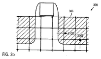
図3bは図3aに示されるデバイス300の断面図を模式的に示しており、キャビティ306はハッチング線を付された区域によって模式的に図示されており、その区域は水平及び垂直な成長方向を規定しており、これらの成長方向は同一のミラー指数によって指定されており、即ち水平及び垂直な成長プロセスに対するそれぞれのテンプレート表面は(100)面であり、それにより、シリコン/ゲルマニウム合金のような歪誘起半導体合金を成長させる場合における従来の技術において生成されるであろうそれぞれの積層障害を低減している。
FIG. 3b schematically shows a cross-sectional view of the
図3cは更なる例示的な実施形態に従う半導体デバイス300を模式的に示しており、この実施形態においては、シリコンのような立方格子に対して<100>方向及び<110>方向が図3cにおいて対応する矢印で示されるように90度の角度オフセットを提示するように、半導体層303が(110)表面方位を呈するように設けられてよい。
FIG. 3c schematically illustrates a
図3dは図3cのデバイスの断面図を模式的に示しており、ここでは(100)は図3dの紙面内に設けられている一方、キャビティ306内のそれぞれの成長方向は<110>方向に基づいている。従って上述したように、シリコン/ゲルマニウム等の歪誘起半導体合金を選択的に成長させる場合には、減少させられた数の積層障害が生成されるであろうから、既に論じられたように、ホウ素のような軽いドーパント種の拡散挙動に関する利益を提供することができる。
FIG. 3d schematically shows a cross-sectional view of the device of FIG. 3c, where (100) is provided in the plane of FIG. 3d, while each growth direction in the
図3eは凹部306内に歪誘起半導体合金を埋めるための対応するエピタキシャル成長プロセス312の間における半導体デバイス300を模式的に示している。プロセス312の間、ゲート電極351A及びゲート絶縁層351Bはキャップ層304及び側壁スペーサ305によって密閉されていてよい。半導体層303の特定の結晶構造により、実質的に垂直な表面306V及び実質的に水平な表面306Hに対して、ミラー指数(hkl)で示される実質的に等価な結晶面が直面するであろう。従って、成長プロセス312の間に生成され得る格子不連続性の程度を低減することができる。
FIG. 3 e schematically illustrates the
図3fは歪誘起半導体合金355を有する半導体デバイス300を模式的に示しており、トランジスタ350がPチャネルトランジスタを代表してよい場合には、歪誘起半導体合金355はシリコン/ゲルマニウム材質を代表してよい。また図示された実施形態においては、追加的に、例えば窒素、炭素、フッ素等の形態にある拡散阻害種356が、後続の焼鈍プロセスの間における拡散不均一性を更に低減するために設けられてよい。1つの実施形態においては、拡散阻害種356は、先行する成長プロセス312の間に大量の格子欠陥が本来的に生成され得る臨界部分355Aに空間的に限定されていてよい。しかし、整合している成長方向<hkl>により(図3e参照)、対応する格子欠陥353Dの数及び寸法は小さくなり得るので、拡散阻害種356の濃度及び/又は局部的拡張の要求を低減することができる。例えば、適度に低い濃度を有する種356を所望の位置に設けるために、例えばエピタキシャル成長プロセス312に先立ち、例えば線量、エネルギー及び傾斜角度に関する適切な注入パラメータに基き拡散阻害種356が導入されてよい。他の場合には、デバイス100及び200を参照して前述してもあるように、カウンタードープ領域(図示せず)もまた形成され得る注入シーケンスの間に、拡散阻害種356がイオン注入によって組み込まれてもよい。他の例示的な実施形態においては、拡散阻害種356は、図2eに示されるのと同様に、更に形成されることになるPN接合の全長に実質的に沿って拡張するように組み込まれてよい。
FIG. 3f schematically illustrates a
従って、欠陥353Dの量を減らすことによって、結果として得られるPN接合の高い均一性を達成することができ、更なる例示的な実施形態においては、拡散阻害種356が少なくとも臨界デバイス区域に、しかし減少された濃度で追加的に設けられてよく、これにより総合的なデバイス特性を考慮した拡散阻害種にの任意の影響を更に低減しながら、全体的なトランジスタの均一性を高めることができる。 Thus, by reducing the amount of defects 353D, high uniformity of the resulting PN junction can be achieved, and in a further exemplary embodiment, the diffusion inhibiting species 356 is at least in the critical device area, but It may additionally be provided at a reduced concentration, thereby increasing the overall transistor uniformity while further reducing any impact on the diffusion-inhibiting species considering the overall device characteristics.
図4を参照して、選択的なエピタキシャル成長プロセスの間に拡散阻害種が少なくとも部分的に組み込まれ得る更なる例示的な実施形態を以下に説明する。 With reference to FIG. 4, further exemplary embodiments are described below in which diffusion-inhibiting species may be at least partially incorporated during the selective epitaxial growth process.
図4は基板401、半導体層403及び、随意的に埋め込み絶縁層402を含む半導体デバイス400の断面図を模式的に示している。また、半導体層403の一部の内部及び上方にトランジスタ450が形成されていてよく、トランジスタ450はゲート電極構造451、ドレイン及びソース領域453を備えていてよく、ドレイン及びソース領域453内には歪誘起半導体材質455が設けられていてよい。例えばトランジスタ450は、半導体合金455としてシリコン/ゲルマニウム合金を備えたPチャネルトランジスタを代表してよい。更に、ドレイン及びソース領域は半導体層403内に形成されていてよく、それにより、歪誘起材質455内に位置する部分453Nを有していてよいPN接合453Pが画定される。また、拡散阻害種456が材質455と半導体層403の材質との間の界面に設けられていてよい。例えば、拡散阻害材質は炭素、窒素等の形態で組み込まれてよい。その結果、焼鈍プロセスを実行する際、拡散阻害材質456は、臨界的角部455Aでのドレイン及びソース領域453のドーパント種の全体的な拡散活性を適切に低下させることができ、それによりPN接合453Pのそれぞれの部分453Nの高い均一性に貢献する。
FIG. 4 schematically illustrates a cross-sectional view of a
図4に示される半導体デバイス400は前述したのと同様なプロセス技術に基いて形成され得るが、対応するエピタキシャル成長プロセスの間、拡散阻害種456は例えば窒素等の形態で組み込まれてよく、このことは堆積環境へそれぞれの先駆体成分を添加することによって達成され得る。次いで、堆積環境中への拡散阻害種の供給が中止されてよく、そして材質455を得るために、十分に確立されたプロセスパラメータに基いて成長プロセスが継続されてよい。その後、最終的に望まれるドーパントプロファイルを得るために、ドレイン及びソース領域453を形成しまた焼鈍シーケンスを実行することによって更なる処理が継続されてよく、種456は、既に論じられもしたように高い全体的な均一性を提供することができる。
The
結果として、本開示は、PN接合での、特に先行する歪誘起半導体合金の形成に起因して高い欠陥密度を呈することのある臨界部分での不均一性に関連する拡散を低減するための、それぞれの焼鈍プロセスの間における適切な条件を提供することによって、Pチャネルトランジスタの挙動のようなトランジスタ特性を高めることができる技術及び半導体デバイスに関連している。この目的のために、拡散阻害種がPN接合に適切に位置させられてよく、顕著でない拡散活性をもたらし得る、ホウ素のようなドーパント種に対する近隣を提供する。他の場合には、それぞれのキャビティ内の垂直及び水平の成長方向を適切に選択することによって、臨界的なデバイス部分での欠陥密度を低減することができ、このことは拡散阻害種の導入によって支援され得るが、拡散阻害種は低減された濃度で設けられてよく、それにより総合的なトランジスタ特性に対する拡散阻害種の任意の影響を低減することもできる。ここに開示される原理により、ゲート電極構造に隣接するキャビティを形成するためのプロセスシーケンスは、結晶学的に等方的なエッチング技術、例えば空間的な異方性又は等方性を伴うプラズマベースのエッチングプロセスに基いて実行することができ、それにより歪誘起半導体合金の寸法及び形状を調節する上での高い柔軟性を提供することができる。 As a result, the present disclosure is intended to reduce diffusion associated with non-uniformities at critical portions that may exhibit high defect density due to the formation of a prior strain-induced semiconductor alloy, particularly at a PN junction. It relates to technologies and semiconductor devices that can enhance transistor characteristics, such as the behavior of P-channel transistors, by providing appropriate conditions during each annealing process. For this purpose, diffusion-inhibiting species can be properly located at the PN junction, providing a neighborhood for dopant species such as boron that can result in inconspicuous diffusion activity. In other cases, by properly selecting the vertical and horizontal growth directions within each cavity, the defect density in critical device parts can be reduced, which is due to the introduction of diffusion-inhibiting species. Although supported, the diffusion-inhibiting species may be provided at a reduced concentration, thereby reducing any effect of the diffusion-inhibiting species on the overall transistor characteristics. In accordance with the principles disclosed herein, the process sequence for forming the cavity adjacent to the gate electrode structure is based on a crystallographically isotropic etching technique such as a plasma-based with spatial anisotropy or isotropic property. Can be performed on the basis of the etching process, which can provide a high degree of flexibility in adjusting the size and shape of the strain-inducing semiconductor alloy.
以上開示された特定の実施形態は例示にすぎず、本発明は修正されてよく、また、ここでの教示の利益を享受する当業者に明らかな、均等であるが異なるやり方で実施されてよい。例えば、上述したプロセスステップは異なる順序で実行されてよい。また、以下の特許請求の範囲に記載されていることを除き、ここで示されている構成又は設計の詳細に限定することは意図されていない。従って、以上開示された特定の実施形態が変更され又は修正されてよく、そのような全ての変形が本発明の精神及び範囲内にあるものとみなされることは明らかである。従って、ここでの保護の対象は以下の特許請求の範囲に記載された通りである。 The specific embodiments disclosed above are merely exemplary and the invention may be modified and implemented in an equivalent but different manner apparent to those of ordinary skill in the art having the benefit of the teachings herein. . For example, the process steps described above may be performed in a different order. It is not intended to be limited to the details of construction or design shown herein other than as described in the claims below. It is therefore evident that the particular embodiments disclosed above may be altered or modified and all such variations are considered within the spirit and scope of the invention. Accordingly, the subject of protection herein is as set forth in the following claims.
Claims (16)
前記アクティブ半導体領域(203A)内の拡散阻害種(256A)を前記ドレイン及びソース領域(253)によって形成されるPN接合の少なくとも一部分に対応する空間的に制限された区域に位置させることと、
前記ドレイン及びソース領域(253)内のドーパントを活性化させるために前記ドレイン及びソース領域(253)を焼鈍することとを備えた方法。 Forming a drain and source region (253) of the field effect transistor (250) in the active semiconductor region (203A), the drain and source region (253) having a strain-inducing semiconductor alloy (255);
Positioning the diffusion inhibiting species (256A) in the active semiconductor region (203A) in a spatially confined area corresponding to at least a portion of a PN junction formed by the drain and source regions (253);
Annealing the drain and source regions (253) to activate dopants in the drain and source regions (253).
前記キャビティ(306)内に歪誘起半導体合金(355)を形成することと、
前記ゲート電極構造(351A)に隣接して前記半導体領域(303)内にドレイン及びソース領域を形成することとを備えた方法であって、
前記結晶性の半導体領域は立方格子構造を備えており、前記キャビティ(306)は前記結晶性の半導体領域の表面方位によって規定される第2の結晶方向と実質的に等価な第1の結晶方向に対応する長さ方向を規定している方法。 Forming a cavity (306) in the crystalline semiconductor region (303) adjacent to a gate electrode structure (351A) formed above a portion of the crystalline semiconductor region (303);
Forming a strain-inducing semiconductor alloy (355) in the cavity (306);
Forming a drain and source region in the semiconductor region (303) adjacent to the gate electrode structure (351A), comprising:
The crystalline semiconductor region has a cubic lattice structure, and the cavity (306) has a first crystal direction substantially equivalent to a second crystal direction defined by a surface orientation of the crystalline semiconductor region. A method that specifies the length direction corresponding to.
ドーパント種としてのホウ素に基くアクティブ領域内に形成され、前記トランジスタ(250)のチャネル領域と共にPN接合を形成し、歪誘起半導体合金(255)を含むドレイン及びソース領域(253)と、
前記PN接合の少なくとも一部に沿って位置されられる非ドープの拡散阻害種(256A)とを備えている半導体デバイス。 A semiconductor device comprising a transistor (250) formed above a substrate, the transistor comprising:
A drain and source region (253) formed in an active region based on boron as a dopant species, forming a PN junction with the channel region of the transistor (250), and comprising a strain-inducing semiconductor alloy (255);
A semiconductor device comprising: an undoped diffusion inhibiting species (256A) located along at least a portion of the PN junction.
Applications Claiming Priority (5)
| Application Number | Priority Date | Filing Date | Title |
|---|---|---|---|
| DE102008035806.1 | 2008-07-31 | ||
| DE102008035806A DE102008035806B4 (en) | 2008-07-31 | 2008-07-31 | Process for manufacturing a semiconductor device or a transistor with embedded Si / GE material with improved boron inclusion and transistor |
| US12/503,340 | 2009-07-15 | ||
| US12/503,340 US20100025743A1 (en) | 2008-07-31 | 2009-07-15 | Transistor with embedded si/ge material having enhanced boron confinement |
| PCT/US2009/004425 WO2010014251A2 (en) | 2008-07-31 | 2009-07-31 | Transistor with embedded si/ge material having enhanced boron confinement |
Publications (2)
| Publication Number | Publication Date |
|---|---|
| JP2011530167A true JP2011530167A (en) | 2011-12-15 |
| JP2011530167A5 JP2011530167A5 (en) | 2012-09-06 |
Family
ID=41461560
Family Applications (1)
| Application Number | Title | Priority Date | Filing Date |
|---|---|---|---|
| JP2011521127A Pending JP2011530167A (en) | 2008-07-31 | 2009-07-31 | Transistor with embedded Si / Ge material with enhanced boron confinement |
Country Status (8)
| Country | Link |
|---|---|
| US (1) | US20100025743A1 (en) |
| JP (1) | JP2011530167A (en) |
| KR (1) | KR20110046501A (en) |
| CN (1) | CN102105965A (en) |
| DE (1) | DE102008035806B4 (en) |
| GB (1) | GB2474170B (en) |
| TW (1) | TW201017773A (en) |
| WO (1) | WO2010014251A2 (en) |
Cited By (1)
| Publication number | Priority date | Publication date | Assignee | Title |
|---|---|---|---|---|
| JP2020031170A (en) * | 2018-08-24 | 2020-02-27 | キオクシア株式会社 | Semiconductor device |
Families Citing this family (12)
| Publication number | Priority date | Publication date | Assignee | Title |
|---|---|---|---|---|
| US20110012177A1 (en) * | 2009-07-20 | 2011-01-20 | International Business Machines Corporation | Nanostructure For Changing Electric Mobility |
| US8368125B2 (en) * | 2009-07-20 | 2013-02-05 | International Business Machines Corporation | Multiple orientation nanowires with gate stack stressors |
| KR20120107762A (en) * | 2011-03-22 | 2012-10-04 | 삼성전자주식회사 | Methods of fabricating semiconductor devices |
| US9263342B2 (en) * | 2012-03-02 | 2016-02-16 | Taiwan Semiconductor Manufacturing Company, Ltd. | Semiconductor device having a strained region |
| US8674447B2 (en) | 2012-04-27 | 2014-03-18 | International Business Machines Corporation | Transistor with improved sigma-shaped embedded stressor and method of formation |
| US9165944B2 (en) | 2013-10-07 | 2015-10-20 | Globalfoundries Inc. | Semiconductor device including SOI butted junction to reduce short-channel penalty |
| US10153371B2 (en) | 2014-02-07 | 2018-12-11 | Stmicroelectronics, Inc. | Semiconductor device with fins including sidewall recesses |
| US9190516B2 (en) * | 2014-02-21 | 2015-11-17 | Globalfoundries Inc. | Method for a uniform compressive strain layer and device thereof |
| US9190418B2 (en) | 2014-03-18 | 2015-11-17 | Globalfoundries U.S. 2 Llc | Junction butting in SOI transistor with embedded source/drain |
| US9466718B2 (en) | 2014-03-31 | 2016-10-11 | Stmicroelectronics, Inc. | Semiconductor device with fin and related methods |
| US10008568B2 (en) | 2015-03-30 | 2018-06-26 | Taiwan Semiconductor Manufacturing Co., Ltd. | Structure and formation method of semiconductor device structure |
| US9741853B2 (en) * | 2015-10-29 | 2017-08-22 | Globalfoundries Inc. | Stress memorization techniques for transistor devices |
Citations (5)
| Publication number | Priority date | Publication date | Assignee | Title |
|---|---|---|---|---|
| JP2002057118A (en) * | 2000-08-09 | 2002-02-22 | Toshiba Corp | Semiconductor device and its manufacturing method |
| JP2006013428A (en) * | 2004-05-26 | 2006-01-12 | Fujitsu Ltd | Manufacturing method of semiconductor device |
| JP2006013082A (en) * | 2004-06-24 | 2006-01-12 | Fujitsu Ltd | Semiconductor apparatus and manufacturing method thereof, and method of evaluating semiconductor apparatus |
| JP2006059843A (en) * | 2004-08-17 | 2006-03-02 | Toshiba Corp | Semiconductor device and its manufacturing method |
| US20090026552A1 (en) * | 2007-07-27 | 2009-01-29 | Da Zhang | Method for forming a transistor having gate dielectric protection and structure |
Family Cites Families (19)
| Publication number | Priority date | Publication date | Assignee | Title |
|---|---|---|---|---|
| US5770485A (en) * | 1997-03-04 | 1998-06-23 | Advanced Micro Devices, Inc. | MOSFET device with an amorphized source and fabrication method thereof |
| JPH10308361A (en) * | 1997-05-07 | 1998-11-17 | Mitsubishi Electric Corp | Semiconductor device and manufacture of the same |
| US5877056A (en) * | 1998-01-08 | 1999-03-02 | Texas Instruments-Acer Incorporated | Ultra-short channel recessed gate MOSFET with a buried contact |
| US6580639B1 (en) * | 1999-08-10 | 2003-06-17 | Advanced Micro Devices, Inc. | Method of reducing program disturbs in NAND type flash memory devices |
| US6657223B1 (en) * | 2002-10-29 | 2003-12-02 | Advanced Micro Devices, Inc. | Strained silicon MOSFET having silicon source/drain regions and method for its fabrication |
| KR100588786B1 (en) * | 2003-09-18 | 2006-06-12 | 동부일렉트로닉스 주식회사 | Fabricating method of semiconductor device |
| US7314804B2 (en) * | 2005-01-04 | 2008-01-01 | Intel Corporation | Plasma implantation of impurities in junction region recesses |
| US7407850B2 (en) * | 2005-03-29 | 2008-08-05 | Texas Instruments Incorporated | N+ poly on high-k dielectric for semiconductor devices |
| US7892905B2 (en) * | 2005-08-02 | 2011-02-22 | Globalfoundries Singapore Pte. Ltd. | Formation of strained Si channel and Si1-xGex source/drain structures using laser annealing |
| US7612421B2 (en) * | 2005-10-11 | 2009-11-03 | Atmel Corporation | Electronic device with dopant diffusion barrier and tunable work function and methods of making same |
| DE102005052055B3 (en) * | 2005-10-31 | 2007-04-26 | Advanced Micro Devices, Inc., Sunnyvale | Transistor and semiconductor components and production process for thin film silicon on insulator transistor has embedded deformed layer |
| US7608515B2 (en) * | 2006-02-14 | 2009-10-27 | Taiwan Semiconductor Manufacturing Company, Ltd. | Diffusion layer for stressed semiconductor devices |
| US7364976B2 (en) * | 2006-03-21 | 2008-04-29 | Intel Corporation | Selective etch for patterning a semiconductor film deposited non-selectively |
| DE102006019835B4 (en) * | 2006-04-28 | 2011-05-12 | Advanced Micro Devices, Inc., Sunnyvale | Transistor having a channel with tensile strain oriented along a crystallographic orientation with increased charge carrier mobility |
| DE102006030261B4 (en) * | 2006-06-30 | 2011-01-20 | Advanced Micro Devices, Inc., Sunnyvale | A method of fabricating a drain / source extension structure of a reduced boron diffusion transistor field effect transistor |
| DE102006035669B4 (en) * | 2006-07-31 | 2014-07-10 | Globalfoundries Inc. | Transistor having a deformed channel region having a performance enhancing material composition and methods of manufacture |
| US7625801B2 (en) * | 2006-09-19 | 2009-12-01 | Taiwan Semiconductor Manufacturing Company, Ltd. | Silicide formation with a pre-amorphous implant |
| DE102006046363B4 (en) * | 2006-09-29 | 2009-04-16 | Advanced Micro Devices, Inc., Sunnyvale | A method for reducing crystal defects in reshuffled shallow junction transistors by appropriately selecting crystal orientations |
| DE102007030053B4 (en) * | 2007-06-29 | 2011-07-21 | Advanced Micro Devices, Inc., Calif. | Reduce pn junction capacitance in a transistor by lowering drain and source regions |
-
2008
- 2008-07-31 DE DE102008035806A patent/DE102008035806B4/en active Active
-
2009
- 2009-07-15 US US12/503,340 patent/US20100025743A1/en not_active Abandoned
- 2009-07-30 TW TW098125630A patent/TW201017773A/en unknown
- 2009-07-31 JP JP2011521127A patent/JP2011530167A/en active Pending
- 2009-07-31 CN CN2009801291552A patent/CN102105965A/en active Pending
- 2009-07-31 GB GB1100855.4A patent/GB2474170B/en active Active
- 2009-07-31 KR KR1020117004347A patent/KR20110046501A/en not_active Application Discontinuation
- 2009-07-31 WO PCT/US2009/004425 patent/WO2010014251A2/en active Application Filing
Patent Citations (5)
| Publication number | Priority date | Publication date | Assignee | Title |
|---|---|---|---|---|
| JP2002057118A (en) * | 2000-08-09 | 2002-02-22 | Toshiba Corp | Semiconductor device and its manufacturing method |
| JP2006013428A (en) * | 2004-05-26 | 2006-01-12 | Fujitsu Ltd | Manufacturing method of semiconductor device |
| JP2006013082A (en) * | 2004-06-24 | 2006-01-12 | Fujitsu Ltd | Semiconductor apparatus and manufacturing method thereof, and method of evaluating semiconductor apparatus |
| JP2006059843A (en) * | 2004-08-17 | 2006-03-02 | Toshiba Corp | Semiconductor device and its manufacturing method |
| US20090026552A1 (en) * | 2007-07-27 | 2009-01-29 | Da Zhang | Method for forming a transistor having gate dielectric protection and structure |
Cited By (2)
| Publication number | Priority date | Publication date | Assignee | Title |
|---|---|---|---|---|
| JP2020031170A (en) * | 2018-08-24 | 2020-02-27 | キオクシア株式会社 | Semiconductor device |
| JP7150524B2 (en) | 2018-08-24 | 2022-10-11 | キオクシア株式会社 | semiconductor equipment |
Also Published As
| Publication number | Publication date |
|---|---|
| CN102105965A (en) | 2011-06-22 |
| US20100025743A1 (en) | 2010-02-04 |
| KR20110046501A (en) | 2011-05-04 |
| DE102008035806B4 (en) | 2010-06-10 |
| WO2010014251A2 (en) | 2010-02-04 |
| DE102008035806A1 (en) | 2010-02-04 |
| WO2010014251A3 (en) | 2010-04-08 |
| GB2474170B (en) | 2012-08-22 |
| GB2474170A (en) | 2011-04-06 |
| GB201100855D0 (en) | 2011-03-02 |
| TW201017773A (en) | 2010-05-01 |
Similar Documents
| Publication | Publication Date | Title |
|---|---|---|
| JP2011530167A (en) | Transistor with embedded Si / Ge material with enhanced boron confinement | |
| TWI387009B (en) | Technique for reducing crystal defects in strained transistors by tilted preamorphization | |
| JP5795260B2 (en) | Transistor with embedded strain-inducing material having a step-shaped structure | |
| US8138050B2 (en) | Transistor device comprising an asymmetric embedded semiconductor alloy | |
| KR101605150B1 (en) | In situ formed drain and source regions including a strain inducing alloy and a graded dopant profile | |
| US8093634B2 (en) | In situ formed drain and source regions in a silicon/germanium containing transistor device | |
| US7208397B2 (en) | Transistor having an asymmetric source/drain and halo implantation region and a method of forming the same | |
| US8039878B2 (en) | Transistor having a channel with tensile strain and oriented along a crystallographic orientation with increased charge carrier mobility | |
| US9041126B2 (en) | Deeply depleted MOS transistors having a screening layer and methods thereof | |
| US8338274B2 (en) | Transistor device comprising an embedded semiconductor alloy having an asymmetric configuration | |
| US8664056B2 (en) | Transistor with embedded strain-inducing material formed in diamond-shaped cavities based on a pre-amorphization | |
| JP5614184B2 (en) | Manufacturing method of semiconductor device | |
| JP2009528698A (en) | Transistor device that further stabilizes threshold without reducing drive current | |
| US7939399B2 (en) | Semiconductor device having a strained semiconductor alloy concentration profile | |
| TWI556320B (en) | Low thermal budget schemes in semiconductor device fabrication | |
| US20090250771A1 (en) | Mosfet and production method of semiconductor device | |
| KR100574172B1 (en) | Method for fabricating semiconductor device | |
| US8377781B2 (en) | Transistor with asymmetric silicon germanium source region | |
| US8951877B2 (en) | Transistor with embedded strain-inducing material formed in cavities based on an amorphization process and a heat treatment | |
| WO2007130240A1 (en) | A transistor having a channel with tensile strain and oriented along a crystallographic orientation with increased charge carrier mobility |
Legal Events
| Date | Code | Title | Description |
|---|---|---|---|
| A521 | Written amendment |
Free format text: JAPANESE INTERMEDIATE CODE: A523 Effective date: 20120719 |
|
| A621 | Written request for application examination |
Free format text: JAPANESE INTERMEDIATE CODE: A621 Effective date: 20120719 |
|
| A977 | Report on retrieval |
Free format text: JAPANESE INTERMEDIATE CODE: A971007 Effective date: 20131216 |
|
| A131 | Notification of reasons for refusal |
Free format text: JAPANESE INTERMEDIATE CODE: A131 Effective date: 20140129 |
|
| A02 | Decision of refusal |
Free format text: JAPANESE INTERMEDIATE CODE: A02 Effective date: 20140625 |