JP2011523910A - Next generation screen printing system - Google Patents
Next generation screen printing system Download PDFInfo
- Publication number
- JP2011523910A JP2011523910A JP2011509948A JP2011509948A JP2011523910A JP 2011523910 A JP2011523910 A JP 2011523910A JP 2011509948 A JP2011509948 A JP 2011509948A JP 2011509948 A JP2011509948 A JP 2011509948A JP 2011523910 A JP2011523910 A JP 2011523910A
- Authority
- JP
- Japan
- Prior art keywords
- substrate
- conveyor
- rotary actuator
- substrate support
- support
- Prior art date
- Legal status (The legal status is an assumption and is not a legal conclusion. Google has not performed a legal analysis and makes no representation as to the accuracy of the status listed.)
- Pending
Links
Images


Classifications
-
- H—ELECTRICITY
- H01—ELECTRIC ELEMENTS
- H01L—SEMICONDUCTOR DEVICES NOT COVERED BY CLASS H10
- H01L21/00—Processes or apparatus adapted for the manufacture or treatment of semiconductor or solid state devices or of parts thereof
- H01L21/67—Apparatus specially adapted for handling semiconductor or electric solid state devices during manufacture or treatment thereof; Apparatus specially adapted for handling wafers during manufacture or treatment of semiconductor or electric solid state devices or components ; Apparatus not specifically provided for elsewhere
- H01L21/677—Apparatus specially adapted for handling semiconductor or electric solid state devices during manufacture or treatment thereof; Apparatus specially adapted for handling wafers during manufacture or treatment of semiconductor or electric solid state devices or components ; Apparatus not specifically provided for elsewhere for conveying, e.g. between different workstations
- H01L21/67703—Apparatus specially adapted for handling semiconductor or electric solid state devices during manufacture or treatment thereof; Apparatus specially adapted for handling wafers during manufacture or treatment of semiconductor or electric solid state devices or components ; Apparatus not specifically provided for elsewhere for conveying, e.g. between different workstations between different workstations
- H01L21/67715—Changing the direction of the conveying path
-
- H—ELECTRICITY
- H01—ELECTRIC ELEMENTS
- H01L—SEMICONDUCTOR DEVICES NOT COVERED BY CLASS H10
- H01L21/00—Processes or apparatus adapted for the manufacture or treatment of semiconductor or solid state devices or of parts thereof
- H01L21/67—Apparatus specially adapted for handling semiconductor or electric solid state devices during manufacture or treatment thereof; Apparatus specially adapted for handling wafers during manufacture or treatment of semiconductor or electric solid state devices or components ; Apparatus not specifically provided for elsewhere
- H01L21/67005—Apparatus not specifically provided for elsewhere
- H01L21/67011—Apparatus for manufacture or treatment
- H01L21/67155—Apparatus for manufacturing or treating in a plurality of work-stations
- H01L21/67207—Apparatus for manufacturing or treating in a plurality of work-stations comprising a chamber adapted to a particular process
- H01L21/6723—Apparatus for manufacturing or treating in a plurality of work-stations comprising a chamber adapted to a particular process comprising at least one plating chamber
-
- C—CHEMISTRY; METALLURGY
- C23—COATING METALLIC MATERIAL; COATING MATERIAL WITH METALLIC MATERIAL; CHEMICAL SURFACE TREATMENT; DIFFUSION TREATMENT OF METALLIC MATERIAL; COATING BY VACUUM EVAPORATION, BY SPUTTERING, BY ION IMPLANTATION OR BY CHEMICAL VAPOUR DEPOSITION, IN GENERAL; INHIBITING CORROSION OF METALLIC MATERIAL OR INCRUSTATION IN GENERAL
- C23C—COATING METALLIC MATERIAL; COATING MATERIAL WITH METALLIC MATERIAL; SURFACE TREATMENT OF METALLIC MATERIAL BY DIFFUSION INTO THE SURFACE, BY CHEMICAL CONVERSION OR SUBSTITUTION; COATING BY VACUUM EVAPORATION, BY SPUTTERING, BY ION IMPLANTATION OR BY CHEMICAL VAPOUR DEPOSITION, IN GENERAL
- C23C16/00—Chemical coating by decomposition of gaseous compounds, without leaving reaction products of surface material in the coating, i.e. chemical vapour deposition [CVD] processes
- C23C16/44—Chemical coating by decomposition of gaseous compounds, without leaving reaction products of surface material in the coating, i.e. chemical vapour deposition [CVD] processes characterised by the method of coating
- C23C16/458—Chemical coating by decomposition of gaseous compounds, without leaving reaction products of surface material in the coating, i.e. chemical vapour deposition [CVD] processes characterised by the method of coating characterised by the method used for supporting substrates in the reaction chamber
-
- H—ELECTRICITY
- H01—ELECTRIC ELEMENTS
- H01L—SEMICONDUCTOR DEVICES NOT COVERED BY CLASS H10
- H01L21/00—Processes or apparatus adapted for the manufacture or treatment of semiconductor or solid state devices or of parts thereof
- H01L21/67—Apparatus specially adapted for handling semiconductor or electric solid state devices during manufacture or treatment thereof; Apparatus specially adapted for handling wafers during manufacture or treatment of semiconductor or electric solid state devices or components ; Apparatus not specifically provided for elsewhere
- H01L21/677—Apparatus specially adapted for handling semiconductor or electric solid state devices during manufacture or treatment thereof; Apparatus specially adapted for handling wafers during manufacture or treatment of semiconductor or electric solid state devices or components ; Apparatus not specifically provided for elsewhere for conveying, e.g. between different workstations
- H01L21/67703—Apparatus specially adapted for handling semiconductor or electric solid state devices during manufacture or treatment thereof; Apparatus specially adapted for handling wafers during manufacture or treatment of semiconductor or electric solid state devices or components ; Apparatus not specifically provided for elsewhere for conveying, e.g. between different workstations between different workstations
- H01L21/67721—Apparatus specially adapted for handling semiconductor or electric solid state devices during manufacture or treatment thereof; Apparatus specially adapted for handling wafers during manufacture or treatment of semiconductor or electric solid state devices or components ; Apparatus not specifically provided for elsewhere for conveying, e.g. between different workstations between different workstations the substrates to be conveyed not being semiconductor wafers or large planar substrates, e.g. chips, lead frames
-
- H—ELECTRICITY
- H01—ELECTRIC ELEMENTS
- H01L—SEMICONDUCTOR DEVICES NOT COVERED BY CLASS H10
- H01L21/00—Processes or apparatus adapted for the manufacture or treatment of semiconductor or solid state devices or of parts thereof
- H01L21/67—Apparatus specially adapted for handling semiconductor or electric solid state devices during manufacture or treatment thereof; Apparatus specially adapted for handling wafers during manufacture or treatment of semiconductor or electric solid state devices or components ; Apparatus not specifically provided for elsewhere
- H01L21/677—Apparatus specially adapted for handling semiconductor or electric solid state devices during manufacture or treatment thereof; Apparatus specially adapted for handling wafers during manufacture or treatment of semiconductor or electric solid state devices or components ; Apparatus not specifically provided for elsewhere for conveying, e.g. between different workstations
- H01L21/67739—Apparatus specially adapted for handling semiconductor or electric solid state devices during manufacture or treatment thereof; Apparatus specially adapted for handling wafers during manufacture or treatment of semiconductor or electric solid state devices or components ; Apparatus not specifically provided for elsewhere for conveying, e.g. between different workstations into and out of processing chamber
- H01L21/67748—Apparatus specially adapted for handling semiconductor or electric solid state devices during manufacture or treatment thereof; Apparatus specially adapted for handling wafers during manufacture or treatment of semiconductor or electric solid state devices or components ; Apparatus not specifically provided for elsewhere for conveying, e.g. between different workstations into and out of processing chamber horizontal transfer of a single workpiece
-
- H—ELECTRICITY
- H01—ELECTRIC ELEMENTS
- H01L—SEMICONDUCTOR DEVICES NOT COVERED BY CLASS H10
- H01L21/00—Processes or apparatus adapted for the manufacture or treatment of semiconductor or solid state devices or of parts thereof
- H01L21/67—Apparatus specially adapted for handling semiconductor or electric solid state devices during manufacture or treatment thereof; Apparatus specially adapted for handling wafers during manufacture or treatment of semiconductor or electric solid state devices or components ; Apparatus not specifically provided for elsewhere
- H01L21/677—Apparatus specially adapted for handling semiconductor or electric solid state devices during manufacture or treatment thereof; Apparatus specially adapted for handling wafers during manufacture or treatment of semiconductor or electric solid state devices or components ; Apparatus not specifically provided for elsewhere for conveying, e.g. between different workstations
- H01L21/67739—Apparatus specially adapted for handling semiconductor or electric solid state devices during manufacture or treatment thereof; Apparatus specially adapted for handling wafers during manufacture or treatment of semiconductor or electric solid state devices or components ; Apparatus not specifically provided for elsewhere for conveying, e.g. between different workstations into and out of processing chamber
- H01L21/6776—Continuous loading and unloading into and out of a processing chamber, e.g. transporting belts within processing chambers
-
- H—ELECTRICITY
- H01—ELECTRIC ELEMENTS
- H01L—SEMICONDUCTOR DEVICES NOT COVERED BY CLASS H10
- H01L21/00—Processes or apparatus adapted for the manufacture or treatment of semiconductor or solid state devices or of parts thereof
- H01L21/67—Apparatus specially adapted for handling semiconductor or electric solid state devices during manufacture or treatment thereof; Apparatus specially adapted for handling wafers during manufacture or treatment of semiconductor or electric solid state devices or components ; Apparatus not specifically provided for elsewhere
- H01L21/683—Apparatus specially adapted for handling semiconductor or electric solid state devices during manufacture or treatment thereof; Apparatus specially adapted for handling wafers during manufacture or treatment of semiconductor or electric solid state devices or components ; Apparatus not specifically provided for elsewhere for supporting or gripping
- H01L21/687—Apparatus specially adapted for handling semiconductor or electric solid state devices during manufacture or treatment thereof; Apparatus specially adapted for handling wafers during manufacture or treatment of semiconductor or electric solid state devices or components ; Apparatus not specifically provided for elsewhere for supporting or gripping using mechanical means, e.g. chucks, clamps or pinches
- H01L21/68714—Apparatus specially adapted for handling semiconductor or electric solid state devices during manufacture or treatment thereof; Apparatus specially adapted for handling wafers during manufacture or treatment of semiconductor or electric solid state devices or components ; Apparatus not specifically provided for elsewhere for supporting or gripping using mechanical means, e.g. chucks, clamps or pinches the wafers being placed on a susceptor, stage or support
- H01L21/68764—Apparatus specially adapted for handling semiconductor or electric solid state devices during manufacture or treatment thereof; Apparatus specially adapted for handling wafers during manufacture or treatment of semiconductor or electric solid state devices or components ; Apparatus not specifically provided for elsewhere for supporting or gripping using mechanical means, e.g. chucks, clamps or pinches the wafers being placed on a susceptor, stage or support characterised by a movable susceptor, stage or support, others than those only rotating on their own vertical axis, e.g. susceptors on a rotating caroussel
-
- H—ELECTRICITY
- H01—ELECTRIC ELEMENTS
- H01L—SEMICONDUCTOR DEVICES NOT COVERED BY CLASS H10
- H01L21/00—Processes or apparatus adapted for the manufacture or treatment of semiconductor or solid state devices or of parts thereof
- H01L21/67—Apparatus specially adapted for handling semiconductor or electric solid state devices during manufacture or treatment thereof; Apparatus specially adapted for handling wafers during manufacture or treatment of semiconductor or electric solid state devices or components ; Apparatus not specifically provided for elsewhere
- H01L21/683—Apparatus specially adapted for handling semiconductor or electric solid state devices during manufacture or treatment thereof; Apparatus specially adapted for handling wafers during manufacture or treatment of semiconductor or electric solid state devices or components ; Apparatus not specifically provided for elsewhere for supporting or gripping
- H01L21/687—Apparatus specially adapted for handling semiconductor or electric solid state devices during manufacture or treatment thereof; Apparatus specially adapted for handling wafers during manufacture or treatment of semiconductor or electric solid state devices or components ; Apparatus not specifically provided for elsewhere for supporting or gripping using mechanical means, e.g. chucks, clamps or pinches
- H01L21/68714—Apparatus specially adapted for handling semiconductor or electric solid state devices during manufacture or treatment thereof; Apparatus specially adapted for handling wafers during manufacture or treatment of semiconductor or electric solid state devices or components ; Apparatus not specifically provided for elsewhere for supporting or gripping using mechanical means, e.g. chucks, clamps or pinches the wafers being placed on a susceptor, stage or support
- H01L21/68771—Apparatus specially adapted for handling semiconductor or electric solid state devices during manufacture or treatment thereof; Apparatus specially adapted for handling wafers during manufacture or treatment of semiconductor or electric solid state devices or components ; Apparatus not specifically provided for elsewhere for supporting or gripping using mechanical means, e.g. chucks, clamps or pinches the wafers being placed on a susceptor, stage or support characterised by supporting more than one semiconductor substrate
Abstract
本発明の実施形態は、より高いシステムスループット、改善されたシステム動作可能時間及び改善されたデバイス歩留まり性能を有する多重スクリーン印刷チャンバ処理システムを使用して、処理済みの基板での再現性があり且つ正確なスクリーン印刷処理を維持しながら基板を処理するための装置及び方法を提供する。一実施形態において、多重スクリーン印刷チャンバ処理システムは、結晶シリコン太陽電池製造ラインの一部においてスクリーン印刷処理を実行するように構成されており、この製造ラインにおいて、基板は所望の材料でパターン化され、次に続く1つ以上の処理チャンバにおいて処理される。 Embodiments of the present invention are reproducible on processed substrates using a multi-screen printing chamber processing system with higher system throughput, improved system uptime and improved device yield performance, and An apparatus and method for processing a substrate while maintaining an accurate screen printing process is provided. In one embodiment, the multiple screen printing chamber processing system is configured to perform a screen printing process in a portion of a crystalline silicon solar cell production line, where the substrate is patterned with a desired material. Are processed in one or more subsequent processing chambers.
Description
(発明の分野)
本発明は、スクリーン印刷法を利用して基板の表面にパターン層を堆積する際に使用するシステムに関する。
(Field of Invention)
The present invention relates to a system for use in depositing a pattern layer on a surface of a substrate using a screen printing method.
(背景技術の説明)
太陽電池は、太陽光を直接、電力に変換する光起電(PV)装置である。太陽電池は、典型的には、1つ以上のp−n接合を有する。各接合は半導体材料内に2つの異なる領域を有し、一方はpタイプ領域、もう一方はnタイプ領域と称される。太陽電池のp−n接合を太陽光(光子からのエネルギーから成る)に暴露すると、太陽光がPV作用により直接、電気に変換される。太陽電池は特定量の電力を発生し、また所望の量のシステム電力を供給するサイズに設計されたモジュール状に敷設される。太陽電池モジュールは、特殊なフレーム及びコネクタを使用してパネル状に接合される。太陽電池は一般にシリコン基板上に形成され、このシリコン基板は単結晶シリコン又は多結晶シリコン基板である。典型的な太陽電池は、pタイプ領域の上にnタイプシリコンの薄層が形成された、典型的には厚さ約0.3mm未満のシリコンウェハ、基板又はシートを含む。
(Description of background technology)
A solar cell is a photovoltaic (PV) device that converts sunlight directly into electrical power. Solar cells typically have one or more pn junctions. Each junction has two different regions in the semiconductor material, one called a p-type region and the other an n-type region. When the pn junction of a solar cell is exposed to sunlight (consisting of energy from photons), the sunlight is converted directly into electricity by the PV action. Solar cells generate a specific amount of power and are laid out in modules designed to be sized to supply the desired amount of system power. The solar cell module is joined in a panel shape using a special frame and connector. Solar cells are generally formed on a silicon substrate, which is a single crystal silicon or polycrystalline silicon substrate. A typical solar cell comprises a silicon wafer, substrate or sheet, typically less than about 0.3 mm thick, with a thin layer of n-type silicon formed over the p-type region.
この10年の間、PV市場は30%を越える年間成長率の成長を遂げている。太陽電池による発電量が近い将来に世界レベルに10GWpを越える可能性があると示唆する記事もある。全体の95%を越える太陽電池モジュールがシリコンウェハ系であると推定されている。市場における高い成長率に、太陽電池による発電コストを大幅に削減する必要性が加わり、高品質の太陽電池を安価に形成する多数の試みが懸命になされてきた。従って、商業的に実現可能な太陽電池の製造においては、デバイス歩留まりの改善及び基板スループットの上昇によって、太陽電池の形成に必要な製造コストを削減することが1つの大きなポイントとなる。 During the last decade, the PV market has grown at an annual rate of over 30%. Some articles suggest that the amount of power generated by solar cells may exceed 10 GWp on a world level in the near future. It is estimated that more than 95% of the total solar cell modules are based on silicon wafers. With the high growth rate in the market added to the need to significantly reduce the cost of power generation by solar cells, numerous attempts have been made to form high quality solar cells at low cost. Therefore, in the manufacture of commercially viable solar cells, one major point is to reduce the manufacturing cost required for forming the solar cells by improving the device yield and increasing the substrate throughput.
スクリーン印刷は、模様を物体(布等)上に印刷するのに長く使用されてきており、またエレクトロニクス産業では、電子部品の模様(電気接点、相互接続部等)を基板の表面上に印刷するのに使用されている。最先端の太陽電池製造方法でも、スクリーン印刷法が使用されている。 Screen printing has long been used to print patterns on objects (cloth, etc.), and in the electronics industry, patterns of electronic components (electrical contacts, interconnects, etc.) are printed on the surface of a substrate. Is used. Screen printing is also used in the most advanced solar cell manufacturing methods.
従って、既知の装置より高いスループット及びより低い所有コストの太陽電池、電子回路又はその他の有用なデバイスを製造するためのスクリーン印刷装置が必要とされている。 Accordingly, there is a need for a screen printing apparatus for producing solar cells, electronic circuits or other useful devices that have higher throughput and lower cost of ownership than known equipment.
本発明の実施形態は基板表面上にパターン材料を堆積するための装置を提供し、本装置は、回転軸を有する回転アクチュエータと、この回転アクチュエータにそれぞれ連結された第1基板支持体及び第2基板支持体と、回転アクチュエータが第1方向に角度をなして位置決めされた場合に基板を第1基板支持体に搬送するように位置決めされた第1コンベヤと、回転アクチュエータが第1方向に角度をなして位置決めされた場合に基板を第1基板支持体から受け取るように位置決めされた第2コンベヤと、回転アクチュエータが第1方向に角度をなして位置決めされた場合に基板を第2基板支持体に搬送するように位置決めされた第3コンベヤと、回転アクチュエータが第1方向に角度をなして位置決めされた場合に基板を第2基板支持体から受け取るように位置決めされた第4コンベヤとを備える。 Embodiments of the present invention provide an apparatus for depositing pattern material on a substrate surface, the apparatus comprising a rotary actuator having a rotation axis, a first substrate support and a second substrate respectively coupled to the rotation actuator. A substrate support, a first conveyor positioned to transport the substrate to the first substrate support when the rotary actuator is positioned at an angle in the first direction, and the rotary actuator angled in the first direction. A second conveyor positioned to receive the substrate from the first substrate support when positioned, and a substrate to the second substrate support when the rotary actuator is positioned at an angle in the first direction. A third conveyor positioned to transport and a substrate when the rotary actuator is positioned at an angle in the first direction. And a fourth conveyor positioned to receive.
本発明の実施形態は基板表面上にパターン材料を堆積するための装置を更に提供し、本装置は、回転軸を有する回転アクチュエータと、この回転アクチュエータにそれぞれ連結された第1基板支持体及び第2基板支持体と、ベルト部材を支持するための上方部を備えた第1コンベヤを備え、この第1コンベヤの上方部は、後退位置と延長位置との間を移動するように構成されており、また第1コンベヤの上方部は、回転アクチュエータが第1方向に角度をなして位置決めされた場合、また第1コンベヤの上方部が延長位置に位置決めされた場合に、基板を第1基板支持体に搬送するように位置決めされ、装置は更に、ベルト部材を支持するための上方部を備えた第2コンベヤを備え、この第2コンベヤの上方部は、後退位置と延長位置との間を移動するように構成されており、また第2コンベヤの上方部は、回転アクチュエータが第1方向に角度をなして位置決めされ、また第2コンベヤの上方部が延長位置に位置決めされた場合に、基板を第2基板支持体に搬送するように位置決めされる。 Embodiments of the present invention further provide an apparatus for depositing pattern material on a substrate surface, the apparatus comprising: a rotary actuator having a rotation axis; a first substrate support coupled to the rotation actuator; A first conveyor having a two-substrate support and an upper portion for supporting a belt member, the upper portion of the first conveyor being configured to move between a retracted position and an extended position; And the upper portion of the first conveyor supports the substrate when the rotary actuator is positioned at an angle in the first direction and when the upper portion of the first conveyor is positioned at the extended position. The apparatus further includes a second conveyor having an upper portion for supporting the belt member, the upper portion of the second conveyor being between a retracted position and an extended position. The upper portion of the second conveyor is configured to move and the substrate when the rotary actuator is positioned at an angle in the first direction and the upper portion of the second conveyor is positioned in the extended position. Is transferred to the second substrate support.
本発明の実施形態は基板表面上にパターン材料を堆積するための装置を更に提供し、本装置は、回転軸を有する回転アクチュエータと、この回転アクチュエータにそれぞれ連結された第1基板支持体及び第2基板支持体を備え、第1基板支持体及び第2基板支持体は、回転アクチュエータの両側に位置決めされ、装置は更に、第1基板支持体と第2基板支持体との間で基板を搬送するように位置決めされた第1コンベヤと、回転アクチュエータが第1方向に角度をなして位置決めされた場合に基板を第1基板支持体に搬送するように位置決めされた第2コンベヤと、回転アクチュエータが第1方向に角度をなして位置決めされた場合に基板を第2基板支持体から受け取るように位置決めされた第3コンベヤとを備える。 Embodiments of the present invention further provide an apparatus for depositing pattern material on a substrate surface, the apparatus comprising: a rotary actuator having a rotation axis; a first substrate support coupled to the rotation actuator; The first substrate support and the second substrate support are positioned on both sides of the rotary actuator, and the apparatus further transfers the substrate between the first substrate support and the second substrate support. A first conveyor positioned to move, a second conveyor positioned to transport a substrate to the first substrate support when the rotary actuator is positioned at an angle in the first direction, and a rotary actuator A third conveyor positioned to receive the substrate from the second substrate support when positioned at an angle in the first direction.
本発明の実施形態は基板を処理するための方法を更に提供し、本方法は、第1基板支持体、第2基板支持体、第3基板支持体及び第4基板支持体を有する回転アクチュエータを第1角度位置に方向づけし、第1コンベヤで第1基板を、第2コンベヤで第2基板を受け取り、回転アクチュエータが第1角度位置に方向づけされている間に第1基板を第1基板支持体に搬送し、回転アクチュエータが第1角度位置に方向づけされている間に第2基板を第2基板支持体に搬送し、ここで第1基板の第1基板支持体への搬送及び第2基板の第2基板支持体への搬送は一般に同時に実行され、第3基板支持体が基板を第1コンベヤから受け取るように位置決めされ、また第4基板支持体が基板を第2コンベヤから受け取るように位置決めされるように回転アクチュエータを第1角度位置から第2角度位置へと回転させ、回転アクチュエータが第2角度位置に方向づけされた場合に、第1スクリーン印刷チャンバ内の第1基板支持体上に配置された第1基板上に材料を堆積し、回転アクチュエータが第2角度位置に方向づけされた場合に、第2スクリーン印刷チャンバ内の第2基板支持体上に配置された第2基板上に材料を堆積することを含む。 Embodiments of the present invention further provide a method for processing a substrate, the method comprising: a rotary actuator having a first substrate support, a second substrate support, a third substrate support, and a fourth substrate support. Orienting to a first angular position, receiving a first substrate on a first conveyor and a second substrate on a second conveyor, the first substrate being a first substrate support while the rotary actuator is oriented to the first angular position And transporting the second substrate to the second substrate support while the rotary actuator is oriented to the first angular position, wherein the first substrate is transported to the first substrate support and the second substrate is Transport to the second substrate support is generally performed simultaneously, with the third substrate support positioned to receive the substrate from the first conveyor, and the fourth substrate support positioned to receive the substrate from the second conveyor. Like times The first substrate disposed on the first substrate support in the first screen printing chamber when the actuator is rotated from the first angular position to the second angular position and the rotary actuator is oriented to the second angular position. Depositing material onto the second substrate disposed on the second substrate support in the second screen printing chamber when the rotary actuator is oriented to the second angular position. .
本発明の実施形態は基板を処理するための方法を更に提供し、本方法は、第1基板支持体、第2基板支持体、第3基板支持体及び第4基板支持体を有する回転アクチュエータを第1角度位置に方向づけし、第1基板及び第2基板を第1コンベヤで受け取り、回転アクチュエータが第1角度位置に方向づけされている間に第1基板及び第2基板を第1基板支持体に搬送し、回転アクチュエータが第1角度位置に方向づけされている間に第1基板を第2基板支持体に搬送し、ここで第1基板の第1基板支持体への搬送及び第1基板の第2基板支持体への搬送は第2基板の第1基板支持体への搬送の前に実行され、第3基板支持体が基板を第1コンベヤから受け取るように位置決めされるように回転アクチュエータを第1角度位置から第2角度位置に回転させ、回転アクチュエータが第2角度位置に方向づけされた場合に、第1スクリーン印刷チャンバ内の第1基板支持体上に配置された第1基板上に材料を堆積し、回転アクチュエータが第2角度位置に方向づけされた場合に、第2スクリーン印刷チャンバ内の第2基板支持体上に配置された第2基板上に材料を堆積することを含む。 Embodiments of the present invention further provide a method for processing a substrate, the method comprising: a rotary actuator having a first substrate support, a second substrate support, a third substrate support, and a fourth substrate support. Orienting to the first angular position, receiving the first substrate and the second substrate on the first conveyor, and the first substrate and the second substrate to the first substrate support while the rotary actuator is directed to the first angular position And transports the first substrate to the second substrate support while the rotary actuator is oriented to the first angular position, wherein the first substrate is transported to the first substrate support and the first substrate is Transport to the two substrate support is performed prior to transport of the second substrate to the first substrate support, and the rotary actuator is moved to position the third substrate support to receive the substrate from the first conveyor. 2nd angular position from 1 angular position When rotated and the rotary actuator is oriented to the second angular position, material is deposited on the first substrate disposed on the first substrate support in the first screen printing chamber, the rotary actuator being at the second angle. Depositing material on a second substrate disposed on a second substrate support in a second screen printing chamber when directed to a position.
本発明の上記の構成が達成され且つ詳細に理解できるように、上記で簡単に要約した本発明のより具体的な説明をその実施形態を参照して行う。実施形態は添付図面に図示されている。 In order that the above arrangement of the invention may be achieved and understood in detail, a more specific description of the invention briefly summarized above will be given by reference to an embodiment thereof. Embodiments are illustrated in the accompanying drawings.
円滑な理解のために、可能な限り、図面で共通する同一要素は同一参照番号を使用して表した。一実施形態における要素及び構成を、特記することなくその他の実施形態で便宜上利用する場合もある。 For the sake of smooth understanding, wherever possible, the same reference numbers are used throughout the drawings to refer to the same elements. Elements and configurations in one embodiment may be used for convenience in other embodiments without special mention.
しかしながら、添付図面は本発明の例示的な実施形態しか図示しておらず、本発明はその他の同等に効果的な実施形態も含み得ることから、本発明の範囲を制限すると解釈されないことに留意すべきである。 It should be noted, however, that the accompanying drawings illustrate only exemplary embodiments of the invention and that the invention may include other equally effective embodiments and therefore should not be construed as limiting the scope of the invention. Should.
本発明の実施形態は、より高いシステムスループット、改善されたシステム動作可能時間及び改善されたデバイス歩留まり性能を有する多重スクリーン印刷チャンバ処理システムにおいて、処理済みの基板での再現性があり且つ正確なスクリーン印刷処理を維持しながら基板を処理するための装置及び方法を提供する。この構成において、多重スクリーン印刷チャンバ処理システムのフットプリントは実質的に同じままである。一実施形態において、多重スクリーン印刷チャンバ処理システム(以下、システムと称する)は、結晶シリコン太陽電池製造ラインの一部においてスクリーン印刷処理を実行するように構成されており、この製造ラインにおいて、基板は所望の材料でパターン化され、次に続く1つ以上の処理チャンバにおいて処理される。この続く処理チャンバを、1つ以上の焼付け工程及び1つ以上の洗浄工程を実行するように構成してもよい。一実施形態において、システムは、Baccini S.p.A.(カリフォルニア州サンタクララのアプライドマテリアルズ社が所有)から入手可能なSoftline(商標名)内に位置決めされたモジュールである。 Embodiments of the present invention provide a reproducible and accurate screen on processed substrates in a multi-screen printing chamber processing system with higher system throughput, improved system uptime, and improved device yield performance. An apparatus and method for processing a substrate while maintaining a printing process is provided. In this configuration, the footprint of the multi-screen printing chamber processing system remains substantially the same. In one embodiment, a multiple screen printing chamber processing system (hereinafter referred to as a system) is configured to perform a screen printing process in a portion of a crystalline silicon solar cell production line, wherein the substrate is Patterned with the desired material and then processed in one or more subsequent processing chambers. This subsequent processing chamber may be configured to perform one or more baking steps and one or more cleaning steps. In one embodiment, the system is a Baccini S. p. A. Modules positioned within Softline ™, available from (Applied Materials, Inc., Santa Clara, Calif.).
(スクリーン印刷システム)
図1〜2は、本発明の様々な実施形態と共に使用し得る多重スクリーン印刷チャンバ処理システムの一実施形態、即ちシステム100を示す。一実施形態において、システム100は一般に2つの進入コンベヤ111と、回転アクチュエータアセンブリ130と、2つのスクリーン印刷ヘッド102と2つの退出コンベヤ112とを含む。この2つの進入コンベヤ111のそれぞれは並行処理構成となっていることから、それぞれが基板を搬入装置(input device)(搬入コンベヤ(input convayor)113等)から受け取り、その基板を、回転アクチュエータアセンブリ130に連結された印刷ネスト131に搬送することができる。また、退出コンベヤ112のそれぞれは、回転アクチュエータアセンブリ130に連結された印刷ネスト131から処理済みの基板を受け取り、各処理済み基板を基板除去装置(搬出コンベヤ(exit conveyor)114等)に搬送するように構成される。搬入コンベヤ113及び搬出コンベヤ114は一般に、システム100に接続されるより大きな製造ライン(例えば、Softline(商標名)ツール)の一部である自動基板取り扱い装置である。
(Screen printing system)
1-2 illustrate one embodiment of a multi-screen printing chamber processing system,
図2はシステム100の一実施形態の平面図であり、この平面図は回転アクチュエータアセンブリ130の位置を概略的に示しており、印刷ネスト131のうちの2つ(例えば、参照番号1、3)は、そのそれぞれから退出コンベヤ112へと基板150を搬送し、また基板150を各進入コンベヤ111から受け取れるように方向づけされる。このため、基板の動きは一般に、図1、2に図示の経路Aをたどる。この構成において、もう一方の2つの印刷ネスト131(例えば、参照番号2、4)は、スクリーン印刷処理を、2つのスクリーン印刷チャンバ(即ち、図1のスクリーン印刷ヘッド102)内に位置決めされた基板150上に実行可能なように方向づけされる。また、この構成において、印刷ネスト131は、ネスト上での基板の移動方向が回転アクチュエータアセンブリ130に正接するように方向づけされ、これは半径方向に基板が移動するその他の市販のシステムとは異なる。コンベヤが回転アクチュエータアセンブリ130に正接していることによって、基板を、例えば参照番号1、3(図2)の2箇所から送り出し、また受け取ることができ、システムのフットプリントの増大を伴わない。
FIG. 2 is a plan view of one embodiment of the
図1〜2に図示の並行処理構成の1つの利点は、コンベヤ又は印刷ヘッド102の一方が動作不能になったり一方を点検・修繕のために取り外しても、システムが、もう一方のコンベヤ及び印刷ヘッド102を使用して基板の処理を依然として継続可能なことである。概して、本明細書に記載の様々な実施形態は従来の構成より有利であるが、これは、基板に行うスクリーン処理を抜本的に変更しなくても、基板を並行処理可能な2つの印刷ヘッドの使用によってスループットが2倍になるからである。1度に1枚の基板しかスクリーン印刷しない場合、印刷精度を極めて高く維持可能であると考えられているが、これは印刷ヘッド102を、同時に2枚以上の基板に整列させるのではなく1枚の基板に正確に整列させるだけでよいからである。従って、この構成を使用すると、スクリーン印刷処理の精度に悪影響を及ぼすことなく、システムのスループット及びシステム動作可能時間が向上する。
One advantage of the parallel processing configuration illustrated in FIGS. 1-2 is that if one of the conveyors or
システム100で利用される2つのスクリーン印刷ヘッド102は、Baccini S.p.Aから入手可能な、スクリーン印刷処理中、印刷ネスト131上に位置決めされた基板の表面に材料を所望のパターンに堆積するように構成された慣用のスクリーン印刷ヘッドであってもよい。一実施形態において、スクリーン印刷ヘッド102は、金属含有又は誘電体含有材料を太陽電池基板上に堆積するように構成される。一例において、太陽電池基板は、幅約125mm〜156mm、長さ約70mm〜156mmを有する。
The two screen print heads 102 utilized in the
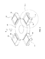
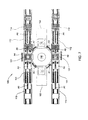
一実施形態においては、図1〜3に図示されるように、回転アクチュエータアセンブリ130は4つの印刷ネスト131を含み、これらは、各スクリーン印刷ヘッド102内で実行されるスクリーン印刷処理中に基板150を支持するようにそれぞれ構成される。図3は回転アクチュエータアセンブリ130の一実施形態の等角図であり、基板150が4つの印刷ネスト131のそれぞれの上に配置されている構成を示している。回転アクチュエータアセンブリ130は、回転アクチュエータ(図示せず)及びシステムコントローラ101の使用により軸Bを中心として回転し且つ角度をなして位置決めすることができ、印刷ネスト131をシステム内に望ましく位置決めすることができる。回転アクチュエータアセンブリ130は、印刷ネスト131の制御を促進する1つ以上のサポート構成要素又はシステム100において基板処理シーケンスを実行するために使用されるその他の自動制御装置も有していてよい。
In one embodiment, as illustrated in FIGS. 1-3, the
図4に図示されるように、各印刷ネスト131は一般に、送り出しスプール135及び巻き取りスプール136を有するコンベヤ139を備え、送り出しスプール及び巻き取りスプールは、生地137を送り出し、プラテン138上で生地を保持するように構成される。一実施形態において、生地137は多孔性材料であり、生地137の一方の面上に配置された基板150を、プラテン138に形成された真空ポートを利用して生地137の反対側に加えた真空によって、プラテン138に保持することができる。プラテン138は一般に基板支持表面を有し、スクリーン印刷ヘッド102において実行されるスクリーン印刷処理中、この基板支持表面上で、基板150及び生地137は支持され、また保持される。一実施形態において、生地137は薄い紙材である。一構成においては、ネスト駆動機構(図示せず)が送り出しスプール135及び巻き取りスプール136に連結されている又はこれらと係合するように構成されており、生地137上に位置決めされた基板150の移動を、印刷ネスト131内で正確に制御することができる。
As shown in FIG. 4, each
進入コンベヤ111及び退出コンベヤ112は一般に、基板150を支持し且つシステムコントローラ101と通信しているアクチュエータ(図示せず)の使用により基板をシステム100内の所望の位置に搬送可能である少なくとも1本のベルト116を含む。図1〜2では概して2本のベルト116を使用するスタイルの基板搬送システムを図示しているが、本発明の基本概念を変更することなく、その他のタイプの搬送機構を使用して同じ基板搬送・位置決め機能を実行することもできる。
The
一実施形態においては、図1〜2に示されるように、回転アクチュエータアセンブリ130が回転すると、印刷ネスト131は、進入コンベヤ111及び退出コンベヤ112の一部と交差する空間をすり抜ける。このような実施形態においては、回転アクチュエータアセンブリ130が自由に回転できるように、印刷ネスト131と進入、退出コンベヤ111、112との間での垂直軸(図1のB軸)に沿った相対運動が必要とされる。一実施形態において、進入及び退出コンベヤ111、112は印刷ネスト131の上方に位置決めすることができ、回転アクチュエータアセンブリ130の回転時、印刷ネスト131は進入及び退出コンベヤ111、112の下を通過する。別の実施形態においては、回転アクチュエータアセンブリ130全体及び全印刷ネスト131を、進入及び退出コンベヤ111、112との干渉を避けるために、垂直方向、即ち軸Bに対して平行に移動することができる。別の実施形態においては、個々の印刷ネストを、同じく進入及び退出コンベヤ111、112との干渉を避けるために垂直に移動させる。進入及び退出コンベヤ111、112、印刷ネスト131又は回転アクチュエータアセンブリ130の移動は、システムコントローラ101と通信している1つ以上の慣用のアクチュエータ装置の使用によって制御することができる。一実施形態において、印刷ネスト131は、リニアモータ(図示せず)及び印刷ネスト131を回転アクチュエータアセンブリ130に対する垂直方向に高い精度で位置決めするように構成されたその他のサポート構成要素に連結される。この構成において、リニアモータ及びその他のサポート構成要素は、印刷ネスト131を垂直方向に再現可能且つ正確に位置決めしてスクリーン印刷処理の結果を基板毎に目に見えて変化させないために使用される。
In one embodiment, as shown in FIGS. 1-2, as the
図6AA〜6HHに図示の別の実施形態において、進入及び退出コンベヤ111、112は、経路A(図1)の面における進入及び退出コンベヤ111、112の上方部の平行移動的な延長及び後退を通じて回転アクチュエータアセンブリ130が自由に回転できるように構成される。この実施形態において、進入及び退出コンベヤ111、112の上方及び下方部は、図6AA〜6HHに関連して以下で説明するように、経路Aに対して平行な、対向する並行移動的な延長及び後退が得られるように構成される。進入及び退出コンベヤ111、112の延長及び後退は、システムコントローラ101と通信しているアクチュエータ装置を通して制御することができる。アクチュエータ装置の例を図9A〜9Bに図示し、以下にて説明する。
In another embodiment, illustrated in FIGS. 6AA-6HH, the ingress and
一実施形態において、システム100は検査アセンブリ200も含み、この検査アセンブリは、スクリーン印刷処理の実行前及び実行後に基板150を検査するように構成される。この検査アセンブリ200は1つ以上のカメラ120を含む場合があり、これらのカメラは、図1、2に図示されるように、位置1、3に位置決めされた進入してくる又は処理済みの基板を検査するように位置決めされる。検査アセンブリ200は一般に少なくとも1つのカメラ120(例えば、CCDカメラ)及び検査を行い、その検査結果をシステムコントローラ101に送信可能なその他の電子部品を含むため、損傷した又は誤処理された基板を製造ラインから除去することができる。一実施形態において、各印刷ネスト131は、プラテン138上に位置決めされた基板150に光を照射するためのランプ又は同様のその他の光学的放射装置を備えており、検査アセンブリ200による検査がより容易となる。
In one embodiment, the
システムコントローラ101は一般にシステム100全体の制御及び自動制御を促進するように設計されており、典型的には中央処理装置(CPU)(図示せず)、メモリ(図示せず)及びサポート回路(又はI/O)(図示せず)を含むことができる。CPUは、様々なチャンバ処理及びハードウェア(例えば、コンベヤ、検出装置、モニタ、流体送出ハードウェア等)を制御するために工業環境で使用され且つシステム及びチャンバ処理を監視する(例えば、基板位置、処理時間、検出装置信号等)いずれの形態のコンピュータプロセッサの1つであってもよい。メモリはCPUに接続され、またランダムアクセスメモリ(RAM)、読み出し専用メモリ(ROM)、フロッピーディスク、ハードディスク、その他いずれの形式のローカル又はリモートデジタルストレージ等の容易に入手可能なメモリの1種以上であってもよい。CPUへの命令用にソフトウェア命令及びデータをコード化してメモリに保存することができる。サポート回路もまた、慣用のやり方でプロセッサをサポートするためにCPUに接続される。サポート回路には、キャッシュ、電源、クロック回路、入力/出力回路、サブシステム等を含めることができる。システムコントローラ101可読性のプログラム(又はコンピュータ命令)が、どのタスクを基板に実行可能かを決定する。好ましくは、このプログラムはシステムコントローラ101可読性のソフトウェアであり、少なくとも基板位置情報、コントロール対象である様々な構成要素の移動順序、基板検査システム情報及びこれらの組み合わせを生成し記憶するためのコードを含む。
The
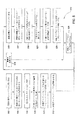
(搬送シーケンス)
図6A〜6H及び6AA〜6HHは、スクリーン印刷ヘッド102を使用して基板150の表面にパターン構造を形成するために使用される基板処理シーケンス500(図5)における異なる段階中のシステム100の代替実施形態の等角図である。図5、7に示される処理シーケンスは図6A〜6H及び6AA〜6HHに図示の段階に対応し、以下で説明される。図7は、図5の処理シーケンス500に従ってシステム100内を搬送される際に基板150がたどる搬送工程の例を示す。工程502〜512は、システム100にローディングされ、また処理される第1対の基板150についての初期処理シーケンス工程を示す。工程514〜526は、システム100へのローディング及びシステム100の稼動後に一般に行われる工程を示す。図6A〜6AAは、少なくとも一対の基板150が各搬入コンベヤ113上に位置決めされ、また進入コンベヤ111上へのローディング準備が整っている初期開始時点でのシステム100の構成の代替実施形態を図示している。
(Transport sequence)
6A-6H and 6AA-6HH are alternatives to the
図6Aに図示の実施形態において、進入コンベヤ111は、その上面が、基板150を搬送するために、対応する搬入コンベヤ113の上面と実質的に同一面上となるような上方位置にある状態で描かれている。図6AAに図示の実施形態において、進入コンベヤ111及び退出コンベヤ112の上方部210は後退位置にある状態で描かれている。この構成において、進入コンベヤ111は、搬入コンベヤ113から基板150を受け取るように構成され、また整列させられ、退出コンベヤ112は、基板を搬出コンベヤ114に搬送するように構成され、また整列させられる。
In the embodiment illustrated in FIG. 6A, the
図5、7に示される工程502において、各進入コンベヤ111は、搬送経路A1(図7)に沿って、それぞれの搬入コンベヤ113から第1対の基板150を受け取る。この構成においては、システムコントローラ101を使用して、各搬入コンベヤ113及び進入コンベヤ111に見られるベルト116及び駆動アクチュエータ(図示せず)の動きを連係させており、基板をこれらの自動制御構成要素間で信頼性高く搬送することができる。
In
図5、6B及び6BBに示される工程504において、第1対の基板150を次の処理シーケンス工程における位置1、3(図7)にある印刷ネスト131に送り出せるように各進入コンベヤ111を位置決めする。図6Bに図示の一実施形態においては、進入コンベヤ111を下降させて各印刷ネスト131と整列させる。進入コンベヤ111における基板支持面を下降させるためには、システムコントローラ101を使用して、進入コンベヤ111アセンブリ内に収められたアクチュエータ(図示せず)を制御する。図6BBに図示の代替実施形態においては、進入コンベヤ111及び退出コンベヤ112の上方部210を、各印刷ネスト131と実質的に整列した水平方向に延長する。進入コンベヤ111及び退出コンベヤ112の上方部210を平行移動的に延長するための機構の一実施形態については、図9A〜9Bに関連して以下で説明する。
In
図6C、6CC及び7に図示の工程506において、第1対の基板150は、進入コンベヤ111の各ベルト116から印刷ネスト131の生地137へと、搬送経路A2(図7)に沿って搬送される。この構成においては、システムコントローラ101を使用してベルト116及びネスト駆動機構(図示せず)の動きを連係させ、ネスト駆動機構を使用して、基板が印刷ネスト131内に信頼性高く位置決めされるように生地137を位置決めする。
In
工程508において、第1対の基板150を検査アセンブリ200内の構成要素によって検査し、印刷ネスト131上に破損した、欠けた又は亀裂が入った基板がないようにすることができる。この検査アセンブリは、各印刷ネスト131上での基板の正確な位置を測定する際にも使用することができる。システムコントローラ101は、各基板150の各印刷ネスト131上での位置データを使用してスクリーン印刷ヘッド102のスクリーン印刷ヘッド構成要素の位置決め及び方向づけを行い、続くスクリーン印刷処理の精度を向上させることができる。このケースにおいては、工程508で実行した検査過程中に受け取ったデータに基づいて、各スクリーン印刷ヘッド102の位置を自動的に調節し、印刷ネスト131上に位置決めされた基板の正確な位置に合わせることができる。
In
図5、6D及び6DDに示される工程510において、次の処理シーケンス工程中に実行される回転アクチュエータアセンブリ130の移動を妨害しないように、進入コンベヤ111及び退出コンベヤ112のそれぞれを位置決めする。図6Dに図示の実施形態において、進入コンベヤ111及び退出コンベヤ112は、進入コンベヤ111アセンブリ及び退出コンベヤ112アセンブリ内に収められたアクチュエータ(図示せず)及びシステムコントローラ101から送られた命令の使用によって上昇させられる。図6DDに図示の代替実施形態においては、各進入コンベヤ111の上方部210を水平方向に後退させる。これに対応して、各退出コンベヤ112の上方部210も同様に水平方向に後退させられる。進入及び退出コンベヤ111、112がこれらの後退位置にあると、回転アクチュエータアセンブリ130を、図6D、6DDに図示されるように自由に回転させることができる。
In
図5、6D、6DDに図示の工程512において、回転アクチュエータアセンブリ130を回転させると、第1対の基板のそれぞれが、搬送経路A3(図7)に沿ってスクリーン印刷ヘッド102内に位置決めされる。一実施形態においては、図6D、6DD及び7に図示されるように、回転アクチュエータアセンブリ130を90度回転させると、基板がスクリーン印刷ヘッド102内に位置決めされる。
In
工程514において、スクリーン印刷処理を実行して所望の材料を第1対の基板150の少なくとも一方の面上に堆積する。典型的には、スクリーン印刷処理は、完了までに約2秒かかる。一実施形態においては、基板スループットを向上させるために、工程514の実行中、工程515〜523を一般に並行して実行する。図5に示す偶数番号の工程が第1対の基板への実行を、奇数番号の工程が第2対の基板及び/又は代替対の基板への実行を意図されていることがわかる。
In
図5に示す工程515及び517において、進入コンベヤ111は第2対の基板150を各搬入コンベヤ113から受け取り、進入コンベヤ111は、図6A〜6B又は図6AA〜6BBに関連して上述した工程502、504の手順と同様にして、第2対の基板150を印刷ネスト131に送り出せるように位置決めされる。一連の工程515〜525のうちの一部の工程を、処理シーケンス500中に実行されるその他の工程の1つ以上と同時に実行してもよいことに留意すべきである。例えば、工程515を工程512の実行中に実行することができ、或いは工程519を工程515、517の実行中に実行することができる。
In
定常状態の基板処理中(全ての印刷ネストに基板がローディング済みである等)、上述した工程512中に回転アクチュエータアセンブリ130を駆動するに先立って、一対の基板150がスクリーン印刷ヘッド102内で既に処理されてしまっていることがわかる。従って、工程519において、回転アクチュエータ位置1、3(図6E、6EE、7)に位置決めされた既に処理済みの基板を今度は検査アセンブリ200で検査して、破損した、欠けた又は亀裂の入った基板が無く、印刷処理の質がユーザ定義基準に沿うかを確認することができる。
During steady state substrate processing (e.g., all of the printing nests have been loaded with a substrate), prior to driving the
図5、6E、6EE及び7に示される工程521において、第2対の基板150を、今度は進入コンベヤ111の各ベルト116から印刷ネスト131の生地137へと、搬送経路A2(図7)に沿って搬送することができ、上述の工程506と同様である。
In
しかしながら、システム100内での定常状態の処理中、一対の基板150は、工程512における回転アクチュエータアセンブリ130の駆動に先立って既にスクリーン印刷ヘッド102内で処理されてしまっているため、第2対の基板150を印刷ネスト131上にローディングする前に処理済みの基板150を印刷ネスト131から除去する必要がある。一実施形態においては、既に処理済みの対の基板150を印刷ネスト131から移動させ(即ち、図7の搬送経路A4)、第2対の基板を印刷ネスト131へと一般に同時に搬送する(即ち、図7の搬送経路A2)。処理済みの基板を印刷ネスト131から除去したら、退出コンベヤ112に送り出された処理済みの基板150を次に各搬出コンベヤ114へと、搬送経路A5(図7)に沿って送り出すことができる。図6Fに図示の一実施形態においては、処理済みの基板150を受け取った後、各退出コンベヤ112を上昇させて、各搬出コンベヤ114と垂直方向で整列させる。図6FFに図示の代替実施形態において、各退出コンベヤ112は、既に処理済みの基板150を搬出コンベヤ114へと送り出す構成に既になっている。システムコントローラ101を使用して各退出コンベヤ112及び搬出コンベヤ114に見られるベルト116及び駆動アクチュエータ(図示せず)の動きを連係させており、基板をこれらの自動制御構成要素間で信頼性高く搬送することができる。次に、搬出コンベヤ114は、処理済みのこの基板150を製造ラインのその他の部品へと搬送経路A6に沿って搬送することができる。
However, during steady state processing in the
図6G及び6GGは、退出コンベヤ112上に移動させられた後の既に処理済みの対の基板150及び印刷ネスト131上に搬送された後の第2対の基板150の位置を示す。この構成においては、システムコントローラ101を使用して進入コンベヤ111のベルト116の動き、生地137の移動及び退出コンベヤ112のベルト116の動きを連係させており、基板を信頼性高く搬送することができる。
FIGS. 6G and 6GG show the position of the already processed pair of
工程523において、第2対の基板150を、検査アセンブリ200の構成要素によって任意で検査して、印刷ネスト131上に破損した、欠けた又は亀裂が入った基板がないことを確認することができ、また各印刷ネスト131上の基板の正確な位置を、上述した工程508と同様に測定することができる。
In
図5、6H及び6HHに示される工程525において、進入コンベヤ111及び退出コンベヤ112のそれぞれは、次の処理シーケンス工程における回転アクチュエータアセンブリ130の移動を妨害しないように位置決めされる。図6Hに図示の実施形態において、進入コンベヤ111及び退出コンベヤ112は、進入コンベヤ111及び退出コンベヤ112に収められたアクチュエータ(図示せず)並びにシステムコントローラ101から送られた命令の使用によって上昇させられる。図6HHに図示の代替実施形態において、進入コンベヤ111の上方部210は印刷ネスト131から水平方向に後退させられ、また退出コンベヤ112の上方部210も同様に印刷ネスト131から後退させられる。一実施形態において、システムコントローラ101は、進入及び退出コンベヤ111、112の上方部210の後退を制御するための命令を送る。
In
図5、7に示される工程526で、回転アクチュエータアセンブリ130を回転させると、第2対の基板のそれぞれがスクリーン印刷ヘッド102内に搬送経路A3(図7)に沿って位置決めされ、第1対の基板が回転アクチュエータ位置1、3に搬送経路A7(図6E、6EE、7)に沿って位置決めされる。一実施形態において、図6D、6DD及び7に図示されるように、回転アクチュエータアセンブリ130は、工程526中、約90度回転させられる。
When the
工程526が完了したら、システム100において処理する予定の基板の枚数に応じて、工程514~526を何度も繰り返すことができる。図5に示した工程の数及び順序は本明細書に記載の発明の範囲を限定することを意図していないことに留意すべきである。これは、本明細書に記載の発明の基本的な範囲から逸脱することなく1つ以上の工程を省略及び/又は並べ替え可能であるためである。また、図5に示した概略工程図は、本明細書に記載の発明の範囲を限定することを意図していないが、これは、これらの工程を図で示したような連続的な形で完了する必要はなく、2つ以上の工程を同時に完了することも可能だからである。
When
検査アセンブリ200が破損した又は不具合のある基板を検出した場合、基板は廃棄物回収装置117(図1)に置かれてプロセス流れから排除されるため、残りの下流の処理に被害や影響を与えることがない。図8A、8Bを参照するが、印刷ネスト131のうちの1つの上に位置決めされた不具合のある基板150Aを、廃棄物回収装置117に移動させる必要がある。一実施形態においては、この不具合のある基板150Aを除去するために、退出コンベヤ112を上昇させ(図8B)、不具合のある基板を、システムコントローラ101から送られた命令をうけた印刷ネスト131における生地137の移動によって、印刷ネスト131から廃棄物回収装置117の1つに移動させる。代替実施形態においては、上方部210を後退させて、不具合のある基板を印刷ネスト131から廃棄物回収装置117に搬送することができる。
If the
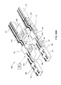
(進入及び退出コンベヤの構成)
図6AA~6HHに図示の実施形態において、進入及び退出コンベヤ111、112は、そのそれぞれの上方部210が水平方向に延びて基板150を印刷ネスト131から受け取り又は印刷ネスト131へと送り出し、また水平方向に後退することによって回転アクチュエータアセンブリ130の自由な回転を可能にするように構成される。図9A、9Bは、本発明の一実施形態による進入コンベヤ111の簡略化された概略断面図である。以下の説明では進入コンベヤ111に言及するが、この説明は、進入コンベヤと全く同じとなり得る退出コンベヤ112にも同様にあてはまる。
(Configuration of entry and exit conveyors)
In the embodiment illustrated in FIGS. 6AA-6HH, the entry and exit
図9A、9Bに図示されるような一実施形態において、進入コンベヤ111は、上方部210、下方部220及びその間に配置された固定ピニオンギア230を備える。固定ピニオンギア230は、進入コンベヤ111の上方及び下方部210、220を同時に水平方向に延長、後退させるためのピニオンギアモータ240によって駆動される。上方部210は、1本以上のベルト116をその上で支持するように構成された上面212を有する構造ラックであってもよい。上方部210の下部214には、固定ピニオンギア230のものとマッチするギア歯を形成することができる。これに対応して、下方部220は、固定ピニオンギア230のものとマッチするギア歯を備えた上部224及び1本以上のベルト116をその上で誘導するように構成された下面222を有する構造ラックであってもよい。
In one embodiment as illustrated in FIGS. 9A, 9B, the
一実施形態において、上方部210は、一端で固定された上方ローラ216を含む。上方ローラ217は反対側に構成されており、また上方部210を延長、後退させても静止したままとなるように構成される。各上方ローラ216、217は、自由に回転して上方部210の上面212上でベルト116を誘導するように構成することができる。これに対応して、下方部220も同じく一端で固定された下方ローラ226を含むことができる。下方部220も自由に回転して下方部220の下面222上へとベルト116を誘導するように構成することができる。
In one embodiment, the
一実施形態において、進入コンベヤ111は、基板150を輸送するために1本以上のベルト116を駆動し、また誘導するためのコンベヤベルトモータ260によって駆動される1つ以上のドライバローラ250を含む。一実施形態において、進入コンベヤ111は、1本以上のベルト116を誘導し、またベルトをピンと張るための1つ以上のアイドルローラ270を含む。加えて、進入コンベヤ111は、進入コンベヤ111の特定の構成及びサイズの必要に応じて1本以上のベルト116を誘導するための1つ以上の追加のフリーホイーリングローラ280を含む場合がある。
In one embodiment, the
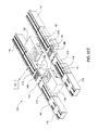
運転中、まず進入コンベヤ111を、図9Aに図示されるようなその後退位置に位置決めすることができる。上述したように、進入コンベヤ111がその後退位置にある場合(また退出コンベヤ112がその後退位置にある場合)、回転アクチュエータアセンブリ130は、印刷ネスト131をB軸(図6AA~6HH)を中心として自由に回転させることができる。基板150を、搬入コンベヤ113から進入コンベヤ111へと搬送することができる。この時点で、基板150を印刷ネスト131上に送り出すために、進入コンベヤ111を、図9Aに図示されるようなその後退位置から図9Bに図示されるようなその延長位置に延長することができる。
During operation, the
一実施形態において、以下の操作は、上方部210のその後退位置からその延長位置への延長を完了するために行われる。システムコントローラ101は、ピニオンギアモータ240に信号を送ることによって、ピニオンギア230をC方向に回転させる。ピニオンギア230が回転するにつれ、上方部210はX方向に水平に延長され、同時に下方部220はY方向に後退する。一実施形態において、システムコントローラ101は、1本以上のベルト116を駆動するために、実質的に同時に信号をコンベヤベルトモータ260に送って1つ以上のドライバローラ250をF方向に回転させる。実質的に同時のベルト116の駆動及び上方部210の平行移動によって、基板150を、受け取り位置(図9A)から送り出し位置(図9B)へと迅速に移動させることができる。進入コンベヤの上方部210をその延長位置からその後退位置に後退させるには、ドライバローラ250の回転方向以外、先行の操作を実質的に逆に行う。ドライバローラ250の回転方向は常に同じままである。
In one embodiment, the following operations are performed to complete the extension of the
上述したように、退出コンベヤ112の構成及び操作は、進入コンベヤ111のものと実質的に同じである。
As described above, the configuration and operation of the
(代替のコンベヤスクリーン印刷システム構成)
図10は、システム100の別の実施形態、即ちシステム100Aを図示しており、進入コンベヤ111及び退出コンベヤ112は、回転アクチュエータアセンブリ130が様々な位置1〜4の間で回転できるように進入コンベヤ111及び退出コンベヤ112を印刷ネスト131に対して移動させる必要がないような形状になっている。このため、この構成では搬送シーケンス時間を短縮し、また進入コンベヤ111及び退出コンベヤ112のコストを削減することができる。
(Alternative conveyor screen printing system configuration)
FIG. 10 illustrates another embodiment of the
図10を参照するが、システム100Aは一般に2つの進入コンベヤ111と、回転アクチュエータアセンブリ130と、2つのスクリーン印刷ヘッド102と、2つの退出コンベヤ112と、回転アクチュエータアセンブリ130に取り付けられ且つ回転アクチュエータアセンブリと共に回転する四対のサポートコンベヤ133を含む。システム100Aは一般に、並行処理構成に構成された2つの進入コンベヤ111を利用しており、各進入コンベヤ111は、進入コンベヤ111のベルト116及びサポートコンベヤ133のベルトを使用して搬入コンベヤ113から基板を受け取り、この基板を回転アクチュエータアセンブリ130に連結された印刷ネスト131に搬送することができる。また、各退出コンベヤ112は一般に、サポートコンベヤ133のベルト及び進入コンベヤ111のベルト116を使用して印刷ネスト131から処理済みの基板を受け取り、この処理済みの基板のそれぞれを搬出コンベヤ114に搬送するように構成される。
Referring to FIG. 10, the
システム100Aにおける基板の搬送に使用される処理シーケンス工程は、図5に示される工程と同様である。主な違いには、進入又は退出コンベヤ111、112の位置を変更してコンベヤを印刷ネスト131に整列させる又はコンベヤを移動させて回転アクチュエータアセンブリ130の移動を妨害しないようにする必要がないことである。このケースにおいて、システム100と共に使用される処理シーケンス500に見られる工程504、510、517、525は一般に必要とされない。処理シーケンスのその他の大きな違いには、システムコントローラ101が、ローディング工程中の進入コンベヤ111のベルト及び印刷ネスト131の生地137の移動(即ち、工程506、521)に伴うサポートコンベヤ133の移動並びにアンローディング工程(即ち、工程521)中のサポートコンベヤ133の移動、退出コンベヤ112のベルト及び印刷ネスト131の生地137の移動も制御するという追加要件も含まれる。一例において、システム100における基板搬送経路は一般に経路B1〜B7をたどる。
The processing sequence process used for transporting the substrate in the
(代替のスクリーン印刷システム構成)
図11は、本明細書に記載の発明の様々な実施形態と共に使用し得るマルチスクリーン印刷チャンバ処理システムの代替の構成、即ちシステム1000を示す。システム1000は上述のシステム100の構成と同様であるが、1つの進入コンベヤ111及び退出コンベヤ112を使用して基板を回転アクチュエータアセンブリ130及び1対のスクリーン印刷ヘッド102に送り出す。進入コンベヤ111及び退出コンベヤ112を1つ除去することによって、システム全体のコストを削減することができる。図11を理解しやすくするために、図1〜10で使用のものと同じ参照番号を、可能な場合は、図に共通する同一要素を表すのに使用している。図11に図示の構成において、印刷ネスト131は、ネスト上での基板の移動方向が、回転アクチュエータアセンブリ130に対して半径方向に方向づけられるように方向づけされる。
(Alternative screen printing system configuration)
FIG. 11 illustrates an alternative configuration of a multi-screen printing chamber processing system,
一実施形態において、システム1000は、1つの進入コンベヤ111と、回転アクチュエータアセンブリ130と、2つのスクリーン印刷ヘッド102と、中央コンベヤアセンブリ1010と、1つの退出コンベヤ112とを備える。システム1000は一般に1つの進入コンベヤ111を利用して基板を位置1(図11)に位置決めされた印刷ネスト131に送り出し、また退出コンベヤ112を利用して位置3に位置決めされた印刷ネスト131から基板を除去する。搬入コンベヤ113、進入コンベヤ111、印刷ネスト131、退出コンベヤ112及び搬出コンベヤ114間での基板の移動は、上述の動きと同様である。しかしながら、システム1000には上述の処理シーケンスより有利な点がある。様々な位置1〜4間で回転アクチュエータアセンブリ130が回転できるように進入コンベヤ111及び退出コンベヤ112を印刷ネスト131に対して移動させる必要がないからである。このため、この構成によって、搬送シーケンス時間を短縮し、また進入コンベヤ111及び退出コンベヤ112のコストを削減することができる。
In one embodiment, the
中央コンベヤアセンブリ1010は一般に、基板150を回転アクチュエータアセンブリ130を越えて反対側の印刷ネストに搬送可能なコンベヤ又は同様のロボット装置であるため、基板を反対側の印刷ネスト、退出コンベヤ及び/又は搬出コンベヤに搬送することができる。一実施形態において、中央コンベヤアセンブリ1010は、基板を、位置1に位置決めされた印刷ネストから位置3に位置決めされた印刷ネストへと、位置1及び3に位置決めされた印刷ネストの生地137の連係運動並びに中央コンベヤアセンブリ1010のベルト1011の移動によって搬送するように構成される。一実施形態において、中央コンベヤアセンブリ1010は、回転アクチュエータアセンブリ130と一緒に回転し且つこのため対向する印刷ネスト131のそれぞれの対ときっちりと整列する2組のローラ又はベルトを備える。別の実施形態において、中央コンベヤアセンブリ1010は静止したままであり、基板を、位置1に位置決めされた印刷ネストから位置3に位置決めされた印刷ネストにのみ搬送可能なように整列される。
Since the
図12は、システム1000における基板処理シーケンス1100の一例を示す。図12は、図12の処理シーケンスに従って基板がシステム1000内を搬送される際にたどる基板の搬送工程の例を示す。工程1102〜1112は、第1対の基板に関しての主な初期処理シーケンス工程を示し、工程1114〜1126は、システム1000のローディング及び運転中に一般に実行される工程を示す。
FIG. 12 shows an example of a
図11及び12に示される工程1102において、進入コンベヤ111は、第1対の基板150を搬送経路C1(図11)に沿って搬入コンベヤ113から受け取る。この構成においては、システムコントローラ101を使用して搬入コンベヤ113及び進入コンベヤ111に見られるベルト116及び駆動アクチュエータ(図示せず)の動きを連係させており、基板をこれらの自動制御構成要素間で信頼性高く搬送することができる。
In
図11及び12に示される工程1106において、第1対の基板150は、進入コンベヤ111のベルト116から印刷ネスト131の生地137へと搬送経路C2及びC4(図11)に沿って搬送される。この構成においては、システムコントローラ101を使用して進入コンベヤ111のベルト116、位置1に位置決めされた印刷ネスト131の材料137、中央コンベヤアセンブリ1010のベルト1011、位置3に位置決めされた印刷ネスト131の生地137、中央コンベヤアセンブリ101のベルト1011及び位置3に位置決めされた印刷ネスト131の生地137の動きを連係させており、1枚の基板を位置1、3に位置決めされた印刷ネストのそれぞれに位置決めすることができる。一実施形態において、進入コンベヤ111から受け取った基板は所望の間隔(即ち、位置1、3に位置決めされた印刷ネスト131間の距離)で離間されるため、全ての自動制御構成要素の速度を一定に維持することができ、基板を、ほぼ同じ時間にそのそれぞれの印刷ネストに簡単に位置決めすることができる。
11 and 12, the first pair of
工程1108において、第1対の基板150を、検査アセンブリ200の構成要素によって任意で検査して、印刷ネスト131上に破損した、欠けた又は亀裂が入った基板がないことを確認してもよい。この検査アセンブリは、各印刷ネスト131上の基板の正確な位置を測定するために使用することもできる。システムコントローラ101は、各基板150の各印刷ネスト131上での位置データを利用してスクリーン印刷ヘッド102におけるスクリーン印刷ヘッド構成要素の位置決め及び方向づけを行うことができるため、続くスクリーン印刷処理を、各基板150上で正確に位置決めすることができる。このケースにおいては、工程1108で実行した検査過程中に受け取ったデータに基づいて、各印刷ヘッドの位置を自動的に調節し、印刷ネスト上に位置決めされた基板の正確な位置にスクリーン印刷ヘッド102を整列させることができる。
In
図11及び図12に示される工程1112において、回転アクチュエータアセンブリ130を回転させると、第1対の基板のそれぞれが、搬送経路A3(図10)に沿ってスクリーン印刷ヘッド102内に位置決めされる。一実施形態においては、図10に図示されるように、回転アクチュエータアセンブリ130を90度回転させると、基板がスクリーン印刷ヘッド102内に位置決めされる。
In
工程1114において、スクリーン印刷処理を実行して所望の材料を第1対の基板150の少なくとも一方の面上に堆積する。一実施形態においては、基板スループットを向上させるために、工程1114の実行中、工程1115〜1123を一般に並行して実行する。奇数番号の工程が第1対の基板への実行を、偶数番号の工程を第2対の基板及び/又は代替対の基板への実行を意図されていることがわかる。
In
図12に示される工程1115において、進入コンベヤ111は第2対の基板150を搬入コンベヤ113から受け取り、進入コンベヤ111は、上述の工程1102の手順と同様にして、この第2対の基板150を印刷ネスト131に送り出せるように位置決めされる。一連の工程1115〜1125のうちの一部の工程を、処理シーケンス1100中に実行される1つ以上の工程と同時に実行してもよいことに留意すべきである。例えば、工程1115を工程1112の実行中に実行することができ、或いは工程1112を工程1115の実行中に実行することができる。
In
システム1000における定常状態の基板処理中(全ての印刷ネストに基板がローディング済みである等)、上述の工程1112中に回転アクチュエータアセンブリ130を駆動するに先立って、一対の基板がスクリーン印刷ヘッド102内で既に処理されてしまっていることがわかる。従って、工程1119において、回転アクチュエータ位置1、3(図11)の印刷ネスト131に位置決めされた既に処理済みの基板を今度は検査アセンブリ200の構成要素で検査して、破損した、欠けた又は亀裂の入った基板が無いことを確認し、また印刷処理の質を監視することができる。
During steady state substrate processing in the system 1000 (such as substrates loaded in all print nests), a pair of substrates are placed in the
図11及び12に示される工程1121において、ここで第2対の基板150を、進入コンベヤ111の各ベルト116から印刷ネスト131の生地137へと、搬送経路C2、C4(図7)に沿って搬送することができ、工程506で同様に上述したとおりである。この構成においては、システムコントローラ101を使用して進入コンベヤ111のベルト116、位置1に位置決めされた印刷ネスト131の材料137、中央コンベヤアセンブリ1010のベルト1011及び位置3に位置決めされた印刷ネスト131の生地137の動きを連係させており、1愛の基板を位置1、3に位置決めされた印刷ネストのそれぞれに位置決めすることができ、工程1106に関連して上述した通りである。一実施形態において、進入コンベヤ111から受け取った基板は所望の間隔(即ち、位置1、3に位置決めされた印刷ネスト131間の距離)で離間されるため、全ての自動制御構成要素の速度を一定に維持することができ、基板を、ほぼ同じ時間にそのそれぞれの印刷ネストに簡単に位置決めすることができる。
11 and 12, a second pair of
しかしながら、システム100内での定常状態の処理中、一対の基板は、工程1112における回転アクチュエータアセンブリ130の駆動に先立って既にスクリーン印刷ヘッド102内で処理されてしまっているため、第2対の基板を印刷ネスト131上にローディングする前に処理済みの基板を印刷ネスト131から除去する必要がある。一実施形態においては、既に処理済みの基板対を印刷ネスト131から移動させ(即ち、図10の搬送経路C4、C5)、第2対の基板を印刷ネスト131へと一般に同時に搬送する(即ち、搬送経路C2、C4)。このケースにおいては、位置1に位置決めされた処理済みの基板を、システムコントローラ101から送られた命令をうけた上での位置1に位置決めされた印刷ネスト131の生地137、中央コンベヤアセンブリ1010のベルト1011及び位置3に位置決めされた印刷ネスト131の生地137の動き並びに退出コンベヤ112のベルト116の動きによって、退出コンベヤ112に移動させる必要がある。位置3に位置決めされた処理済みの基板は、位置1にある基板が移動させられたら、システムコントローラ101からの命令をうけた上での位置3に位置決めされた印刷ネスト131の生地137の動き及び退出コンベヤ111のベルト116の動きにより退出コンベヤ112へと同時に移動することが可能である。一実施形態において、既に処理済みの基板の回転アクチュエータアセンブリ130からの移動及び新しく搬入された基板の回転アクチュエータアセンブリ130への移動は、連続的に同時に行われる。
However, during steady state processing in the
印刷ネスト131から退出コンベヤ112に送られた処理済みの基板を次に搬出コンベヤ114のそれぞれに搬送経路C5(図11)に送り出すことができる。この構成においては、システムコントローラ101を使用して退出コンベヤ112及び搬出コンベヤ114に見られるベルト116及び駆動アクチュエータ(図示せず)の動きを連係させており、基板をこれらの自動制御構成要素間で信頼性高く搬送することができる。次に、搬出コンベヤ114は、処理済みの基板を製造ラインのその他の部品へと搬送経路C6に沿って搬送することができる。
The processed substrate sent from the
工程1123において、第2対の基板150を、検査アセンブリ200の構成部品によって任意で検査して、印刷ネスト131上に破損した、欠けた又は亀裂が入った基板がないことを確認し、また各印刷ネスト131上の基板の正確な位置を、上述した工程508、1108と同様に測定することができる。
In
図11、12に示される工程1126で、回転アクチュエータアセンブリ130を回転させると、第2対の基板のそれぞれがスクリーン印刷ヘッド102内に搬送経路C3(図11)に沿って位置決めされ、第1対の基板が回転アクチュエータ位置1、3に搬送経路C7(図11)に沿って位置決めされる。一実施形態においては、図11に図示されるように、回転アクチュエータアセンブリ130を約90度回転させると、基板がスクリーン印刷ヘッド102内に位置決めされる。
In
工程1126が完了したら、システム1000において処理する予定の基板の枚数に応じて、工程1114~1126を何度も繰り返すことができる。図12に示した工程の数及び順序は本明細書に記載の発明の範囲を限定することを意図していないことに留意すべきである。これは、本明細書に記載の発明の基本的な範囲から逸脱することなく1つ以上の工程を省略及び/又は並べ替え可能であるためである。また、図12に示した概略工程図は、本明細書に記載の発明の範囲を限定することを意図していないが、これは、上述したようにこれらの工程を図で示したような連続的な形で完了する必要はなく、1つ以上の工程を同時に完了することもできるからである。
When
上記は本発明の実施形態を対象としているが、本発明の基本的な範囲から逸脱することなく本発明のその他及び更に別の実施形態を創作することができ、本発明の範囲は、以下の特許請求の範囲に基づいて定められる。 While the above is directed to embodiments of the present invention, other and further embodiments of the invention may be made without departing from the basic scope of the invention. It is determined based on the scope of claims.
Claims (15)
回転軸を有する回転アクチュエータと、
回転アクチュエータにそれぞれ連結された第1基板支持体及び第2基板支持体と、
回転アクチュエータが第1方向に角度をなして位置決めされた場合に基板を第1基板支持体に搬送するように位置決めされた第1コンベヤと、
回転アクチュエータが第1方向に角度をなして位置決めされた場合に基板を第1基板支持体から受け取るように位置決めされた第2コンベヤと、
回転アクチュエータが第1方向に角度をなして位置決めされた場合に基板を第2基板支持体に搬送するように位置決めされた第3コンベヤと、
回転アクチュエータが第1方向に角度をなして位置決めされた場合に基板を第2基板支持体から受け取るように位置決めされた第4コンベヤとを備える装置。 An apparatus for depositing pattern material on a substrate surface,
A rotary actuator having a rotation axis;
A first substrate support and a second substrate support respectively coupled to the rotary actuator;
A first conveyor positioned to convey a substrate to a first substrate support when the rotary actuator is positioned at an angle in a first direction;
A second conveyor positioned to receive a substrate from the first substrate support when the rotary actuator is positioned at an angle in the first direction;
A third conveyor positioned to convey the substrate to the second substrate support when the rotary actuator is positioned at an angle in the first direction;
A fourth conveyor positioned to receive the substrate from the second substrate support when the rotary actuator is positioned at an angle in the first direction.
回転アクチュエータが第1方向に角度をなして位置決めされた場合に第3基板支持体を受け取るように位置決めされた第1スクリーン印刷チャンバと、
回転アクチュエータが第1方向に角度をなして位置決めされた場合に第4基板支持体を受け取るように位置決めされた第2スクリーン印刷チャンバと、
回転アクチュエータが第1方向に角度をなして位置決めされた場合に第1基板支持体上に配置された基板を監視するように位置決めされた第1カメラと、
回転アクチュエータが第1方向に角度をなして位置決めされた場合に第2基板支持体上に配置された基板を監視するように位置決めされた第2カメラとを更に備える、請求項1記載の装置。 A third substrate support and a fourth substrate support respectively connected to the rotary actuator;
A first screen printing chamber positioned to receive a third substrate support when the rotary actuator is positioned at an angle in a first direction;
A second screen printing chamber positioned to receive a fourth substrate support when the rotary actuator is positioned at an angle in the first direction;
A first camera positioned to monitor a substrate disposed on the first substrate support when the rotary actuator is positioned at an angle in a first direction;
The apparatus of claim 1, further comprising a second camera positioned to monitor a substrate disposed on the second substrate support when the rotary actuator is positioned at an angle in the first direction.
第2コンベヤの少なくとも一部を、第1回転軸に実質的に平行である第2方向に沿って第1位置から第2位置へと移動するように構成されたアクチュエータとを更に備える、請求項3記載の装置。 An actuator configured to move at least a portion of the first conveyor from a first position to a second position along a first direction substantially parallel to the first axis of rotation;
The actuator further comprising at least a portion of the second conveyor configured to move from the first position to the second position along a second direction substantially parallel to the first axis of rotation. 3. The apparatus according to 3.
回転軸を有する回転アクチュエータと、
回転アクチュエータにそれぞれ連結された第1基板支持体及び第2基板支持体と、
ベルト部材を支持するための上方部を備えた第1コンベヤを備え、第1コンベヤの上方部は、後退位置と延長位置との間を移動するように構成されており、また第1コンベヤの上方部は、回転アクチュエータが第1方向に角度をなして位置決めされた場合、また第1コンベヤの上方部が延長位置に位置決めされた場合に、基板を第1基板支持体に搬送するように位置決めされ、
装置が更に、
ベルト部材を支持するための上方部を備えた第2コンベヤを備え、第2コンベヤの上方部は、後退位置と延長位置との間を移動するように構成されており、また第2コンベヤの上方部は、回転アクチュエータが第1方向に角度をなして位置決めされ、また第2コンベヤの上方部が延長位置に位置決めされた場合に、基板を第2基板支持体に搬送するように位置決めされる装置。 An apparatus for depositing pattern material on a substrate surface,
A rotary actuator having a rotation axis;
A first substrate support and a second substrate support respectively coupled to the rotary actuator;
A first conveyor having an upper portion for supporting a belt member, wherein the upper portion of the first conveyor is configured to move between a retracted position and an extended position; The portion is positioned to transport the substrate to the first substrate support when the rotary actuator is positioned at an angle in the first direction and when the upper portion of the first conveyor is positioned at the extended position. ,
The device further
A second conveyor having an upper portion for supporting a belt member, the upper portion of the second conveyor being configured to move between a retracted position and an extended position; and above the second conveyor The device is positioned to convey the substrate to the second substrate support when the rotary actuator is positioned at an angle in the first direction and the upper portion of the second conveyor is positioned in the extended position. .
ベルト部材を支持するための上方部を備えた第4コンベヤを更に備え、
第4コンベヤの上方部は、延長位置と後退位置との間を移動するように構成されており、また第4コンベヤの上方部は、回転アクチュエータが第1方向に角度をなして位置決めされ、また第4コンベヤの上方部が延長位置に位置決めされた場合に、基板を第2基板支持体から受け取るように位置決めされる、請求項6記載の装置。 A third conveyor having an upper portion for supporting the belt member, the upper portion of the third conveyor being configured to move between an extended position and a retracted position; The upper portion is positioned to receive the substrate from the first substrate support when the rotary actuator is positioned at an angle in the first direction and when the upper portion of the third conveyor is positioned in the extended position. ,
A fourth conveyor having an upper portion for supporting the belt member;
The upper part of the fourth conveyor is configured to move between an extended position and a retracted position, and the upper part of the fourth conveyor is positioned at an angle in the first direction by the rotary actuator, and The apparatus of claim 6, wherein the substrate is positioned to receive the substrate from the second substrate support when the upper portion of the fourth conveyor is positioned in the extended position.
回転アクチュエータが第1方向に角度をなして位置決めされた場合に第3基板支持体を受け取るように位置決めされた第1スクリーン印刷チャンバと、
回転アクチュエータが第1方向に角度をなして位置決めされた場合に第4基板支持体を受け取るように位置決めされた第2スクリーン印刷チャンバと、
回転アクチュエータが第1方向に角度をなして位置決めされた場合に第1基板支持体上に配置された基板を監視するように位置決めされた第1カメラと、
回転アクチュエータが第1方向に角度をなして位置決めされた場合に第2基板支持体上に配置された基板を監視するように位置決めされた第2カメラとを更に備える、請求項6記載の装置。 A third substrate support and a fourth substrate support respectively connected to the rotary actuator;
A first screen printing chamber positioned to receive a third substrate support when the rotary actuator is positioned at an angle in a first direction;
A second screen printing chamber positioned to receive a fourth substrate support when the rotary actuator is positioned at an angle in the first direction;
A first camera positioned to monitor a substrate disposed on the first substrate support when the rotary actuator is positioned at an angle in a first direction;
The apparatus of claim 6, further comprising a second camera positioned to monitor a substrate disposed on the second substrate support when the rotary actuator is positioned at an angle in the first direction.
回転軸を有する回転アクチュエータと、
回転アクチュエータにそれぞれ連結された第1基板支持体及び第2基板支持体を備え、第1基板支持体及び第2基板支持体は、回転アクチュエータの両側に位置決めされ、
装置が更に、
第1基板支持体と第2基板支持体との間で基板を搬送するように位置決めされた第1コンベヤと、
回転アクチュエータが第1方向に角度をなして位置決めされた場合に基板を第1基板支持体に搬送するように位置決めされた第2コンベヤと、
回転アクチュエータが第1方向に角度をなして位置決めされた場合に基板を第2基板支持体から受け取るように位置決めされた第3コンベヤとを備える装置。 An apparatus for depositing pattern material on a substrate surface,
A rotary actuator having a rotation axis;
A first substrate support and a second substrate support respectively connected to the rotary actuator, wherein the first substrate support and the second substrate support are positioned on both sides of the rotary actuator;
The device further
A first conveyor positioned to transport a substrate between the first substrate support and the second substrate support;
A second conveyor positioned to transport the substrate to the first substrate support when the rotary actuator is positioned at an angle in the first direction;
A third conveyor positioned to receive the substrate from the second substrate support when the rotary actuator is positioned at an angle in the first direction.
回転アクチュエータが第1方向に角度をなして位置決めされた場合に第3基板支持体を受け取るように位置決めされた第1スクリーン印刷チャンバと、
回転アクチュエータが第1方向に角度をなして位置決めされた場合に第4基板支持体を受け取るように位置決めされた第2スクリーン印刷チャンバと、
回転アクチュエータが第1方向に角度をなして位置決めされた場合に第1基板支持体上に配置された基板を監視するように位置決めされた第1カメラと、
回転アクチュエータが第1方向に角度をなして位置決めされた場合に第2基板支持体上に配置された基板を監視するように位置決めされた第2カメラとを更に備える、請求項10記載の装置。 A third substrate support and a fourth substrate support respectively connected to the rotary actuator and positioned on both sides thereof;
A first screen printing chamber positioned to receive a third substrate support when the rotary actuator is positioned at an angle in a first direction;
A second screen printing chamber positioned to receive a fourth substrate support when the rotary actuator is positioned at an angle in the first direction;
A first camera positioned to monitor a substrate disposed on the first substrate support when the rotary actuator is positioned at an angle in a first direction;
11. The apparatus of claim 10, further comprising a second camera positioned to monitor a substrate disposed on the second substrate support when the rotary actuator is positioned at an angle in the first direction.
第1コンベヤ上で第1基板を、第2コンベヤ上で第2基板を受け取り、
回転アクチュエータが第1角度位置に方向づけされている間に第1基板を第1基板支持体に搬送し、
回転アクチュエータが第1角度位置に方向づけされている間に第2基板を第2基板支持体に搬送し、ここで第1基板の第1基板支持体への搬送及び第2基板の第2基板支持体への搬送は一般に同時に行われ、
第3基板支持体が基板を第1コンベヤから受け取るように位置決めされ、また第4基板支持体が基板を第2コンベヤから受け取るように位置決めされるように回転アクチュエータを第1角度位置から第2角度位置へと回転させ、
回転アクチュエータが第2角度位置に方向づけされた場合に、第1スクリーン印刷チャンバ内の第1基板支持体上に配置された第1基板上に材料を堆積し、
回転アクチュエータが第2角度位置に方向づけされた場合に、第2スクリーン印刷チャンバ内の第2基板支持体上に配置された第2基板上に材料を堆積することを含む、基板を処理するための方法。 Directing a rotary actuator having a first substrate support, a second substrate support, a third substrate support and a fourth substrate support to a first angular position;
Receiving a first substrate on a first conveyor and a second substrate on a second conveyor;
Transporting the first substrate to the first substrate support while the rotary actuator is oriented to the first angular position;
While the rotary actuator is oriented to the first angular position, the second substrate is transferred to the second substrate support, where the first substrate is transferred to the first substrate support and the second substrate is supported by the second substrate. Transport to the body is generally done at the same time,
The rotary actuator is positioned from the first angular position to the second angle such that the third substrate support is positioned to receive the substrate from the first conveyor and the fourth substrate support is positioned to receive the substrate from the second conveyor. Rotate to position,
Depositing material on a first substrate disposed on a first substrate support in a first screen printing chamber when the rotary actuator is oriented to a second angular position;
For processing a substrate, comprising depositing material on a second substrate disposed on a second substrate support in a second screen printing chamber when the rotary actuator is oriented to a second angular position. Method.
回転アクチュエータが第2角度位置に方向づけされている間に第3基板を第3基板支持体に搬送し、
回転アクチュエータが第2角度位置に方向づけされている間に第4基板を第2/4支持体に搬送し、ここで第3基板の第3基板支持体への搬送及び第4基板の第4基板支持体への搬送は一般に同時に行われ、
第3基板支持体上に配置された第3基板を検査し、
第4基板支持体上に配置された第4基板を検査し、
第1基板支持体が基板を第1コンベヤから受け取るように位置決めされ、また第2基板支持体が基板を第2コンベヤから受け取るように位置決めされるように回転アクチュエータを第2角度位置から第1角度位置へと回転させ、
材料が第1基板上に堆積された後に、第1基板支持体上に配置された第1基板を検査し、
材料が第2基板上に堆積された後に、第2基板支持体上に配置された第2基板を検査し、
回転アクチュエータが第1角度位置に方向づけられている間に、第1基板を第1基板支持体から第3コンベヤに搬送し、
回転アクチュエータが第1角度位置に方向づけられている間に、第2基板を第2基板支持体から第4コンベヤに搬送し、ここで第1基板の第1基板支持体への搬送及び第2基板の第2基板支持体への搬送は一般に同時に行われることを含む、請求項12記載の方法。 Receiving a third substrate on the first conveyor and a fourth substrate on the second conveyor;
Transporting the third substrate to the third substrate support while the rotary actuator is oriented to the second angular position;
While the rotary actuator is oriented to the second angular position, the fourth substrate is transported to the second quarter support, where the third substrate is transported to the third substrate support and the fourth substrate is the fourth substrate. Transport to the support is generally done simultaneously,
Inspecting a third substrate disposed on a third substrate support;
Inspecting the fourth substrate disposed on the fourth substrate support;
The rotary actuator is positioned at a first angle from a second angular position such that the first substrate support is positioned to receive a substrate from the first conveyor and the second substrate support is positioned to receive a substrate from the second conveyor. Rotate to position,
After the material is deposited on the first substrate, the first substrate placed on the first substrate support is inspected;
After the material is deposited on the second substrate, inspect the second substrate disposed on the second substrate support;
Transporting the first substrate from the first substrate support to the third conveyor while the rotary actuator is oriented to the first angular position;
While the rotary actuator is oriented to the first angular position, the second substrate is transferred from the second substrate support to the fourth conveyor, wherein the first substrate is transferred to the first substrate support and the second substrate. 13. The method of claim 12, comprising transporting the second substrate support to the second substrate support generally at the same time.
第1コンベヤで第3基板を受け取り、第2コンベヤで第4基板を受け取るに先立って、第1コンベヤ及び第2コンベヤのそれぞれの上方部を横方向に延長し、
回転アクチュエータを第2角度位置から第1角度位置に回転させるに先立って、第1コンベヤ及び第2コンベヤのそれぞれの上方部を横方向に後退させることを更に含む、請求項13記載の方法。 Prior to rotating the rotary actuator from the first angular position to the second angular position, the upper portion of each of the first and second conveyors is retracted laterally,
Prior to receiving the third substrate at the first conveyor and receiving the fourth substrate at the second conveyor, the respective upper portions of the first conveyor and the second conveyor are extended laterally,
14. The method of claim 13, further comprising retracting the upper portion of each of the first and second conveyors laterally prior to rotating the rotary actuator from the second angular position to the first angular position.
第1コンベヤで第1基板及び第2基板を受け取り、
回転アクチュエータが第1角度位置に方向づけされている間に第1基板及び第2基板を第1基板支持体に搬送し、
回転アクチュエータが第1角度位置に方向づけされている間に第1基板を第2基板支持体に搬送し、ここで第1基板の第1基板支持体への搬送及び第1基板の第2基板支持体への搬送は、第2基板の第1基板支持体への搬送前に実行され、
第3基板支持体が基板を第1コンベヤから受け取るように位置決めされるように回転アクチュエータを第1角度位置から第2角度位置へと回転させ、
回転アクチュエータが第2角度位置に方向づけされた場合に、第1スクリーン印刷チャンバ内の第1基板支持体上に配置された第1基板上に材料を堆積し、
回転アクチュエータが第2角度位置に方向づけされた場合に、第2スクリーン印刷チャンバ内の第2基板支持体上に配置された第2基板上に材料を堆積することを含む、基板を処理するための方法。 Directing a rotary actuator having a first substrate support, a second substrate support, a third substrate support and a fourth substrate support to a first angular position;
Receiving the first substrate and the second substrate on the first conveyor;
Transporting the first substrate and the second substrate to the first substrate support while the rotary actuator is oriented to the first angular position;
While the rotary actuator is oriented to the first angular position, the first substrate is transferred to the second substrate support, where the first substrate is transferred to the first substrate support and the first substrate is supported on the second substrate. The transfer to the body is performed before the transfer of the second substrate to the first substrate support,
Rotating the rotary actuator from the first angular position to the second angular position such that the third substrate support is positioned to receive the substrate from the first conveyor;
Depositing material on a first substrate disposed on a first substrate support in a first screen printing chamber when the rotary actuator is oriented to a second angular position;
For processing a substrate, comprising depositing material on a second substrate disposed on a second substrate support in a second screen printing chamber when the rotary actuator is oriented to a second angular position. Method.
Applications Claiming Priority (5)
| Application Number | Priority Date | Filing Date | Title |
|---|---|---|---|
| ITUD2008A000112 | 2008-05-21 | ||
| ITUD20080112 ITUD20080112A1 (en) | 2008-05-21 | 2008-05-21 | NEW GENERATION SERIGRAPHIC PRINTING SYSTEM |
| ITUD2008A000262A IT1392752B1 (en) | 2008-12-18 | 2008-12-18 | NEW GENERATION SERIGRAPHIC PRINTING SYSTEM |
| ITUD2008A000262 | 2008-12-18 | ||
| PCT/EP2009/056024 WO2009141319A1 (en) | 2008-05-21 | 2009-05-18 | Next generation screen printing system |
Publications (2)
| Publication Number | Publication Date |
|---|---|
| JP2011523910A true JP2011523910A (en) | 2011-08-25 |
| JP2011523910A5 JP2011523910A5 (en) | 2012-07-05 |
Family
ID=40886196
Family Applications (1)
| Application Number | Title | Priority Date | Filing Date |
|---|---|---|---|
| JP2011509948A Pending JP2011523910A (en) | 2008-05-21 | 2009-05-18 | Next generation screen printing system |
Country Status (7)
| Country | Link |
|---|---|
| US (1) | US8215473B2 (en) |
| EP (1) | EP2297777A1 (en) |
| JP (1) | JP2011523910A (en) |
| KR (1) | KR20110020272A (en) |
| CN (1) | CN102037555B (en) |
| TW (1) | TWI397146B (en) |
| WO (1) | WO2009141319A1 (en) |
Families Citing this family (31)
| Publication number | Priority date | Publication date | Assignee | Title |
|---|---|---|---|---|
| US8673679B2 (en) * | 2008-12-10 | 2014-03-18 | Applied Materials Italia S.R.L. | Enhanced vision system for screen printing pattern alignment |
| IT1394647B1 (en) * | 2009-06-22 | 2012-07-05 | Applied Materials Inc | IMPROVED VISION SYSTEM FOR ALIGNMENT OF A SCREEN PRINTING SCHEME |
| JP5553803B2 (en) * | 2011-08-01 | 2014-07-16 | 株式会社日立製作所 | Panel printer |
| JP5803015B2 (en) * | 2011-08-31 | 2015-11-04 | Jukiオートメーションシステムズ株式会社 | Conveying apparatus, processing apparatus, and conveying method |
| KR101137995B1 (en) | 2011-10-12 | 2012-04-23 | 주식회사 에스제이이노테크 | Position exchanging device of wafer |
| DE102012205249A1 (en) | 2012-03-30 | 2013-10-02 | JRT Photovoltaics GmbH & Co. KG | Processing station for flat substrates and method for processing of flat substrates |
| DE102012205252A1 (en) | 2012-03-30 | 2013-10-02 | JRT Photovoltaics GmbH & Co. KG | Processing station e.g. screen printing for planar substrate e.g. blank solar cell wafer, has two interchange points that are respectively arranged in regions of processing units between transportation lines and linear transport units |
| CN102642385B (en) * | 2012-04-30 | 2014-06-11 | 华南理工大学 | Calibration method for positioning reference of full-automatic multi-camera silk screen printing equipment and calibration device |
| CN102700237B (en) * | 2012-05-09 | 2015-08-26 | 华南理工大学 | A kind of full-automatic vision silicon chip printing equipment with Double tabletop |
| JP6096905B2 (en) | 2012-09-10 | 2017-03-15 | アプライド マテリアルズ インコーポレイテッドApplied Materials,Incorporated | Substrate processing system and method for moving a substrate |
| CN103085447B (en) * | 2013-01-18 | 2015-01-21 | 景德镇陶瓷学院 | High rotating type printing machine and rotating type printing method thereof |
| WO2014118924A1 (en) * | 2013-01-30 | 2014-08-07 | 日鍛バルブ株式会社 | Workpiece inspection equipment |
| CN103552366B (en) * | 2013-11-08 | 2016-01-20 | 中国兵器工业集团第二一四研究所苏州研发中心 | A kind of small size LTCC chip circuit four synchronous side print device and methods |
| JP5875573B2 (en) | 2013-11-22 | 2016-03-02 | キヤノン株式会社 | Recording apparatus and bubble discharging method thereof |
| DE102014215022B3 (en) * | 2014-07-30 | 2015-09-03 | Ekra Automatisierungssysteme Gmbh | Printing system and method for printing on substrates |
| CN104275916A (en) * | 2014-10-17 | 2015-01-14 | 杰锐光能(苏州)有限公司 | Rectilinear transmission type crystalline silicon solar cell printer with two sets of printing tables |
| CN104354453B (en) * | 2014-10-21 | 2017-02-08 | 苏州迈为科技股份有限公司 | Efficient printing method and device for solar battery piece |
| CN104401767B (en) * | 2014-11-14 | 2017-03-15 | 广州兴森快捷电路科技有限公司 | PCB corners transmitting device and method |
| WO2016086967A1 (en) * | 2014-12-02 | 2016-06-09 | Applied Materials Italia S.R.L. | Solar cell production apparatus for processing a substrate, and method for processing a substrate for the production of a solar cell |
| CN112018013A (en) * | 2014-12-02 | 2020-12-01 | 应用材料意大利有限公司 | Device for printing on a substrate for producing solar cells and method for transporting said substrate |
| WO2017022046A1 (en) | 2015-08-03 | 2017-02-09 | 日鍛バルブ株式会社 | Flaw inspection method and device for engine valve shaft connection part |
| DE102017204630A1 (en) * | 2017-03-20 | 2018-09-20 | Ekra Automatisierungssysteme Gmbh | printing device |
| CN114148666B (en) | 2017-03-23 | 2024-01-05 | 伯克希尔格雷营业股份有限公司 | System and method for processing objects including an automated linear processing station |
| GB2562503A (en) * | 2017-05-16 | 2018-11-21 | Asm Assembly Systems Singapore Pte Ltd | Workpiece transfer and printing |
| CN107187191B (en) * | 2017-07-03 | 2019-11-12 | 东莞市科隆威自动化设备有限公司 | A kind of silicon slice printer |
| JP7029914B2 (en) * | 2017-09-25 | 2022-03-04 | 東京エレクトロン株式会社 | Board processing equipment |
| WO2019081041A1 (en) * | 2017-10-27 | 2019-05-02 | Applied Materials Italia S.R.L. | Apparatus configured to determine a state of a deposition arrangement, system for the manufacture of a solar cell, and method for determining a state of a deposition arrangement |
| US10790466B2 (en) * | 2018-12-11 | 2020-09-29 | Feng-wen Yen | In-line system for mass production of organic optoelectronic device and manufacturing method using the same system |
| CN111331156B (en) * | 2018-12-19 | 2021-06-22 | 宝成工业股份有限公司 | Automatic loading and unloading device |
| WO2021202029A1 (en) * | 2020-04-02 | 2021-10-07 | Applied Materials, Inc. | Inspection system |
| CN111688338A (en) * | 2020-04-03 | 2020-09-22 | 绍兴永通印花有限公司 | Synchronous double-width printing machine for different patterns |
Citations (2)
| Publication number | Priority date | Publication date | Assignee | Title |
|---|---|---|---|---|
| JPH0858062A (en) * | 1994-08-19 | 1996-03-05 | Nippon Bunka Seiko Kk | Dc multicolor printer |
| JP2002225221A (en) * | 2001-02-02 | 2002-08-14 | Matsushita Electric Ind Co Ltd | Screen press and method for screen printing |
Family Cites Families (42)
| Publication number | Priority date | Publication date | Assignee | Title |
|---|---|---|---|---|
| US4588343A (en) * | 1984-05-18 | 1986-05-13 | Varian Associates, Inc. | Workpiece lifting and holding apparatus |
| JPS61105853A (en) * | 1984-10-30 | 1986-05-23 | Anelva Corp | Autoloader |
| JPS61113766A (en) | 1984-11-09 | 1986-05-31 | Nissin Electric Co Ltd | End station |
| DE3735284A1 (en) * | 1987-10-17 | 1989-04-27 | Leybold Ag | DEVICE ACCORDING TO THE CAROUSEL PRINCIPLE FOR COATING SUBSTRATES |
| US4981074A (en) * | 1988-06-01 | 1991-01-01 | Hitachi Techno Engineering Co., Ltd. | Method and apparatus for screen printing |
| IT1252949B (en) | 1991-09-30 | 1995-07-06 | Gisulfo Baccini | PROCEDURE FOR THE PROCESSING OF GREEN-TAPE TYPE CIRCUITS AND DEVICE ADOPTING THIS PROCEDURE |
| ES2078717T3 (en) | 1992-08-04 | 1995-12-16 | Ibm | DISTRIBUTION APPARATUS WITH A GAS SUPPLY AND DISTRIBUTION SYSTEM FOR HANDLING AND STORING TRANSPORTABLE PRESSURE SEALED CONTAINERS. |
| GB9323978D0 (en) | 1993-11-22 | 1994-01-12 | Dek Printing Machines Ltd | Alignment systems |
| US5379984A (en) * | 1994-01-11 | 1995-01-10 | Intevac, Inc. | Gate valve for vacuum processing system |
| JP3255783B2 (en) | 1994-01-26 | 2002-02-12 | 松下電器産業株式会社 | Screen printing machine and screen printing method |
| US5518599A (en) | 1994-12-14 | 1996-05-21 | Reflekt Technology, Inc. | Cross flow metalizing of compact discs |
| US6086728A (en) * | 1994-12-14 | 2000-07-11 | Schwartz; Vladimir | Cross flow metalizing of compact discs |
| US6702540B2 (en) * | 1995-11-27 | 2004-03-09 | M2 Engineering Ab | Machine and method for manufacturing compact discs |
| US6054029A (en) * | 1996-02-23 | 2000-04-25 | Singulus Technologies Gmbh | Device for gripping, holdings and/or transporting substrates |
| US5863170A (en) * | 1996-04-16 | 1999-01-26 | Gasonics International | Modular process system |
| JP3310540B2 (en) | 1996-05-22 | 2002-08-05 | 松下電器産業株式会社 | Screen printing method and device |
| WO1997048258A1 (en) | 1996-06-14 | 1997-12-18 | Matsushita Electric Industrial Co., Ltd. | Screen printing method and screen printing apparatus |
| DE19642852A1 (en) * | 1996-10-17 | 1998-04-23 | Leybold Systems Gmbh | Vacuum treatment system for applying thin layers on three-dimensional, bowl-shaped or prismatic substrates |
| GB2323664A (en) | 1997-03-25 | 1998-09-30 | Dek Printing Machines Ltd | Viewing and imaging systems |
| JPH11245370A (en) | 1998-03-02 | 1999-09-14 | Matsushita Electric Ind Co Ltd | Aligning method for base and screen mask in electric paste screen printing |
| US6032577A (en) | 1998-03-02 | 2000-03-07 | Mpm Corporation | Method and apparatus for transporting substrates |
| DE19835154A1 (en) * | 1998-08-04 | 2000-02-10 | Leybold Systems Gmbh | Apparatus for vacuum coating of substrates, in particular, those with spherical surfaces comprises two vacuum chambers which are located adjacent to one another and have rotating transport arms |
| IT1310557B1 (en) | 1999-04-02 | 2002-02-18 | Gisulfo Baccini | EQUIPMENT FOR THE PRODUCTION OF ELECTRONIC MULTILAYER CIRCUITS |
| IT1310555B1 (en) | 1999-04-02 | 2002-02-18 | Gisulfo Baccini | EQUIPMENT FOR THE PRODUCTION OF ELECTRONIC CIRCUITS |
| DE19945648C2 (en) | 1999-09-23 | 2001-08-02 | Steag Hamatech Ag | Device for loading and unloading substrates |
| GB2377409A (en) | 2001-07-13 | 2003-01-15 | Dek Int Gmbh | Screen printing alignment and inspection apparatus having at least two workpiece imaging units |
| US7021450B2 (en) | 2002-04-17 | 2006-04-04 | Kraft Foods Holdings, Inc. | Device and method to correct uneven spacing of successive articles |
| DE10222119B4 (en) | 2002-05-17 | 2004-11-11 | Asys Automatisierungssysteme Gmbh | Device and method for adjusting the relative position between a substrate to be printed and a print pattern |
| US7988398B2 (en) * | 2002-07-22 | 2011-08-02 | Brooks Automation, Inc. | Linear substrate transport apparatus |
| DE10237038C1 (en) | 2002-08-08 | 2003-11-13 | Thieme Gmbh & Co Kg | Centering device for silk screen printer using stop rollers engaging edges of plate to be printed attached to adjustable servo axes |
| JP4096359B2 (en) | 2003-03-10 | 2008-06-04 | セイコーエプソン株式会社 | Manufacturing equipment for manufacturing objects |
| GB2403003B (en) | 2003-06-19 | 2006-06-07 | Dek Int Gmbh | Inspection system for and method of inspecting deposits printed on workpieces |
| US20060268290A1 (en) | 2005-05-25 | 2006-11-30 | Thieme Gmbh & Co. Kg | Printing table for flatbed printers |
| DE202005008581U1 (en) | 2005-05-25 | 2006-10-05 | Thieme Gmbh & Co. Kg | Holder for medium to be printed in printing machine has control and switching arrangement configured to apply vacuum to only one selectable part of negative pressure openings |
| US7811016B2 (en) | 2005-05-25 | 2010-10-12 | Agfa Graphics Nv | Flatbed printing machine |
| JP4696861B2 (en) * | 2005-11-11 | 2011-06-08 | パナソニック株式会社 | Screen printing device |
| ITUD20050196A1 (en) | 2005-11-17 | 2007-05-18 | Gisulfo Baccini | EQUIPMENT FOR THE PRODUCTION OF THIN PHOTOVOLTAIC CELLS IN SILICON AND OF ELECTRONIC CIRCUITS IN RIGID AND FLEXIBLE MATERIAL |
| TWI271367B (en) | 2005-11-24 | 2007-01-21 | Chunghwa Picture Tubes Ltd | Cassette and mechanical arm and process apparatus |
| JP4593461B2 (en) | 2005-12-27 | 2010-12-08 | 東京エレクトロン株式会社 | Substrate transfer system |
| KR20070095148A (en) * | 2006-03-20 | 2007-09-28 | 주식회사 탑 엔지니어링 | Chip supplying unit loading device |
| DE102006015686C5 (en) | 2006-03-27 | 2013-05-29 | Thieme Gmbh & Co. Kg | Method for transporting printed matter and printing table for flatbed printing machine |
| ITUD20070198A1 (en) | 2007-10-24 | 2009-04-25 | Baccini S P A | POSITIONING DEVICE TO POSITION ONE OR MORE PLATES OF ELECTRONIC CIRCUITS, IN A METAL DEPOSITION UNIT, AND ITS PROCEDURE |
-
2009
- 2009-04-06 US US12/418,912 patent/US8215473B2/en not_active Expired - Fee Related
- 2009-05-18 WO PCT/EP2009/056024 patent/WO2009141319A1/en active Application Filing
- 2009-05-18 EP EP09749809A patent/EP2297777A1/en not_active Withdrawn
- 2009-05-18 CN CN2009801195714A patent/CN102037555B/en not_active Expired - Fee Related
- 2009-05-18 KR KR1020107028737A patent/KR20110020272A/en not_active Application Discontinuation
- 2009-05-18 JP JP2011509948A patent/JP2011523910A/en active Pending
- 2009-05-21 TW TW098116884A patent/TWI397146B/en not_active IP Right Cessation
Patent Citations (2)
| Publication number | Priority date | Publication date | Assignee | Title |
|---|---|---|---|---|
| JPH0858062A (en) * | 1994-08-19 | 1996-03-05 | Nippon Bunka Seiko Kk | Dc multicolor printer |
| JP2002225221A (en) * | 2001-02-02 | 2002-08-14 | Matsushita Electric Ind Co Ltd | Screen press and method for screen printing |
Also Published As
| Publication number | Publication date |
|---|---|
| WO2009141319A1 (en) | 2009-11-26 |
| CN102037555A (en) | 2011-04-27 |
| CN102037555B (en) | 2013-03-06 |
| TWI397146B (en) | 2013-05-21 |
| TW201005863A (en) | 2010-02-01 |
| US20090305441A1 (en) | 2009-12-10 |
| US8215473B2 (en) | 2012-07-10 |
| EP2297777A1 (en) | 2011-03-23 |
| KR20110020272A (en) | 2011-03-02 |
Similar Documents
| Publication | Publication Date | Title |
|---|---|---|
| JP2011523910A (en) | Next generation screen printing system | |
| TWI424581B (en) | Substrate processing system | |
| US20090314201A1 (en) | Accurate conveyance system useful for screen printing | |
| TWI462670B (en) | Method and apparatus for screen printing a multiple layer pattern | |
| JP2011523910A5 (en) | ||
| TWI702151B (en) | Printing apparatus, printing assembly, transfer apparatus for conveying workpiece and method thereof | |
| US20130102103A1 (en) | Methods and apparatus for the closed-loop feedback control of the printing of a multilayer pattern | |
| US20120136476A1 (en) | Damaged substrate handling apparatus and method for substrate processing systems | |
| US20120034382A1 (en) | Substrate support material useful for screen printing processes | |
| TW201110264A (en) | Bernoulli gripper | |
| US20170077342A1 (en) | Apparatus for printing on a substrate for the production of a solar cell, and method for transporting a substrate for the production of a solar cell | |
| KR20220097144A (en) | Transfer apparatus | |
| KR101522538B1 (en) | Solar wafer cassette transfer robot | |
| KR101255718B1 (en) | System for treating substrate and Method for treating substrate using the same | |
| JP3040991B2 (en) | Semiconductor manufacturing equipment | |
| WO2014086583A1 (en) | Apparatus and method for transporting a substrate | |
| ITUD20080262A1 (en) | NEW GENERATION SERIGRAPHIC PRINTING SYSTEM | |
| ITUD20080112A1 (en) | NEW GENERATION SERIGRAPHIC PRINTING SYSTEM | |
| ITUD20120122A1 (en) | PROCEDURE AND APPARATUS FOR THE CONTROL OF THE ADVANCEMENT OF A SUPPORT MATERIAL FOR A PRINTING NEST AND SUPPORT MATERIAL FOR A PRINTING NEST |
Legal Events
| Date | Code | Title | Description |
|---|---|---|---|
| A521 | Written amendment |
Free format text: JAPANESE INTERMEDIATE CODE: A523 Effective date: 20120518 |
|
| A621 | Written request for application examination |
Free format text: JAPANESE INTERMEDIATE CODE: A621 Effective date: 20120518 |
|
| A977 | Report on retrieval |
Free format text: JAPANESE INTERMEDIATE CODE: A971007 Effective date: 20121227 |
|
| A131 | Notification of reasons for refusal |
Free format text: JAPANESE INTERMEDIATE CODE: A131 Effective date: 20130115 |
|
| A601 | Written request for extension of time |
Free format text: JAPANESE INTERMEDIATE CODE: A601 Effective date: 20130415 |
|
| A602 | Written permission of extension of time |
Free format text: JAPANESE INTERMEDIATE CODE: A602 Effective date: 20130422 |
|
| A601 | Written request for extension of time |
Free format text: JAPANESE INTERMEDIATE CODE: A601 Effective date: 20130514 |
|
| A602 | Written permission of extension of time |
Free format text: JAPANESE INTERMEDIATE CODE: A602 Effective date: 20130521 |
|
| A02 | Decision of refusal |
Free format text: JAPANESE INTERMEDIATE CODE: A02 Effective date: 20130827 |