JP2011523223A - Circuit board with flexible region and method for manufacturing the same - Google Patents
Circuit board with flexible region and method for manufacturing the same Download PDFInfo
- Publication number
- JP2011523223A JP2011523223A JP2011512955A JP2011512955A JP2011523223A JP 2011523223 A JP2011523223 A JP 2011523223A JP 2011512955 A JP2011512955 A JP 2011512955A JP 2011512955 A JP2011512955 A JP 2011512955A JP 2011523223 A JP2011523223 A JP 2011523223A
- Authority
- JP
- Japan
- Prior art keywords
- layer
- circuit board
- flexible region
- covering
- metallization
- Prior art date
- Legal status (The legal status is an assumption and is not a legal conclusion. Google has not performed a legal analysis and makes no representation as to the accuracy of the status listed.)
- Pending
Links
Images


Classifications
-
- H—ELECTRICITY
- H05—ELECTRIC TECHNIQUES NOT OTHERWISE PROVIDED FOR
- H05K—PRINTED CIRCUITS; CASINGS OR CONSTRUCTIONAL DETAILS OF ELECTRIC APPARATUS; MANUFACTURE OF ASSEMBLAGES OF ELECTRICAL COMPONENTS
- H05K1/00—Printed circuits
- H05K1/18—Printed circuits structurally associated with non-printed electric components
- H05K1/189—Printed circuits structurally associated with non-printed electric components characterised by the use of a flexible or folded printed circuit
-
- H—ELECTRICITY
- H05—ELECTRIC TECHNIQUES NOT OTHERWISE PROVIDED FOR
- H05K—PRINTED CIRCUITS; CASINGS OR CONSTRUCTIONAL DETAILS OF ELECTRIC APPARATUS; MANUFACTURE OF ASSEMBLAGES OF ELECTRICAL COMPONENTS
- H05K3/00—Apparatus or processes for manufacturing printed circuits
- H05K3/46—Manufacturing multilayer circuits
- H05K3/4688—Composite multilayer circuits, i.e. comprising insulating layers having different properties
- H05K3/4691—Rigid-flexible multilayer circuits comprising rigid and flexible layers, e.g. having in the bending regions only flexible layers
-
- H—ELECTRICITY
- H01—ELECTRIC ELEMENTS
- H01L—SEMICONDUCTOR DEVICES NOT COVERED BY CLASS H10
- H01L2224/00—Indexing scheme for arrangements for connecting or disconnecting semiconductor or solid-state bodies and methods related thereto as covered by H01L24/00
- H01L2224/01—Means for bonding being attached to, or being formed on, the surface to be connected, e.g. chip-to-package, die-attach, "first-level" interconnects; Manufacturing methods related thereto
- H01L2224/10—Bump connectors; Manufacturing methods related thereto
- H01L2224/15—Structure, shape, material or disposition of the bump connectors after the connecting process
- H01L2224/16—Structure, shape, material or disposition of the bump connectors after the connecting process of an individual bump connector
- H01L2224/161—Disposition
- H01L2224/16151—Disposition the bump connector connecting between a semiconductor or solid-state body and an item not being a semiconductor or solid-state body, e.g. chip-to-substrate, chip-to-passive
- H01L2224/16221—Disposition the bump connector connecting between a semiconductor or solid-state body and an item not being a semiconductor or solid-state body, e.g. chip-to-substrate, chip-to-passive the body and the item being stacked
- H01L2224/16225—Disposition the bump connector connecting between a semiconductor or solid-state body and an item not being a semiconductor or solid-state body, e.g. chip-to-substrate, chip-to-passive the body and the item being stacked the item being non-metallic, e.g. insulating substrate with or without metallisation
-
- H—ELECTRICITY
- H05—ELECTRIC TECHNIQUES NOT OTHERWISE PROVIDED FOR
- H05K—PRINTED CIRCUITS; CASINGS OR CONSTRUCTIONAL DETAILS OF ELECTRIC APPARATUS; MANUFACTURE OF ASSEMBLAGES OF ELECTRICAL COMPONENTS
- H05K2201/00—Indexing scheme relating to printed circuits covered by H05K1/00
- H05K2201/03—Conductive materials
- H05K2201/0332—Structure of the conductor
- H05K2201/0388—Other aspects of conductors
- H05K2201/0394—Conductor crossing over a hole in the substrate or a gap between two separate substrate parts
-
- H—ELECTRICITY
- H05—ELECTRIC TECHNIQUES NOT OTHERWISE PROVIDED FOR
- H05K—PRINTED CIRCUITS; CASINGS OR CONSTRUCTIONAL DETAILS OF ELECTRIC APPARATUS; MANUFACTURE OF ASSEMBLAGES OF ELECTRICAL COMPONENTS
- H05K2201/00—Indexing scheme relating to printed circuits covered by H05K1/00
- H05K2201/09—Shape and layout
- H05K2201/09009—Substrate related
- H05K2201/09081—Tongue or tail integrated in planar structure, e.g. obtained by cutting from the planar structure
-
- H—ELECTRICITY
- H05—ELECTRIC TECHNIQUES NOT OTHERWISE PROVIDED FOR
- H05K—PRINTED CIRCUITS; CASINGS OR CONSTRUCTIONAL DETAILS OF ELECTRIC APPARATUS; MANUFACTURE OF ASSEMBLAGES OF ELECTRICAL COMPONENTS
- H05K2201/00—Indexing scheme relating to printed circuits covered by H05K1/00
- H05K2201/09—Shape and layout
- H05K2201/09009—Substrate related
- H05K2201/09109—Locally detached layers, e.g. in multilayer
-
- H—ELECTRICITY
- H05—ELECTRIC TECHNIQUES NOT OTHERWISE PROVIDED FOR
- H05K—PRINTED CIRCUITS; CASINGS OR CONSTRUCTIONAL DETAILS OF ELECTRIC APPARATUS; MANUFACTURE OF ASSEMBLAGES OF ELECTRICAL COMPONENTS
- H05K2203/00—Indexing scheme relating to apparatus or processes for manufacturing printed circuits covered by H05K3/00
- H05K2203/30—Details of processes not otherwise provided for in H05K2203/01 - H05K2203/17
- H05K2203/308—Sacrificial means, e.g. for temporarily filling a space for making a via or a cavity or for making rigid-flexible PCBs
-
- Y—GENERAL TAGGING OF NEW TECHNOLOGICAL DEVELOPMENTS; GENERAL TAGGING OF CROSS-SECTIONAL TECHNOLOGIES SPANNING OVER SEVERAL SECTIONS OF THE IPC; TECHNICAL SUBJECTS COVERED BY FORMER USPC CROSS-REFERENCE ART COLLECTIONS [XRACs] AND DIGESTS
- Y10—TECHNICAL SUBJECTS COVERED BY FORMER USPC
- Y10T—TECHNICAL SUBJECTS COVERED BY FORMER US CLASSIFICATION
- Y10T29/00—Metal working
- Y10T29/49—Method of mechanical manufacture
- Y10T29/49002—Electrical device making
- Y10T29/49117—Conductor or circuit manufacturing
- Y10T29/49124—On flat or curved insulated base, e.g., printed circuit, etc.
-
- Y—GENERAL TAGGING OF NEW TECHNOLOGICAL DEVELOPMENTS; GENERAL TAGGING OF CROSS-SECTIONAL TECHNOLOGIES SPANNING OVER SEVERAL SECTIONS OF THE IPC; TECHNICAL SUBJECTS COVERED BY FORMER USPC CROSS-REFERENCE ART COLLECTIONS [XRACs] AND DIGESTS
- Y10—TECHNICAL SUBJECTS COVERED BY FORMER USPC
- Y10T—TECHNICAL SUBJECTS COVERED BY FORMER US CLASSIFICATION
- Y10T428/00—Stock material or miscellaneous articles
- Y10T428/24—Structurally defined web or sheet [e.g., overall dimension, etc.]
- Y10T428/24273—Structurally defined web or sheet [e.g., overall dimension, etc.] including aperture
- Y10T428/24322—Composite web or sheet
Abstract
回路基板は、回路担体と、非導電性材料からできており、有機物質を含み、回路担体上に配置される被覆層と、被覆層上に少なくとも部分的に配置される第1の金属化層とを含む。第1の金属化層は可撓領域を有する。 The circuit board is made of a circuit carrier, a non-conductive material, includes an organic substance, and includes a coating layer disposed on the circuit carrier, and a first metallization layer disposed at least partially on the coating layer Including. The first metallized layer has a flexible region.
Description
請求項1に記載の可撓領域を備えた回路基板を規定する。
本質的に硬質の回路基板を製造する際の広範囲にわたる問題は、回路基板全体のロバスト性または緻密度を損なうことなく可撓領域を実現させることにある。
A circuit board having the flexible region according to
A widespread problem in manufacturing an essentially rigid circuit board is to achieve a flexible region without compromising the robustness or density of the entire circuit board.
本発明の実施例の一目的は、可撓領域を有する本質的に硬質の回路基板を提供することである。加えて、回路基板は、硬質の回路基板製造のためのほんのわずかに変更されただけの標準的なプロセスで、単純にかつ費用効率良く実現することができる。 One object of embodiments of the present invention is to provide an essentially rigid circuit board having a flexible region. In addition, circuit boards can be implemented simply and cost-effectively with a standard process with only minor modifications for rigid circuit board manufacture.
この目的は、請求項1に記載の回路基板によって達成される。回路基板および当該回路基板を製造するための方法についてのさらなる実施例が、さらなる特許請求項の主題として挙げられる。
This object is achieved by a circuit board according to
本発明の一実施例は回路基板に関する。当該回路基板は、回路担体と、非導電性材料からできており、有機物質を含み、回路担体上に配置される被覆層と、被覆層上に配置される第1の金属化層とを含む。この場合、第1の金属化層は可撓領域を備える。 One embodiment of the present invention relates to a circuit board. The circuit board is made of a non-conductive material, is made of a non-conductive material, includes an organic substance, and includes a coating layer disposed on the circuit carrier, and a first metallization layer disposed on the coating layer. . In this case, the first metallization layer comprises a flexible region.
この発明に関して、可撓性があるとは、回路基板に対して垂直な力が作用した場合に、表面が、回路基板の非可撓領域に比べて少なくとも10倍そらされることを意味するものと理解されるべきである。この条件は、少なくとも引張力に関しては満たされているが、引張・圧縮力に関しては有利になるはずである。可撓領域が、認知できるほどに回路基板面から離れるように曲げられている実施例は、外方に曲げられる前に当該条件を満たすよう意図されている。 For this invention, flexible means that the surface is deflected at least 10 times compared to the non-flexible area of the circuit board when a force normal to the circuit board is applied. Should be understood. This condition is met at least for tensile forces, but should be advantageous for tensile and compressive forces. Embodiments in which the flexible region is bent appreciably away from the circuit board surface are intended to satisfy that condition before being bent outward.
この場合、可撓領域は、回路基板の総面積に対して非常に小さな回路基板の部品に制限することができる。一例として、可撓性のある接続部は、回路基板全体のロバスト性や緻密度を損なうことなく、可撓領域によって実現することができる。被覆層のための材料は、たとえば、有機物質として樹脂を含み得る。 In this case, the flexible region can be limited to parts of the circuit board that are very small relative to the total area of the circuit board. As an example, the flexible connection portion can be realized by the flexible region without impairing the robustness and density of the entire circuit board. The material for the covering layer may include, for example, a resin as an organic substance.
さらなる実施例においては、可撓領域における第1の金属化層に加えて、被覆層にも可撓性がある。 In a further embodiment, in addition to the first metallization layer in the flexible region, the covering layer is also flexible.
これには、第1の金属化層を被覆層によって機械的に安定させることができるという利点がある。これにより、第1の金属化層が層厚さの点で非常に薄くなるよう形成された実施例が可能となる。また、層を非常に薄くすることができるので、層自体が機械的に不安定になる可能性があり、層厚さは、導電体としての機能によってのみ、その最小厚さの点で制限されている。この場合、第1の金属化層の形状は、もはや支持機能によっては決定されず、むしろ、たとえば導電性機能によってのみ決定することができる。金属化層が薄いために、可撓領域が非常に高い可撓性を有する実施例が可能となる。 This has the advantage that the first metallization layer can be mechanically stabilized by the covering layer. This allows an embodiment in which the first metallization layer is formed so as to be very thin in terms of layer thickness. Also, since the layer can be made very thin, the layer itself can be mechanically unstable, and the layer thickness is limited in terms of its minimum thickness only by its function as a conductor. ing. In this case, the shape of the first metallization layer is no longer determined by the support function, but rather can only be determined, for example, by the conductivity function. Due to the thin metallization layer, an embodiment is possible in which the flexible region is very flexible.
被覆層については、第1の金属化層の可撓性を制限しないものの第1の金属化層の十分な安定性に寄与するような材料が使用され得る。 For the cover layer, a material that does not limit the flexibility of the first metallized layer but contributes to sufficient stability of the first metallized layer can be used.
さらなる実施例においては、可撓領域は少なくとも1本の軸を有し、この軸に沿って、可撓領域が、回路基板の残りの部分とは逆の方向を向いて曲がり得る。可撓領域が、当該軸を中心として回路基板の残りの部分に向かう方向およびそこから離れる方向に移動することのできる実施例が実現可能である。 In a further embodiment, the flexible region has at least one axis along which the flexible region can bend in a direction opposite to the rest of the circuit board. An embodiment is possible in which the flexible region can move about the axis in a direction toward and away from the rest of the circuit board.
これにより、可撓領域は、当該軸を中心として、回路基板の方に曲げたりその面から離れるように曲げたりすることが可能になる。軸を中心として回路基板の面から離れるよう回転させるために、たとえば180°回転させることも可能である。結果として、可撓領域は、その元の上面が被覆層または金属化層に対しても影響を及ぼすことになるか、または、被覆層に平行な被覆層に対して一定の隙間を空けて延びることになるだろう。しかしながら、たとえば、回転軸が被覆層の端縁または当該端縁付近に位置している場合には、180°を上回る角度も考えられ得る。このため、可撓領域が回路基板の外端縁において下方に垂直に位置するように、当該可撓領域を軸を中心として270°曲げることも考えられるだろう。また、可撓領域の移動が回路基板の動作中にのみ起こるかまたは行なわれるような実施例も可能である。 Thereby, the flexible region can be bent toward the circuit board or away from the surface about the axis. In order to rotate away from the surface of the circuit board about the axis, it is also possible to rotate, for example, 180 °. As a result, the flexible region has its original upper surface also affecting the covering layer or the metallization layer, or extends with a certain gap with respect to the covering layer parallel to the covering layer. It will be. However, for example, when the rotation axis is located at or near the edge of the coating layer, an angle exceeding 180 ° can be considered. For this reason, it may be considered that the flexible region is bent 270 ° around the axis so that the flexible region is positioned vertically downward at the outer edge of the circuit board. Also possible are embodiments in which the movement of the flexible region occurs or takes place only during operation of the circuit board.
さらなる実施例においては、可撓領域は一方側のみがその周囲または回路基板の残りの部分に接続されている。さらに、可撓領域は、たとえば凸縁(舌部)として形成することができる。 In a further embodiment, the flexible region is connected only on one side to its perimeter or the rest of the circuit board. Furthermore, a flexible area | region can be formed as a convex edge (tongue part), for example.
これにより、可撓領域に非常に高い可撓性が与えられる。可撓領域が周囲に接続される側には、付加的に切欠きが設けられてもよい。切欠きは、角部が形成されるように、可撓領域の外端縁から加工され、内側へ延在し得る。しかしながら、これらは、外端縁ほどまでには延びていない、たとえば可撓領域における穴またはスロットなどの切欠きであってもよい。可撓領域の可撓性は、切欠きによってさらに高められる。 This gives the flexible region very high flexibility. A cutout may be additionally provided on the side where the flexible region is connected to the periphery. The notches can be machined from the outer edge of the flexible region and extend inward so that corners are formed. However, these may be notches such as holes or slots in the flexible region that do not extend as far as the outer edge. The flexibility of the flexible region is further enhanced by the notch.
さらなる実施例においては、可撓領域は空き空間の上方に配置される。この発明に関して、空き空間とは、可撓領域がその下方において延びている面に対して機械的または化学的に結合されていないことを意味するものと理解されるはずである。したがって、空き空間は、たとえば、その内部へと可撓領域が移動することのできる空隙として形成することができる。しかしながら、空き空間はまた、可撓領域の下方において、面または層が直接続いており、これには、可撓領域の下面が接続されていないかまたは固着していないことを意味するものと理解されるべきである。したがって、可撓領域は、その下方に空隙が存在していなくても、導体面から離れていくことができるという可能性を有している。この実施例においては、固着する傾向がほとんどない材料が、可撓領域の下方における層に特に適している。一例として、フッ素化ポリマーを含む材料を用いることができる。 In a further embodiment, the flexible region is arranged above the empty space. For this invention, empty space should be understood as meaning that the flexible region is not mechanically or chemically bonded to the surface extending below it. Therefore, the empty space can be formed as a gap through which the flexible region can move, for example. However, the empty space is also understood to mean that the surface or layer follows directly below the flexible region, which means that the lower surface of the flexible region is not connected or fixed. It should be. Therefore, the flexible region has a possibility that it can be separated from the conductor surface even if there is no gap below it. In this embodiment, materials that have little tendency to stick are particularly suitable for the layer below the flexible region. As an example, a material containing a fluorinated polymer can be used.
一実施例においては、被覆層上の第1の金属化層は、可撓領域の部分領域において、導電性トラックおよび/または接触区域として形成される。 In one embodiment, the first metallization layer on the covering layer is formed as a conductive track and / or contact area in a partial region of the flexible region.
この実施例においては、第1の金属化層は、可撓領域の小さな部分領域に制限することができる。この場合、第1の金属化層は、電流導通および/または電気接点生成の機能を果たす。接触区域は、たとえば、回路基板上に配置または実装される電子部品と電気的に接する役割を果たし得る。電子部品の実装前に、可撓領域がまず回路基板の面から離れるように曲げられた後、電子部品が接触区域上に配置されるような実施例も考えられ得る。同様に、電子部品を配置した結果、可撓領域が、それらの下方に位置する空隙に押し込まれるような実施例も考えられ得る。さらに、電子部品を実装した後、可撓領域が回路基板と平行なそれらの初期位置に位置しているものの、それらの可撓性によって、配置された電子部品のために一定の可動性が可能となるような実施例が考えられ得る。 In this embodiment, the first metallization layer can be limited to a small partial area of the flexible area. In this case, the first metallization layer serves the function of current conduction and / or electrical contact generation. The contact area may serve, for example, to make electrical contact with electronic components that are placed or mounted on the circuit board. An embodiment is also conceivable in which the electronic component is placed on the contact area after the flexible region is first bent away from the surface of the circuit board prior to mounting the electronic component. Similarly, embodiments in which the flexible regions are pushed into the gaps located below them as a result of the placement of the electronic components can also be envisaged. In addition, after mounting electronic components, the flexible regions are located in their initial position parallel to the circuit board, but their flexibility allows for a certain degree of mobility for the placed electronic components Such an embodiment can be considered.
さらなる実施例においては、可撓領域は切欠きを有しており、これにより可撓領域の可撓性が高められる。 In a further embodiment, the flexible region has a notch, which increases the flexibility of the flexible region.
上記切欠きは、自由端縁から、および、可撓領域を周囲に接続している側部から、可撓領域につながっていてもよい。同様に、自由な側部からも可撓領域の連結された側部からも始まっておらず、可撓領域において異なる形状を有する穴として存在する切欠きも考えられ得る。この場合、考えられ得る実施例としては、可撓領域における被覆層が薄くされているもの、または、可撓領域における被覆層が、第1の金属化層で覆われている部分領域にのみ存在するような程度にまで除去されるものがある。 The notch may be connected to the flexible region from the free edge and from the side connecting the flexible region to the periphery. Similarly, notches can be envisaged that do not start from the free side or from the connected side of the flexible region and exist as holes having different shapes in the flexible region. In this case, as a possible embodiment, the coating layer in the flexible region is thinned or the coating layer in the flexible region is present only in the partial region covered with the first metallization layer. Some are removed to such an extent.
さらなる実施例においては、被覆層は安定化組織を含む。
上記組織は、たとえば、個々の自由な繊維で構成され得るが、マットでも構成され得る。材料は、たとえば繊維質の織物であってもよい。被覆層は、安定化組織に加えて、または、安定化組織の代わりに、他の補強要素を有していてもよい。上記補強要素は、層自体に組込まれてもよく、被覆層の表面上に位置していてもよい。補強要素により、被覆層に付加的な剛性を与えることができる。補強要素を適用している間、可撓領域がそれを中心として移動し得る軸の領域を省くことができるか、または、さらなる方法ステップにおいて補強要素を軸の領域において破壊することもできる。
In a further embodiment, the covering layer includes a stabilizing tissue.
The tissue can be composed of individual free fibers, for example, but can also be composed of mats. The material may be, for example, a fibrous fabric. The covering layer may have other reinforcing elements in addition to or instead of the stabilizing structure. The reinforcing element may be incorporated in the layer itself or may be located on the surface of the covering layer. The reinforcing element can provide additional rigidity to the covering layer. While applying the reinforcing element, the area of the shaft over which the flexible region can move can be omitted, or the reinforcing element can be broken in the area of the shaft in a further method step.
さらなる実施例においては、電子部品は可撓領域上に配置されており、当該電子部品は、第1の金属化層に導電的に接続されている。 In a further embodiment, the electronic component is disposed on the flexible region, and the electronic component is conductively connected to the first metallization layer.
電子部品が1つまたは複数の可撓領域のみを介して回路基板に接続される場合、電子部品全体は、回路基板に対して一定の可撓性を有する。上記可撓性は、回路基板に向かう方向またはそこから離れる方向に存在し得るだけではなく、3方の空間方向すべてにおいても存在し得る。回路基板はまた、2つ以上の可撓領域を有し得る。回路基板上においては、1つまたは複数の可撓領域上に2つ以上の構成要素を配置することもできる。 When the electronic component is connected to the circuit board only through one or more flexible regions, the entire electronic component has a certain flexibility with respect to the circuit board. The flexibility can exist not only in the direction toward or away from the circuit board, but also in all three spatial directions. The circuit board may also have more than one flexible region. On a circuit board, two or more components can be placed on one or more flexible regions.
さらなる実施例においては、回路基板面の方向への可撓領域の引張応力に対する可撓性が、切欠きによって高められる。 In a further embodiment, the notch increases the flexibility to tensile stress of the flexible region in the direction of the circuit board surface.
さらなる実施例においては、構成要素を収容するための囲まれた体積が少なくとも部分領域において形成されるように、覆いが回路基板上に配置される。この場合、覆いは回路基板の一部だけではなく回路基板全体も覆うことができる。この場合、可撓領域は、覆いの内側または外側に位置し得る。 In a further embodiment, the covering is arranged on the circuit board so that an enclosed volume for housing the component is formed at least in the partial region. In this case, the cover can cover not only a part of the circuit board but also the entire circuit board. In this case, the flexible region may be located inside or outside the covering.
回路基板は、たとえばインタポーザとして用いることができ、この場合、本発明には記載されない従来の回路担体と、回路基板上において、好ましくは可撓領域に配置される応力感度の高い構成要素との間に配置され得る。 The circuit board can be used, for example, as an interposer, in which case between a conventional circuit carrier not described in the present invention and a stress sensitive component arranged on the circuit board, preferably in a flexible region. Can be arranged.
さらなる実施例においては、回路基板面に対する線熱膨張係数を有する回路基板を用いることができる。この場合、線熱膨張係数は、回路基板上に搭載された電子部品の線熱膨張係数よりも高い、少なくとも4ppm/Kである。このため、一例として、回路基板の線熱膨張係数は12ppm/Kを上回っていてもよく、回路基板上に搭載された電子部品の線熱膨張係数は8ppm/K未満であってもよい。この場合、可撓領域により、構成要素についての許容できないほど高い熱応力負荷が防止される。 In a further embodiment, a circuit board having a linear thermal expansion coefficient relative to the circuit board surface can be used. In this case, the linear thermal expansion coefficient is at least 4 ppm / K, which is higher than the linear thermal expansion coefficient of the electronic component mounted on the circuit board. For this reason, as an example, the linear thermal expansion coefficient of the circuit board may exceed 12 ppm / K, and the linear thermal expansion coefficient of the electronic component mounted on the circuit board may be less than 8 ppm / K. In this case, the flexible region prevents unacceptably high thermal stress loads on the components.
回路基板自体に加えて、回路基板を製造するための方法についても規定する。
回路基板を製造するための方法の一変形例は以下の方法ステップ、すなわち、回路担体を設けるステップと、回路担体のうち空間的に区切られた部分領域に対して層間剥離層を貼り付けるステップと、回路担体の部分領域および層間剥離層に対して層シーケンスを施すステップとを含み、当該層シーケンスは、有機材料を含む被覆層と、被覆層上における第1の金属化層とを含む。当該方法ステップはさらに、被覆層および第1の金属化層を構造化するステップを含む。この場合、第1の金属化層の可撓領域が規定される。
In addition to the circuit board itself, a method for manufacturing the circuit board is also defined.
One variation of the method for manufacturing a circuit board includes the following method steps: providing a circuit carrier; applying a delamination layer to a spatially separated partial region of the circuit carrier; Applying a layer sequence to the partial regions of the circuit carrier and the delamination layer, the layer sequence including a covering layer comprising an organic material and a first metallization layer on the covering layer. The method step further includes structuring the cover layer and the first metallization layer. In this case, a flexible region of the first metallization layer is defined.
被覆層と、被覆層の領域における第1の金属化層とを構造化した結果、被覆層の部分領域が、被覆層の残りの部分から少なくとも部分的に分離される。これは、被覆層の一部が、たとえば切断、フライス削りもしくはエッチングまたは他の加工技術によって構造化されることを意味している。また、上記部分は、この場合、すべての側部寄りにある周囲の被覆層には接続されておらず、このため、周囲の被覆層に対して高い可撓性を有している。被覆層があれば、被覆層上に配置された第1の金属化層はこの可撓性を有することとなる。このように規定された可撓領域は、ここでは、たとえばさらなる方法ステップにおいて被覆層の面から離れるように曲げることができる。 As a result of structuring the covering layer and the first metallization layer in the region of the covering layer, a partial region of the covering layer is at least partially separated from the rest of the covering layer. This means that part of the covering layer is structured, for example by cutting, milling or etching or other processing techniques. Moreover, the said part is not connected to the surrounding coating layer which is near all the side parts in this case, Therefore, it has high flexibility with respect to the surrounding coating layer. If there is a coating layer, the first metallization layer disposed on the coating layer will have this flexibility. The flexible region thus defined can here be bent away from the surface of the covering layer, for example in a further method step.
この方法のさらなる変形例においては、層間剥離層は、さらなる方法ステップにおいて可撓領域を形成するために除去される。層間剥離層を除去した結果、可撓領域の下方に空隙を設けることができる。上記空隙は、可撓領域が、回路基板の面から離れるように移動するだけでなく当該面へと移動することをも可能にする。層間剥離層は、犠牲層として貼り付けおよび構造化することができる。 In a further variation of this method, the delamination layer is removed to form a flexible region in a further method step. As a result of removing the delamination layer, a void can be provided below the flexible region. The gap allows the flexible region to move not only away from the surface of the circuit board but also to the surface. The delamination layer can be affixed and structured as a sacrificial layer.
犠牲層は、可溶層、選択的にエッチング可能な層、揮発層または分解可能層、気化可能層、および低融点層から選択することができる。これにより、隣接する層に悪影響を及ぼすことなく、犠牲層を回路基板上から除去することが可能となる。犠牲層の方法により、第一に、非常に広い空き空間を設け、第二に、犠牲層の上方に、既に述べた理由から可撓性を有する非常に薄い層を生成することが可能となる。さらに後続の方法ステップにおいて、薄層が犠牲層上に貼り付けられた後、これらの薄層は、犠牲層の除去後に十分な安定性を有するように安定させかつ硬化させることができる。このことは、たとえば、互いの上に生成されるかまたは貼り付けられた複数のさらなる薄層によってなされてもよい。 The sacrificial layer can be selected from a soluble layer, a selectively etchable layer, a volatile or decomposable layer, a vaporizable layer, and a low melting point layer. As a result, the sacrificial layer can be removed from the circuit board without adversely affecting the adjacent layers. The method of the sacrificial layer makes it possible firstly to provide a very large free space and secondly to produce a very thin layer of flexibility above the sacrificial layer for the reasons already mentioned. . In further subsequent method steps, after the thin layers have been applied onto the sacrificial layer, these thin layers can be stabilized and cured to have sufficient stability after removal of the sacrificial layer. This may be done, for example, by a plurality of further thin layers that are generated or affixed on top of each other.
第1の方法の変形例とは独立しているさらなる方法の変形例においては、回路基板は、以下の方法ステップを含む製造方法によって製造することができる。当該方法ステップは、すなわち、回路担体を設けるステップと、回路担体における窪みを加工するステップと、当該窪みを覆うものの充填せず、結果として空き空間を形成するように回路担体に層シーケンスを施すステップとを含む。層シーケンスは、有機材料を含む被覆層と、被覆層上における第1の金属化層とを含む。当該方法ステップはさらに、第1の金属化層の可撓領域が形成されるように空き空間の上方に被覆層および第1の金属化層を構造化するステップを含む。 In a further method variant that is independent of the first method variant, the circuit board can be produced by a production method comprising the following method steps. The method steps include providing a circuit carrier, processing a recess in the circuit carrier, and applying a layer sequence to the circuit carrier so as to form an empty space that does not fill but cover the recess. Including. The layer sequence includes a covering layer comprising an organic material and a first metallization layer on the covering layer. The method step further includes structuring the covering layer and the first metallization layer above the empty space so that a flexible region of the first metallization layer is formed.
この方法の変形例は、この場合には層間剥離層が不要になるという、上述の第1の方法の変形例に勝る利点を有している。 This method variant has the advantage over the first method variant described above that in this case no delamination layer is required.
本発明の変形例を、具体的な実施例に基づき、添付の図面に関連して、以下においてより詳細に説明する。 Modifications of the invention will be described in more detail below on the basis of specific embodiments and with reference to the accompanying drawings.
図1aから図1iのシーケンスは、実現可能な或る製造変形例のステップを概略的に示す。図1aは回路担体1を示す。第2の金属化層2が回路担体1上に配置される。明瞭にするために、回路担体の上側および/または下側におけるめっきスルーホールまたは外部接続は図示されない。一例として、ガラス繊維強化エポキシド基質が、回路担体1に使用されてもよい。一例として、銅膜が、第2の金属化層に使用されてもよい。銅膜は、たとえば、回路担体1上に積層することができる。第2の金属化層2は、回路担体1に貼り付けられる前に構造化されてもよく、回路担体に貼り付けられた後に構造化されてもよい。
The sequence of FIGS. 1a to 1i schematically illustrates the steps of a possible manufacturing variant. FIG. 1 a shows a
図1bは、回路担体1、第2の金属化層2および層間剥離層3を含む層シーケンスを示す。この層シーケンスは、たとえば、層間剥離層3が第2の金属化層2に貼り付けられたことにより、図1aに示される層シーケンスから生じ得る。図1bにおいては、層間剥離層3は依然として第2の金属化層2全体を覆っている。一例として、ネガ型フォトレジスト、ポジ型フォトレジストまたは代替的には積層可能な乾燥レジストが層間剥離層に用いられてもよい。
FIG. 1 b shows a layer sequence comprising a
層間剥離層3についての好ましい厚さは、1〜50μmの範囲である。
層間剥離層3のための材料は、さらなる後続の方法ステップにおいて再び層間剥離層3を除去することができるように選択され得る。一例として、除去に適した技術として、溶解、エッチング、プラズマでの処理、高温での処理、蒸発、昇華、分解、膨張、または発泡が挙げられる。可溶性レジストが用いられる場合、粗い粒子または薄片へと分散させるかまたは粉砕する代わりに、非常によく溶解するこのようなレジストが好ましい。これにより、残留物を発生させないように行なわれる層間剥離層3の材料の除去が簡略化される。
A preferred thickness for the
The material for the
また、特にレジスト以外に、残留物をわずかに残すかまたは残留物を全く残さずに熱分解することができるポリマーも適している。水性溶媒を用いて除去することのできる材料として、たとえばポリビニルアルコールまたはポリビニルピロリドンが挙げられる。熱分解のための温度範囲は、好ましくは180〜260°Cである。一例として、メチルセルロース、カルボキシメチルセルロース、ヒドロキシプロピルセルロース、セルロースアセテートおよびセルロースエステルなどのセルロース誘導体は、熱分解可能な材料として好適である。しかしながら、セルロース誘導体も溶媒によって除去することができる。150〜220°Cの範囲の融点を有する材料も、特に十分に適している。一例として、ヘキサクロロエタンがここで言及されることとなるが、その融点は186°Cであるものの、185°Cで既に高い昇華速度を有している。層間剥離層3に用いることができる実現可能なさらなる材料として、プロメラス社(Promeros LLC)(オハイオ州(Ohio))によるユニティ(Unity)2000P犠牲ポリマーが挙げられる。
In addition to resists, polymers that can be thermally decomposed with little or no residue are also suitable. Examples of the material that can be removed using an aqueous solvent include polyvinyl alcohol and polyvinyl pyrrolidone. The temperature range for pyrolysis is preferably 180-260 ° C. As an example, cellulose derivatives such as methylcellulose, carboxymethylcellulose, hydroxypropylcellulose, cellulose acetate and cellulose ester are suitable as thermally decomposable materials. However, cellulose derivatives can also be removed with a solvent. Materials having a melting point in the range of 150-220 ° C are also particularly well suited. As an example, hexachloroethane will be mentioned here, which has a melting point of 186 ° C but already has a high sublimation rate at 185 ° C. A further possible material that can be used for the
図1cは、層間剥離層3を構造化するよう意図された露光方法を概略的に示す。この目的のために、マスク15が層間剥離層3の上に施され、その結果、矢印によって概略的に示される照射が層間剥離層3の部分領域にのみ当たる。他の構造化方法として、層間剥離層3を構造化することも考えられ得る。一例として、走査型直接暴露も実現可能であり、たとえばレーザを用いるなどして実行することができる。
FIG. 1 c schematically shows an exposure method intended to structure the
図1dは、構造化された層間剥離層3を備えた回路担体の側面図を概略的に示す。層間剥離層3は、ここでは、単に第2の金属化層2の部分領域を覆うだけである。図1bおよび図1cにおいて示される減法によってだけでなく、代替的には加法によっても、図1dに示される回路基板を達成することができる。一例として、スクリーンもしくはステンシル印刷方法、またはインクジェットによる貼り付け方法をここで言及することとなる。光に対する感度の低い物質も、加法に用いることができる。
FIG. 1 d schematically shows a side view of a circuit carrier with a structured
図1eでは、図1dに示される回路基板上において、被覆層4が、第2の金属化層2の自由な部分領域の上および層間剥離層3の上に貼り付けられる。第1の金属化層5は被覆層4上に位置する。たとえば積層によって貼り付けを行なうことができる。被覆層4および第1の金属化層5の層シーケンスも、別個の2つの方法ステップにおいて施すことができる。この目的のために、有機材料を含む被覆層4は、たとえば鋳造、スピンコーティングまたは積層によって貼り付けることができる。第2の後続の方法ステップにおいては、第1の金属化層5をさらに被覆層4に貼り付けることができる。被覆層4および第1の金属化層5の層シーケンスが一方法ステップにおいて施されるように意図されている場合、これを行なう目的で、たとえば、一方側が金属化されているガラス繊維強化エポキシド基材を用いることができる。この金属化は、たとえば、薄い銅膜でなされてもよい。第1の金属化層5は、好ましくは、3〜20μmの範囲の厚さを有している。被覆層4は、好ましくは、5〜100μmの範囲の厚さを有している。一例として、樹脂状の材料を被覆層4に用いることもでき、その材料には、貼り付け工程中または貼り付け工程後にさらなる補強要素が設けられてもよい。一例として、ポリイミドベースの材料は、被覆層4にも適しており、その材料は付加的に銅被膜を有し得る。
In FIG. 1e, on the circuit board shown in FIG. 1d, a
図1fは、被覆層4および第1の金属化層5が貼り付けられた回路基板を示す。剥離層3の上方における被覆層4の厚さが、第2の金属化層2に載置されている部分領域におけるよりも著しく薄くなっていることが分かるだろう。また、層間剥離層3上に被覆層4が貼り付けられておらず、第1の金属化層5が層間剥離層3上に直接配置されている実施例も考えられ得る。被覆層4を積層または押圧した後、被覆層を硬化させるさらなるステップを後に続けてもよい。
FIG. 1 f shows the circuit board on which the
図1gは、第1の金属化層5の小さな部分領域が除去された回路基板を示す。この除去により、第1の金属化層5に小さな開口部20aが形成された。この小さな開口部20aは層間剥離層3の上方に配置される。第1の金属化層5の部分領域は、たとえば、フォトパターニングステップおよび後続のエッチングステップによって除去することができる。
FIG. 1g shows the circuit board from which a small partial area of the
図1hに示される回路基板においては、トレンチ20bが設けられるように、開口部20aの下方に位置する被覆層4が除去されている。トレンチ20bは、図1hに図示のとおり、層間剥離層3にも延在し得る。トレンチ20bを設けるために、たとえば、プラズマエッチング法などのエッチング法を用いることができる。エッチング法の場合、第1の金属化層5はマスクとしての役割を果たし得る。トレンチを設けるのにレーザを用いることもできる。図1gおよび図1hに示される方法ステップは、共通の方法ステップにおいて実行することもできる。
In the circuit board shown in FIG. 1h, the
図1iに示される回路基板においては、空き空間7が設けられるように、層間剥離層3が除去されている。層間剥離層3は、たとえば、溶解もしくはエッチングされることによって、または熱的方法によって除去され得る。この場合、層間剥離層3の材料は、使用される技術に応じて、膨張、発泡または分解させることができる。可撓領域10は、層間剥離層3を除去した結果、形成された。この具体的な実施例においては、被覆層4および第2の金属化層2は、可撓領域10における凸縁6として形成される。空き空間7の下方にある回路担体1には剛性がある、すなわち、可撓性がない。
In the circuit board shown in FIG. 1 i, the
図2は、回路基板の平面図を示す。この回路基板は、たとえば、図1iに示されるようなものであってもよい。この図には被覆層4が示されており、その上には第1の金属化層5が貼り付けられている。被覆層4および第1の金属化層5は可撓領域10を含む。可撓領域10は、3方の側部がトレンチ20bによりU字型に区切られている。図においては、トレンチ20bを介して、下に位置する層間剥離層3を示しており、この層間剥離層3も、上述のとおり、当該トレンチ20bを介して除去することができる。ここで、第1の金属化層5は、各々が接触区域9において終端している1対の導体トラックとして形成される。層間剥離層3を除去した後、トレンチ20b内の領域の可撓性が、再び大いに高められる。結果として、第1の金属化層5の端部における2つの接触区域9も可撓性を有することとなる。この具体的な実施例においては、可撓領域10の機械的性質は、主として第1の金属化層5の構造およびその厚みによって決定される。特に面における引張り応力およびせん断応力に対するさらなる可撓性は、図2に示されるように、第1の金属化層5の導体トラックを対応して形作ることによって得ることができる。
FIG. 2 shows a plan view of the circuit board. This circuit board may be, for example, as shown in FIG. 1i. In this figure, a
回路基板のさらなる実施例は、図3において平面図として示される。図2に示されるような要素のほかに、図3における実施例はまた、切欠き50を付加的に含む。図2におけるトレンチ20bは可撓領域10を囲みつつ、層間剥離層3を溶解させることを可能にする役割を果たす。図3における切欠きはまた、可撓領域10の可撓性を高める機能を付加的に有している。回路基板上への電子部品の実装を容易にするために、回路基板に対する構成要素の接続は、たとえば、ボンディングワイヤ、はんだ付け接合またはサーモソニックのフリップチップ接続によって行なわれるが、この接続は、好ましくは層間剥離層3の除去前に行なわれる。なぜなら、層間剥離層3は、存在している限り、可撓領域10を安定させるからである。
A further embodiment of a circuit board is shown as a plan view in FIG. In addition to the elements as shown in FIG. 2, the embodiment in FIG. 3 also additionally includes a
図4は、回路基板の特定の一実施例を示す。当該実施例は、回路担体1、第2の金属化層2、被覆層4および第1の金属化層5を含む。この実施例においては、被覆層4は、可撓領域10にはもはや存在していない。結果として、可撓領域10は単に第1の金属化層5を含むだけとなる。この実施例においては、空き空間7はチャネル35として形成される。チャネル35は、入口25aを介して液体または気体で満たすことができる。この液体または気体はまた、出口25bを介してチャネル35から出て行くことができる。チャネル35の上方において、電子部品30が第1の金属化層5上に配置される。チャネル35は、たとえば電子部品30を冷却するのに用いられてもよい。第1の金属化層5は金属でできているので、たとえば電子部品30からの熱を、たとえばチャネル35を通って流れる冷却液にまで十分に伝えることができる。
FIG. 4 shows one specific embodiment of a circuit board. The embodiment includes a
図5に示される回路基板の実施例においては、可撓領域10が、空き空間7のまわりに延びる端縁領域に制限されている。
In the embodiment of the circuit board shown in FIG. 5, the
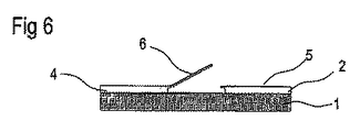
図6は、図1iに示される回路基板から生じ得るような回路基板の実施例を示す。この目的のために、さらなる方法ステップにおいては、可撓領域に対応する凸縁6が被覆層4の面から離れるように曲げられた。凸縁6の可撓性は、切欠き50(図3を参照)を実現することによって外方に曲げられる前に向上させることができる。さらに、被覆層4のうち一層薄い残留物も、曲げ軸の領域において除去することができる。
FIG. 6 shows an embodiment of a circuit board that may result from the circuit board shown in FIG. 1i. For this purpose, in a further method step, the
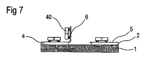
図7に示される実施例においては、凸縁6は、被覆層4に対して垂直になるような程度にまで被覆層4の面から離れるように曲げられている。これにより、3方の空間方向すべて(x、y、z)に向けられた要素40を回路基板上に配置することができるようになる。この場合、要素40zは、早ければ層間剥離層3を除去する前または凸縁6を外方に曲げる前に搭載することができる。既にz次元において形成されている構成要素に対してこのような要素を実際に適合させるのに不可避となり得るプロセス・技術に関する課題が、こうして回避される。要素40は、たとえば、方向依存性センサ、インジケータまたはアクチュエータであってもよい。さらに、図示される配置により、たとえば、3方すべての空間方向への移動を検知することが可能になる。
In the embodiment shown in FIG. 7, the
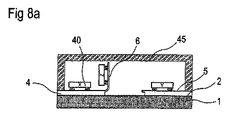
図8aおよび図8bは、いずれの場合にも覆い45を付加的に含む回路基板の2つの実施例を示す。 Figures 8a and 8b show two examples of circuit boards that additionally include a covering 45 in either case.
図8aは、図7からの構成要素を示しており、当該構成要素は、また、覆い45によって3つの要素40すべてを完全に囲んでいる。図8bが示すさらなる実施例は、単に回路基板の部分領域のみを囲んでいる覆い45によって囲まれる2つの要素40しか備えていない。
FIG. 8 a shows the components from FIG. 7, which also completely encloses all three
図9は、凸縁6がその元の位置から180°曲げられている回路基板の具体的な実施例を示す。この結果、凸縁6は回路基板の外端縁を越えて延在する。この結果、凸縁6は、ここでは、たとえば電気的な相互接続用の外部接続部として利用することもできる。このように、一例として、他の回路基板への接続部を単純な態様で設けることができる。さらに、凸縁6はまた、加熱フィルム、アンテナ、容量性または誘導性トランスミッタ/レシーバとして利用することもできる。
FIG. 9 shows a specific embodiment of a circuit board in which the
図10a〜図10cは、製造方法のさらなる変形例を示す。図10aは、回路担体1と、その上に配置された第2の金属化層2とを示す。図10bは、窪み8を有する回路基板を示す。この回路基板は、たとえば窪み8をフライス削りまたはエッチングすることによって、図10aに示されるような回路基板からを製造されてもよい。しかしながら、窪み8は、たとえばレーザ技術を用いて設けることもできる。図1cに示される回路基板も、第1の金属化層5を備えた被覆層4を付加的に有している。被覆層4が第2の金属化層2としか接しておらず、予め設けられている窪み8には突出ていないために、窪み8により空き空間7が形成される。したがって、この製造方法においては、空き空間7が設けられるが、この場合、この目的のために特別に犠牲層を貼り付けることもなく、この犠牲層を後に再び除去する必要もない。第1の金属化層5の被覆層4は、たとえば第2の金属化層2上に積層され得る。被覆層4が窪み8に流れ込まないようにするために、いわゆるノーフロー積層物を、たとえば被覆層4に使用することができる。このようなノーフロー積層物は、たとえば樹脂またはエポキシドを基に製造することができる。これらはさらに、補強のために、安定化組織または他の補強要素を含み得る。たとえば、被覆層4に用いることのできる実現可能な一材料として、イソラ(Isola)によるFR406NFが挙げられる。図10cは、被覆層4が上側および下側の両方に貼り付けられている実施例を示す。この対称的な構造により、たとえば、回路基板に生じる歪みが確実に防止される。これらの歪みは、たとえば回路担体1および被覆層4について異なる材料を用いることによって生じる可能性がある。
10a to 10c show a further modification of the manufacturing method. FIG. 10a shows a
図11a〜図11dにおいては、さまざまなプロセス段階にある回路基板の可撓領域10を、いずれの場合も平面図で概略的に示している。図11aは、被覆層4および第1の金属化層5が上に貼り付けられている可撓領域10を示す。この場合、第1の金属化層5は、導体トラックおよび接触区域9を形成するよう形づくられる。図11bにおいては、第1の金属化層5の接触区域9が位置している領域の可撓性は、切欠き50によって高められている。切欠き50は、たとえばレーザを用いて設けることができる。しかしながら、接触区域が位置している領域における被覆層4の可撓性がここでは依然として制限されている。というのも、これらの部分領域がそれぞれ、依然として角部によって周囲に接続されているからである。これにより、既に可撓性を有する部分領域に対しても一定の安定性が与えられる。これにより、図11cに図示のとおり、電子部品55を回路基板の可撓領域10上に配置し、かつ接触区域9を介して電気的に接触させることが可能になる。はんだペーストも、たとえばこの目的に用いることができる。明瞭にするために、電子部品55は輪郭だけが示されている。図11dに図示のとおり、電子部品55を配置した後、さらなる切欠き60が設けられる。これらのさらなる切欠きにより、接触区域9が位置している可撓領域は、このときにはもはや、角部によってそれらの周囲には連結されていない。これらの部分領域の可撓性は、付加的な切欠き60によっても大幅に高められた。結果として、電子部品55は、非常に可撓性の高い要素を介してのみ回路基板に接続される。切欠き50および60により、さらには導体トラックの湾曲した経路により、回路基板面方向への引張応力に対する可撓領域10の可撓性が、さらに高められる。
In FIGS. 11a to 11d, the
電子部品55と接触区域9とを接触させるための好ましい方法として、金属性の接続バンプ(スタッドバンプ)を用いたはんだ付け、導電性接着、サーモソニックボンディング、および熱圧着が挙げられる。この場合、最初に述べた2つの方法は、可撓性のある接触区域9上では何の問題もなく実行することができる。最後に述べた2つの方法は、好ましくは、可撓領域10が依然として層間剥離層3によって支持される限り採用される。というのも、この場合、相当な垂直力が作用するからである。
Preferred methods for bringing the
さらなる実施例(図としては例示せず)を以下に説明する。
回路基板はまた、両端に可撓領域10を有する回路担体1を含み得る。
Further embodiments (not shown in the figure) are described below.
The circuit board may also include a
さらなる実施例においては、回路基板は、層間剥離層3と被覆層4との間に配置された障壁層を付加的に含む。上記障壁層は、たとえば、レジストまたは金属を含み得る。このような付加的な障壁層は、層間剥離層3上で被覆層4を硬化させている間、この被覆層4に及ぼされる可能性のある影響を防止することができる。
In a further embodiment, the circuit board additionally includes a barrier layer disposed between the
さらなる実施例においては、層間剥離層3は、回路基板において形成されるが、再び除去されることはない。一例として、被覆層4が固着していない材料を、回路基板に残留する層間剥離層3のために使用することができる。一例として、PTFEなどのフッ素化ポリマーをこの目的のために使用することができる。層間剥離層3とその上に配置された被覆層4との間が接着されていないために、可撓領域10は、被覆層4の面から、層間剥離層3とは反対向きの方向に移動させることができる。さらに、可撓領域はまた、曲げたり圧縮したりすることにより、回路基板面の方向に作用する圧縮応力を受けて降伏する可能性がある。
In a further embodiment, the
さらなる実施例においては、可撓領域10は第1の金属化層5だけを含んでおり、被覆層4は含んでいない。しかしながら、第1の金属化層5は、その上側にある付加的な層によって安定させることができる。対応する接触区域は第1の金属化層5の下方に位置しており、その接触区域は、たとえば第2の金属化層2に形づくることができる。対応する接触区域は、可撓領域10が押し込まれると、第1の金属化層5または接触区域9として具体化された領域と、対応する接触区域との間に導電性接点を設けることができるように配置される。たとえば、押しボタン式スイッチをこのようにして製造することができる。
In a further embodiment, the
可撓領域10は、また、複数の第1の金属化層5を含み得る。これらの複数の第1の金属化層5は、たとえば、それらの間に位置する複数の被覆層4によって分離することができる。この場合、各々の第1の金属化層5は、異なる形にされてもよい。したがって、一例としては、図11に示される4つの導体トラックが4つの異なる面に位置し得る。
The
構成要素と回路基板との組合せが存在するが、現在のところ、ボンディングワイヤまたは他の何らかの可撓性接続によってのみ構成要素と接触させることができる。これは、たとえば回路基板上において構成要素を直接はんだ付けするといった固定された接続の場合に、過度に高い機械的応力が構成要素において生じる可能性があるからである。本発明の対応する実施例でも、接点が可撓領域における回路基板上に位置していれば、剛性接続によってこのような構成要素を回路基板に連結することが可能となる。可撓領域は、それが貼り付けられている構成要素には応力を生じさせないという効果を有する。 There are combinations of components and circuit boards, but currently they can only be brought into contact with the components by means of bonding wires or some other flexible connection. This is because excessively high mechanical stresses can occur in the component in the case of a fixed connection, for example soldering the component directly on the circuit board. Corresponding embodiments of the present invention also allow such components to be coupled to the circuit board by a rigid connection if the contacts are located on the circuit board in the flexible region. The flexible region has the effect of not causing stress on the component to which it is attached.
空き空間7が空隙として形成されている実施例においては、特定の一実施例において、空隙が軟質な物質またはゼラチン状の物質で満たされており、このため、空隙に押し込まれる可撓領域10が、安定化されるかまたははね返るようにされる。
In an embodiment in which the
本発明は、具体的な実施例に基づいた説明には限定されない。むしろ、本発明は、いかなる新規な特徴、および、特に特許請求の範囲における特徴の如何なる組合せをも含む特徴の如何なる組合せをも、この特徴またはこの組合せ自体が特許請求の範囲または具体的な実施例において明確に規定されていなくても、包含している。 The present invention is not limited to the description based on the specific embodiments. Rather, the present invention contemplates any novel features, and in particular any combination of features, including any combination of the features in the claims, whether the features or the combinations themselves are within the scope of the claims or specific embodiments. It is included even if it is not clearly defined in.
1 回路担体、2 第2の金属化層、3 層間剥離層、4 被覆層、5 第1の金属化層、6 凸縁、7 空き空間、8 窪み、9 接触区域、10 可撓領域、15 マスク、20a 開口部、20b トレンチ、25a 入口、25b 出口、30 電子部品、35 チャネル、40 要素、45 覆い、50 切欠き、55 電子部品、60 さらなる切欠き。
DESCRIPTION OF
Claims (19)
回路担体(1)と、
非導電性材料からできており、有機物質を含み、回路担体(1)上に配置される被覆層(4)と、
少なくとも部分的に被覆層(4)上に配置される第1の金属化層(5)とを含み、
前記第1の金属化層(5)は可撓領域(10)を有する、回路基板。 A circuit board,
A circuit carrier (1);
A coating layer (4) made of a non-conductive material, comprising an organic substance and disposed on the circuit carrier (1);
A first metallization layer (5) disposed at least partially on the covering layer (4),
The circuit board, wherein the first metallization layer (5) has a flexible region (10).
回路担体(1)を設けるステップと、
回路担体(1)のうち空間的に区切られた部分領域に対して層間剥離層(3)を貼り付けるステップと、
回路担体(1)の部分領域および層間剥離層(3)に対して層シーケンスを施すステップとを含み、前記層シーケンスは、
有機材料を含む被覆層(4)と、
被覆層(16)上における第1の金属化層(5)とを含み、前記方法はさらに、
被覆層(4)および第1の金属化層(5)を構造化するステップを含み、
第1の金属化層(5)の可撓領域(10)が規定される、方法。 A method for manufacturing a circuit board, comprising:
Providing a circuit carrier (1);
Attaching the delamination layer (3) to a spatially partitioned partial region of the circuit carrier (1);
Applying a layer sequence to a partial region of the circuit carrier (1) and the delamination layer (3), the layer sequence comprising:
A coating layer (4) comprising an organic material;
A first metallization layer (5) on the covering layer (16), the method further comprising:
Structuring the covering layer (4) and the first metallization layer (5),
Method wherein the flexible region (10) of the first metallization layer (5) is defined.
回路担体(1)を設けるステップと、
回路担体(1)における窪み(8)を加工するステップと、
窪み(8)を覆うものの充填せず、結果として空き空間(7)を形成するように回路担体(1)に層シーケンスを施すステップとを含み、前記層シーケンスは、有機材料を含む被覆層(4)と、被覆層(4)上における第1の金属化層(5)とを含み、前記方法はさらに、
第1の金属化層(5)の可撓領域(10)が形成されるように空き空間(7)の上方に被覆層(4)および第1の金属化層(5)を構造化するステップを含む、方法。 A method for manufacturing a circuit board, comprising:
Providing a circuit carrier (1);
Machining the recess (8) in the circuit carrier (1);
Applying a layer sequence to the circuit carrier (1) so as to form a vacant space (7) without covering what is covered by the depression (8), the layer sequence comprising a coating layer comprising an organic material ( 4) and a first metallization layer (5) on the coating layer (4), the method further comprising:
Structuring the cover layer (4) and the first metallization layer (5) above the empty space (7) so that a flexible region (10) of the first metallization layer (5) is formed. Including a method.
Applications Claiming Priority (3)
| Application Number | Priority Date | Filing Date | Title |
|---|---|---|---|
| DE102008028300.2A DE102008028300B4 (en) | 2008-06-13 | 2008-06-13 | Flexible area printed circuit board and method of manufacture |
| DE102008028300.2 | 2008-06-13 | ||
| PCT/EP2009/057051 WO2009150133A1 (en) | 2008-06-13 | 2009-06-08 | Circuit board with a flexible region and method for production thereof |
Publications (2)
| Publication Number | Publication Date |
|---|---|
| JP2011523223A true JP2011523223A (en) | 2011-08-04 |
| JP2011523223A5 JP2011523223A5 (en) | 2012-06-28 |
Family
ID=41058975
Family Applications (1)
| Application Number | Title | Priority Date | Filing Date |
|---|---|---|---|
| JP2011512955A Pending JP2011523223A (en) | 2008-06-13 | 2009-06-08 | Circuit board with flexible region and method for manufacturing the same |
Country Status (4)
| Country | Link |
|---|---|
| US (1) | US9035189B2 (en) |
| JP (1) | JP2011523223A (en) |
| DE (1) | DE102008028300B4 (en) |
| WO (1) | WO2009150133A1 (en) |
Cited By (1)
| Publication number | Priority date | Publication date | Assignee | Title |
|---|---|---|---|---|
| JP2018515925A (en) * | 2015-05-07 | 2018-06-14 | コンティ テミック マイクロエレクトロニック ゲゼルシャフト ミット ベシュレンクテル ハフツングConti Temic microelectronic GmbH | Printed circuit board and method for manufacturing printed circuit board |
Families Citing this family (6)
| Publication number | Priority date | Publication date | Assignee | Title |
|---|---|---|---|---|
| DE102010034718B4 (en) | 2010-08-18 | 2017-11-30 | Deutsches Zentrum für Luft- und Raumfahrt e.V. | Stretchable substrate having a contact point between a polymer-based electrical conductor and another electrical conductor |
| JP5880428B2 (en) * | 2012-12-28 | 2016-03-09 | 株式会社オートネットワーク技術研究所 | Card edge connector |
| US20170027070A1 (en) * | 2015-07-23 | 2017-01-26 | Magna Closures Inc. | Housing assembly of a power operated device and method of manufacturing thereof |
| EP3454312B1 (en) * | 2017-09-11 | 2019-08-07 | Siemens Schweiz AG | Optical smoke alarm with a pivotable conductor plate section with a light transmitter and/or receiver arranged on same |
| EP3562279A1 (en) * | 2018-04-25 | 2019-10-30 | Siemens Aktiengesellschaft | Production of an electrical connection of components with a contacting plate |
| DE102019201281B4 (en) * | 2019-01-31 | 2022-07-07 | Fraunhofer-Gesellschaft zur Förderung der angewandten Forschung e.V. | Support arrangement and method for producing a support arrangement |
Citations (5)
| Publication number | Priority date | Publication date | Assignee | Title |
|---|---|---|---|---|
| JPS58153468U (en) * | 1982-04-08 | 1983-10-14 | 株式会社フジクラ | flexible printed circuit board |
| JPS6268265U (en) * | 1985-10-18 | 1987-04-28 | ||
| JP2004140018A (en) * | 2002-10-15 | 2004-05-13 | Denso Corp | Process for producing multilayer board, multilayer board, and mobile apparatus using it |
| JP2006216436A (en) * | 2005-02-04 | 2006-08-17 | Fujikura Ltd | Packaging method of lighting system and light source for lighting |
| JP2006342238A (en) * | 2005-06-08 | 2006-12-21 | Kyocera Chemical Corp | Thermosetting adhesive sheet, copper-clad laminate and flexible printed wiring board |
Family Cites Families (40)
| Publication number | Priority date | Publication date | Assignee | Title |
|---|---|---|---|---|
| FR2475804A1 (en) * | 1980-02-12 | 1981-08-14 | Lewiner Jacques | IMPROVEMENTS ON COMPOSITE SHEETS CONSTITUTING ELECTROMECHANICAL TRANSDUCERS AND TRANSDUCERS EQUIPPED WITH SUCH SHEETS |
| JPS58153468A (en) | 1982-03-05 | 1983-09-12 | Sharp Corp | Program reserving device of television receiver |
| AU572615B2 (en) * | 1983-12-27 | 1988-05-12 | Sony Corporation | Electrically conductive adhesive sheet circuit board and electrical connection structure |
| JPS6268265A (en) | 1985-09-19 | 1987-03-28 | Kawasaki Steel Corp | Grinding method for steel strip surface flaw |
| US4990948A (en) * | 1986-12-27 | 1991-02-05 | Canon Kabushiki Kaisha | Flexible printed circuit board |
| US5103375A (en) * | 1990-02-05 | 1992-04-07 | Motorola, Inc. | Electronic module assembly and method of manufacture |
| US5159751A (en) * | 1990-02-05 | 1992-11-03 | Motorola, Inc. | Method of manufacturing electronic module assembly |
| JP2875076B2 (en) * | 1990-11-29 | 1999-03-24 | 三井化学株式会社 | Flexible wiring board |
| JP2801487B2 (en) * | 1992-04-30 | 1998-09-21 | シャープ株式会社 | Panel mounting structure, mounting method, and resin supply curing method |
| US5428190A (en) * | 1993-07-02 | 1995-06-27 | Sheldahl, Inc. | Rigid-flex board with anisotropic interconnect and method of manufacture |
| DE4341103C1 (en) * | 1993-12-02 | 1995-01-12 | Harting Elektronik Gmbh | Electrical plug connector |
| EP0835497B1 (en) * | 1995-06-27 | 2013-03-27 | Morpho Cards GmbH | Chip card |
| JPH09331153A (en) | 1996-06-11 | 1997-12-22 | Toshiba Chem Corp | Manufacture of multilayer flexible wiring board |
| DE19720106C2 (en) * | 1997-05-16 | 2001-03-15 | Telefunken Microelectron | Device for receiving electrical components |
| DE50002850D1 (en) * | 1999-05-31 | 2003-08-14 | Tyco Electronics Logistics Ag | INTELLIGENT POWER MODULE |
| FI112644B (en) * | 2000-11-10 | 2003-12-31 | Vaisala Oyj | Surface micromechanical absolute pressure sensor and method of manufacture thereof |
| AUPR846701A0 (en) | 2001-10-25 | 2001-11-15 | Microtechnology Centre Management Limited | A method of fabrication of micro-devices |
| DE10206818A1 (en) * | 2002-02-18 | 2003-08-28 | Infineon Technologies Ag | Electronic component used as a semiconductor chip comprises an electrically conducting adhesive layer between the metallic surfaces of components of the electronic component |
| DE20221189U1 (en) | 2002-09-19 | 2005-05-19 | Ruwel Ag | Printed circuit board with at least one rigid area and at least one flexible area |
| US7371970B2 (en) | 2002-12-06 | 2008-05-13 | Flammer Jeffrey D | Rigid-flex circuit board system |
| US20040145874A1 (en) | 2003-01-23 | 2004-07-29 | Stephane Pinel | Method, system, and apparatus for embedding circuits |
| WO2004077898A2 (en) * | 2003-02-26 | 2004-09-10 | Wavezero Inc. | Methods and devices for connecting and grounding an emi shield to a printed circuit board |
| CN100454533C (en) * | 2003-04-15 | 2009-01-21 | 波零公司 | EMI shielding for electronic component packaging |
| US20040232535A1 (en) * | 2003-05-22 | 2004-11-25 | Terry Tarn | Microelectromechanical device packages with integral heaters |
| DE10345257B4 (en) * | 2003-09-29 | 2008-10-02 | Infineon Technologies Ag | Chip card with contact fields and method for producing such contact fields |
| JP3722223B2 (en) * | 2003-10-27 | 2005-11-30 | セイコーエプソン株式会社 | Semiconductor device and manufacturing method thereof, electronic module, and electronic apparatus |
| US7176600B2 (en) * | 2003-12-18 | 2007-02-13 | Palo Alto Research Center Incorporated | Poling system for piezoelectric diaphragm structures |
| EP1737564B1 (en) * | 2004-03-12 | 2019-09-11 | SRI International | Mechanical meta-materials |
| DE102004028211A1 (en) | 2004-06-09 | 2005-12-29 | Robert Bosch Gmbh | Circuit board made from epoxy resin for chip structures comprises fixing sections for holding the circuit board, a fixing section in which components are soldered and a structure for changing the board stiffness |
| JP4536430B2 (en) * | 2004-06-10 | 2010-09-01 | イビデン株式会社 | Flex rigid wiring board |
| JP2006019636A (en) * | 2004-07-05 | 2006-01-19 | Renesas Technology Corp | Semiconductor apparatus |
| US20060040091A1 (en) * | 2004-08-23 | 2006-02-23 | Bletsos Ioannis V | Breathable low-emissivity metalized sheets |
| US7312401B2 (en) * | 2004-09-21 | 2007-12-25 | Ibiden Co., Ltd. | Flexible printed wiring board |
| JP4306590B2 (en) * | 2004-11-05 | 2009-08-05 | セイコーエプソン株式会社 | Electro-optical device and electronic apparatus |
| US7274107B2 (en) * | 2005-01-21 | 2007-09-25 | Infineon Technologies Ag | Semiconductor device |
| JP2006231174A (en) | 2005-02-23 | 2006-09-07 | Matsushita Electric Works Ltd | Organic-material treatment apparatus |
| JP4534972B2 (en) * | 2005-03-30 | 2010-09-01 | エプソンイメージングデバイス株式会社 | Electro-optical device and electronic apparatus |
| JP4095082B2 (en) * | 2005-08-31 | 2008-06-04 | Tdk株式会社 | Flexible wiring board for magnetic head assembly |
| US7388756B1 (en) | 2006-12-12 | 2008-06-17 | The Boeing Company | Method and system for angled RF connection using a flexible substrate |
| KR20090070916A (en) * | 2007-12-27 | 2009-07-01 | 삼성전기주식회사 | Semiconductor device and manufacturing method thereof |
-
2008
- 2008-06-13 DE DE102008028300.2A patent/DE102008028300B4/en active Active
-
2009
- 2009-06-08 US US12/997,867 patent/US9035189B2/en active Active
- 2009-06-08 JP JP2011512955A patent/JP2011523223A/en active Pending
- 2009-06-08 WO PCT/EP2009/057051 patent/WO2009150133A1/en active Application Filing
Patent Citations (5)
| Publication number | Priority date | Publication date | Assignee | Title |
|---|---|---|---|---|
| JPS58153468U (en) * | 1982-04-08 | 1983-10-14 | 株式会社フジクラ | flexible printed circuit board |
| JPS6268265U (en) * | 1985-10-18 | 1987-04-28 | ||
| JP2004140018A (en) * | 2002-10-15 | 2004-05-13 | Denso Corp | Process for producing multilayer board, multilayer board, and mobile apparatus using it |
| JP2006216436A (en) * | 2005-02-04 | 2006-08-17 | Fujikura Ltd | Packaging method of lighting system and light source for lighting |
| JP2006342238A (en) * | 2005-06-08 | 2006-12-21 | Kyocera Chemical Corp | Thermosetting adhesive sheet, copper-clad laminate and flexible printed wiring board |
Cited By (2)
| Publication number | Priority date | Publication date | Assignee | Title |
|---|---|---|---|---|
| JP2018515925A (en) * | 2015-05-07 | 2018-06-14 | コンティ テミック マイクロエレクトロニック ゲゼルシャフト ミット ベシュレンクテル ハフツングConti Temic microelectronic GmbH | Printed circuit board and method for manufacturing printed circuit board |
| US10251276B2 (en) | 2015-05-07 | 2019-04-02 | Conti Temic Microelectronic Gmbh | Printed circuit board and a method for producing a printed circuit board |
Also Published As
| Publication number | Publication date |
|---|---|
| WO2009150133A1 (en) | 2009-12-17 |
| DE102008028300A1 (en) | 2009-12-24 |
| US9035189B2 (en) | 2015-05-19 |
| DE102008028300B4 (en) | 2021-10-07 |
| US20110214905A1 (en) | 2011-09-08 |
Similar Documents
| Publication | Publication Date | Title |
|---|---|---|
| JP2011523223A (en) | Circuit board with flexible region and method for manufacturing the same | |
| EP1740025B1 (en) | Wiring board and method for manufacturing the same | |
| US9867296B2 (en) | Printed circuit board and package substrate | |
| JP5168838B2 (en) | Multilayer printed wiring board and manufacturing method thereof | |
| TWI495075B (en) | Interconnect structure | |
| TWI389608B (en) | Component built-in wiring substrate and manufacturing method thereof | |
| US8692363B2 (en) | Electric part package and manufacturing method thereof | |
| JP5219276B2 (en) | Manufacturing method of printed circuit board with built-in electronic elements | |
| JP5191889B2 (en) | Manufacturing method of component built-in wiring board | |
| JP5093353B2 (en) | Manufacturing method of component built-in module and component built-in module | |
| JP2004538641A (en) | Electronic component having synthetic resin housing and method of manufacturing the same | |
| JP2008198999A (en) | Printed circuit board with built-in electronic device and method of manufacturing the same | |
| JP2019519930A (en) | Module and method for manufacturing multiple modules | |
| JP4447143B2 (en) | Semiconductor device and manufacturing method thereof | |
| JP2009246315A (en) | Substrate incorporating component and mounting structure | |
| KR20090096809A (en) | Method of manufacturing semiconductor chip embedded printed circuit board | |
| JP2005302922A (en) | Wiring board and its manufacturing method | |
| JP2008053693A (en) | Semiconductor module, portable device, and manufacturing method of semiconductor module | |
| KR101417264B1 (en) | The printed circuit board and the method for manufacturing the same | |
| JP2013540368A (en) | Printed circuit board and manufacturing method thereof | |
| KR100582145B1 (en) | Manufacturing method of semiconductor device | |
| JP4597561B2 (en) | Wiring board and manufacturing method thereof | |
| CN111385971B (en) | Circuit board and method for manufacturing the same | |
| JP5150720B2 (en) | Manufacturing method of electronic assembly and electronic assembly | |
| JP4990492B2 (en) | Semiconductor device |
Legal Events
| Date | Code | Title | Description |
|---|---|---|---|
| A521 | Written amendment |
Free format text: JAPANESE INTERMEDIATE CODE: A523 Effective date: 20120510 |
|
| A621 | Written request for application examination |
Free format text: JAPANESE INTERMEDIATE CODE: A621 Effective date: 20120510 |
|
| A977 | Report on retrieval |
Free format text: JAPANESE INTERMEDIATE CODE: A971007 Effective date: 20130108 |
|
| A131 | Notification of reasons for refusal |
Free format text: JAPANESE INTERMEDIATE CODE: A131 Effective date: 20130115 |
|
| A601 | Written request for extension of time |
Free format text: JAPANESE INTERMEDIATE CODE: A601 Effective date: 20130411 |
|
| A602 | Written permission of extension of time |
Free format text: JAPANESE INTERMEDIATE CODE: A602 Effective date: 20130418 |
|
| A521 | Written amendment |
Free format text: JAPANESE INTERMEDIATE CODE: A523 Effective date: 20130614 |
|
| A131 | Notification of reasons for refusal |
Free format text: JAPANESE INTERMEDIATE CODE: A131 Effective date: 20140107 |
|
| A521 | Written amendment |
Free format text: JAPANESE INTERMEDIATE CODE: A523 Effective date: 20140404 |
|
| A02 | Decision of refusal |
Free format text: JAPANESE INTERMEDIATE CODE: A02 Effective date: 20140909 |