JP2011520249A - Method for etching carbon nanotube film used in non-volatile memory - Google Patents
Method for etching carbon nanotube film used in non-volatile memory Download PDFInfo
- Publication number
- JP2011520249A JP2011520249A JP2011504204A JP2011504204A JP2011520249A JP 2011520249 A JP2011520249 A JP 2011520249A JP 2011504204 A JP2011504204 A JP 2011504204A JP 2011504204 A JP2011504204 A JP 2011504204A JP 2011520249 A JP2011520249 A JP 2011520249A
- Authority
- JP
- Japan
- Prior art keywords
- etching
- cnt
- layer
- substrate
- bcl
- Prior art date
- Legal status (The legal status is an assumption and is not a legal conclusion. Google has not performed a legal analysis and makes no representation as to the accuracy of the status listed.)
- Pending
Links
Images
Classifications
-
- H—ELECTRICITY
- H10—SEMICONDUCTOR DEVICES; ELECTRIC SOLID-STATE DEVICES NOT OTHERWISE PROVIDED FOR
- H10N—ELECTRIC SOLID-STATE DEVICES NOT OTHERWISE PROVIDED FOR
- H10N70/00—Solid-state devices having no potential barriers, and specially adapted for rectifying, amplifying, oscillating or switching
- H10N70/20—Multistable switching devices, e.g. memristors
-
- H—ELECTRICITY
- H10—SEMICONDUCTOR DEVICES; ELECTRIC SOLID-STATE DEVICES NOT OTHERWISE PROVIDED FOR
- H10P—GENERIC PROCESSES OR APPARATUS FOR THE MANUFACTURE OR TREATMENT OF DEVICES COVERED BY CLASS H10
- H10P50/00—Etching of wafers, substrates or parts of devices
- H10P50/20—Dry etching; Plasma etching; Reactive-ion etching
- H10P50/28—Dry etching; Plasma etching; Reactive-ion etching of insulating materials
- H10P50/286—Dry etching; Plasma etching; Reactive-ion etching of insulating materials of organic materials
- H10P50/287—Dry etching; Plasma etching; Reactive-ion etching of insulating materials of organic materials by chemical means
-
- B—PERFORMING OPERATIONS; TRANSPORTING
- B82—NANOTECHNOLOGY
- B82Y—SPECIFIC USES OR APPLICATIONS OF NANOSTRUCTURES; MEASUREMENT OR ANALYSIS OF NANOSTRUCTURES; MANUFACTURE OR TREATMENT OF NANOSTRUCTURES
- B82Y10/00—Nanotechnology for information processing, storage or transmission, e.g. quantum computing or single electron logic
-
- B—PERFORMING OPERATIONS; TRANSPORTING
- B82—NANOTECHNOLOGY
- B82Y—SPECIFIC USES OR APPLICATIONS OF NANOSTRUCTURES; MEASUREMENT OR ANALYSIS OF NANOSTRUCTURES; MANUFACTURE OR TREATMENT OF NANOSTRUCTURES
- B82Y40/00—Manufacture or treatment of nanostructures
-
- H—ELECTRICITY
- H10—SEMICONDUCTOR DEVICES; ELECTRIC SOLID-STATE DEVICES NOT OTHERWISE PROVIDED FOR
- H10B—ELECTRONIC MEMORY DEVICES
- H10B63/00—Resistance change memory devices, e.g. resistive RAM [ReRAM] devices
- H10B63/20—Resistance change memory devices, e.g. resistive RAM [ReRAM] devices comprising selection components having two electrodes, e.g. diodes
-
- H—ELECTRICITY
- H10—SEMICONDUCTOR DEVICES; ELECTRIC SOLID-STATE DEVICES NOT OTHERWISE PROVIDED FOR
- H10B—ELECTRONIC MEMORY DEVICES
- H10B63/00—Resistance change memory devices, e.g. resistive RAM [ReRAM] devices
- H10B63/80—Arrangements comprising multiple bistable or multi-stable switching components of the same type on a plane parallel to the substrate, e.g. cross-point arrays
- H10B63/84—Arrangements comprising multiple bistable or multi-stable switching components of the same type on a plane parallel to the substrate, e.g. cross-point arrays arranged in a direction perpendicular to the substrate, e.g. 3D cell arrays
-
- H—ELECTRICITY
- H10—SEMICONDUCTOR DEVICES; ELECTRIC SOLID-STATE DEVICES NOT OTHERWISE PROVIDED FOR
- H10B—ELECTRONIC MEMORY DEVICES
- H10B99/00—Subject matter not provided for in other groups of this subclass
- H10B99/14—Subject matter not provided for in other groups of this subclass comprising memory cells that only have passive resistors or passive capacitors
-
- H—ELECTRICITY
- H10—SEMICONDUCTOR DEVICES; ELECTRIC SOLID-STATE DEVICES NOT OTHERWISE PROVIDED FOR
- H10N—ELECTRIC SOLID-STATE DEVICES NOT OTHERWISE PROVIDED FOR
- H10N70/00—Solid-state devices having no potential barriers, and specially adapted for rectifying, amplifying, oscillating or switching
- H10N70/011—Manufacture or treatment of multistable switching devices
- H10N70/061—Shaping switching materials
- H10N70/063—Shaping switching materials by etching of pre-deposited switching material layers, e.g. lithography
-
- H—ELECTRICITY
- H10—SEMICONDUCTOR DEVICES; ELECTRIC SOLID-STATE DEVICES NOT OTHERWISE PROVIDED FOR
- H10N—ELECTRIC SOLID-STATE DEVICES NOT OTHERWISE PROVIDED FOR
- H10N70/00—Solid-state devices having no potential barriers, and specially adapted for rectifying, amplifying, oscillating or switching
- H10N70/801—Constructional details of multistable switching devices
- H10N70/821—Device geometry
- H10N70/826—Device geometry adapted for essentially vertical current flow, e.g. sandwich or pillar type devices
-
- H—ELECTRICITY
- H10—SEMICONDUCTOR DEVICES; ELECTRIC SOLID-STATE DEVICES NOT OTHERWISE PROVIDED FOR
- H10N—ELECTRIC SOLID-STATE DEVICES NOT OTHERWISE PROVIDED FOR
- H10N70/00—Solid-state devices having no potential barriers, and specially adapted for rectifying, amplifying, oscillating or switching
- H10N70/801—Constructional details of multistable switching devices
- H10N70/881—Switching materials
- H10N70/884—Switching materials based on at least one element of group IIIA, IVA or VA, e.g. elemental or compound semiconductors
- H10N70/8845—Carbon or carbides
-
- H—ELECTRICITY
- H10—SEMICONDUCTOR DEVICES; ELECTRIC SOLID-STATE DEVICES NOT OTHERWISE PROVIDED FOR
- H10P—GENERIC PROCESSES OR APPARATUS FOR THE MANUFACTURE OR TREATMENT OF DEVICES COVERED BY CLASS H10
- H10P50/00—Etching of wafers, substrates or parts of devices
- H10P50/20—Dry etching; Plasma etching; Reactive-ion etching
- H10P50/26—Dry etching; Plasma etching; Reactive-ion etching of conductive or resistive materials
- H10P50/264—Dry etching; Plasma etching; Reactive-ion etching of conductive or resistive materials by chemical means
- H10P50/266—Dry etching; Plasma etching; Reactive-ion etching of conductive or resistive materials by chemical means by vapour etching only
- H10P50/267—Dry etching; Plasma etching; Reactive-ion etching of conductive or resistive materials by chemical means by vapour etching only using plasmas
-
- G—PHYSICS
- G11—INFORMATION STORAGE
- G11C—STATIC STORES
- G11C13/00—Digital stores characterised by the use of storage elements not covered by groups G11C11/00, G11C23/00, or G11C25/00
- G11C13/02—Digital stores characterised by the use of storage elements not covered by groups G11C11/00, G11C23/00, or G11C25/00 using elements whose operation depends upon chemical change
- G11C13/025—Digital stores characterised by the use of storage elements not covered by groups G11C11/00, G11C23/00, or G11C25/00 using elements whose operation depends upon chemical change using fullerenes, e.g. C60, or nanotubes, e.g. carbon or silicon nanotubes
-
- Y—GENERAL TAGGING OF NEW TECHNOLOGICAL DEVELOPMENTS; GENERAL TAGGING OF CROSS-SECTIONAL TECHNOLOGIES SPANNING OVER SEVERAL SECTIONS OF THE IPC; TECHNICAL SUBJECTS COVERED BY FORMER USPC CROSS-REFERENCE ART COLLECTIONS [XRACs] AND DIGESTS
- Y10—TECHNICAL SUBJECTS COVERED BY FORMER USPC
- Y10S—TECHNICAL SUBJECTS COVERED BY FORMER USPC CROSS-REFERENCE ART COLLECTIONS [XRACs] AND DIGESTS
- Y10S977/00—Nanotechnology
- Y10S977/70—Nanostructure
- Y10S977/762—Nanowire or quantum wire, i.e. axially elongated structure having two dimensions of 100 nm or less
Landscapes
- Engineering & Computer Science (AREA)
- Chemical & Material Sciences (AREA)
- Nanotechnology (AREA)
- Physics & Mathematics (AREA)
- Crystallography & Structural Chemistry (AREA)
- Manufacturing & Machinery (AREA)
- Condensed Matter Physics & Semiconductors (AREA)
- General Physics & Mathematics (AREA)
- Mathematical Physics (AREA)
- Theoretical Computer Science (AREA)
- Semiconductor Memories (AREA)
- Drying Of Semiconductors (AREA)
Abstract
炭素ベースの可逆抵抗率スイッチング材料に結合されているステアリング素子を含むメモリセルと、そのメモリセルを形成する方法とが提供される。特定の実施形態では、本発明に従う方法は、基板の上に形成されたカーボンナノチューブ(「CNT」)膜をエッチングする方法であって、基板をマスキング層でコーティングすることと、マスキング層をパターニングすることと、パターニングされたマスキング層を通して非酸素ベースの化学的手法を用いてCNT膜をエッチングすることを含む。他の態様も記載されている。 A memory cell including a steering element coupled to a carbon-based reversible resistivity switching material and a method of forming the memory cell are provided. In certain embodiments, the method according to the present invention is a method of etching a carbon nanotube (“CNT”) film formed on a substrate, wherein the substrate is coated with a masking layer and the masking layer is patterned. And etching the CNT film using a non-oxygen based chemical technique through the patterned masking layer. Other embodiments are also described.
Description
本発明は、不揮発性メモリに関し、特に、炭素ベースの記憶素子を含むメモリセルとそれを形成する方法とに関する。 The present invention relates to non-volatile memories, and more particularly to memory cells including carbon-based storage elements and methods of forming the same.
関連出願との相互参照
本願は、あらゆる目的のためにその全体が本願明細書において参照により援用されている、2008年4月11日に出願された「METHODS FOR ETCHING CARBON NANO-TUBE FILMS FOR USE IN NON-VOLATILE MEMORIES 」という米国仮特許出願第61/044,314号(特許文献1)の利益を主張するとともに、2008年7月15日に出願された「METHODS FOR ETCHING CARBON NANO-TUBE FILMS」という米国仮特許出願第61/081,029号(特許文献2)の利益を主張する。
CROSS-REFERENCE TO RELATED APPLICATIONS its entirety for all purposes are hereby incorporated by reference, filed April 11, 2008 "METHODS FOR ETCHING CARBON NANO-TUBE FILMS FOR USE IN NON-VOLATILE MEMORIES "US Provisional Patent Application No. 61 / 044,314 (patent document 1)" claiming the benefit, "METHODS FOR ETCHING CARBON NANO-TUBE FILMS" filed on July 15, 2008 Claims the benefit of US Provisional Patent Application No. 61 / 081,029 (Patent Document 2).
可逆抵抗スイッチング素子から形成される不揮発性メモリが知られている。例えば、あらゆる目的のためにその全体が本願明細書において参照により援用されている、2007年12月31日に出願された「MEMORY CELL THAT EMPLOYS A SELECTIVELY FABRICATED CARBON NANO-TUBE REVERSIBLE RESISTANCE-SWITCHING ELEMENT AND METHODS OF FORMING THE SAME」という米国特許出願第11/968,154号(特許文献3)は、炭素などの、炭素ベースの可逆抵抗率スイッチング材料と直列に結合されたダイオードを含む再書き込み可能な不揮発性メモリセルを記述している。
しかし、再書き込み可能な抵抗率スイッチング材料からメモリ装置を製造することは技術的に難しく、抵抗率スイッチング材料を使用するメモリ装置を形成する改良された方法が望ましい。
Nonvolatile memories formed from reversible resistance switching elements are known. For example, “MEMORY CELL THAT EMPLOYS A SELECTIVELY FABRICATED CARBON NANO-TUBE REVERSIBLE RESISTANCE-SWITCHING ELEMENT AND METHODS, filed Dec. 31, 2007, which is incorporated herein by reference in its entirety for all purposes. US Patent Application No. 11 / 968,154 entitled “OF FORMING THE SAME” is a rewritable non-volatile including a diode coupled in series with a carbon-based reversible resistivity switching material, such as carbon. A memory cell is described.
However, it is technically difficult to fabricate a memory device from a rewritable resistivity switching material, and an improved method of forming a memory device that uses a resistivity switching material is desirable.
本発明の第1の態様において、基板の上に形成されたカーボンナノチューブ(「CNT」)膜をエッチングする方法が提供され、その方法は、基板をマスキング層でコーティングすることと、マスキング層をパターニングすることと、パターニングされたマスキング層を通して非酸素ベースの化学的手法を用いてCNT膜をエッチングすることとを含む。 In a first aspect of the present invention, a method is provided for etching a carbon nanotube (“CNT”) film formed on a substrate, the method comprising coating the substrate with a masking layer and patterning the masking layer. And etching the CNT film using a non-oxygen based chemical technique through the patterned masking layer.
本発明の第2の態様において、メモリセルを形成する方法が提供され、その方法は、基板より上にCNT材料の層を形成することと、三塩化ホウ素(「BCl3 」)およびジクロリン(「Cl2 」)ならびに約50および約150ワットの間の基板バイアス電力を用いてCNT材料をプラズマエッチングチャンバ内でエッチングすることとを含む。 In a second aspect of the invention, a method of forming a memory cell is provided, the method comprising forming a layer of CNT material above a substrate, boron trichloride (“BCl 3 ”) and dichlorine (“ Cl 2 ") and etching the CNT material in a plasma etch chamber using a substrate bias power between about 50 and about 150 Watts.
本発明の第3の態様において、メモリセルを形成する方法が提供され、その方法は、基板より上にCNT材料の層を形成することと、ほとんど垂直の側壁を有するとともにCNT材料のアンダーカットをほとんどあるいは全く有しないようにCNT材料をエッチングするために非酸素ベースの化学的手法を用いることを含む。 In a third aspect of the present invention, a method of forming a memory cell is provided, the method comprising forming a layer of CNT material above a substrate and having an undercut of CNT material having substantially vertical sidewalls. Using non-oxygen based chemical techniques to etch CNT material so that it has little or no.
本発明の他の特徴および態様は、次の詳細な記述、添付されている特許請求の範囲および添付の図面からより充分に明らかになるはずである。
本発明の特徴は添付の図面と関連して考慮される次の詳細な記述からより明らかに理解することができ、図面全体にわたって同じ参照数字は同じ要素を示す。
Other features and aspects of the present invention will become more fully apparent from the following detailed description, the appended claims and the accompanying drawings.
The features of the present invention can be more clearly understood from the following detailed description considered in conjunction with the accompanying drawings, wherein like reference numerals designate like elements throughout the drawings.
CNT、グラフェン、グラフェンの微晶質または他の領域を包含する非晶質炭素、および他の黒鉛状炭素膜などを含むがこれらに限定はされない或る炭素ベースの膜は、マイクロエレクトロニクス不揮発性メモリを形成するために使用され得る抵抗率スイッチング特性を示すことがある。従って、そのような膜は3次元メモリアレイ内に集積化され得る候補である。例えば、CNT材料は、オンおよびオフ状態間の100倍の分離ならびに中間域から高域の抵抗変化を有するメモリスイッチング特性を実験室スケールの装置において示している。オンおよびオフ状態の間のそのような分離の故に、CNT材料は、垂直ダイオード、薄膜トランジスタまたは他のステアリング素子と直列のCNT材料を用いて形成されるメモリセルの実現可能な候補となる。 Certain carbon-based films include, but are not limited to, CNTs, graphene, amorphous carbon including microcrystalline or other regions of graphene, and other graphitic carbon films May exhibit resistivity switching characteristics that may be used to form Thus, such a film is a candidate that can be integrated into a three-dimensional memory array. For example, CNT materials have shown memory switching characteristics in laboratory scale devices with 100 times separation between on and off states and resistance changes from mid to high. Because of such separation between on and off states, CNT material is a viable candidate for a memory cell formed using CNT material in series with a vertical diode, thin film transistor or other steering element.
前述した例では、2つの金属または他の伝導性の層の間に挟まれた炭素ベースの材料から形成される金属−絶縁体−金属(metal-insulator-metal(「MIM」))スタックは、メモリセルのための抵抗変化材料として役立つことができる。さらに、炭素ベースのMIMスタックは、例えば特許文献3に記載されているような読み出し−書き込み可能なメモリ装置を作るためにダイオードまたはトランジスタと直列に統合され得る。 In the example described above, a metal-insulator-metal (“MIM”) stack formed from a carbon-based material sandwiched between two metals or other conductive layers is: It can serve as a resistance change material for a memory cell. In addition, the carbon-based MIM stack can be integrated in series with a diode or transistor to create a read-write memory device such as that described in US Pat.
しかし、メモリセルを形成するためにCNT材料が使用されるとき、堆積または成長させられたCNT材料は、しばしば、多数の山および谷などの顕著な厚さ変化を伴う粗い表面トポグラフィを有する。粗い表面トポグラフィは、メモリセルを形成するときに困難を引き起こし得る。例えば、CNT材料の粗い表面トポグラフィは、下に存在する基板を過剰にエッチングすることなくCNT材料をエッチングすることを困難にし、製造コストを増大させるとともに集積回路においてそれらを使用することに関連する複雑さを増大させることがある。 However, when CNT material is used to form a memory cell, the deposited or grown CNT material often has a rough surface topography with significant thickness changes such as numerous peaks and valleys. Rough surface topography can cause difficulties when forming memory cells. For example, the rough surface topography of CNT materials makes it difficult to etch CNT materials without over-etching the underlying substrate, increasing manufacturing costs and the complexity associated with using them in integrated circuits. May increase.
本発明に従う代表的な方法は、CNT材料から形成される記憶素子を含むメモリセルを形成する。特に、CNT材料は、割合に低いバイアス条件(例えば、約100W)下でプラズマエッチャならびにBCl3 およびCl2 化学的手法を用いてエッチングされ得る。そのような手法を用いてエッチングされたCNT材料は、ほぼ垂直の側壁を有するとともにCNT材料のアンダーカットをほとんどあるいは全く有しないということが観察されている。 An exemplary method according to the present invention forms a memory cell that includes a storage element formed from a CNT material. In particular, CNT material can be etched using a plasma etcher and BCl 3 and Cl 2 chemistry techniques under relatively low bias conditions (eg, about 100 W). It has been observed that CNT material etched using such a technique has substantially vertical sidewalls and little or no undercutting of the CNT material.
少なくとも幾つかの実施形態では、CVD成長手法、コロイダルスプレーオン手法、およびスピンオン手法によって純粋なCNTが堆積させられ得る。さらに、炭素材料堆積法は、ターゲットからのスパッタ堆積、プラズマ増強化学蒸着(plasma-enhanced chemical vapor deposition (「PECVD」))、PVD、CVD、アーク放電手法、およびレーザーアブレーションを含み得るが、これらに限定されない。堆積温度は約300℃から900℃に及び得る。前駆物質ガス源は、ヘキサン、シクロヘキサン、アセチレン、シングルおよびダブル短鎖炭化水素(例えば、メタン)、種々のベンゼンベースの炭化水素、多環芳香族、短鎖エステル、エーテル、アルコール、あるいはそれらの組み合わせを含み得るけれども、それらに限定されない。或る場合には、換算温度での成長を促進するために「シーディング(seeding )」面が使用され得る(例えば、他の厚さが使用され得るけれども、約1〜100オングストロームの鉄(「Fe」)、ニッケル(「Ni」)、コバルト(「Co」)など)。 In at least some embodiments, pure CNTs can be deposited by CVD growth techniques, colloidal spray-on techniques, and spin-on techniques. In addition, carbon material deposition methods may include sputter deposition from a target, plasma-enhanced chemical vapor deposition (“PECVD”), PVD, CVD, arc discharge techniques, and laser ablation. It is not limited. The deposition temperature can range from about 300 ° C to 900 ° C. The precursor gas source is hexane, cyclohexane, acetylene, single and double short chain hydrocarbons (eg methane), various benzene based hydrocarbons, polycyclic aromatics, short chain esters, ethers, alcohols, or combinations thereof Including, but not limited to. In some cases, a “seeding” surface can be used to promote growth at reduced temperatures (eg, about 1 to 100 angstroms of iron (“, although other thicknesses can be used. Fe "), nickel (" Ni "), cobalt (" Co "), etc.).
或る実施形態では、炭素ベースの抵抗率スイッチング材料は、前に言及した手法のいずれかで堆積させられる非晶質炭素、あるいは黒鉛状炭素と混合された誘電体充填材料から構成され得る。この集積化方式の特定の実施形態は、CNT材料のスピンまたはスプレー塗布と、それに続く、炭素ベースのライナ材料として用いられるアプライド・マテリアルズ・インコーポレイテッド(Applied Materials, Inc.) からの非晶質炭素、Producer(登録商標)ツールの堆積とを含む。任意の炭素ベース保護ライナは、CNT材料を堆積させるために使用されるものと同様のあるいは異なる堆積手法を用いて堆積させられ得る。 In some embodiments, the carbon-based resistivity switching material may be composed of a dielectric filler material mixed with amorphous carbon or graphitic carbon deposited by any of the previously mentioned techniques. A particular embodiment of this integration scheme is a spin or spray application of CNT material, followed by an amorphous from Applied Materials, Inc. used as a carbon-based liner material. Carbon, Producer® tool deposition. Any carbon-based protective liner can be deposited using a deposition technique similar to or different from that used to deposit the CNT material.
炭素ベースの抵抗率スイッチング材料は任意の厚さに堆積させられ得る。或る実施形態では、炭素ベース抵抗率スイッチング材料は約1〜1,000オングストロームの間であり得るけれども、他の厚さが使用されてもよい。本願明細書に記載されているものなどのデバイス構成に依存して、好ましい範囲は200〜400オングストローム、400〜600オングストローム、600〜800オングストローム、および800〜1,000オングストロームを含むことができる。 The carbon based resistivity switching material can be deposited to any thickness. In some embodiments, the carbon-based resistivity switching material can be between about 1 and 1,000 angstroms, although other thicknesses may be used. Depending on the device configuration, such as those described herein, preferred ranges can include 200-400 angstroms, 400-600 angstroms, 600-800 angstroms, and 800-1,000 angstroms.
代表的な実施形態
本発明の第1の代表的な実施形態に従って、マイクロエレクトロニクス構造の形成は、底部電極および頂部電極の間に配置されている炭素膜を有するMIMデバイスの形成を含み、炭素膜は、例えば、抵抗率スイッチングCNT層を含む。構造は、誘電体充填ステップ中に炭素ベース材料を劣化から守るために設けられる誘電体側壁ライナをも含む。
Exemplary Embodiments According to a first exemplary embodiment of the present invention, the formation of a microelectronic structure includes the formation of a MIM device having a bottom electrode and a carbon film disposed between the top electrode, and the carbon film Includes, for example, a resistivity-switching CNT layer. The structure also includes a dielectric sidewall liner that is provided to protect the carbon-based material from degradation during the dielectric filling step.
図1は、本発明に従って提供される、メモリセル100とも称される第1の代表的なマイクロエレクトロニクス構造100の横断面立面図である。メモリセル100は、基板(図示せず)の上、例えば基板の上の絶縁層の上に形成された第1の導体102を含む。第1の導体102は、タングステン(「W」)、銅(「Cu」)、アルミニウム(「Al」)、金(「Au」)、または他の金属の層などの、第1の金属層104を含み得る。第1の導体102は、MIM層スタック構造105の下側部分を含むことができ、MIM105の底部電極として機能することができる。窒化タングステン(「WN」)、窒化チタン(「TiN」)、窒化タンタル(「TaN」)、モリブデン(「Mo」)などの接着層106、あるいは類似の層は任意のものであるけれども図1では第1の金属層104の上に形成されて示されている。一般的に、複数の第1の導体102が設けられて(例えば、第1の導体102の各々の間に二酸化ケイ素(「SiO2 」)または他の誘電体材料絶縁を使用することによって)互いから絶縁させられ得る。例えば、第1の導体102は、格子パターニングされたアレイのワード線またはビット線であり得る。
FIG. 1 is a cross-sectional elevation view of a first exemplary
CNT材料108の層が、任意の適切なCNT形成プロセスを用いて第1の導体102の上に形成される。CNT材料108は、MIM層スタック構造105の中央部分を構成してMIM105のスイッチング層として機能することができる。CNT材料108は、種々の手法により堆積させられ得る。1つの手法は、第1の導体102の上にカーボンナノチューブ懸濁液をスプレーコーティングまたはスピンコーティングすることによってランダムなCNT材料を作ることを包含する。他の1つの手法は、CVD、PECVDなどによって基板に固着されたシードからカーボンナノチューブを成長させることを含む。種々のCNT堆積手法についての論議が、特許文献3と、関連する2007年12月31日に出願された「MEMORY CELL THAT EMPLOYS A SELECTIVELY FABRICATED CARBON NANO-TUBE REVERSIBLE RESISTANCE-SWITCHING ELEMENT FORMED OVER A BOTTOM CONDUCTOR AND METHODS OF FORMING THE SAME 」という米国特許出願第11/968,156号(特許文献4)および2007年12月31日に出願された「MEMORY CELL WITH PLANARIZED CARBON NANOTUBE LAYER AND METHODS OF FORMING THE SAME 」という米国特許出願第11/968,159号(特許文献5)とに見出され、これら特許出願はあらゆる目的のためにその全体が本願明細書において参照により援用されている。
A layer of
本発明に従う或る実施形態では、CNT材料108の堆積/形成後に、CNT材料108の特性を改変するためにアニーリングのステップが実行され得る。特に、アニーリングは、真空中あるいは1つ以上のフォーミングガスの存在下で、約350℃から約900℃までの範囲の温度で、約30分から約180分にわたって、実行され得る。アニーリングは、好ましくは、およそ80%(N2 ):20%(H2 )混合物のフォーミングガス中に約625℃で約1時間にわたって実行される。
In certain embodiments according to the present invention, after deposition / formation of the
適切なフォーミングガスはN2 、Ar、およびH2 のうちの1つ以上を含み得るが、好ましいフォーミングガスは約75%より多いN2 またはArと約25%未満のH2とを有する混合物を含み得る。代わりに、真空が使用され得る。適切な温度は約350℃から約900℃に及ぶが、好ましい温度は約585℃から約675℃に及び得る。適切な持続時間は約0.5時間から約3時間に及び得るが、好ましい持続時間は約1時間から約1.5時間に及び得る。適切な圧力は約1mTから約760mTに及び得るが、好ましい圧力は約300mTから約600mTに及び得る。 Suitable forming gases may include one or more of N 2 , Ar, and H 2 , but preferred forming gases include mixtures having greater than about 75% N 2 or Ar and less than about 25% H 2. May be included. Alternatively, a vacuum can be used. Suitable temperatures range from about 350 ° C to about 900 ° C, although preferred temperatures can range from about 585 ° C to about 675 ° C. Suitable durations can range from about 0.5 hours to about 3 hours, but preferred durations can range from about 1 hour to about 1.5 hours. Suitable pressures can range from about 1 mT to about 760 mT, but preferred pressures can range from about 300 mT to about 600 mT.
このアニーリングは、CNT材料108より上の頂部電極の形成の前に実行され得る。アニーリングと電極金属堆積との間の好ましくは約2時間の待ち時間が、アニーリングの使用に好ましくは伴う。ランプアップ持続時間は約0.2時間から約1.2時間に及ぶことができ、好ましくは約0.5時間および0.8時間の間にある。同様に、ランプダウン持続時間も約0.2時間から約1.2時間に及ぶことができ、好ましくは約0.5時間および0.8時間の間にある。
This annealing can be performed prior to the formation of the top electrode above the
いかなる特定の理論にも束縛されたくないけれども、CNT材料は空気から水を吸収するかも知れずかつ/またはCNT材料が形成された後に1つ以上の官能基がCNT材料に付着しているかも知れないと考えられる。ときには有機官能基が堆積前処理のために必要とされる。好ましい官能基の1つはカルボキシル基である。同様に、水分および/または有機官能基は、CNT材料の層割れの可能性を高めるかも知れないと考えられる。さらに、官能基は、例えばクリーニングおよび/またはフィルタリングのプロセスの間にCNT材料に付着し得ると考えられる。炭素形成後のアニーリングは、CNT材料に関連する水分および/またはカルボキシル基もしくは他の官能基を除去することができる。その結果として、或る実施形態では、CNT材料の上での頂部電極の形成前にCNT材料がアニーリングされれば、CNT材料および/または頂部電極材料の基板からの層割れは起こりにくくなる。 Although not wishing to be bound by any particular theory, the CNT material may absorb water from the air and / or one or more functional groups may be attached to the CNT material after the CNT material is formed. It is not considered. Sometimes organic functional groups are required for pre-deposition treatment. One preferred functional group is a carboxyl group. Similarly, it is believed that moisture and / or organic functional groups may increase the likelihood of CNT material cracking. Furthermore, it is believed that the functional groups can attach to the CNT material, for example during a cleaning and / or filtering process. Annealing after carbon formation can remove moisture and / or carboxyl groups or other functional groups associated with the CNT material. As a result, in some embodiments, if the CNT material is annealed prior to formation of the top electrode on the CNT material, layer cracking of the CNT material and / or the top electrode material from the substrate is less likely to occur.
そのようなCNT形成後のアニーリングの組み込みは、CNT材料を含むデバイス上に存在する他の層をも、それらの他の層もアニーリングにさらされることになるので、好ましくは考慮に入れるべきものである。例えば、前述した好ましいアニーリングのパラメータが他の層を損傷させる場合にはアニーリングは省略されてもよく、あるいはそのパラメータが調整されてもよい。アニーリングのパラメータは、アニーリングされるデバイスの層を損傷させることなく水分および/またはカルボキシル基もしくは他の官能基の除去という結果をもたらす範囲の中で調整され得る。例えば、形成されるデバイスの総熱余裕度内に留まるように温度が調整され得る。同様に、特定のデバイスに適する任意の適切なフォーミングガス、温度および/または持続時間が使用され得る。一般的に、そのようなアニーリングは、CNT材料、グラファイト、グラフェン、非晶質炭素などを有する層などの、任意のカーボンベースの層あるいは炭素含有材料に対して使用され得る。 The incorporation of such post-CNT annealing is preferably to be taken into account as other layers present on the device containing the CNT material will also be exposed to annealing. is there. For example, if the preferred annealing parameters described above damage other layers, annealing may be omitted or the parameters may be adjusted. The annealing parameters can be adjusted within a range that results in the removal of moisture and / or carboxyl groups or other functional groups without damaging the layers of the annealed device. For example, the temperature can be adjusted to remain within the total thermal margin of the device being formed. Similarly, any suitable forming gas, temperature and / or duration suitable for a particular device can be used. In general, such annealing can be used for any carbon-based layer or carbon-containing material, such as a layer having CNT material, graphite, graphene, amorphous carbon, and the like.
あらゆる目的のためにその全体が本願明細書において参照により援用されている、「ELECTRONIC DEVICES INCLUDING CARBON-BASED FILMS HAVING SIDEWALL LINERS,AND METHODS OF FORMING SUCH DEVICES」という2009年3月31日に出願された、本発明の譲受人により所有されている同時係属中の米国特許出願第12/415,964号(特許文献6)に記載されているように、本発明に従う或る実施形態では、CNT材料108の堆積/形成の後に、任意の第2の炭素ベース材料層(図示せず)が、CNT材料108を覆う保護ライナとして形成され得る。
Filed on March 31, 2009, "ELECTRONIC DEVICES INCLUDING CARBON-BASED FILMS HAVING SIDEWALL LINERS, AND METHODS OF FORMING SUCH DEVICES", which is incorporated by reference herein in its entirety for all purposes, In certain embodiments according to the present invention, as described in co-pending US patent application Ser. No. 12 / 415,964 owned by the assignee of the present invention, After deposition / formation, an optional second carbon-based material layer (not shown) can be formed as a protective liner over the
CNT材料108の形成後、TiN、TaN、W、WN、タンタルカーボンニトリド(「TaCN」)などの接着/障壁層110がCNT材料108の上に形成され得る。図1に示されているように、接着層110は、スイッチング層としてのCNT材料108と、底部電極としての第1の金属層104および任意の接着層106とを含むMIMデバイス105の頂部電極として機能することができる。それゆえ、次のセクションでは、接着/障壁層110をMIM105の「頂部電極110」と称する。
After formation of the
本発明に従う或る実施形態では、頂部電極110は、例えば同様の材料のPVDに用いられるものよりも低いエネルギーレベルを必要とするものなどの、低エネルギー堆積手法を用いて堆積させられ得る。そのような代表的な堆積手法は、非共形堆積、低バイアス電力物理蒸着(low bias power physical vapor deposition(「LBP−PVD」))、低温PVD、および他の類似の手法を含み得る。炭素材料上に頂部電極110を堆積させるために非共形低エネルギー堆積手法を使用すれば、CNT材料108に対する堆積関連の損傷の可能性と、頂部電極110によるCNT材料108の浸透および/または侵入の可能性とを減少させることができる。任意の炭素ライナの使用を控える実施形態では、頂部電極110の堆積の有害な効果を制限するために低エネルギー堆積手法の使用は特に有利である。非共形である金属堆積手法が金属をCNT材料108の細孔の中に堆積させる可能性は低い。
In certain embodiments in accordance with the present invention, the
層108および110の層スタックは、例えば、標準的なフォトリソグラフィ手法を用いて約1〜約1.5ミクロン、より好ましくは約1.2〜約1.4ミクロンのフォトレジスト(「PR」)でパターニングされ得る。小さな限界寸法および技術ノードとともに薄いPR層が使用され得る。或る実施形態では、パターン転写を改善するとともにエッチング中に下にある層を保護するためにPR層より下で酸化物ハードマスクが使用され得る。
The layer stack of
前に言及したように、CNT材料は一般的に、CNT材料をエッチングしにくくする顕著な厚さ変化を伴う粗い表面トポグラフィを有する。本発明に従う方法は、標準的な半導体ツーリングおよび/または処理設備と完全に両立し得る非酸素ベースの化学的手法を用いてCNT材料108をエッチングする方法を提供する。簡略化するために、残りの論議は、CNT材料108をエッチングするための代表的な手法に言及する。当業者であれば、頂部電極110をエッチングするために同じ手法が使用され得ることが理解できるはずである。
As previously mentioned, CNT materials generally have a rough surface topography with significant thickness changes that make the CNT material difficult to etch. The method according to the present invention provides a method for
特に、少なくとも本発明の或る実施形態では、CNT材料108は、三塩化ホウ素(「BCl3 」)」およびジクロリン(「Cl2 」)化学的手法を用いてエッチングされ得る。例えば、CNT材料108は、BCl3 およびCl2 ガスフロー入力を用いて、CNT材料108をエッチングするために使用され得る塩素イオン(Cl+)などの反応種を生成するプラズマエッチングチャンバ内でエッチングされ得る。BCl3 対Cl2 比は、約4:1から約1.8:1まで、より一般的には約70:1から約3:5までである。少なくとも1つの実施形態では、約100ワットの基板バイアス電力および約450ワットのプラズマ電力でCNT材料108をエッチングするために、およそ5:2のBCl3 対Cl2 比が使用され得る。CNT材料108をエッチングするためのプラズマエッチングプロセスのための代表的な処理条件が次の表1において提供されている。他の比、流量、チャンバ圧力、電力レベル、プロセス温度、および/またはエッチング速度が使用され得る。
本発明の代替の実施形態に従って、CNT材料108は、塩素およびアルゴン化学的手法を用いてエッチングされ得る。例えば、CNT材料108は、BCl3 、Cl2 およびアルゴンのガスフロー入力を用い、CNT材料をエッチングすることのできる塩素イオン(Cl+)およびアルゴンイオン(Ar+)などの反応種を生成するプラズマエッチングチャンバの中でエッチングされ得る。BCl3 :Cl2 :Arの比は約4:1:1から約1.8:1:1まで、より一般的には約70:1:1から約3:5:5までであり得る。少なくとも1つの実施形態では、約100ワットの基板バイアス電力でCNT材料108をエッチングするためにおよそ5:2:2のBCl3 :Cl2 :Ar比が使用され、また約450ワットのプラズマ電力が使用され得る。CNT材料のためのプラズマエッチングプロセスのための代表的な処理条件が次の表2において提供されている。他の比、流量、チャンバ圧力、電力レベル、プロセス温度、および/またはエッチング速度が使用され得る。
或る実施形態では、頂部電極110およびCNT材料108は、単一のエッチングステップを用いてパターニングされ得る。他の実施形態では、別々のエッチングステップが使用され得る。例えば、頂部電極110は塩素プロセス(表1あるいはアルゴンの流れを有しない表2のものと同様)を用いてエッチングされ、CNT材料108は塩素−アルゴン化学的手法(表2のものと同様)を用いてエッチングされ得る。他の実施形態では、単一のエッチング手続きが使用され得る(例えば、表2のように塩素−アルゴン化学を用いる)。研究によって、エッチング中にアルゴンを使用すればCNT材料108のエッチング速度を高めることができることが示された。
頂部電極110およびCNT材料108のエッチングは下方に第1の導体102まで進行してギャップ充填材料111を露出させる。そのようなエッチングされた層スタックはほとんど垂直の側壁105’を有するとともにCNT材料108のアンダーカットをほとんどあるいは全く有しないと観察されている。
In some embodiments, the
Etching of the
或る実施形態では、頂部電極110およびCNT材料108をエッチングする前に、PRは標準的な処理を用いて灰化され得る。他の実施形態では、PRはCNT材料108をエッチングした後に灰化される。PRが灰化される実施形態では、CNTエッチングは、約55〜65秒にわたって約125〜175ワットのバイアスを用い、約45〜60sccmのBCl3 、約15〜25sccmのCl2 および約15〜25sccmのアルゴンを含むことができる。PRが灰化されない実施形態では、より長いエッチング時間(例えば、約60〜70秒)とともに同一の条件が使用され得る。いずれの場合にも、CNTエッチング中、60〜70℃のチャック温度が使用され得る。CNTドライエッチングのための代表的な範囲は、約100〜250ワットのバイアスと、約45〜85℃のチャック温度と、約2:1から5:1までのBCl3 :Cl2 、および約5:1から無アルゴンまでのAr:Cl2 ガス比範囲とを含む。エッチング時間は、CNT厚さに比例し得る。
In some embodiments, the PR can be ashed using standard processing prior to etching the
CNT材料108がエッチングされた後に灰化が実行されるのであれば、例えば、灰化プロセスのバイアスおよび/または方向性構成要素は増大させられてよく、灰化プロセス中の酸素の圧力は下げられてよい。両方の属性が、CNT材料108のアンダーカッティングを減少させるのに役立ち得る。カリフォルニア州サンノゼのガソニクス・インターナショナル(GaSonics International)から入手し得るイリディアアッシャー(Iridia asher)などの、任意の適切な灰化ツールが使用され得る。
If ashing is performed after the
少なくとも或る実施形態では、2ステップを含む灰化処理が使用される。第1の灰化ステップのための代表的なプロセス条件が次の表3において提供されている。第2の灰化ステップのための代表的なプロセス条件が次の表4において提供されている。他の流量、圧力、RF電力および/または時間が使用され得る。
バイアス電力は通常処理のためにゼロから増大させられてよく、灰化時間は、使用されるPRの厚さに比例し得る。
頂部電極110およびCNT材料108のエッチング後、層スタックは、付加的な誘電体ギャップ充填材111’の形成前に洗浄され得る。データは、EKC型の洗浄ではCNT層が離層することを示しているので、スタックがエッチングされた後、希薄フッ化水素酸/硫酸洗浄が実行される。CNTエッチング後の洗浄は、CNTエッチング前にPR灰化が実行されてもされなくても、モンタナ州カリスペルのセミツール(Semitool)から入手し得るレイダーツール(Raider tool) などの任意の適切な洗浄ツールで実行され得る。代表的なCNTエッチング後の洗浄は、約60秒にわたる超希薄硫酸(例えば、約1.5〜1.8重量%)および60秒にわたる超希薄フッ化水素(「HF」)酸(例えば、約0.4〜0.6重量%)の使用を含み得る。メガソニックは使用されてもされなくてもよい。このような洗浄の後、残留フォトレジストは観察されなかった。フォトレジストがCNT材料と接触すれば、PRを除去することは困難であり、CNT材料の電気的性能は悪くなる。
The bias power may be increased from zero for normal processing and the ashing time may be proportional to the PR thickness used.
After etching the
それゆえ、スタックをエッチングし洗浄するステップの代表的なシーケンスは、次のとおりである。すなわち、(1)PRをパターニングし、(2)パターンを酸化物ハードマスクの中に転写し、(3)PRを灰化除去し(金属がCNTを保護するので、ここに灰化ツールがあってよい)、(4)希薄フッ化水素酸および硫酸洗浄を用いて洗浄し、(5)BCl3 およびCl2 化学的手法を用いてスタックをエッチングし(CNTは露出しているので、エッチング後灰化は使用されない)、(6)希薄HF/硫酸洗浄を用いて再び洗浄することである。エッチングおよび洗浄ステップの後に、誘電体側壁ライナが形成され得る。 Therefore, a typical sequence of steps for etching and cleaning the stack is as follows. (1) patterning the PR, (2) transferring the pattern into the oxide hard mask, and (3) ashing and removing the PR (the metal protects the CNT, so there is an ashing tool here) (4) Clean using dilute hydrofluoric acid and sulfuric acid wash, (5) Etch stack using BCl 3 and Cl 2 chemical techniques (because CNT are exposed, post-etch Ashing is not used), (6) Wash again with a diluted HF / sulfuric acid wash. After the etching and cleaning steps, a dielectric sidewall liner can be formed.
洗浄後、一般的にはギャップ充填材の堆積が行われる。しかし、誘電体ギャップ充填材料111’を堆積させるための一般的なPECVD手法は、堆積の初期段階で生じる酸素プラズマ成分を使用することがある。この初期酸素プラズマは、CNT材料108を損傷させ、アンダーカッティングおよび良くない電気的性能の原因となることがある。そのような損傷を避けるために、本発明に従う方法は、残りのギャップ充填誘電体111’(例えば、SiO2 )の堆積中にCNT材料108の側壁105’を保護するための誘電体側壁ライナ118を形成する。
After cleaning, a gap filler is generally deposited. However, a typical PECVD technique for depositing dielectric gap fill material 111 'may use an oxygen plasma component that occurs in the early stages of deposition. This initial oxygen plasma can damage the
誘電体側壁ライナ118は、「貧酸素」誘電体を生じさせる低酸素含有量を有する堆積化学を用いて堆積させられる。1つの代表的な実施形態では、標準的PECVD SiO2 誘電体充填材111’が後に続く窒化シリコン誘電体側壁ライナ118が使用され得る。化学式どおりの窒化シリコンはSi3 N4 であるが、化学式どおりおよび化学式どおりではない窒化シリコンを同様に指すために本願明細書では窒化シリコン(あるいは簡単に「SiN」)が使用される。
図1の実施形態では、ギャップ充填材部分111’、例えば誘電体ギャップ充填材の残りが堆積させられる前に、頂部電極/aC/CNT構造物のエッチングされた層スタックの上に誘電体側壁ライナ118が共形に堆積させられる。誘電体側壁ライナ118は、好ましくは、CNT材料108の外側壁105’を覆って、それらを誘電体充填材111’から絶縁させる。下にある誘電体ギャップ充填材料111のエッチングが生じるようにCNT材料108がオーバーエッチングされたならば、誘電体側壁ライナ118はCNT材料108より下へ延び得る。
In the embodiment of FIG. 1, a dielectric sidewall liner is placed on top of the etched layer stack of the top electrode / aC / CNT structure before the gap filler portion 111 ′, eg, the remainder of the dielectric gap filler, is deposited. 118 is deposited conformally. The
或る実施形態では、誘電体側壁ライナ118は、約200〜約500オングストロームのSiNを含み得る。しかし、構造は、他の層の厚さおよび/または他の材料、例えばSix Cy Nz およびSix Oy Nz (低O含有量を有する)などを任意に含むことができ、ここでx、yおよびzは安定な化合物をもたらす非ゼロ数である。
画定された頂部電極/CNT構造物をSiO2 または他の誘電体充填材111’で絶縁することができ、その後に頂部電極110、ギャップ充填材111’および誘電体側壁ライナ118を共同露出させるために平坦化することができる。第2の導体112が平坦面の上に形成され、頂部電極110を露出させることができる。第2の導体112は、TiN、TaN、WN、Mo、あるいは同様の材料などの障壁/接着層114と、金属層116(例えば、タングステンまたは他の伝導性材料)とを含むことができる。
In some embodiments, the
The defined top electrode / CNT structure can be insulated with SiO 2 or other dielectric filler 111 ′ to subsequently coexpose the
MIMデバイス105は、メモリセル100のために抵抗率スイッチング記憶素子として役立つことができる。CNT材料108はメモリセルの記憶素子の抵抗率スイッチング部分を形成することができ、記憶素子は2つ以上の抵抗率状態の間でスイッチングするように成されている。例えば、MIMデバイス105は、ダイオード、トンネル接合、または薄膜トランジスタ(「TFT」)などのステアリング素子と直列に結合され得る。少なくとも1つの実施形態では、ステアリング素子は多結晶質垂直ダイオードを含むことができる。
The
メモリ動作は、高いバイアス電圧(例えば、>4V)の印加によるCNTスタック可能層108における双安定抵抗変化に基づく。メモリセルを通る電流は、CNT材料108の抵抗により調整される。メモリセルは、CNT材料108の抵抗を変化させない低電圧で読み出される。或る実施形態では、2つの状態間の抵抗率の差は100倍を上回り得る。メモリセルは、例えば、ステアリング素子(例えば、ダイオード)に対する高い順方向バイアスの印加によって、「0」から「1」へ変化させられ得る。メモリセルは、高い順方向バイアスの印加によって逆に「1」から「0」へ変化させられ得る。前述したように、この集積化方式は、垂直柱ダイオードの代わりのステアリング素子としてのTFTまたはトンネル接合と直列のCNT材料を含むように拡張され得る。TFTまたはトンネル接合ステアリング素子は平坦あるいは垂直であり得る。
Memory operation is based on a bistable resistance change in the
本発明の第2の代表的な実施形態に従って、マイクロエレクトロニクス構造の形成は、底部電極および頂部電極の間に配置されている炭素膜と、炭素ベースの材料を誘電体充填ステップの間の劣化から守るために設けられる誘電体側壁ライナとを有する、MIMデバイスと直列のダイオードの形成を含む。誘電体ライナおよびその使用は、標準的な半導体製造装置と両立する。 In accordance with the second exemplary embodiment of the present invention, the formation of the microelectronic structure includes a carbon film disposed between the bottom electrode and the top electrode and a carbon-based material from degradation during the dielectric filling step. Including the formation of a diode in series with the MIM device having a dielectric sidewall liner provided to protect. Dielectric liners and their use are compatible with standard semiconductor manufacturing equipment.
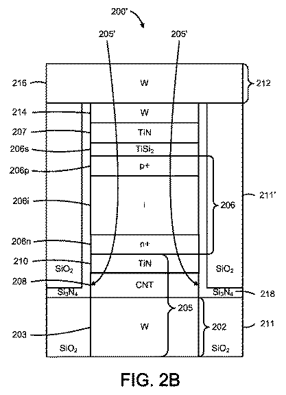
図2は、本発明に従って提供される代表的なメモリセル構造200の横断面立面図である。図2Aおよび2Bは、異なる順序で形成されるメモリセルの層を描いている。図2Aでは、メモリセル構造200は、誘電体側壁ライナと、底部電極および頂部電極の間に配置されているCNT膜とを有するMIMデバイスより下に配置されているダイオードを含む。図2Bでは、メモリセル構造200’は、MIMデバイスより上に配置されているダイオードを有する。
FIG. 2 is a cross-sectional elevation view of an exemplary
図2Aに示されているように、メモリセル構造200は、基板(図示せず)の上に形成された第1の導体202を含む。第1の導体202は、W、Cu、Al、Au、または他の金属層などの第1の金属層203と、第1の金属層203の上に形成されたTiN、TaNまたは類似層などの第1の障壁/接着層204とを含むことができる。図2Bに示されているように、第1の導体202はMIM層スタック構造205の下側部分を含んでMIM205の底部電極として機能することができる。一般的に、複数の第1の導体202が設けられて、例えば、パターニングされエッチングされ、例えば各々の第1の導体202の間にSiO2 または他の誘電体材料絶縁を使用することによって、互いから絶縁させることができる。
As shown in FIG. 2A, the
垂直pin(またはnip)ダイオード206が第1の導体202より上に形成される。例えば、ダイオード206は多結晶質(例えば、ポリシリコン、ポリゲルマニウム、シリコン−ゲルマニウム合金など)ダイオードを含むことができる。ダイオード206は、第1のタイプ(例えば、n形)のドーパントで強くドープされた半導体材料の層206nと、真性のあるいは軽くドープされた半導体材料の層206iと、第2のタイプ(例えば、p形)のドーパントで強くドープされた半導体材料の層206pとを含むことができる。あるいは、図2Bに示されているダイオード206と類似して、ダイオード206の層206n、206i、および206pの垂直方向順序は逆にされてもよい。
A vertical pin (or nip)
或る実施形態では、任意のシリサイド領域206sがダイオード206の上に形成され得る。あらゆる目的のためにその全体が本願明細書において参照により援用されている米国特許第7,176,064号(特許文献7)に記載されているように、チタンおよびコバルトなどのシリサイド形成材料が、アニーリング中、堆積したシリコンと反応してシリサイド層を形成する。チタンシリサイドおよびコバルトシリサイドの格子面間隔はシリコンのものに近くて、そのようなシリサイド層は、堆積したシリコンが結晶化するときに、隣接する堆積したシリコンのための「結晶化テンプレート」または「シード」として役立ち得ると思われる(例えば、シリサイド層は、アニーリング中、ダイオード206の結晶構造を強化する)。これにより、低抵抗率シリコンが提供される。シリコン−ゲルマニウム合金および/またはゲルマニウムのダイオードのために同様の結果が成し遂げられ得る。ダイオード206を結晶化させるためにシリサイド領域206sを用いる或る実施形態では、完成した構造にシリコン領域206sが残らないように、シリサイド領域206sは、そのような結晶化の後に除去され得る。
In certain embodiments, an optional silicide region 206 s can be formed over the
TiNまたは他の接着/障壁層または層スタック207がダイオード206より上に形成され得る。或る実施形態では、接着/障壁層207は、第1の接着/障壁層207aと、Wなどの金属層207bと、TiNなどのさらなる接着/障壁層207cとを含む層スタック207を含むことができる。
A TiN or other adhesion / barrier layer or
層スタック207が使用される場合には、層207aおよび207bは、化学的機械的平坦化(「CMP」)ストップ層および/またはエッチングストップ層として作用し得る金属ハードマスクとして役立つことができる。そのような手法は、例えば、あらゆる目的のためにその全体が本願明細書において参照により援用されている、2006年5月31日に出願された「CONDUCTIVE HARD MASK TO PROTECT PATTERNED FEATURES DURING TRENCH ETCH 」という米国特許出願第11/444,936号(特許文献8)に開示されている。例えば、ダイオード206と層207aおよび207bとを支柱を形成するためにパターニングしエッチングすることができ、それらの支柱の間に誘電体充填材料211が形成され得る。スタックは、その後、ギャップ充填材211および層207bを共同露出させるためにCMPまたはエッチバックなどによって平坦化され得る。その後、層207cが層207b上に形成され得る。あるいは、層207cは、ダイオード206と層207aおよび207bとともにパターニングされエッチングされ得る。或る実施形態では、層207cは除去されてもよく、CNT材料は金属層207b(例えば、W)と直に接続してもよい。
If
その後、(前に説明したように)任意の適切なCNT形成プロセスを用いてCNT材料208が接着/障壁層または層スタック207の上に形成され得る。CNT材料208の堆積/形成後、前に説明したように、任意の第2の炭素ベース材料層(図示せず)が、CNT材料208を覆う保護ライナとして形成され得る。CNT材料208の堆積/形成後、TiN、TaN、WN、Moなどの第2の接着/障壁層210がCNT材料208の上に形成される。
Thereafter, the
図2Aに示されているように、接着層207は、スイッチング層としてのCNT材料208と頂部電極としての接着層210とを含むMIM層スタック205の底部電極として機能することができる。それゆえ、次のセクションでは、図2Aに関して接着/障壁層207を「底部電極207」と称する。同様に、接着/障壁層210は、図2Aおよび図2BのMIM205の「頂部電極210」と称される。頂部電極210は、前に論じたように、低エネルギー堆積手法を用いて堆積させられ得る。(図に示されているように、)付加的なハードマスクおよび/またはCMPストップ層214も形成され得る。
As shown in FIG. 2A, the
接着層(図示せず)および伝導層216を含み得る頂部導体212の形成前に、図1に関して前に論じたように、層スタックはパターニングおよびエッチングされ得る。前に言及した支柱を作るためにエッチングプロセスが行われるとすれば、エッチングは層208、210に適用され、またことによると207cおよび214にも適用され得る。例えば、層214、210はCNT材料208のためのハードマスクおよび/またはCMPストップとして役立ち得る。
Prior to the formation of the
或る実施形態では、CNT材料208は、第2の接着/障壁層210のために使用されるエッチングステップとは異なるエッチングステップを用いてエッチングされ得る。他の実施形態では、単一のエッチングステップが使用され得る。そのようなエッチングされた膜スタックは、ほぼ垂直の側壁205’を有するとともにCNT材料208のアンダーカットをほとんどあるいは全く有しないということが観察されている。或る実施形態では、CNT材料208は、下にある誘電体ギャップ充填材料211のエッチングが生じ得るように、オーバーエッチングされ得る。
In some embodiments, the
頂部電極210およびCNT材料208のエッチング後、付加的な誘電体ギャップ充填材211’の堆積前に層スタックは洗浄され得る。洗浄後、ギャップ充填材211’の堆積前に、酸素に富むギャップ充填誘電体211’(例えば、SiO2 )の堆積の間のCNT材料208の側壁205’を保護するために貧酸素堆積化学的手法(例えば、高酸素プラズマ成分なし)で誘電体側壁ライナ218が形成され得る。誘電体側壁ライナ218は、誘電体前充填材ライナと称されてもよい。
After etching the
図2の実施形態では、標準的なPECVD SiO2 誘電体充填材211’が後に続く窒化シリコン誘電体側壁ライナ218が使用され得る。窒化シリコン誘電体側壁ライナ218は、化学式どおりおよび/または化学式どおりでない窒化シリコンを含むことができる。或る実施形態では、誘電体側壁ライナ218は約200〜約500オングストロームのSiNを含むことができる。しかし、この構造は、他の層の厚さおよび/または他の材料、例えばSix Cy Nz およびSix Oy Nz (低O含有量を有する)などを任意に含むことができ、ここでx、yおよびzは安定な化合物をもたらす非ゼロ数である。
In the embodiment of FIG. 2, a silicon nitride
誘電体側壁ライナ218は、例えば誘電体ギャップ充填材の残りなどのギャップ充填材部分211’が堆積させられる前に頂部電極/aC/CNT構造物の層スタックの上に共形に堆積させられる。誘電体側壁ライナ218は、好ましくはCNT材料208の外側壁205’を覆い、それらを誘電体充填材211’から絶縁させる。下にある誘電体ギャップ充填材料211のエッチングが生じるようにCNT材料208がオーバーエッチングされる実施形態では、誘電体側壁ライナ218はCNT材料108より下へ延びることができる。
A
頂部電極/CNT構造物の画定された層スタックは、SiO2または他の誘電体充填材211’で絶縁させられた後、頂部電極210、ギャップ充填材211’、およびSiN誘電体側壁ライナ218を共同露出させるために平坦化される。第2の接着/障壁層210の上に、あるいは、層214がハードマスクとして使用されて層208および210とともにエッチングされるならば層214の上に第2の導体212が形成される。第2の導体212は、図1および2に示されているように、TiN、TaN、WNまたは類似の層などの障壁/接着層と、Wまたは他の伝導層などの金属層216とを含むことができる。
After the defined layer stack of the top electrode / CNT structure is insulated with SiO 2 or other
図1とは対照的に、図2は、接着/障壁層210上に、スタックがエッチングされる前に堆積させられたタングステンの層214を描き、層214もエッチングされる。層214は、その下の層をエッチングするのに役立つ金属ハードマスクとして作用することができる。層214および216が両方ともタングステンであり得る限り、それらは互いによく接着するはずである。任意に、SiO2 ハードマスクが使用され得る。
1つの代表的な実施形態では、例えば前に援用されている特許文献6に記載されているように、SiN誘電体側壁ライナ218が形成され得る。
In contrast to FIG. 1, FIG. 2 depicts a
In one exemplary embodiment, a SiN
図2Bに示されているように、マイクロエレクトロニクス構造200’は、他の層の再配置を生じさせてCNT材料208より上に置かれたダイオード206を含むことができる。特に、CNT材料208は、図2Aに示されているように接着/障壁層204上に、あるいは図2Bに示されているように下側導体202上に直接堆積させられ得る。下側導体からのタングステンは、例えば、CNT材料208の形成を、それが成長させられるのであれば、触媒的に助けることができる。タングステンは、炭素によく付着するようにも思われる。接着/障壁層210を炭素ベースのスイッチング層208上に直接形成することができ、その後に、場合によってはシリサイド領域206sを含むことのあるダイオード206が形成される。接着/障壁層207がダイオード206上に(シリサイド領域206sを伴って、あるいは伴わずに)形成され得る。
As shown in FIG. 2B, the microelectronic structure 200 'can include a
図2Bは層207上にタングステンなどの層214を描き、この層214は、好ましくは同じくタングステンから作られる第2の導体212の金属層216に対して金属ハードマスクおよび/または接着層として役立つことができる。スタックは、前に説明したように、パターニングされエッチングされて支柱になることができる。或る実施形態では、層206、207、208、210、および214の層スタック全体が、単一のフォトリソグラフィステップを用いてパターニングされ得る。
FIG. 2B depicts a
図1に関して言及した任意の酸化物ハードマスクより上に、あるいはその代わりに、構造物サイズ、例えば限界寸法をさらに減少させるためにシリコンの層が形成されて可縮ハードマスクとして使用され得る。或る実施形態では、シリコンは、PECVD手法を用いて堆積させられたときに非晶質である。シリコンハードマスクを形成するためにPR層をパターニングしてパターンを非晶質シリコン内にエッチングした後、シリコンハードマスクはパターンの限界寸法を減少させるために収縮させられ得る。 A layer of silicon can be formed and used as a retractable hard mask above or instead of any oxide hard mask referred to with respect to FIG. 1 to further reduce structure size, eg, critical dimensions. In some embodiments, the silicon is amorphous when deposited using a PECVD technique. After patterning the PR layer and etching the pattern into amorphous silicon to form a silicon hard mask, the silicon hard mask can be contracted to reduce the critical dimension of the pattern.
誘電体側壁ライナ218は、柱と、第1の導体202を絶縁させる誘電体充填材211との上に共形に堆積させられ得る。この場合、誘電体側壁ライナ218は、第1の導体202と第2の導体212との間の層スタックの高さ全体に沿って上方に延びることができる。ギャップ充填材211’、金属ハードマスク層214、および誘電体側壁ライナ218を共同露出させるための平坦化の後に、図2Bに示されている構造200’を達成するために頂部導体212が形成される。
The
本発明の第3の代表的な実施形態に従って、マイクロエレクトロニクス構造の形成は、メモリセルを含むモノリシックな3次元メモリアレイの形成を含み、各メモリセルは、底部電極と頂部電極との間に配置されて誘電体側壁ライナにより覆われた炭素ベースの記憶素子を有するMIMデバイスを含む。炭素ベース記憶素子は、頂部電極が浸透しておらず、かつ好ましくは浸潤してもいない、無損傷あるいは低損傷のCNT材料を覆う任意の炭素ベース保護層を含むことができる。MIM内の頂部電極は、任意に、低エネルギー堆積手法を用いて堆積させられ得る。 According to a third exemplary embodiment of the present invention, the formation of a microelectronic structure includes the formation of a monolithic three-dimensional memory array that includes memory cells, each memory cell being disposed between a bottom electrode and a top electrode. A MIM device having a carbon-based storage element covered by a dielectric sidewall liner. The carbon-based storage element can include an optional carbon-based protective layer covering undamaged or low-damaged CNT material that is not penetrated and preferably not infiltrated by the top electrode. The top electrode in the MIM can optionally be deposited using a low energy deposition technique.
図3は、本発明の第3の代表的な実施形態に従って形成された代表的なメモリセルのメモリアレイ300の一部分を示す。第1のメモリレベルは基板より上に形成され、それより上に追加のメモリレベルが形成され得る。メモリアレイ形成に関する詳しいことは、本願明細書において参照により援用されている特許文献に記載され、そのようなアレイは、本発明の実施形態に従う方法および構造を使用することから利益を得ることができる。
FIG. 3 illustrates a portion of a
図3に示されているように、メモリアレイ300は、ワード線またはビット線としてそれぞれ役立ち得る第1の導体310および310’と、支柱320および320’(各支柱320、320’はメモリセルを含む)と、ビット線またはワード線としてそれぞれ役立ち得る第2の導体330とを含むことができる。第1の導体310、310’は、第2の導体330に対して実質的に垂直に描かれている。メモリアレイ300は、1つ以上のメモリレベルを含むことができる。第1のメモリレベル340は第1の導体310、支柱320および第2の導体330の組み合わせを含むことができ、第2のメモリレベル350は第2の導体330、支柱320’および第1の導体310’を含むことができる。このようなメモリレベルの製造は、本願明細書において参照により援用されている特許文献に詳しく記載されている。
As shown in FIG. 3, the
本発明の実施形態は、モノリシックな3次元メモリアレイを形成するために有用である。モノリシックな3次元メモリアレイは、複数のメモリレベルがウェハなどの単一の基板より上に、介在する基板なしで、形成されるものである。1つのメモリレベルを形成する層は、既存の1つまたは複数のレベルの層の上に直接堆積あるいは成長させられる。対照的に、積層されたメモリは、Leedy の米国特許第5,915,167号(特許文献9)のように、複数のメモリレベルを別々の基板上に形成してそれらのメモリレベルを互いの上に接着させることによって構築されている。それらの基板は接着の前に薄くされるかあるいはメモリレベルから除去されるけれども、メモリレベルは初めに別々の基板の上に形成されるので、そのようなメモリは真のモノリシックな3次元メモリアレイではない。 Embodiments of the present invention are useful for forming monolithic three-dimensional memory arrays. A monolithic three-dimensional memory array is one in which multiple memory levels are formed above a single substrate, such as a wafer, without an intervening substrate. The layers that form a memory level are deposited or grown directly on the existing one or more levels. In contrast, stacked memories, such as Leedy U.S. Pat. No. 5,915,167, form multiple memory levels on separate substrates and set the memory levels to each other. Built by gluing on top. Although those substrates are thinned or removed from the memory level prior to bonding, such a memory is a true monolithic three-dimensional memory array because the memory levels are initially formed on separate substrates. is not.
関連するメモリが、2004年9月29日に出願されたHernerらの「NONVOLATILE MEMORY CELL WITHOUT A DIELECTRIC ANTIFUSE HAVING HIGH- AND LOW-IMPEDANCE STATES」という米国特許出願第10/955,549号(特許文献10)に記載され、あらゆる目的のためにその全体が本願明細書において参照により援用されている。特許文献10は、図2のダイオード206のような垂直に向けられたpinダイオードを含むモノリシックな3次元メモリアレイを記述している。形成されたとき、特許文献10のpinダイオードのポリシリコンは高抵抗状態にある。プログラミング電圧を印加すると、ポリシリコンの性質は恒久的に変化して低抵抗となる。あらゆる目的のためにその全体が本願明細書において参照により援用されている、2005年6月8日に出願されたHernerらの「NONVOLATILE MEMORY CELL OPERATING BY INCREASING ORDER IN POLYCRYSTALLINE SEMICONDUCTOR MATERIAL 」という米国特許出願第11/148,530号(特許文献11)により充分に記載されているように、変化はポリシリコンにおける結晶配列の程度の高まりによって引き起こされると考えられる。
The related memory is US Patent Application No. 10 / 955,549 entitled “NONVOLATILE MEMORY CELL WITHOUT A DIELECTRIC ANTIFUSE HAVING HIGH- AND LOW-IMPEDANCE STATES” filed on September 29, 2004. And are incorporated herein by reference in their entirety for all purposes. U.S. Patent No. 6,057,031 describes a monolithic three-dimensional memory array that includes vertically oriented pin diodes, such as
他の1つの関連するメモリがHernerらの米国特許第7,285,464号(特許文献12)に記載され、その全体が本願明細書において参照により援用されている。特許文献12に記載されているように、pinダイオードの高さを小さくすると有利である。ダイオードが短ければ、必要なプログラミング電圧は低く、隣接するダイオード間のギャップのアスペクト比は小さくなる。非常にアスペクト比の高いギャップを隙間(欠損)がないように充填するのは困難である。逆バイアス時のダイオードの電流リークを減少させるために真性領域については少なくとも600オングストロームの厚さが好ましい。強くn形ドープされた層より上に貧シリコン真性層があって、その両者がシリコン−ゲルマニウムの薄い真性キャッピング層で分離されているダイオードを形成すれば、ドーパントのプロファイルのより鋭い遷移が考慮され、従ってダイオードの全高が小さくされることになる。 Another related memory is described in US Pat. No. 7,285,464 to Herner et al., Which is hereby incorporated by reference in its entirety. As described in Patent Document 12, it is advantageous to reduce the height of the pin diode. The shorter the diode, the lower the programming voltage required and the smaller the aspect ratio of the gap between adjacent diodes. It is difficult to fill a gap having a very high aspect ratio so that there is no gap (defect). A thickness of at least 600 Angstroms is preferred for the intrinsic region to reduce diode current leakage during reverse bias. Forming a diode with a poor silicon intrinsic layer above a strongly n-doped layer, both separated by a thin intrinsic capping layer of silicon-germanium, allows for sharper transitions in the dopant profile. Therefore, the total height of the diode is reduced.
特に、類似するメモリレベルの製造に関する詳細な情報が、前に援用されている特許文献10および特許文献12で提供されている。関連するメモリの製造に関するより多くの情報が、本発明の譲受人により所有され、あらゆる目的のためにその全体が本願明細書において参照により援用されている、Hernerらの「A HIGH-DENSITY THREE-DIMENSIONAL MEMORY CELL」という米国特許第6,952,030号(特許文献13)で提供されている。本発明を不明瞭にしないために、この詳細は本願明細書において繰り返して述べられないけれども、これらあるいは他の援用されている特許または特許出願のどの教示も除外されるべく意図されてはいない。前の例が非限定的であることおよび本願明細書において提供されている詳細は、結果が本発明の範囲内に属するような改変、省略あるいは拡張がなされ得るということが理解されるはずである。 In particular, detailed information regarding the manufacture of similar memory levels is provided in US Pat. More information regarding the manufacture of related memories is owned by the assignee of the present invention and incorporated by reference herein in its entirety for all purposes, Herner et al., “A HIGH-DENSITY THREE- DIMENSIONAL MEMORY CELL "is provided in US Pat. No. 6,952,030 (Patent Document 13). In order not to obscure the present invention, this detail is not repeated herein, but is not intended to exclude any teaching of these or other incorporated patents or patent applications. It should be understood that the previous examples are non-limiting and the details provided herein can be modified, omitted or expanded such that the results are within the scope of the invention. .
前の記述は本発明の代表的な実施形態を開示している。前に開示された装置および方法の、本発明の範囲に属する改変は、当業者にとってすべて明らかになるはずである。従って、本発明は代表的な実施形態と関連して開示されたけれども、添付の特許請求の範囲により定義される発明の趣旨および範囲に他の実施形態が属し得るということが理解されるべきである。 The previous description discloses exemplary embodiments of the invention. All modifications of the previously disclosed apparatus and methods that fall within the scope of the present invention should be apparent to those skilled in the art. Thus, although the invention has been disclosed in connection with exemplary embodiments, it is to be understood that other embodiments can fall within the spirit and scope of the invention as defined by the appended claims. is there.
Claims (38)
前記基板をマスキング層でコーティングするステップと、
前記マスキング層をパターニングするステップと、
前記パターニングされたマスキング層を通して非酸素ベースの化学的手法を用いて前記CNT膜をエッチングするステップと、
を含む方法。 A method of etching a carbon nanotube (“CNT”) film formed on a substrate, comprising:
Coating the substrate with a masking layer;
Patterning the masking layer;
Etching the CNT film using a non-oxygen based chemical technique through the patterned masking layer;
Including methods.
前記CNT膜をエッチングするステップは、
前記基板をプラズマエッチングチャンバの中に装填するステップと、
三塩化ホウ素(「BCl3 」)およびジクロリン(「Cl2 」)を用いて前記基板をエッチングするステップと、
を含む方法。 The method of claim 1, wherein
Etching the CNT film comprises:
Loading the substrate into a plasma etch chamber;
Etching the substrate with boron trichloride (“BCl 3 ”) and dichlorin (“Cl 2 ”);
Including methods.
前記基板をエッチングするステップは、約70:1から約3:5までのBCl3 対Cl2 比を用いることを含む方法。 The method of claim 2, wherein
Etching the substrate includes using a BCl 3 to Cl 2 ratio of about 70: 1 to about 3: 5.
前記基板をエッチングするステップは、約4:1から約1.8:1までのBCl3 対Cl2 比を用いることを含む方法。 The method of claim 2, wherein
Etching the substrate includes using a BCl 3 to Cl 2 ratio of about 4: 1 to about 1.8: 1.
前記基板をエッチングするステップは、約5:2のBCl3 対Cl2 比を用いることを含む方法。 The method of claim 2, wherein
Etching the substrate includes using a BCl 3 to Cl 2 ratio of about 5: 2.
前記基板をエッチングするステップは、アルゴン(「Ar」)を用いることをさらに含む方法。 The method of claim 2, wherein
Etching the substrate further comprises using argon (“Ar”).
前記基板をエッチングするステップは、約70:1:1から約3:5:5までのBCl3 対Cl2 対Ar比を用いることを含む方法。 The method of claim 6 wherein:
Etching the substrate includes using a BCl 3 to Cl 2 to Ar ratio of about 70: 1: 1 to about 3: 5: 5.
前記基板をエッチングするステップは、約4:1:1から約1.8:1:1までのBCl3 対Cl2 対Ar比を用いることを含む方法。 The method of claim 6 wherein:
Etching the substrate includes using a BCl 3 to Cl 2 to Ar ratio of about 4: 1: 1 to about 1.8: 1: 1.
前記基板をエッチングするステップは、約5:2:2のBCl3 対Cl2 対Ar比を用いることを含む方法。 The method of claim 6 wherein:
Etching the substrate includes using a BCl 3 to Cl 2 to Ar ratio of about 5: 2: 2.
前記マスキング層は、フォトレジストを含む方法。 The method of claim 1, wherein
The masking layer includes a photoresist.
前記フォトレジストを灰化するステップをさらに含む方法。 The method of claim 10, wherein:
The method further comprising ashing the photoresist.
前記フォトレジストは、前記基板をエッチングする前に灰化される方法。 The method of claim 11 wherein:
The method wherein the photoresist is ashed prior to etching the substrate.
前記フォトレジストは、前記基板をエッチングした後に灰化される方法。 The method of claim 11 wherein:
The photoresist is ashed after etching the substrate.
前記灰化するステップは、2ステップ灰化手続きを含む方法。 The method of claim 11 wherein:
The ashing step includes a two-step ashing procedure.
基板より上にカーボンナノチューブ(「CNT」)材料の層を形成するステップと、
三塩化ホウ素(「BCl3 」)およびジクロリン(「Cl2 」)ならびに約50および約150ワットの間の基板バイアス電力を用いて前記CNT材料をプラズマエッチングチャンバ内でエッチングするステップと、
を含む方法。 A method of forming a memory cell, comprising:
Forming a layer of carbon nanotube ("CNT") material above the substrate;
Etching the CNT material in a plasma etch chamber using boron trichloride (“BCl 3 ”) and dichlorin (“Cl 2 ”) and a substrate bias power between about 50 and about 150 Watts;
Including methods.
前記基板バイアス電力は、約85および約110ワットの間にある方法。 The method of claim 16, wherein
The method wherein the substrate bias power is between about 85 and about 110 watts.
前記基板バイアス電力は、約100ワットである方法。 The method of claim 16, wherein
The method wherein the substrate bias power is about 100 watts.
前記CNT材料をエッチングするステップは、約70:1から約3:5までのBCl3 対Cl2 比を用いることを含む方法。 The method of claim 16, wherein
Etching the CNT material comprises using a BCl 3 to Cl 2 ratio of about 70: 1 to about 3: 5.
前記CNT材料をエッチングするステップは、約4:1から約1.8:1までのBCl3 対Cl2 比を用いることを含む方法。 The method of claim 16, wherein
Etching the CNT material comprises using a BCl 3 to Cl 2 ratio of about 4: 1 to about 1.8: 1.
前記CNT材料をエッチングするステップは、約5:2のBCl3 対Cl2 比を用いることを含む方法。 The method of claim 16, wherein
Etching the CNT material comprises using a BCl 3 to Cl 2 ratio of about 5: 2.
前記CNT材料をエッチングするステップは、アルゴン(「Ar」)を用いることをさらに含む方法。 The method of claim 17, wherein
Etching the CNT material further comprises using argon (“Ar”).
前記CNT材料をエッチングするステップは、約70:1:1から約3:5:5までのBCl3 対Cl2 対Ar比を用いることを含む方法。 The method of claim 22, wherein
Etching the CNT material comprises using a BCl 3 to Cl 2 to Ar ratio of about 70: 1: 1 to about 3: 5: 5.
前記CNT材料をエッチングするステップは、約4:1:1から約1.8:1:1までのBCl3 対Cl2 対Ar比を用いることを含む方法。 The method of claim 22, wherein
Etching the CNT material comprises using a BCl 3 to Cl 2 to Ar ratio of about 4: 1: 1 to about 1.8: 1: 1.
前記CNT材料をエッチングするステップは、約5:2:2のBCl3 対Cl2 対Ar比を用いることを含む方法。 The method of claim 22, wherein
Etching the CNT material includes using a BCl 3 to Cl 2 to Ar ratio of about 5: 2: 2.
前記CNT層に結合されるステアリング素子を形成するステップをさらに含む方法。 The method of claim 17, wherein
Forming a steering element coupled to the CNT layer;
前記ステアリング素子は、ダイオードを含む方法。 The method of claim 26.
The method wherein the steering element comprises a diode.
前記ステアリング素子を形成するステップは、
前記基板より上にシリコンの1つ以上の層を形成するステップと、
前記シリコンの1つ以上の層をエッチングするステップと、
を含む方法。 28. The method of claim 27, wherein
Forming the steering element comprises:
Forming one or more layers of silicon above the substrate;
Etching one or more layers of the silicon;
Including methods.
前記シリコンの1つ以上の層と前記CNT層とを単一のエッチングステップでエッチングするステップを含む方法。 30. The method of claim 28, wherein
Etching the one or more layers of silicon and the CNT layer in a single etching step.
前記シリコンの1つ以上の層と前記CNT層とを別々にエッチングするステップを含む方法。 30. The method of claim 28, wherein
Etching the one or more layers of silicon and the CNT layer separately.
基板より上にカーボンナノチューブ(「CNT」)材料の層を形成するステップと、
ほとんど垂直の側壁を有するとともに前記CNT材料のアンダーカットをほとんどあるいは全く有しないように前記CNT材料をエッチングするために非酸素ベースの化学的手法を用いるステップと、
を含む方法。 A method of forming a memory cell, comprising:
Forming a layer of carbon nanotube ("CNT") material above the substrate;
Using a non-oxygen-based chemical technique to etch the CNT material so as to have almost vertical sidewalls and little or no undercutting of the CNT material;
Including methods.
前記CNT層に結合されるステアリング素子を形成するステップをさらに含む方法。 The method of claim 32, wherein
Forming a steering element coupled to the CNT layer;
前記ステアリング素子は、ダイオードを含む方法。 34. The method of claim 33.
The method wherein the steering element comprises a diode.
前記ステアリング素子を形成するステップは、
前記基板より上にシリコンの1つ以上の層を形成するステップと、
前記シリコンの1つ以上の層をエッチングするステップと、
を含む方法。 35. The method of claim 34.
Forming the steering element comprises:
Forming one or more layers of silicon above the substrate;
Etching one or more layers of the silicon;
Including methods.
前記シリコンの1つ以上の層と前記CNT層とを単一のエッチングステップでエッチングするステップを含む方法。 36. The method of claim 35, wherein
Etching the one or more layers of silicon and the CNT layer in a single etching step.
前記シリコンの1つ以上の層と前記CNT層とを別々にエッチングするステップを含む方法。 36. The method of claim 35, wherein
Etching the one or more layers of silicon and the CNT layer separately.
Applications Claiming Priority (5)
| Application Number | Priority Date | Filing Date | Title |
|---|---|---|---|
| US4431408P | 2008-04-11 | 2008-04-11 | |
| US61/044,314 | 2008-04-11 | ||
| US8102908P | 2008-07-15 | 2008-07-15 | |
| US61/081,029 | 2008-07-15 | ||
| PCT/US2009/040215 WO2009126891A1 (en) | 2008-04-11 | 2009-04-10 | Methods for etching carbon nano-tube films for use in non-volatile memories |
Publications (1)
| Publication Number | Publication Date |
|---|---|
| JP2011520249A true JP2011520249A (en) | 2011-07-14 |
Family
ID=40749194
Family Applications (1)
| Application Number | Title | Priority Date | Filing Date |
|---|---|---|---|
| JP2011504204A Pending JP2011520249A (en) | 2008-04-11 | 2009-04-10 | Method for etching carbon nanotube film used in non-volatile memory |
Country Status (7)
| Country | Link |
|---|---|
| US (1) | US8445385B2 (en) |
| EP (1) | EP2263252B1 (en) |
| JP (1) | JP2011520249A (en) |
| KR (1) | KR20100136490A (en) |
| CN (1) | CN102067292B (en) |
| TW (1) | TW201007836A (en) |
| WO (1) | WO2009126891A1 (en) |
Cited By (5)
| Publication number | Priority date | Publication date | Assignee | Title |
|---|---|---|---|---|
| JP2011129705A (en) * | 2009-12-17 | 2011-06-30 | Toshiba Corp | Semiconductor memory device |
| US9111611B2 (en) | 2013-09-05 | 2015-08-18 | Kabushiki Kaisha Toshiba | Memory system |
| KR20170038000A (en) * | 2014-09-26 | 2017-04-05 | 인텔 코포레이션 | Laminate diffusion barriers and related devices and methods |
| KR101770456B1 (en) * | 2014-03-04 | 2017-09-05 | 타이완 세미콘덕터 매뉴팩쳐링 컴퍼니 리미티드 | Rram cell structure with conductive etch-stop layer |
| JP6999120B1 (en) | 2021-03-19 | 2022-02-14 | 国立大学法人信州大学 | Manufacturing method of rectifying element |
Families Citing this family (23)
| Publication number | Priority date | Publication date | Assignee | Title |
|---|---|---|---|---|
| JP2007212006A (en) * | 2006-02-07 | 2007-08-23 | Nissan Motor Co Ltd | Combustion state detection device for catalytic combustor |
| US8133793B2 (en) | 2008-05-16 | 2012-03-13 | Sandisk 3D Llc | Carbon nano-film reversible resistance-switchable elements and methods of forming the same |
| US8569730B2 (en) * | 2008-07-08 | 2013-10-29 | Sandisk 3D Llc | Carbon-based interface layer for a memory device and methods of forming the same |
| US8466044B2 (en) * | 2008-08-07 | 2013-06-18 | Sandisk 3D Llc | Memory cell that includes a carbon-based memory element and methods forming the same |
| US7687308B2 (en) * | 2008-08-15 | 2010-03-30 | Texas Instruments Incorporated | Method for fabricating carbon nanotube transistors on a silicon or SOI substrate |
| WO2010022097A1 (en) * | 2008-08-19 | 2010-02-25 | Sandisk 3D, Llc | Methods for increasing carbon nano-tube (cnt) yield in memory devices |
| US20100108976A1 (en) * | 2008-10-30 | 2010-05-06 | Sandisk 3D Llc | Electronic devices including carbon-based films, and methods of forming such devices |
| US8835892B2 (en) * | 2008-10-30 | 2014-09-16 | Sandisk 3D Llc | Electronic devices including carbon nano-tube films having boron nitride-based liners, and methods of forming the same |
| US8421050B2 (en) * | 2008-10-30 | 2013-04-16 | Sandisk 3D Llc | Electronic devices including carbon nano-tube films having carbon-based liners, and methods of forming the same |
| US8481396B2 (en) * | 2009-10-23 | 2013-07-09 | Sandisk 3D Llc | Memory cell that includes a carbon-based reversible resistance switching element compatible with a steering element, and methods of forming the same |
| US8389375B2 (en) * | 2010-02-11 | 2013-03-05 | Sandisk 3D Llc | Memory cell formed using a recess and methods for forming the same |
| US8237146B2 (en) | 2010-02-24 | 2012-08-07 | Sandisk 3D Llc | Memory cell with silicon-containing carbon switching layer and methods for forming the same |
| US8481394B2 (en) * | 2010-03-04 | 2013-07-09 | Sandisk 3D Llc | Memory cell that includes a carbon-based memory element and methods of forming the same |
| CN102893421B (en) | 2010-05-21 | 2016-01-20 | 默克专利股份有限公司 | At the selective etch of the structural carbon nano-tube of plastic bottom material (CNT) polymer substrate |
| JP5572056B2 (en) | 2010-10-20 | 2014-08-13 | 株式会社東芝 | Storage device and manufacturing method thereof |
| US20120223414A1 (en) * | 2011-03-02 | 2012-09-06 | Schricker April D | Methods for increasing bottom electrode performance in carbon-based memory devices |
| US9753001B1 (en) * | 2011-09-23 | 2017-09-05 | The United States Of America As Represented By The Administrator Of National Aeronautics And Space Administration | Polymer nanofiber based reversible nano-switch/sensor diode (nanoSSSD) device |
| US10084016B2 (en) | 2013-11-21 | 2018-09-25 | Micron Technology, Inc. | Cross-point memory and methods for fabrication of same |
| US9385316B2 (en) | 2014-01-07 | 2016-07-05 | Taiwan Semiconductor Manufacturing Co., Ltd. | RRAM retention by depositing Ti capping layer before HK HfO |
| JP6317694B2 (en) * | 2015-03-16 | 2018-04-25 | 株式会社東芝 | Semiconductor device |
| US9923139B2 (en) * | 2016-03-11 | 2018-03-20 | Micron Technology, Inc. | Conductive hard mask for memory device formation |
| US10892406B2 (en) | 2018-06-04 | 2021-01-12 | Intel Corporation | Phase change memory structures and devices |
| CN111293072B (en) * | 2018-12-10 | 2023-06-20 | 联华电子股份有限公司 | Semiconductor element and manufacturing method thereof |
Family Cites Families (22)
| Publication number | Priority date | Publication date | Assignee | Title |
|---|---|---|---|---|
| US5915167A (en) | 1997-04-04 | 1999-06-22 | Elm Technology Corporation | Three dimensional structure memory |
| US6034882A (en) | 1998-11-16 | 2000-03-07 | Matrix Semiconductor, Inc. | Vertically stacked field programmable nonvolatile memory and method of fabrication |
| US6706402B2 (en) | 2001-07-25 | 2004-03-16 | Nantero, Inc. | Nanotube films and articles |
| JP2003092287A (en) * | 2001-09-19 | 2003-03-28 | Nec Corp | Ashing method |
| US7405854B2 (en) * | 2002-03-21 | 2008-07-29 | Cornell Research Foundation, Inc. | Fibrous micro-composite material |
| CN1252817C (en) * | 2002-06-05 | 2006-04-19 | 中国科学院物理研究所 | Single electron memory having carbon nano tube structure and process for making it |
| AU2003258969A1 (en) * | 2002-06-27 | 2004-01-19 | Nanosys Inc. | Planar nanowire based sensor elements, devices, systems and methods for using and making same |
| US7176064B2 (en) | 2003-12-03 | 2007-02-13 | Sandisk 3D Llc | Memory cell comprising a semiconductor junction diode crystallized adjacent to a silicide |
| US8637366B2 (en) | 2002-12-19 | 2014-01-28 | Sandisk 3D Llc | Nonvolatile memory cell without a dielectric antifuse having high- and low-impedance states |
| WO2004061851A2 (en) | 2002-12-19 | 2004-07-22 | Matrix Semiconductor, Inc | An improved method for making high-density nonvolatile memory |
| US7285464B2 (en) | 2002-12-19 | 2007-10-23 | Sandisk 3D Llc | Nonvolatile memory cell comprising a reduced height vertical diode |
| US20050226067A1 (en) | 2002-12-19 | 2005-10-13 | Matrix Semiconductor, Inc. | Nonvolatile memory cell operating by increasing order in polycrystalline semiconductor material |
| KR100533316B1 (en) * | 2004-03-27 | 2005-12-02 | 한국과학기술원 | Method for Manufacturing a Carbon Nanotube Multilayer Pattern Using Photolithography and Dry Etching |
| US20060220094A1 (en) * | 2005-03-31 | 2006-10-05 | Bohumil Lojek | Non-volatile memory transistor with nanotube floating gate |
| US9196615B2 (en) * | 2005-05-09 | 2015-11-24 | Nantero Inc. | Nonvolatile nanotube diodes and nonvolatile nanotube blocks and systems using same and methods of making same |
| US7538040B2 (en) * | 2005-06-30 | 2009-05-26 | Nantero, Inc. | Techniques for precision pattern transfer of carbon nanotubes from photo mask to wafers |
| US8896045B2 (en) * | 2006-04-19 | 2014-11-25 | Infineon Technologies Ag | Integrated circuit including sidewall spacer |
| US7575984B2 (en) | 2006-05-31 | 2009-08-18 | Sandisk 3D Llc | Conductive hard mask to protect patterned features during trench etch |
| KR101486406B1 (en) * | 2006-08-08 | 2015-01-26 | 난테로 인크. | Nonvolatile Resistor Memory with Scalable Two-Terminal Nanotube Switch, Latch Circuit and Computing Circuit |
| US8236623B2 (en) * | 2007-12-31 | 2012-08-07 | Sandisk 3D Llc | Memory cell that employs a selectively fabricated carbon nano-tube reversible resistance-switching element and methods of forming the same |
| US8558220B2 (en) * | 2007-12-31 | 2013-10-15 | Sandisk 3D Llc | Memory cell that employs a selectively fabricated carbon nano-tube reversible resistance-switching element formed over a bottom conductor and methods of forming the same |
| US20090166610A1 (en) | 2007-12-31 | 2009-07-02 | April Schricker | Memory cell with planarized carbon nanotube layer and methods of forming the same |
-
2009
- 2009-04-10 US US12/421,803 patent/US8445385B2/en not_active Expired - Fee Related
- 2009-04-10 CN CN2009801223080A patent/CN102067292B/en active Active
- 2009-04-10 KR KR1020107022552A patent/KR20100136490A/en not_active Withdrawn
- 2009-04-10 TW TW098112126A patent/TW201007836A/en unknown
- 2009-04-10 WO PCT/US2009/040215 patent/WO2009126891A1/en not_active Ceased
- 2009-04-10 JP JP2011504204A patent/JP2011520249A/en active Pending
- 2009-04-10 EP EP09730879.5A patent/EP2263252B1/en not_active Not-in-force
Cited By (9)
| Publication number | Priority date | Publication date | Assignee | Title |
|---|---|---|---|---|
| JP2011129705A (en) * | 2009-12-17 | 2011-06-30 | Toshiba Corp | Semiconductor memory device |
| US9111611B2 (en) | 2013-09-05 | 2015-08-18 | Kabushiki Kaisha Toshiba | Memory system |
| KR101770456B1 (en) * | 2014-03-04 | 2017-09-05 | 타이완 세미콘덕터 매뉴팩쳐링 컴퍼니 리미티드 | Rram cell structure with conductive etch-stop layer |
| KR20170038000A (en) * | 2014-09-26 | 2017-04-05 | 인텔 코포레이션 | Laminate diffusion barriers and related devices and methods |
| JP2017532771A (en) * | 2014-09-26 | 2017-11-02 | インテル・コーポレーション | Laminated diffusion barrier and related devices and methods |
| US11133461B2 (en) | 2014-09-26 | 2021-09-28 | Intel Corporation | Laminate diffusion barriers and related devices and methods |
| KR102314670B1 (en) * | 2014-09-26 | 2021-10-20 | 인텔 코포레이션 | Laminate diffusion barriers and related devices and methods |
| JP6999120B1 (en) | 2021-03-19 | 2022-02-14 | 国立大学法人信州大学 | Manufacturing method of rectifying element |
| JP2022144856A (en) * | 2021-03-19 | 2022-10-03 | 国立大学法人信州大学 | Manufacturing method of rectifying element |
Also Published As
| Publication number | Publication date |
|---|---|
| TW201007836A (en) | 2010-02-16 |
| WO2009126891A1 (en) | 2009-10-15 |
| CN102067292B (en) | 2013-08-14 |
| KR20100136490A (en) | 2010-12-28 |
| US20090278112A1 (en) | 2009-11-12 |
| EP2263252A1 (en) | 2010-12-22 |
| EP2263252B1 (en) | 2013-10-09 |
| US8445385B2 (en) | 2013-05-21 |
| CN102067292A (en) | 2011-05-18 |
Similar Documents
| Publication | Publication Date | Title |
|---|---|---|
| JP2011520249A (en) | Method for etching carbon nanotube film used in non-volatile memory | |
| US8421050B2 (en) | Electronic devices including carbon nano-tube films having carbon-based liners, and methods of forming the same | |
| US8467224B2 (en) | Damascene integration methods for graphitic films in three-dimensional memories and memories formed therefrom | |
| US8309407B2 (en) | Electronic devices including carbon-based films having sidewall liners, and methods of forming such devices | |
| US8835892B2 (en) | Electronic devices including carbon nano-tube films having boron nitride-based liners, and methods of forming the same | |
| US20100108976A1 (en) | Electronic devices including carbon-based films, and methods of forming such devices | |
| US9047949B2 (en) | Non-volatile storage system using opposite polarity programming signals for MIM memory cell | |
| JP5564035B2 (en) | Memory cell including carbon-based memory device and method of forming the same | |
| US8023310B2 (en) | Nonvolatile memory cell including carbon storage element formed on a silicide layer | |
| US8309415B2 (en) | Methods and apparatus for increasing memory density using diode layer sharing | |
| JP2012507150A (en) | Carbon-based memory device exhibiting reduced delamination characteristics and method for forming the same | |
| TW201017759A (en) | A memory cell that includes a carbon-based memory element and methods of forming the same | |
| KR20120132625A (en) | Memory cell formed using a recess and methods for forming the same | |
| KR20130056205A (en) | Memory cell with silicon-containing carbon switching layer and methods for forming the same | |
| JP2012533885A (en) | How to make damascene diodes using sacrificial materials | |
| JP2011517122A (en) | Memory cell using carbon nanotube reversible resistance switching element formed selectively on lower conductor and method of forming the same | |
| US8093123B2 (en) | Integration methods for carbon films in two- and three-dimensional memories formed therefrom | |
| US8481394B2 (en) | Memory cell that includes a carbon-based memory element and methods of forming the same |