JP2011507471A - Adjustable low voltage charge pump - Google Patents
Adjustable low voltage charge pump Download PDFInfo
- Publication number
- JP2011507471A JP2011507471A JP2010538076A JP2010538076A JP2011507471A JP 2011507471 A JP2011507471 A JP 2011507471A JP 2010538076 A JP2010538076 A JP 2010538076A JP 2010538076 A JP2010538076 A JP 2010538076A JP 2011507471 A JP2011507471 A JP 2011507471A
- Authority
- JP
- Japan
- Prior art keywords
- capacitor
- charge pump
- voltage
- plate
- series
- Prior art date
- Legal status (The legal status is an assumption and is not a legal conclusion. Google has not performed a legal analysis and makes no representation as to the accuracy of the status listed.)
- Pending
Links
Images


Classifications
-
- H—ELECTRICITY
- H02—GENERATION; CONVERSION OR DISTRIBUTION OF ELECTRIC POWER
- H02M—APPARATUS FOR CONVERSION BETWEEN AC AND AC, BETWEEN AC AND DC, OR BETWEEN DC AND DC, AND FOR USE WITH MAINS OR SIMILAR POWER SUPPLY SYSTEMS; CONVERSION OF DC OR AC INPUT POWER INTO SURGE OUTPUT POWER; CONTROL OR REGULATION THEREOF
- H02M3/00—Conversion of dc power input into dc power output
- H02M3/02—Conversion of dc power input into dc power output without intermediate conversion into ac
- H02M3/04—Conversion of dc power input into dc power output without intermediate conversion into ac by static converters
- H02M3/06—Conversion of dc power input into dc power output without intermediate conversion into ac by static converters using resistors or capacitors, e.g. potential divider
- H02M3/07—Conversion of dc power input into dc power output without intermediate conversion into ac by static converters using resistors or capacitors, e.g. potential divider using capacitors charged and discharged alternately by semiconductor devices with control electrode, e.g. charge pumps
Abstract
低出力電圧、高電流能力のチャージポンプを提供する技術を説明する。このチャージポンプは切替回路と複数のコンデンサを有する。初期化段階には各コンデンサの第1の極板がレギュレータ電圧を受け取るように接続され、各コンデンサの第2の極板は接地へ接続される。移動段階にはコンデンサが直列に接続され、第1のコンデンサより後ろの各コンデンサでは第2の極板が直列内の先行コンデンサの第1の極板へ接続される。ポンプの出力電圧は、直列内の最終コンデンサの第1の極板から供給される。ポンプの出力電圧レベルに応じた値を得るため、調整回路は基準電圧からレギュレータ電圧を生成する。 A technique for providing a charge pump with low output voltage and high current capability will be described. This charge pump has a switching circuit and a plurality of capacitors. During the initialization phase, the first plate of each capacitor is connected to receive the regulator voltage, and the second plate of each capacitor is connected to ground. In the moving stage, capacitors are connected in series, and in each capacitor behind the first capacitor, the second plate is connected to the first plate of the preceding capacitor in the series. The pump output voltage is supplied from the first plate of the last capacitor in series. In order to obtain a value corresponding to the output voltage level of the pump, the adjustment circuit generates a regulator voltage from the reference voltage.
Description
本発明は、一般的にはチャージポンプの分野に関し、より具体的には相対的に低出力電圧、高電力効率、および高電流が要求されるチャージポンプに関する。 The present invention relates generally to the field of charge pumps, and more specifically to charge pumps that require relatively low output voltage, high power efficiency, and high current.
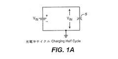
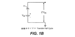
チャージポンプは切替処理によりDC入力電圧より大きいDC出力電圧を提供する。チャージポンプは通常、入力と出力との間にスイッチに結合されたコンデンサを有する。1クロックの半サイクルにあたる充電半サイクルのときには、コンデンサが入力へ並列に結合し、入力電圧まで充電する。第2のクロックサイクルにあたる移動半サイクルのときには、充電されたコンデンサが入力電圧と直列に結合し、入力電圧レベルの2倍の出力電圧を提供する。このプロセスは図1aおよび図1bに示されている。充電半サイクルを示す図1aではコンデンサ5が、入力電圧VINと並列に配置されている。移動半サイクルを示す図1bでは、充電されたコンデンサ5が入力電圧と直列に配置されている。図1bに見られるように、充電されたコンデンサ5の正端子は接地に対して2*VINになる。
The charge pump provides a DC output voltage greater than the DC input voltage by a switching process. A charge pump typically has a capacitor coupled to a switch between the input and the output. During the charging half cycle, which is one clock half cycle, a capacitor is coupled in parallel to the input and charged to the input voltage. During the moving half cycle, which corresponds to the second clock cycle, the charged capacitor is coupled in series with the input voltage to provide an output voltage that is twice the input voltage level. This process is illustrated in FIGS. 1a and 1b. In FIG. 1a, showing a half charge cycle, a
チャージポンプは様々な状況で利用される。例えば、フラッシュ等の不揮発性メモリの周辺回路として利用され、プログラミング電圧や消去電圧等の様々に必要な作動電圧を低電源電圧から生成する。当該技術分野では従来のディクソン型ポンプ等の数々のチャージポンプ設計が知られている。しかし、チャージポンプへの普遍的依存のため、特にレイアウト面積とポンプの電流消費の縮減の点でポンプ設計の改善が引き続き求められている。 Charge pumps are used in various situations. For example, it is used as a peripheral circuit of a non-volatile memory such as a flash, and generates various necessary operating voltages such as a programming voltage and an erasing voltage from a low power supply voltage. Numerous charge pump designs such as conventional Dixon pumps are known in the art. However, due to the universal reliance on charge pumps, there is a continuing need for improved pump designs, especially in terms of layout area and reduced pump current consumption.
出力電圧を生成するチャージポンプを説明する。このチャージポンプは切替回路と複数のコンデンサを有する。コンデンサは、第1の初期化段階と第2の移動段階とで交互に接続可能である。第1の段階には各コンデンサの第1の極板がレギュレータ電圧を受け取るように接続され、各コンデンサの第2の極板は接地へ接続される。第2の段階にはコンデンサが直列に接続され、第1のコンデンサより後ろの各コンデンサでは第2の極板が直列内の先行コンデンサの第1の極板へ接続される。ポンプの出力電圧は、直列内の最終コンデンサの第1の極板から供給される。ポンプの出力電圧レベルに応じた値を得るため、調整回路は基準電圧からレギュレータ電圧を生成する。 A charge pump that generates an output voltage will be described. This charge pump has a switching circuit and a plurality of capacitors. The capacitors can be alternately connected in the first initialization stage and the second movement stage. In the first stage, the first plate of each capacitor is connected to receive the regulator voltage, and the second plate of each capacitor is connected to ground. In the second stage, capacitors are connected in series, with each capacitor behind the first capacitor having a second plate connected to the first plate of the preceding capacitor in the series. The pump output voltage is supplied from the first plate of the last capacitor in series. In order to obtain a value corresponding to the output voltage level of the pump, the adjustment circuit generates a regulator voltage from the reference voltage.
以下の本発明の例示的な例の説明には本発明の様々な態様、利点、特徴、および実施形態が含まれているが、この説明は添付の図面と併せて解釈すべきものである。本願明細書において参照する特許、特許出願、記事、その他の出版物、文書、事物はどれも、その全体が本願明細書においてあらゆる目的のために参照により援用されている。援用されている出版物、文書、または事物のいずれかと本願との間で用語の定義または使用に矛盾や食い違いがある場合には、本願の定義または使用が優先するものとする。
本発明の様々な態様と特徴は、以下の図を考査することでより良く理解できる。
The following description of illustrative examples of the invention includes various aspects, advantages, features, and embodiments of the invention, which should be construed in conjunction with the accompanying drawings. Any patents, patent applications, articles, other publications, documents or things referred to in this specification are hereby incorporated by reference in their entirety for all purposes. If there is a conflict or discrepancy in the definition or use of a term between any of the incorporated publications, documents, or things and this application, the definition or use of this application shall prevail.
Various aspects and features of the present invention can be better understood by examining the following figures.
ここで説明するチャージポンプは、高効率、最小限のレイアウト面積要件、および高電流能力が好ましい用途に特に適している。例示的な実施形態は、先行技術よりもレイアウト面積と電流消費を抑え、高出力電流能力により3V〜6.5V範囲の出力を提供するのに適している。説明する設計は、例えば不揮発性メモリ回路上の周辺回路として応用できる。 The charge pump described herein is particularly suitable for applications where high efficiency, minimum layout area requirements, and high current capability are preferred. The exemplary embodiment is suitable for providing a power output in the range of 3V to 6.5V with lower layout area and current consumption than the prior art and high output current capability. The described design can be applied as a peripheral circuit on a nonvolatile memory circuit, for example.
ディクソン型ポンプをはじめとする先行技術のチャージポンプやチャージポンプ全般については、例えば"Charge Pump Circuit Design" by Pan and Samaddar, McGraw-Hill, 2006 (非特許文献1)やウェブページ「www.eecg.toronto.edu/〜kphang/ece1371/chargepumps.pdf」で入手できる"Charge Pumps: An Overview", Pylarinos and Rogers, Department of Electrical and Computer Engineering University of Toronto(非特許文献2)で詳細を確認できる。米国特許第5,436,587号(特許文献1)、第6,370,075号(特許文献2)、第6,922,096号(特許文献3)、第7,135,910号(特許文献4)、ならびに2004年10月5日に出願された米国特許出願第10/842,910号(特許文献5)、2005年12月6日に出願された米国特許出願第11/295,906号(特許文献6)、2005年12月16日に出願された米国特許出願第11/303,387号(特許文献7)、2006年7月31日に出願された米国特許出願第11/497,465号(特許文献8)、2006年9月19日に出願された米国特許出願第11/523,875号(特許文献9)、2007年8月28日に出願された米国特許出願第11/845,903号(特許文献10)および第11/845,939号(特許文献11)では様々なチャージポンプの態様および設計について詳しい情報を確認できる。 Prior art charge pumps and general charge pumps including Dixon type pumps are described in, for example, “Charge Pump Circuit Design” by Pan and Samaddar, McGraw-Hill, 2006 (Non-Patent Document 1) and the web page “www.eecg. Details can be confirmed at "Charge Pumps: An Overview", Pylarinos and Rogers, Department of Electrical and Computer Engineering University of Toronto (Non-patent Document 2) available at toronto.edu/~kphang/ece1371/chargepumps.pdf. US Pat. Nos. 5,436,587 (Patent Document 1), 6,370,075 (Patent Document 2), 6,922,096 (Patent Document 3), 7,135,910 (Patent Document) 4), as well as US patent application Ser. No. 10 / 842,910 filed Oct. 5, 2004 (Patent Document 5) and US Patent Application No. 11 / 295,906 filed Dec. 6, 2005. (Patent Document 6), US Patent Application No. 11 / 303,387 filed on December 16, 2005 (Patent Document 7), and US Patent Application No. 11/497 filed on July 31, 2006. , 465 (Patent Document 8), US Patent Application No. 11 / 523,875 filed on September 19, 2006 (Patent Document 9), and US Patent Application No. 11 filed on August 28, 2007. / 845,903 (patent text) 10) and No. 11 / 845,939 (you can confirm details about the Patent Document 11) The embodiments and the design of the various charge pumps.
図2は、典型的なチャージポンプ構成のトップレベルブロック図である。ここで説明する設計は、ポンプ部201の詳細が先行技術とは異なる。図2に見られるように、ポンプ201は入力としてクロック信号と電圧Vregを得、出力Voutを提供する。ハイ(Vdd)接続とロー(接地)接続は明示されていない。電圧Vregはレギュレータ203によって提供され、レギュレータは入力として外部電圧源からの基準電圧Vrefと出力電圧Voutを得る。レギュレータブロック203は、所望のVout値が得られるようにVregの値を調整する。ポンプ部201は通常、例示的な実施形態で後述するようなクロスカップル型素子を有する。(「チャージポンプ」はポンプ部201のみを指す場合もあるが、レギュレータがある場合はポンプ部分201とレギュレータ203の両方を指すものとして通常解釈される。)
FIG. 2 is a top level block diagram of a typical charge pump configuration. The design described here differs from the prior art in the details of the
Vrefは、例えば1.2ボルトのバンドギャップジェネレータ(図示せず)やその他の外部電圧源から提供される固定基準電圧である。Clock_Highはポンプ201へ入力されるクロック(図示せず)である。Clock_High(φ)の「1」電圧レベルは、好ましくは電荷移動に用いるスイッチでの降下を最小限に抑えるにあたって十分な高さにするべきである。
Vref is a fixed reference voltage provided from, for example, a 1.2 volt band gap generator (not shown) or other external voltage source. Clock_High is a clock (not shown) input to the
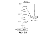
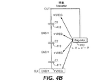
図3A、図3Bおよび図4A、図4Bに1組の例示的な実施形態を示す。いずれの場合も、移動段階またはモードでは、複数(N個、ここではN=3個)のコンデンサが直列に接続され、初期化段階またはモードでは、低電圧レベル(通常は接地)とレギュレータ電圧との間でそれぞれのコンデンサが接続される。レギュレータ電圧はフィードバックに基づきレギュレータ回路から提供され、各内部ステージノードのプレチャージ制御に役立てることができる。 A set of exemplary embodiments is shown in FIGS. 3A, 3B and 4A, 4B. In any case, a plurality (N, here N = 3) of capacitors are connected in series in the moving phase or mode, and in the initialization phase or mode, the low voltage level (usually ground), the regulator voltage, Each capacitor is connected between. The regulator voltage is provided from the regulator circuit based on feedback and can be used for precharge control of each internal stage node.
図3Aおよび図3Bは、第1の実施形態のチャージポンプの初期化段階と移動段階をそれぞれ示している。これらの例に見られるステージ数Nは便宜上N=3だが、これ以外の数でも適宜使用できることが理解できるはずである。図3Aの初期化段階で各コンデンサの「下」極板(C1 311、C2 313、C3 315)は0Vに設定され、「上」極板は調整済み電圧Vregに基づくレベルにリセットされる。Vregはレギュレータ303から供給され、クロック信号CLKに基づきこれを果たすスイッチは模式的に図に示されている。スイッチとレギュレータ回路はいずれも当該技術分野で公知の標準的技術で実施できる。
3A and 3B respectively show the initialization stage and the movement stage of the charge pump of the first embodiment. The number of stages N seen in these examples is N = 3 for convenience, but it should be understood that other numbers can be used as appropriate. In the initialization phase of FIG. 3A, the “lower” plate (
図3Bには第2の作動段階、すなわち移動段階が示される。N個のステージは、電圧源からのVddレベルと出力を供給する出力ノードとの間で直列に接続されている。この出力はレギュレータ303にも供給される。このため、調整フィードバックをもとに内部ステージノードのプレチャージレベルを制御でき(図3Aで説明)、クロックはVddレベルで常時作動できる。出力はVout=N*K*Vreg+Vddまで上昇する。Kは、作動時の電荷共有効率に基づく係数である。これはスイッチ(模式的に図に示す)にまたがるいかなる降下も無視した理想的レベルである。好ましくは、いかなる降下も最小限に抑えるレベルでスイッチを駆動する。上極板にVddを印加するだけでなく、初期化段階に調整電圧を使って上極板をプレチャージすることにより、調整された出力を得ることができ、図3Bの直列構成で高電力効率および高電流要求が達成される。
FIG. 3B shows the second operating phase, ie the moving phase. The N stages are connected in series between the Vdd level from the voltage source and the output node that provides the output. This output is also supplied to the
図4Aおよび図4Bは、チャージポンプの代替の実施形態の初期化段階と移動段階をそれぞれ示している。種々の素子は、図3Aおよび図3Bと同様にラベル付けされ、同様の働きをする。主な違いとして、クロック振幅のみならず内部ステージノードのプレチャージレベル制御に調整フィードバックを役立てることができることが挙げられる。図4Bの移動段階では、VddではなくVregと出力ノードとの間でコンデンサが直列に接続される。その結果、出力電圧は(理想的には)Vout=N*K*Vreg+Vregまで上昇する。この場合にはレギュレータ回路403からのフィードバックによって全ての出力電圧を調整できる。
4A and 4B show the initialization and transfer phases, respectively, of an alternative embodiment of the charge pump. The various elements are labeled and function similarly as in FIGS. 3A and 3B. The main difference is that adjustment feedback can be used not only for clock amplitude but also for precharge level control of internal stage nodes. 4B, a capacitor is connected in series between Vreg and the output node instead of Vdd. As a result, the output voltage rises (ideally) to Vout = N * K * Vreg + Vreg. In this case, all output voltages can be adjusted by feedback from the
正の電圧出力を生成する場合について、図3A、図3Bおよび図4A、図4Bの構成を説明したが、同様の構成で負の電圧を生成することもできる。さらに具体的には、それには、簡潔に述べれば図3A、図3Bおよび図4A、図4Bの実施形態を接続の点で「逆さ」にし、対応する負の調整電圧を使用すればよい。 In the case of generating a positive voltage output, the configurations of FIGS. 3A, 3B, 4A, and 4B have been described, but a negative voltage can also be generated with a similar configuration. More specifically, it can be briefly described by making the embodiments of FIGS. 3A, 3B and 4A, 4B “inverted” in terms of connection and using a corresponding negative adjustment voltage.
これまで特定の実施形態を参照しながら本発明を説明してきたが、この説明は本発明の一応用例に過ぎず、制限として解釈すべきものではない。開示した実施形態の特徴の様々な適応ならびに組み合わせは、添付の特許請求の範囲によって規定される本発明の範囲内にある。 Although the present invention has been described with reference to particular embodiments, this description is only an example of the invention's application and should not be construed as limiting. Various adaptations and combinations of the features of the disclosed embodiments are within the scope of the invention as defined by the appended claims.
Claims (7)
第1の極板と第2の極板とを各々有する複数のコンデンサと、
切替回路であって、それによってコンデンサは第1の段階と第2の段階とで交互に接続され、第1の段階ではコンデンサの第1の極板がレギュレータ電圧を受け取るように接続され、コンデンサの第2の極板は接地へ接続され、第2の段階ではコンデンサが直列に接続され、直列内の第1のコンデンサより後ろの各コンデンサでは第2の極板が直列内の先行コンデンサの第1の極板へ接続され、最終コンデンサの第1の極板はチャージポンプ回路の出力電圧を供給するように接続される切替回路と、
基準電圧とチャージポンプからの出力電圧を受け取り、かつ前記基準電圧からレギュレータ電圧を生成するように接続可能な調整回路であって、レギュレータ電圧値は出力電圧レベルに応答する調整回路と、
を備えるチャージポンプ回路。 A charge pump circuit for generating an output voltage,
A plurality of capacitors each having a first electrode plate and a second electrode plate;
A switching circuit, whereby the capacitors are alternately connected in the first stage and the second stage, and in the first stage, the first plate of the capacitor is connected to receive the regulator voltage; The second plate is connected to ground, in the second stage a capacitor is connected in series, and for each capacitor behind the first capacitor in the series, the second plate is the first of the preceding capacitors in the series. A switching circuit connected to supply the output voltage of the charge pump circuit; and
An adjustment circuit that is connectable to receive a reference voltage and an output voltage from a charge pump and to generate a regulator voltage from the reference voltage, the regulator voltage value being an adjustment circuit responsive to the output voltage level;
A charge pump circuit comprising:
直列内の第1のコンデンサの第2の極板は、第2の段階中に電圧源から電圧レベルを受け取るように接続されるチャージポンプ回路。 The charge pump circuit according to claim 1, wherein
A charge pump circuit in which the second plate of the first capacitor in series is connected to receive a voltage level from a voltage source during the second stage.
直列内の第1のコンデンサの第2の極板は、第2の段階中にレギュレータ電圧を受け取るように接続されるチャージポンプ回路。 The charge pump circuit according to claim 1, wherein
A charge pump circuit, wherein the second plate of the first capacitor in the series is connected to receive the regulator voltage during the second stage.
チャージポンプ回路は、不揮発性メモリ回路上の周辺回路の一部であるチャージポンプ回路。 The charge pump circuit according to claim 1, wherein
The charge pump circuit is a charge pump circuit that is a part of a peripheral circuit on the nonvolatile memory circuit.
第1の極板と第2の極板とを各々有する複数のコンデンサを設けるステップと、
第1の段階と第2の段階とで交互にコンデンサを接続するステップであって、前記第1の段階は、
レギュレータ電圧を受け取るようにコンデンサの第1の極板を接続することと、
第2の極板を接地へ接続することと、を含み、前記第2の段階は、
直列内の第1のコンデンサより後ろの各コンデンサでは第2の極板が直列内の先行コンデンサの第1の極板へ接続されるように直列のコンデンサを接続することと、
直列内の最終コンデンサの第1の極板からチャージポンプ回路の出力電圧を供給することと、を含む接続するステップと、
基準電圧から調整電圧を生成するステップであって、レギュレータ電圧値は出力電圧レベルに応答する生成するステップと、
を含む方法。 A method for generating an output voltage comprising:
Providing a plurality of capacitors each having a first electrode plate and a second electrode plate;
Alternately connecting capacitors in the first stage and the second stage, wherein the first stage comprises:
Connecting the first plate of the capacitor to receive the regulator voltage;
Connecting the second plate to ground, the second stage comprising:
Connecting a series capacitor so that for each capacitor behind the first capacitor in the series, the second plate is connected to the first plate of the preceding capacitor in the series;
Providing an output voltage of a charge pump circuit from a first plate of a final capacitor in series, and connecting
Generating a regulated voltage from a reference voltage, wherein a regulator voltage value is generated in response to an output voltage level;
Including methods.
前記第2の段階は、電圧源から電圧レベルを受け取るように直列内の第1のコンデンサを接続することをさらに含む方法。 The method of claim 5, wherein
The second step further comprises connecting a first capacitor in series to receive a voltage level from a voltage source.
前記第2の段階は、レギュレータ電圧を受け取るように直列内の第1のコンデンサを接続することをさらに含む方法。 The method of claim 5, wherein
The method further comprising connecting a first capacitor in series to receive the regulator voltage.
Applications Claiming Priority (2)
| Application Number | Priority Date | Filing Date | Title |
|---|---|---|---|
| US11/955,221 US7586362B2 (en) | 2007-12-12 | 2007-12-12 | Low voltage charge pump with regulation |
| PCT/US2008/085827 WO2009076277A1 (en) | 2007-12-12 | 2008-12-08 | Low voltage charge pump with regulation |
Publications (2)
| Publication Number | Publication Date |
|---|---|
| JP2011507471A true JP2011507471A (en) | 2011-03-03 |
| JP2011507471A5 JP2011507471A5 (en) | 2011-12-15 |
Family
ID=40506475
Family Applications (1)
| Application Number | Title | Priority Date | Filing Date |
|---|---|---|---|
| JP2010538076A Pending JP2011507471A (en) | 2007-12-12 | 2008-12-08 | Adjustable low voltage charge pump |
Country Status (7)
| Country | Link |
|---|---|
| US (1) | US7586362B2 (en) |
| EP (1) | EP2223419A1 (en) |
| JP (1) | JP2011507471A (en) |
| KR (1) | KR20100099685A (en) |
| CN (1) | CN101897110A (en) |
| TW (1) | TWI463774B (en) |
| WO (1) | WO2009076277A1 (en) |
Families Citing this family (49)
| Publication number | Priority date | Publication date | Assignee | Title |
|---|---|---|---|---|
| US7880531B2 (en) * | 2008-01-23 | 2011-02-01 | Micron Technology, Inc. | System, apparatus, and method for selectable voltage regulation |
| US7969235B2 (en) | 2008-06-09 | 2011-06-28 | Sandisk Corporation | Self-adaptive multi-stage charge pump |
| US8710907B2 (en) * | 2008-06-24 | 2014-04-29 | Sandisk Technologies Inc. | Clock generator circuit for a charge pump |
| US7973592B2 (en) * | 2009-07-21 | 2011-07-05 | Sandisk Corporation | Charge pump with current based regulation |
| US8339183B2 (en) * | 2009-07-24 | 2012-12-25 | Sandisk Technologies Inc. | Charge pump with reduced energy consumption through charge sharing and clock boosting suitable for high voltage word line in flash memories |
| US20110148509A1 (en) * | 2009-12-17 | 2011-06-23 | Feng Pan | Techniques to Reduce Charge Pump Overshoot |
| US8305807B2 (en) | 2010-07-09 | 2012-11-06 | Sandisk Technologies Inc. | Detection of broken word-lines in memory arrays |
| US8432732B2 (en) | 2010-07-09 | 2013-04-30 | Sandisk Technologies Inc. | Detection of word-line leakage in memory arrays |
| US8514630B2 (en) | 2010-07-09 | 2013-08-20 | Sandisk Technologies Inc. | Detection of word-line leakage in memory arrays: current based approach |
| US8106701B1 (en) | 2010-09-30 | 2012-01-31 | Sandisk Technologies Inc. | Level shifter with shoot-through current isolation |
| US8294509B2 (en) | 2010-12-20 | 2012-10-23 | Sandisk Technologies Inc. | Charge pump systems with reduction in inefficiencies due to charge sharing between capacitances |
| US8339185B2 (en) | 2010-12-20 | 2012-12-25 | Sandisk 3D Llc | Charge pump system that dynamically selects number of active stages |
| US8537593B2 (en) | 2011-04-28 | 2013-09-17 | Sandisk Technologies Inc. | Variable resistance switch suitable for supplying high voltage to drive load |
| US8379454B2 (en) | 2011-05-05 | 2013-02-19 | Sandisk Technologies Inc. | Detection of broken word-lines in memory arrays |
| US8726104B2 (en) | 2011-07-28 | 2014-05-13 | Sandisk Technologies Inc. | Non-volatile memory and method with accelerated post-write read using combined verification of multiple pages |
| US8750042B2 (en) | 2011-07-28 | 2014-06-10 | Sandisk Technologies Inc. | Combined simultaneous sensing of multiple wordlines in a post-write read (PWR) and detection of NAND failures |
| US8775901B2 (en) | 2011-07-28 | 2014-07-08 | SanDisk Technologies, Inc. | Data recovery for defective word lines during programming of non-volatile memory arrays |
| US8699247B2 (en) | 2011-09-09 | 2014-04-15 | Sandisk Technologies Inc. | Charge pump system dynamically reconfigurable for read and program |
| US8514628B2 (en) | 2011-09-22 | 2013-08-20 | Sandisk Technologies Inc. | Dynamic switching approach to reduce area and power consumption of high voltage charge pumps |
| US8400212B1 (en) | 2011-09-22 | 2013-03-19 | Sandisk Technologies Inc. | High voltage charge pump regulation system with fine step adjustment |
| US8395434B1 (en) | 2011-10-05 | 2013-03-12 | Sandisk Technologies Inc. | Level shifter with negative voltage capability |
| US8730722B2 (en) | 2012-03-02 | 2014-05-20 | Sandisk Technologies Inc. | Saving of data in cases of word-line to word-line short in memory arrays |
| US8710909B2 (en) | 2012-09-14 | 2014-04-29 | Sandisk Technologies Inc. | Circuits for prevention of reverse leakage in Vth-cancellation charge pumps |
| US9810723B2 (en) | 2012-09-27 | 2017-11-07 | Sandisk Technologies Llc | Charge pump based over-sampling ADC for current detection |
| US9164526B2 (en) | 2012-09-27 | 2015-10-20 | Sandisk Technologies Inc. | Sigma delta over-sampling charge pump analog-to-digital converter |
| US8836412B2 (en) | 2013-02-11 | 2014-09-16 | Sandisk 3D Llc | Charge pump with a power-controlled clock buffer to reduce power consumption and output voltage ripple |
| US8981835B2 (en) | 2013-06-18 | 2015-03-17 | Sandisk Technologies Inc. | Efficient voltage doubler |
| US9024680B2 (en) | 2013-06-24 | 2015-05-05 | Sandisk Technologies Inc. | Efficiency for charge pumps with low supply voltages |
| US9077238B2 (en) | 2013-06-25 | 2015-07-07 | SanDisk Technologies, Inc. | Capacitive regulation of charge pumps without refresh operation interruption |
| US9007046B2 (en) | 2013-06-27 | 2015-04-14 | Sandisk Technologies Inc. | Efficient high voltage bias regulation circuit |
| US9165683B2 (en) | 2013-09-23 | 2015-10-20 | Sandisk Technologies Inc. | Multi-word line erratic programming detection |
| US9083231B2 (en) | 2013-09-30 | 2015-07-14 | Sandisk Technologies Inc. | Amplitude modulation for pass gate to improve charge pump efficiency |
| US9154027B2 (en) | 2013-12-09 | 2015-10-06 | Sandisk Technologies Inc. | Dynamic load matching charge pump for reduced current consumption |
| US9653126B2 (en) | 2014-01-27 | 2017-05-16 | Sandisk Technologies Llc | Digital ramp rate control for charge pumps |
| US9443612B2 (en) | 2014-07-10 | 2016-09-13 | Sandisk Technologies Llc | Determination of bit line to low voltage signal shorts |
| US9514835B2 (en) | 2014-07-10 | 2016-12-06 | Sandisk Technologies Llc | Determination of word line to word line shorts between adjacent blocks |
| US9484086B2 (en) | 2014-07-10 | 2016-11-01 | Sandisk Technologies Llc | Determination of word line to local source line shorts |
| US9460809B2 (en) | 2014-07-10 | 2016-10-04 | Sandisk Technologies Llc | AC stress mode to screen out word line to word line shorts |
| US9330776B2 (en) | 2014-08-14 | 2016-05-03 | Sandisk Technologies Inc. | High voltage step down regulator with breakdown protection |
| US9202593B1 (en) | 2014-09-02 | 2015-12-01 | Sandisk Technologies Inc. | Techniques for detecting broken word lines in non-volatile memories |
| US9240249B1 (en) | 2014-09-02 | 2016-01-19 | Sandisk Technologies Inc. | AC stress methods to screen out bit line defects |
| US9449694B2 (en) | 2014-09-04 | 2016-09-20 | Sandisk Technologies Llc | Non-volatile memory with multi-word line select for defect detection operations |
| US9917507B2 (en) | 2015-05-28 | 2018-03-13 | Sandisk Technologies Llc | Dynamic clock period modulation scheme for variable charge pump load currents |
| US9647536B2 (en) | 2015-07-28 | 2017-05-09 | Sandisk Technologies Llc | High voltage generation using low voltage devices |
| US9659666B2 (en) | 2015-08-31 | 2017-05-23 | Sandisk Technologies Llc | Dynamic memory recovery at the sub-block level |
| US9520776B1 (en) | 2015-09-18 | 2016-12-13 | Sandisk Technologies Llc | Selective body bias for charge pump transfer switches |
| CN105529917A (en) * | 2016-01-21 | 2016-04-27 | 中山芯达电子科技有限公司 | High efficiency fast voltage generating circuit |
| US9698676B1 (en) | 2016-03-11 | 2017-07-04 | Sandisk Technologies Llc | Charge pump based over-sampling with uniform step size for current detection |
| CN109565243B (en) | 2016-08-05 | 2022-02-25 | 香港大学 | High efficiency switched capacitor power supply and method |
Citations (2)
| Publication number | Priority date | Publication date | Assignee | Title |
|---|---|---|---|---|
| JP2007020268A (en) * | 2005-07-06 | 2007-01-25 | Casio Comput Co Ltd | Power supply circuit |
| JP2007202267A (en) * | 2006-01-25 | 2007-08-09 | Rohm Co Ltd | Power supply device and electrical apparatus using the same |
Family Cites Families (64)
| Publication number | Priority date | Publication date | Assignee | Title |
|---|---|---|---|---|
| US3697860A (en) | 1971-03-15 | 1972-10-10 | Westinghouse Electric Corp | Dc static switch circuit with a main switch device and a power sharing circuit portion |
| US4511811A (en) | 1982-02-08 | 1985-04-16 | Seeq Technology, Inc. | Charge pump for providing programming voltage to the word lines in a semiconductor memory array |
| US4583157A (en) | 1985-02-08 | 1986-04-15 | At&T Bell Laboratories | Integrated circuit having a variably boosted node |
| US4636748A (en) | 1985-06-26 | 1987-01-13 | Data General Corporation | Charge pump for use in a phase-locked loop |
| US4736121A (en) | 1985-09-10 | 1988-04-05 | Sos Microelettronica S.p.A. | Charge pump circuit for driving N-channel MOS transistors |
| US4888738A (en) | 1988-06-29 | 1989-12-19 | Seeq Technology | Current-regulated, voltage-regulated erase circuit for EEPROM memory |
| US5392205A (en) | 1991-11-07 | 1995-02-21 | Motorola, Inc. | Regulated charge pump and method therefor |
| US5436587A (en) | 1993-11-24 | 1995-07-25 | Sundisk Corporation | Charge pump circuit with exponetral multiplication |
| US5508971A (en) | 1994-10-17 | 1996-04-16 | Sandisk Corporation | Programmable power generation circuit for flash EEPROM memory systems |
| US5563779A (en) | 1994-12-05 | 1996-10-08 | Motorola, Inc. | Method and apparatus for a regulated supply on an integrated circuit |
| US5596532A (en) | 1995-10-18 | 1997-01-21 | Sandisk Corporation | Flash EEPROM self-adaptive voltage generation circuit operative within a continuous voltage source range |
| DE19612443C2 (en) | 1996-03-28 | 1998-02-05 | Siemens Ag | Circuit arrangement for supplying an electronic load circuit |
| US5625544A (en) | 1996-04-25 | 1997-04-29 | Programmable Microelectronics Corp. | Charge pump |
| JP2917914B2 (en) | 1996-05-17 | 1999-07-12 | 日本電気株式会社 | Boost circuit |
| US5818288A (en) | 1996-06-27 | 1998-10-06 | Advanced Micro Devices, Inc. | Charge pump circuit having non-uniform stage capacitance for providing increased rise time and reduced area |
| US5818289A (en) | 1996-07-18 | 1998-10-06 | Micron Technology, Inc. | Clocking scheme and charge transfer switch for increasing the efficiency of a charge pump or other circuit |
| US6023187A (en) | 1997-12-23 | 2000-02-08 | Mitsubishi Semiconductor America, Inc. | Voltage pump for integrated circuit and operating method thereof |
| KR100273278B1 (en) | 1998-02-11 | 2001-01-15 | 김영환 | Pumping circuit of semiconductor memory device |
| US6606267B2 (en) | 1998-06-23 | 2003-08-12 | Sandisk Corporation | High data rate write process for non-volatile flash memories |
| US5969986A (en) | 1998-06-23 | 1999-10-19 | Invox Technology | High-bandwidth read and write architectures for non-volatile memories |
| US6404274B1 (en) | 1998-04-09 | 2002-06-11 | Kabushiki Kaisha Toshiba | Internal voltage generating circuit capable of generating variable multi-level voltages |
| US6344959B1 (en) | 1998-05-01 | 2002-02-05 | Unitrode Corporation | Method for sensing the output voltage of a charge pump circuit without applying a load to the output stage |
| EP0971361B1 (en) | 1998-06-23 | 2003-12-10 | SanDisk Corporation | High data rate write process for non-volatile flash memories |
| US6208542B1 (en) | 1998-06-30 | 2001-03-27 | Sandisk Corporation | Techniques for storing digital data in an analog or multilevel memory |
| US6249898B1 (en) | 1998-06-30 | 2001-06-19 | Synopsys, Inc. | Method and system for reliability analysis of CMOS VLSI circuits based on stage partitioning and node activities |
| US6198645B1 (en) * | 1998-07-02 | 2001-03-06 | National Semiconductor Corporation | Buck and boost switched capacitor gain stage with optional shared rest state |
| JP3237654B2 (en) | 1999-05-19 | 2001-12-10 | 日本電気株式会社 | Semiconductor device |
| US6169444B1 (en) | 1999-07-15 | 2001-01-02 | Maxim Integrated Products, Inc. | Pulse frequency operation of regulated charge pumps |
| JP2001075536A (en) | 1999-09-03 | 2001-03-23 | Nec Corp | Booster circuit, source circuit and liquid crystal drive device |
| TW578377B (en) * | 2000-05-10 | 2004-03-01 | Sanyo Electric Co | Charge-pump circuit and method for controlling the same |
| EP1184962B1 (en) | 2000-08-22 | 2006-05-17 | STMicroelectronics S.r.l. | High efficiency electronic circuit for generating and regulating a supply voltage |
| US6525949B1 (en) | 2000-12-22 | 2003-02-25 | Matrix Semiconductor, Inc. | Charge pump circuit |
| US6577535B2 (en) | 2001-02-16 | 2003-06-10 | Sandisk Corporation | Method and system for distributed power generation in multi-chip memory systems |
| US6486728B2 (en) | 2001-03-16 | 2002-11-26 | Matrix Semiconductor, Inc. | Multi-stage charge pump |
| JP2002315308A (en) * | 2001-04-10 | 2002-10-25 | Fujitsu Ltd | Dc-dc converter and memory thereof |
| US6424570B1 (en) | 2001-06-26 | 2002-07-23 | Advanced Micro Devices, Inc. | Modulated charge pump with uses an analog to digital converter to compensate for supply voltage variations |
| JP4152094B2 (en) | 2001-09-03 | 2008-09-17 | エルピーダメモリ株式会社 | Semiconductor memory device control method and semiconductor memory device |
| JP3557186B2 (en) * | 2001-09-26 | 2004-08-25 | 三洋電機株式会社 | DC-DC converter |
| JP4222768B2 (en) | 2002-03-27 | 2009-02-12 | 三洋電機株式会社 | Booster and imaging device using the same |
| US6861894B2 (en) | 2002-09-27 | 2005-03-01 | Sandisk Corporation | Charge pump with Fibonacci number multiplication |
| ITMI20022268A1 (en) | 2002-10-25 | 2004-04-26 | Atmel Corp | VARIABLE CHARGE PUMP CIRCUIT WITH DYNAMIC LOAD |
| US6975135B1 (en) | 2002-12-10 | 2005-12-13 | Altera Corporation | Universally programmable output buffer |
| US6734718B1 (en) | 2002-12-23 | 2004-05-11 | Sandisk Corporation | High voltage ripple reduction |
| US6891764B2 (en) | 2003-04-11 | 2005-05-10 | Intel Corporation | Apparatus and method to read a nonvolatile memory |
| US7023260B2 (en) | 2003-06-30 | 2006-04-04 | Matrix Semiconductor, Inc. | Charge pump circuit incorporating corresponding parallel charge pump stages and method therefor |
| FR2858725B1 (en) | 2003-08-06 | 2005-10-07 | St Microelectronics Sa | SELF-PORTABLE DEVICE FOR GENERATING A HIGH VOLTAGE, AND METHOD FOR REPAIRING A DEVICE FOR GENERATING A HIGH VOLTAGE. |
| US6922096B2 (en) | 2003-08-07 | 2005-07-26 | Sandisk Corporation | Area efficient charge pump |
| US6859091B1 (en) | 2003-09-18 | 2005-02-22 | Maxim Integrated Products, Inc. | Continuous linear regulated zero dropout charge pump with high efficiency load predictive clocking scheme |
| US7030683B2 (en) | 2004-05-10 | 2006-04-18 | Sandisk Corporation | Four phase charge pump operable without phase overlap with improved efficiency |
| JP2006158132A (en) | 2004-11-30 | 2006-06-15 | Renesas Technology Corp | Charge-pump power supply circuit |
| GB2434675B (en) | 2004-11-30 | 2010-01-06 | Spansion Japan Ltd | Semiconductor device and semiconductor control method |
| US7120051B2 (en) | 2004-12-14 | 2006-10-10 | Sandisk Corporation | Pipelined programming of non-volatile memories using early data |
| TWI298828B (en) | 2005-06-29 | 2008-07-11 | Novatek Microelectronics Corp | Charge pump for generating arbitrary voltage level |
| US7276960B2 (en) | 2005-07-18 | 2007-10-02 | Dialog Semiconductor Gmbh | Voltage regulated charge pump with regulated charge current into the flying capacitor |
| US20070126494A1 (en) | 2005-12-06 | 2007-06-07 | Sandisk Corporation | Charge pump having shunt diode for improved operating efficiency |
| US20070139099A1 (en) | 2005-12-16 | 2007-06-21 | Sandisk Corporation | Charge pump regulation control for improved power efficiency |
| US7372320B2 (en) | 2005-12-16 | 2008-05-13 | Sandisk Corporation | Voltage regulation with active supplemental current for output stabilization |
| US7397677B1 (en) | 2006-02-08 | 2008-07-08 | National Semiconductor Corporation | Apparatus and method for charge pump control with adjustable series resistance |
| US20070229149A1 (en) | 2006-03-30 | 2007-10-04 | Sandisk Corporation | Voltage regulator having high voltage protection |
| US7554311B2 (en) | 2006-07-31 | 2009-06-30 | Sandisk Corporation | Hybrid charge pump regulation |
| US7440342B2 (en) | 2006-12-29 | 2008-10-21 | Sandisk Corporation | Unified voltage generation method with improved power efficiency |
| US7477092B2 (en) | 2006-12-29 | 2009-01-13 | Sandisk Corporation | Unified voltage generation apparatus with improved power efficiency |
| US7558129B2 (en) | 2007-03-30 | 2009-07-07 | Sandisk 3D Llc | Device with load-based voltage generation |
| US7515488B2 (en) | 2007-03-30 | 2009-04-07 | Sandisk 3D Llc | Method for load-based voltage generation |
-
2007
- 2007-12-12 US US11/955,221 patent/US7586362B2/en not_active Expired - Fee Related
-
2008
- 2008-12-08 EP EP08860541A patent/EP2223419A1/en not_active Withdrawn
- 2008-12-08 WO PCT/US2008/085827 patent/WO2009076277A1/en active Application Filing
- 2008-12-08 CN CN2008801206856A patent/CN101897110A/en active Pending
- 2008-12-08 JP JP2010538076A patent/JP2011507471A/en active Pending
- 2008-12-08 KR KR1020107011587A patent/KR20100099685A/en not_active Application Discontinuation
- 2008-12-12 TW TW097148610A patent/TWI463774B/en not_active IP Right Cessation
Patent Citations (2)
| Publication number | Priority date | Publication date | Assignee | Title |
|---|---|---|---|---|
| JP2007020268A (en) * | 2005-07-06 | 2007-01-25 | Casio Comput Co Ltd | Power supply circuit |
| JP2007202267A (en) * | 2006-01-25 | 2007-08-09 | Rohm Co Ltd | Power supply device and electrical apparatus using the same |
Also Published As
| Publication number | Publication date |
|---|---|
| US7586362B2 (en) | 2009-09-08 |
| CN101897110A (en) | 2010-11-24 |
| US20090153230A1 (en) | 2009-06-18 |
| EP2223419A1 (en) | 2010-09-01 |
| WO2009076277A1 (en) | 2009-06-18 |
| KR20100099685A (en) | 2010-09-13 |
| TWI463774B (en) | 2014-12-01 |
| TW200937819A (en) | 2009-09-01 |
Similar Documents
| Publication | Publication Date | Title |
|---|---|---|
| JP2011507471A (en) | Adjustable low voltage charge pump | |
| JP4209878B2 (en) | Charge pump circuit and DC converter using the same | |
| US8044705B2 (en) | Bottom plate regulation of charge pumps | |
| US7683700B2 (en) | Techniques of ripple reduction for charge pumps | |
| US8699247B2 (en) | Charge pump system dynamically reconfigurable for read and program | |
| Pelliconi et al. | Power efficient charge pump in deep submicron standard CMOS technology | |
| US7579902B2 (en) | Charge pump for generation of multiple output-voltage levels | |
| JP4336489B2 (en) | Semiconductor integrated circuit | |
| US20090315616A1 (en) | Clock Generator Circuit for a Charge Pump | |
| US9077238B2 (en) | Capacitive regulation of charge pumps without refresh operation interruption | |
| TW200934079A (en) | Diode connected regulation of charge pumps | |
| US8896367B1 (en) | Charge pump system | |
| JPH11273378A (en) | High voltage generating circuit | |
| JP2009509481A (en) | Efficient charge pump for a wide range of supply voltages | |
| JP2009060702A (en) | Charge pump booster circuit | |
| JP2007089242A (en) | Semiconductor device with charge pump booster circuit | |
| US20090302930A1 (en) | Charge Pump with Vt Cancellation Through Parallel Structure | |
| JP3475173B2 (en) | Charge pump circuit | |
| US20140232452A1 (en) | Internal voltage generation circuit | |
| JP2011087385A (en) | Charge pump circuit | |
| Rana et al. | Single charge-pump generating high positive and negative voltages driving common load | |
| JP3713267B2 (en) | Charge pump circuit | |
| JP2006280160A (en) | Charge pump circuit | |
| JP2005117830A (en) | Charge pump circuit | |
| Rana | Area efficient NMOS based positive and negative voltage multiplier |
Legal Events
| Date | Code | Title | Description |
|---|---|---|---|
| A521 | Request for written amendment filed |
Free format text: JAPANESE INTERMEDIATE CODE: A523 Effective date: 20111026 |
|
| A621 | Written request for application examination |
Free format text: JAPANESE INTERMEDIATE CODE: A621 Effective date: 20111026 |
|
| A871 | Explanation of circumstances concerning accelerated examination |
Free format text: JAPANESE INTERMEDIATE CODE: A871 Effective date: 20111026 |
|
| A975 | Report on accelerated examination |
Free format text: JAPANESE INTERMEDIATE CODE: A971005 Effective date: 20111201 |
|
| A131 | Notification of reasons for refusal |
Free format text: JAPANESE INTERMEDIATE CODE: A131 Effective date: 20111206 |
|
| A601 | Written request for extension of time |
Free format text: JAPANESE INTERMEDIATE CODE: A601 Effective date: 20120223 |
|
| A602 | Written permission of extension of time |
Free format text: JAPANESE INTERMEDIATE CODE: A602 Effective date: 20120301 |
|
| A02 | Decision of refusal |
Free format text: JAPANESE INTERMEDIATE CODE: A02 Effective date: 20120731 |