JP2006158132A - Charge-pump power supply circuit - Google Patents
Charge-pump power supply circuit Download PDFInfo
- Publication number
- JP2006158132A JP2006158132A JP2004347520A JP2004347520A JP2006158132A JP 2006158132 A JP2006158132 A JP 2006158132A JP 2004347520 A JP2004347520 A JP 2004347520A JP 2004347520 A JP2004347520 A JP 2004347520A JP 2006158132 A JP2006158132 A JP 2006158132A
- Authority
- JP
- Japan
- Prior art keywords
- charge pump
- voltage
- charging
- switches
- circuit
- Prior art date
- Legal status (The legal status is an assumption and is not a legal conclusion. Google has not performed a legal analysis and makes no representation as to the accuracy of the status listed.)
- Pending
Links
- 239000003990 capacitor Substances 0.000 claims abstract description 97
- 230000000087 stabilizing effect Effects 0.000 abstract description 5
- 238000010586 diagram Methods 0.000 description 16
- 238000001514 detection method Methods 0.000 description 13
- 230000007274 generation of a signal involved in cell-cell signaling Effects 0.000 description 12
- 238000007599 discharging Methods 0.000 description 11
- 230000015556 catabolic process Effects 0.000 description 5
- 238000012544 monitoring process Methods 0.000 description 5
- 230000000694 effects Effects 0.000 description 4
- 238000000034 method Methods 0.000 description 2
- 230000006641 stabilisation Effects 0.000 description 2
- 238000011105 stabilization Methods 0.000 description 2
Images


Classifications
-
- H—ELECTRICITY
- H02—GENERATION; CONVERSION OR DISTRIBUTION OF ELECTRIC POWER
- H02M—APPARATUS FOR CONVERSION BETWEEN AC AND AC, BETWEEN AC AND DC, OR BETWEEN DC AND DC, AND FOR USE WITH MAINS OR SIMILAR POWER SUPPLY SYSTEMS; CONVERSION OF DC OR AC INPUT POWER INTO SURGE OUTPUT POWER; CONTROL OR REGULATION THEREOF
- H02M3/00—Conversion of dc power input into dc power output
- H02M3/02—Conversion of dc power input into dc power output without intermediate conversion into ac
- H02M3/04—Conversion of dc power input into dc power output without intermediate conversion into ac by static converters
- H02M3/06—Conversion of dc power input into dc power output without intermediate conversion into ac by static converters using resistors or capacitors, e.g. potential divider
- H02M3/07—Conversion of dc power input into dc power output without intermediate conversion into ac by static converters using resistors or capacitors, e.g. potential divider using capacitors charged and discharged alternately by semiconductor devices with control electrode, e.g. charge pumps
Abstract
Description
この発明は、コンデンサの充放電によって入力電圧を昇圧して出力するチャージポンプ方式電源回路に関し、特に多段に縦属接続して高電圧を得るチャージポンプ方式電源回路に関するものである。 The present invention relates to a charge pump type power supply circuit that boosts and outputs an input voltage by charging and discharging a capacitor, and more particularly to a charge pump type power supply circuit that obtains a high voltage by cascade connection in multiple stages.
チャージポンプ方式電源回路は、一般に、充電路と放電路を構成するスイッチにMOSトランジスタを用い、入力電源を充電路から充電コンデンサに印加して電荷を蓄積し、さらに入力電源を放電路から充電用コンデンサに印加して充電電荷に加算し、その加算電荷を出力用コンデンサに移すことで、電圧の昇圧を行っている(例えば特許文献1,2)。この場合、得られる昇圧電圧は入力電圧の2倍であるので、さらに高い電圧を得ようとする場合は、多段に縦属接続した構成が採用されている。以下、この発明の理解を容易にするために、2段構成のチャージポンプ方式電源回路について説明する。
In general, a charge pump type power supply circuit uses a MOS transistor as a switch constituting a charging path and a discharging path, applies charge from the charging path to a charging capacitor, accumulates charge, and further charges the input power from the discharging path. The voltage is boosted by applying it to the capacitor and adding it to the charge, and transferring the added charge to the output capacitor (for example,
図8は、従来技術による2段構成のチャージポンプ方式電源回路の基本構成を示す回路図である。図8において、初段のチャージポンプ方式電源回路(以降、単に「チャージポンプ回路」と記す)CP1と2段目のチャージポンプ回路CP2は、同様の構成である。チャージポンプ回路CP1では、充電路を構成するスイッチ(PMOSトランジスタQ11,NMOSトランジスタQ12)と、放電路を構成するスイッチ(NMOSトランジスタQ13,PMOSトランジスタQ14)と、充電用コンデンサC11と、出力用コンデンサC12とを備えている。 FIG. 8 is a circuit diagram showing a basic configuration of a two-stage charge pump power supply circuit according to the prior art. In FIG. 8, the first-stage charge pump power supply circuit (hereinafter simply referred to as “charge pump circuit”) CP1 and the second-stage charge pump circuit CP2 have the same configuration. In the charge pump circuit CP1, switches (PMOS transistor Q11, NMOS transistor Q12) constituting a charging path, switches (NMOS transistors Q13, PMOS transistor Q14) constituting a discharging path, a charging capacitor C11, and an output capacitor C12 And.
チャージポンプ回路CP1の充電側では、PMOSトランジスタQ11のソース電極は入力電圧Vinが印加され、PMOSトランジスタQ11のドレイン電極は充電用コンデンサC11の一方の電極に接続されている。NMOSトランジスタQ12のドレイン電極は充電用コンデンサC11の他方の電極に接続され、NMOSトランジスタQ12のソース電極は接地(グランド)に接続されている。そして、図示しない制御回路が発生する充電制御信号TC1が、NMOSトランジスタQ12のゲート電極に直接印加されるとともに、インバータQ51を介してPMOSトランジスタQ11のゲート電極に印加される。 On the charging side of the charge pump circuit CP1, the input voltage Vin is applied to the source electrode of the PMOS transistor Q11, and the drain electrode of the PMOS transistor Q11 is connected to one electrode of the charging capacitor C11. The drain electrode of the NMOS transistor Q12 is connected to the other electrode of the charging capacitor C11, and the source electrode of the NMOS transistor Q12 is connected to the ground (ground). A charge control signal TC1 generated by a control circuit (not shown) is directly applied to the gate electrode of the NMOS transistor Q12 and is also applied to the gate electrode of the PMOS transistor Q11 via the inverter Q51.
チャージポンプ回路CP1の放電側では、NMOSトランジスタQ13のソース電極は入力電圧Vinが印加され、ドレイン電極は充電用コンデンサC11の他方の電極に接続されている。PMOSトランジスタQ14のソース電極は充電用コンデンサC11の一方の電極に接続され、PMOSトランジスタQ14のドレイン電極と接地との間には、出力用コンデンサC12が配置されている。そして、充電制御信号TC1をインバータQ71で反転した放電制御信号TD1が、NMOSトランジスタQ13のゲート電極に直接印加されるとともに、インバータQ61を介してPMOSトランジスタQ14のゲート電極に印加される。 On the discharge side of the charge pump circuit CP1, the input voltage Vin is applied to the source electrode of the NMOS transistor Q13, and the drain electrode is connected to the other electrode of the charging capacitor C11. The source electrode of the PMOS transistor Q14 is connected to one electrode of the charging capacitor C11, and the output capacitor C12 is disposed between the drain electrode of the PMOS transistor Q14 and the ground. Then, the discharge control signal TD1 obtained by inverting the charge control signal TC1 by the inverter Q71 is directly applied to the gate electrode of the NMOS transistor Q13, and is also applied to the gate electrode of the PMOS transistor Q14 via the inverter Q61.
また、チャージポンプ回路CP2では、充電路を構成するスイッチ(PMOSトランジスタQ21,NMOSトランジスタQ22)と、放電路を構成するスイッチ(NMOSトランジスタQ23,PMOSトランジスタQ24)と、充電用コンデンサC21と、出力用コンデンサC22とを備えている。 Further, in the charge pump circuit CP2, a switch (PMOS transistor Q21, NMOS transistor Q22) constituting a charging path, a switch (NMOS transistor Q23, PMOS transistor Q24) constituting a discharging path, a charging capacitor C21, and an output capacitor And a capacitor C22.
チャージポンプ回路CP2の充電側では、PMOSトランジスタQ21のソース電極はチャージポンプ回路CP1のPMOSトランジスタQ14のドレイン電極に接続され、PMOSトランジスタQ21のドレイン電極は、充電用コンデンサC21の一方の電極に接続されている。NMOSトランジスタQ22のドレイン電極は、充電用コンデンサC21の他方の電極に接続され、NMOSトランジスタQ22のソース電極は、接地(グランド)に接続されている。そして、図示しない制御回路が発生する充電制御信号TC1が、NMOSトランジスタQ22のゲート電極に直接印加されるとともに、インバータQ52を介してPMOSトランジスタQ21のゲート電極に印加される。 On the charging side of the charge pump circuit CP2, the source electrode of the PMOS transistor Q21 is connected to the drain electrode of the PMOS transistor Q14 of the charge pump circuit CP1, and the drain electrode of the PMOS transistor Q21 is connected to one electrode of the charging capacitor C21. ing. The drain electrode of the NMOS transistor Q22 is connected to the other electrode of the charging capacitor C21, and the source electrode of the NMOS transistor Q22 is connected to the ground (ground). A charge control signal TC1 generated by a control circuit (not shown) is directly applied to the gate electrode of the NMOS transistor Q22 and is also applied to the gate electrode of the PMOS transistor Q21 via the inverter Q52.
チャージポンプ回路CP2の放電側では、NMOSトランジスタQ23のソース電極はチャージポンプ回路CP1のPMOSトランジスタQ14のドレイン電極に接続され、ドレイン電極は充電用コンデンサC21の他方の電極に接続されている。PMOSトランジスタQ24のソース電極は充電用コンデンサC21の一方の電極に接続され、PMOSトランジスタQ24のドレイン電極と接地との間には、出力用コンデンサC22が配置されている。そして、充電制御信号TC1をインバータQ71で反転した放電制御信号TD1が、NMOSトランジスタQ23のゲート電極に直接印加されるとともに、インバータQ62を介してPMOSトランジスタQ24のゲート電極に印加される。 On the discharge side of the charge pump circuit CP2, the source electrode of the NMOS transistor Q23 is connected to the drain electrode of the PMOS transistor Q14 of the charge pump circuit CP1, and the drain electrode is connected to the other electrode of the charging capacitor C21. The source electrode of the PMOS transistor Q24 is connected to one electrode of the charging capacitor C21, and the output capacitor C22 is disposed between the drain electrode of the PMOS transistor Q24 and the ground. Then, the discharge control signal TD1 obtained by inverting the charge control signal TC1 by the inverter Q71 is directly applied to the gate electrode of the NMOS transistor Q23, and is also applied to the gate electrode of the PMOS transistor Q24 through the inverter Q62.
図9は、以上のように構成される2段構成のチャージポンプ方式電源回路の昇圧動作を説明するタイムチャートである。図示しない制御回路が発生する充電制御信号TC1とそれを反転した放電制御信号TD1は、図9に示すように、デューティ比を同じくして互いに極性が異なる状態で高レベル期間と低レベル期間とを交互に繰り返す二値レベルの信号である。これによって、チャージポンプ回路CP1およびチャージポンプ回路CP2では、充電路と放電路が一定の等しい時間幅で交互に切り替えられる。 FIG. 9 is a time chart illustrating the boosting operation of the charge pump power supply circuit having the two-stage configuration configured as described above. As shown in FIG. 9, a charge control signal TC1 generated by a control circuit (not shown) and a discharge control signal TD1 obtained by inverting the charge control signal TC1 have a high level period and a low level period with the same duty ratio and different polarities. It is a binary level signal that repeats alternately. As a result, in the charge pump circuit CP1 and the charge pump circuit CP2, the charging path and the discharging path are alternately switched with a constant equal time width.
すなわち、チャージポンプ回路CP1およびチャージポンプ回路CP2では、充電制御信号TC1が高レベル(以降「Hiレベル」と記す)、放電制御信号TD1が低レベル(以降「Loレベル」と記す)である充電期間では、PMOSトランジスタQ11,Q21およびNMOSトランジスタQ12,Q22がそれぞれオン動作を行う。また、放電制御信号TD1がHiレベル、充電制御信号TC1がLoレベルである放電期間では、NMOSトランジスタQ13,Q23およびPMOSトランジスタQ14,Q24がそれぞれオン動作を行う。 That is, in the charge pump circuit CP1 and the charge pump circuit CP2, the charging period in which the charge control signal TC1 is at a high level (hereinafter referred to as “Hi level”) and the discharge control signal TD1 is at a low level (hereinafter referred to as “Lo level”). Then, the PMOS transistors Q11 and Q21 and the NMOS transistors Q12 and Q22 are turned on. Also, during the discharge period in which the discharge control signal TD1 is at the Hi level and the charge control signal TC1 is at the Lo level, the NMOS transistors Q13 and Q23 and the PMOS transistors Q14 and Q24 are turned on.
まず、チャージポンプ回路CP1では、充電制御信号TC1をHiレベルで、放電制御信号TD1がLoレベルである充電期間において、入力電源Vinと接地(グランド)との間に直列に配置されるPMOSトランジスタQ11、充電用コンデンサC11およびNMOSトランジスタQ12の直列回路において、PMOSトランジスタQ11とNMOSトランジスタQ12とがそれぞれオン動作を行い、充電電流I11が流れて充電用コンデンサC11が電圧VC11まで充電される。 First, in the charge pump circuit CP1, the PMOS transistor Q11 arranged in series between the input power source Vin and the ground (ground) during the charging period in which the charge control signal TC1 is at Hi level and the discharge control signal TD1 is at Lo level. In the series circuit of the charging capacitor C11 and the NMOS transistor Q12, the PMOS transistor Q11 and the NMOS transistor Q12 are turned on, and the charging current I11 flows to charge the charging capacitor C11 to the voltage VC11.
次に、放電制御信号TD1がHiレベルで、充電制御信号TC1がLoレベルである放電期間において、入力電源Vinと接地(グランド)との間に直列に配置されるNMOSトランジスタQ13、充電用コンデンサC11、PMOSトランジスタQ14および出力用コンデンサC12の直列回路において、NMOSトランジスタQ13とPMOSトランジスタQ14とがそれぞれオン動作を行い、放電電流I12が流れ、入力電源Vinの電圧Vinを充電用コンデンサC11の充電電圧VC11に加算した電圧を出力用コンデンサC12に移す放電動作(昇圧動作)が行われる。 Next, during the discharge period in which the discharge control signal TD1 is at the Hi level and the charge control signal TC1 is at the Lo level, the NMOS transistor Q13 and the charging capacitor C11 arranged in series between the input power source Vin and the ground (ground). In the series circuit of the PMOS transistor Q14 and the output capacitor C12, the NMOS transistor Q13 and the PMOS transistor Q14 are turned on, the discharge current I12 flows, and the voltage Vin of the input power source Vin is used as the charging voltage VC11 of the charging capacitor C11. A discharge operation (step-up operation) is performed in which the voltage added to is transferred to the output capacitor C12.
チャージポンプ回路CP1では、以上の充電動作と放電動作とが交互に行われるので、出力用コンデンサC12に入力電源の電圧Vinを2倍に昇圧した電圧に相当する出力電圧Vout1(2×Vin)が得られる。そして、チャージポンプ回路CP2でも同様の動作が行われる。 In the charge pump circuit CP1, the above charging operation and discharging operation are alternately performed. Therefore, an output voltage Vout1 (2 × Vin) corresponding to a voltage obtained by boosting the voltage Vin of the input power source by two times is output to the output capacitor C12. can get. A similar operation is performed in the charge pump circuit CP2.
すなわち、チャージポンプ回路CP2では、充電期間において出力用コンデンサC12の端子電圧Vout1による充電電流I21が流れて充電用コンデンサC21が電圧VC21まで充電される。次の放電期間において出力用コンデンサC12の端子電圧Vout1を充電用コンデンサC21の充電電圧VC21に加算した電圧を出力用コンデンサC22に移す昇圧動作が行われる。これが繰り返されることで、出力用コンデンサC22に、損失が無いと仮定した場合、入力電圧Vinを4倍に昇圧した電圧に相当する出力電圧Vout2(4×Vin)が得られる。 That is, in the charge pump circuit CP2, the charging current I21 by the terminal voltage Vout1 of the output capacitor C12 flows during the charging period, and the charging capacitor C21 is charged to the voltage VC21. In the next discharging period, a boosting operation is performed in which a voltage obtained by adding the terminal voltage Vout1 of the output capacitor C12 to the charging voltage VC21 of the charging capacitor C21 is transferred to the output capacitor C22. By repeating this, when it is assumed that there is no loss in the output capacitor C22, an output voltage Vout2 (4 × Vin) corresponding to a voltage obtained by boosting the input voltage Vin four times is obtained.
しかしながら、上述した従来技術による多段縦属接続構成のチャージポンプ方式電源回路では、2段目以降の各段が単純に入力電圧を2倍にするので、出力電圧は接続段数に応じた倍率で得られることになり、入力電圧の変化量に対して出力電圧の変化量が大きくなる。また、出力電圧が倍率に合わせて変化するので、同一の出力端子における出力電圧が入力電圧に応じて大きく異なる。したがって、最大入力電圧を耐圧に持つ素子で回路を構成する必要があり、回路規模が大きくなるという問題がある。 However, in the charge pump power supply circuit having the multistage cascade connection configuration according to the above-described prior art, each stage after the second stage simply doubles the input voltage, so that the output voltage is obtained at a magnification according to the number of connection stages. As a result, the change amount of the output voltage becomes larger than the change amount of the input voltage. In addition, since the output voltage changes according to the magnification, the output voltage at the same output terminal varies greatly depending on the input voltage. Therefore, it is necessary to configure a circuit with elements having a maximum input voltage withstand voltage, and there is a problem that the circuit scale increases.
この問題を回避するため、従来では、チャージポンプ回路を多段に縦属接続して高電圧を得る場合には、例えば入力電圧の印加経路に定電圧回路を挿入し入力電圧を安定化させる方法が採用されているが、この方法では、電源効率が大幅に悪くなるので、改善が望まれている。 In order to avoid this problem, conventionally, when a charge pump circuit is cascade-connected in multiple stages to obtain a high voltage, for example, a method of stabilizing the input voltage by inserting a constant voltage circuit in the input voltage application path is used. Although this method is adopted, since the power supply efficiency is greatly deteriorated, improvement is desired.
この発明は、上記に鑑みてなされたものであり、入力電圧を安定化させることなく直接印加することができ、かつ入力電圧の変更に対して素子耐圧を問題にすることなく高電圧が取得できる多段縦属接続構成のチャージポンプ方式電源回路を得ることを目的とする。 The present invention has been made in view of the above, and can directly apply the input voltage without stabilizing it, and can acquire a high voltage without causing a problem with the element breakdown voltage with respect to the change of the input voltage. An object is to obtain a charge pump type power supply circuit having a multistage cascade connection configuration.
上述した目的を達成するために、この発明は、コンデンサを入力電圧まで充電する動作を行う2つの充電用スイッチと、前記コンデンサの充電電圧に前記入力電圧を加算して昇圧する動作を行う2つの昇圧用スイッチとを備えるチャージポンプ回路を2段に縦属接続したチャージポンプ方式電源回路であって、2段目のチャージポンプ回路は、前記2つの昇圧用スイッチのうち前記コンデンサの充電電圧に昇圧電圧を加算する側に設けられる昇圧用スイッチが各一端を共通に前記コンデンサに接続され、各他端に互いに異なる値の昇圧電圧が印加される複数のスイッチで構成され、昇圧動作期間において初段チャージポンプ回路の入力電圧または前記初段チャージポンプ回路からの入力電圧の値に応じて前記複数のスイッチの一つを選択して閉路動作させる手段を備えることを特徴とする。 In order to achieve the above-described object, the present invention includes two charging switches that perform an operation of charging a capacitor to an input voltage, and two operations that increase the input voltage by adding the input voltage to the charging voltage of the capacitor. A charge pump type power supply circuit in which charge pump circuits each having a boosting switch are cascade-connected in two stages, wherein the second stage charge pump circuit boosts the charge voltage of the capacitor among the two boosting switches. The boosting switch provided on the voltage adding side is composed of a plurality of switches each having one end connected to the capacitor in common and different boosted voltages applied to the other ends. Select one of the plurality of switches according to the input voltage of the pump circuit or the value of the input voltage from the first stage charge pump circuit. Characterized in that it comprises a means for road operation.
この発明によれば、出力電圧の昇圧倍率を接続段数に応じた倍率ではなく入力電圧に応じて変化させることができる。したがって、入力電圧を安定化させることなく直接印加することができ、かつ入力電圧の変更に対して素子耐圧を問題にすることなく高電圧を取得することができるので、回路規模の縮小化が図れる。 According to the present invention, the boosting magnification of the output voltage can be changed according to the input voltage, not the magnification according to the number of connection stages. Accordingly, the input voltage can be directly applied without stabilization, and a high voltage can be acquired without causing a problem with the element breakdown voltage with respect to the change of the input voltage, so that the circuit scale can be reduced. .
この発明によれば、入力電圧を安定化させることなく直接印加することができ、かつ入力電圧の変更に対して素子耐圧を問題にすることなく高電圧が取得できる多段縦属接続構成のチャージポンプ方式電源回路が得られるという効果を奏する。 According to the present invention, a charge pump having a multi-stage cascade connection configuration that can directly apply an input voltage without stabilizing it and can acquire a high voltage without causing a problem with a device breakdown voltage with respect to a change in the input voltage. There is an effect that a system power supply circuit can be obtained.
以下に図面を参照して、この発明にかかるチャージポンプ方式電源回路の好適な実施の形態を詳細に説明する。 Exemplary embodiments of a charge pump power supply circuit according to the present invention will be explained below in detail with reference to the drawings.
実施の形態1.
図1は、この発明の実施の形態1によるチャージポンプ方式電源回路を基本構成示す回路図である。この実施の形態1では、2段構成のチャージポンプ方式電源回路が示されている。なお、図1では、図8(従来例)に示した構成要素と同一ないしは同等である構成要素には同一の符号が付されている。また、入力電源の電圧は、Vinに代えてVin0として示されている。ここでは、この実施の形態1に関わる部分を中心に説明する。
1 is a circuit diagram showing a basic configuration of a charge pump power supply circuit according to
図1において、初段のチャージポンプ回路10は、図8(従来例)に示したチャージポンプ回路CP1と同様の構成である。2段目のチャージポンプ回路11は、図8(従来例)に示したチャージポンプ回路CP2において、放電側のNMOSトランジスタQ23に代えて並列接続した2つのNMOSトランジスタQ230,Q231が設けられている。そして、選択信号発生回路12と、選択回路を構成するAND回路20,21とが設けられている。
In FIG. 1, the first-stage
2つのNMOSトランジスタQ230,Q231では、一方のNMOSトランジスタQ230のソース電極には、チャージポンプ回路CP2におけるNMOSトランジスタQ23と同様に、初段のチャージポンプ回路10の出力電圧Vout1が印加されるが、他方のNMOSトランジスタQ231のソース電極には、入力電圧Vin0が印加される。
In the two NMOS transistors Q230 and Q231, the output voltage Vout1 of the first-stage
選択信号発生回路12は、直列接続の抵抗素子R1,R2で構成される抵抗分圧回路と、比較回路15と、基準電圧源(電圧Vref)と、インバータ16とを備えている。抵抗分圧回路(R1,R2)では、抵抗素子R1の一端が入力電圧Vin0の供給ラインに接続され、抵抗素子R2の一端が接地(グランド)に接続され、抵抗素子R1,R2の他端接続端が比較回路15の逆相入力端(−)に接続されている。比較回路15の正相入力端(+)には基準電圧源(電圧Vref)が接続され、比較回路15の出力端はAND回路21の一方の入力端に接続されるとともに、インバータ16を介してAND回路20の一方の入力端に接続されている。AND回路20,21の各他方の入力端にはインバータQ71が出力する放電制御信号TD1が印加される。そして、AND回路20の出力端は、NMOSトランジスタQ231がゲート電極に接続され、AND回路21の出力端は、NMOSトランジスタQ230がゲート電極に接続されている。
The selection
次に、以上のように構成される実施の形態1によるチャージポンプ方式電源回路の動作について説明する。初段のチャージポンプ回路10は、図8(従来例)に示したチャージポンプ回路CP1と同様に、入力電圧Vin0を2倍に昇圧した電圧を2段目のチャージポンプ回路11への出力電圧Vout1として出力する。
Next, the operation of the charge pump power supply circuit according to the first embodiment configured as described above will be described. Similarly to the charge pump circuit CP1 shown in FIG. 8 (conventional example), the first-stage
2段目のチャージポンプ回路11では、充電制御信号TC1がHiレベルである充電期間では、図8(従来例)に示したチャージポンプ回路CP2と同様に、初段のチャージポンプ回路10の出力電圧Vout1(入力電圧Vin0の2倍に相当)による充電用コンデンサC21への充電動作が行われる。しかし、放電制御信号TD1がHiレベルである放電期間においては、単に初段のチャージポンプ回路10の出力電圧Vout1を2倍に昇圧するのではなく、入力電圧Vin0のレベルに応じて昇圧電圧を切り替え得るようになっている。
In the
すなわち、選択信号発生回路12では、抵抗分圧回路(R1,R2)は、入力電圧Vin0の供給ラインと接地(グランド)との間に配置されるので、その分圧電圧値は入力電圧Vin0のレベル変化をモニタした電圧値となる。比較回路15では、抵抗分圧回路(R1,R2)が出力するモニタ電圧と基準電圧Vrefと大小関係が比較される。その結果、放電制御信号TD1がHiレベルである場合では、次のような動作が行われる。
That is, in the selection
(1)比較回路15では、入力電圧Vin0をモニタした電圧値が基準電圧Vrefよりも低い場合は、出力をHiレベルにする。これによって、AND回路21の出力はHiレベルとなり、AND回路20の出力はLoレベルとなるので、NMOSトランジスタQ230がオン動作を行い、NMOSトランジスタQ231がオフ動作を行う。その結果、充電用コンデンサC21の充電電圧Vout1(入力電圧Vin0の2倍に相当)に、初段のチャージポンプ回路10の出力電圧Vout1(入力電圧Vin0の2倍に相当)が昇圧電圧として加算されるので、出力用コンデンサC22の端子電圧である出力電圧Vout2として入力電圧Vin0を4倍に昇圧した電圧に相当する電圧が得られる。これは、図8(従来例)に示したチャージポンプ回路CP2における昇圧動作と同じである。
(1) In the
(2)比較回路15では、入力電圧Vin0をモニタした電圧値が基準電圧Vrefよりも高い場合は、出力をLoレベルにする。これによって、AND回路20の出力はHiレベルとなり、AND回路21の出力はLoレベルとなるので、NMOSトランジスタQ231がオン動作を行い、NMOSトランジスタQ230がオフ動作を行う。その結果、充電用コンデンサC21の充電電圧Vout1(入力電圧Vin0の2倍に相当)に、入力電圧Vin0が昇圧電圧として加算されるので、出力用コンデンサC22の端子電圧である出力電圧Vout2として入力電圧Vin0を3倍に昇圧した電圧に相当する電圧が得られる。
(2) In the
このように、この実施の形態1によれば、2段目のチャージポンプ回路では充電用コンデンサに充電した昇圧基礎電圧に加算する昇圧電圧を初段チャージポンプ回路の入力電圧のレベルに応じて切り替えるようにしたので、入力電圧のレベルに応じて出力電圧の昇圧倍率を変化させることができる。したがって、入力電圧を安定化させることなく直接印加することができるので、電源効率の低下が防止できる。また、入力電圧のレベル変化方向に対して出力電圧の昇圧倍率変化方向を逆向きに制御するようにしたので、入力電圧の変更に対して素子耐圧を問題にすることなく対応することができ、回路規模の小型化が図れる。 Thus, according to the first embodiment, in the second-stage charge pump circuit, the boost voltage to be added to the boost basic voltage charged in the charging capacitor is switched according to the level of the input voltage of the first-stage charge pump circuit. As a result, the boosting factor of the output voltage can be changed according to the level of the input voltage. Therefore, since the input voltage can be directly applied without stabilization, the power supply efficiency can be prevented from being lowered. Moreover, since the step-up magnification change direction of the output voltage is controlled to be opposite to the input voltage level change direction, it is possible to cope with the change of the input voltage without causing a problem with the element breakdown voltage. The circuit scale can be reduced.
実施の形態2.
図2は、この発明の実施の形態2によるチャージポンプ方式電源回路の基本構成を示す回路図ある。なお、図2では、図8(従来例)および図1(実施の形態1)に示した構成要素と同一ないしは同等である構成要素には同一の符号が付されている。ここでは、この実施の形態2に関わる部分を中心に説明する。
FIG. 2 is a circuit diagram showing a basic configuration of a charge pump power supply circuit according to
図2に示すように、この実施の形態2によるチャージポンプ方式電源回路では、図1(実施の形態1)に示した構成において、2段目のチャージポンプ回路がチャージポンプ回路11に代えてチャージポンプ回路25となっている。この2段目のチャージポンプ回路25は、図8(従来例)に示したチャージポンプ回路CP2において、充電側のPMOSトランジスタQ21に代えて並列接続した2つのPMOSトランジスタQ210,Q211が設けられている。
As shown in FIG. 2, in the charge pump power supply circuit according to the second embodiment, the charge pump circuit in the second stage is replaced with the
2つのPMOSトランジスタQ210,Q211では、一方のPMOSトランジスタQ210のソース電極には、チャージポンプ回路CP2におけるPMOSトランジスタQ21と同様に、初段のチャージポンプ回路10の出力電圧Vout1が印加されるが、他方のNMOSトランジスタQ211のソース電極には、入力電圧Vin0が印加される。
In the two PMOS transistors Q210 and Q211, similarly to the PMOS transistor Q21 in the charge pump circuit CP2, the output voltage Vout1 of the first stage
そして、AND回路20,21の各他方の入力端には充電制御信号TC1が印加され、AND回路20の出力はインバータQ521を介してPMOSトランジスタQ211のゲート電極に印加され、またAND回路21の出力はインバータQ522を介してPMOSトランジスタQ210のゲート電極に印加される。その他、図1(実施の形態1)に示した構成と同様である。
The charge control signal TC1 is applied to the other input terminal of each of the AND
次に、以上のように構成される実施の形態2によるチャージポンプ方式電源回路の動作について説明する。初段のチャージポンプ回路10は、図8(従来例)に示したチャージポンプ回路CP1と同様に、入力電圧Vin0を2倍に昇圧した電圧を2段目のチャージポンプ回路11への出力電圧Vout1として出力する。
Next, the operation of the charge pump power supply circuit according to the second embodiment configured as described above will be described. Similarly to the charge pump circuit CP1 shown in FIG. 8 (conventional example), the first-stage
2段目のチャージポンプ回路25では、放電制御信号TD1がHiレベルである放電期間では、図8(従来例)に示したチャージポンプ回路CP2と同様に、充電用コンデンサC21に充電期間において充電された昇圧基礎電圧に昇圧電圧であるチャージポンプ回路10の出力電圧Vout1を加算して出力電圧Vout2を得る昇圧動作が行われるが、充電制御信号TC1がHiレベルである充電期間では、入力電圧Vin0のレベルに応じて充電用コンデンサC21に取り込む昇圧基礎電圧を切り替え得るようになっている。
In the second-stage
すなわち、(1)比較回路15では、入力電圧Vin0をモニタした電圧値が基準電圧Vrefよりも低い場合は、出力をHiレベルにする。これによって、AND回路21の出力はHiレベルとなり、AND回路20の出力はLoレベルとなるので、PMOSトランジスタQ210がオン動作を行い、PMOSトランジスタQ211がオフ動作を行う。その結果、充電用コンデンサC21に充電される昇圧基礎電圧は初段のチャージポンプ回路10の出力電圧Vout1(入力電圧Vin0の2倍に相当)となる。放電期間では、この昇圧基礎電圧Vout1(入力電圧Vin0の2倍に相当)に、初段のチャージポンプ回路10の出力電圧Vout1(入力電圧Vin0の2倍に相当)が昇圧電圧として加算されるので、出力用コンデンサC22の端子電圧である出力電圧Vout2として入力電圧Vin0を4倍に昇圧した電圧に相当する電圧が得られる。これは、図8(従来例)に示したチャージポンプ回路CP2における昇圧動作と同じである。
That is, (1) the
また、(2)比較回路15では、入力電圧Vin0をモニタした電圧値が基準電圧Vrefよりも高い場合は、出力をLoレベルにする。これによって、AND回路20の出力はHiレベルとなり、AND回路21の出力はLoレベルとなるので、PMOSトランジスタQ211がオン動作を行い、PMOSトランジスタQ210がオフ動作を行う。その結果、充電用コンデンサC21に充電される昇圧基礎電圧は初段のチャージポンプ回路10の入力電圧Vin0となる。放電期間では、この昇圧基礎電圧Vin0に、入力電圧Vin0が昇圧電圧として加算されるので、出力用コンデンサC22の端子電圧である出力電圧Vout2として入力電圧Vin0を3倍に昇圧した電圧に相当する電圧が得られる。
(2) In the
このように、この実施の形態2によれば、2段目のチャージポンプ回路では充電用コンデンサに充電する昇圧基礎電圧を初段チャージポンプ回路の入力電圧のレベルに応じて切り替えるようにし、それに昇圧電圧を加算するようにしたので、実施の形態1と同様に、入力電圧のレベルに応じて出力電圧の昇圧倍率を変化させることができる。したがって、実施の形態1と同様の作用・効果が得られる。 As described above, according to the second embodiment, in the second-stage charge pump circuit, the boost basic voltage charged to the charging capacitor is switched according to the level of the input voltage of the first-stage charge pump circuit, and the boost voltage Therefore, as in the first embodiment, the step-up factor of the output voltage can be changed according to the level of the input voltage. Therefore, the same operation and effect as in the first embodiment can be obtained.
実施の形態3.
図3は、この発明の実施の形態3によるチャージポンプ方式電源回路の基本構成を示す回路図ある。なお、図3では、図1(実施の形態1)に示した構成要素と同一ないしは同等である構成要素には同一の符号が付されている。ここでは、この実施の形態3に関わる部分を中心に説明する。
FIG. 3 is a circuit diagram showing a basic configuration of a charge pump power supply circuit according to
図3に示すように、この実施の形態3によるチャージポンプ方式電源回路では、図1(実施の形態1)に示した構成において、選択信号発生回路12の抵抗分圧回路(R1,R2)においてモニタする電圧が入力電圧Vin0に代えてチャージポンプ回路10の出力電圧Vout1となっている。
As shown in FIG. 3, in the charge pump type power supply circuit according to the third embodiment, the resistance voltage dividing circuit (R1, R2) of the selection
この構成によれば、実施の形態1と同様の作用・効果が得られるのに加えて、モニタ電圧が入力電圧Vin0の2倍に相当する電圧であるので、選択信号発生回路12における
比較回路での反転精度を2倍に向上させることができる。
According to this configuration, in addition to the same operation and effect as in the first embodiment, the monitor voltage is a voltage corresponding to twice the input voltage Vin0. Can be doubled.
実施の形態4.
図4は、この発明の実施の形態4によるチャージポンプ方式電源回路の基本構成を示す回路図ある。なお、図4では、図2(実施の形態2)に示した構成要素と同一ないしは同等である構成要素には同一の符号が付されている。ここでは、この実施の形態4に関わる部分を中心に説明する。
FIG. 4 is a circuit diagram showing a basic configuration of a charge pump power supply circuit according to
図4に示すように、この実施の形態4によるチャージポンプ方式電源回路では、図2(実施の形態2)に示した構成において、選択信号発生回路12の抵抗分圧回路(R1,R2)においてモニタする電圧が入力電圧Vin0に代えてチャージポンプ回路10の出力電圧Vout1となっている。
As shown in FIG. 4, in the charge pump type power supply circuit according to the fourth embodiment, the resistance voltage dividing circuit (R1, R2) of the selection
この構成によれば、実施の形態2と同様の作用・効果が得られるのに加えて、モニタ電圧が入力電圧Vin0の2倍に相当する電圧であるので、選択信号発生回路12における比較回路での反転精度を2倍に向上させることができる。 According to this configuration, the same operation and effect as in the second embodiment can be obtained, and the monitor voltage is a voltage corresponding to twice the input voltage Vin0. Can be doubled.
実施の形態5.
図5は、この発明の実施の形態5によるチャージポンプ方式電源回路の基本構成を示す回路図ある。なお、図5では、図1(実施の形態1)に示した構成要素と同一ないしは同等である構成要素には同一の符号が付されている。ここでは、この実施の形態5に関わる部分を中心に説明する。
FIG. 5 is a circuit diagram showing a basic configuration of a charge pump power supply circuit according to
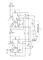
この実施の形態5では、チャージポンプ回路を3段以上接続する場合の構成例が示されている。その一例として、図5では、図1(実施の形態1)に示した構成において、3段目のチャージポンプ回路30が設けられ、選択信号発生回路12に代えて選択信号発生回路31が設けられている。そして、選択回路として、AND回路33,34,35が追加されている。
In the fifth embodiment, a configuration example in the case where three or more charge pump circuits are connected is shown. As an example, in FIG. 5, a third-stage
チャージポンプ回路30では、充電路を構成するスイッチ(PMOSトランジスタQ31,NMOSトランジスタQ32)と、放電路を構成するスイッチ(NMOSトランジスタQ330,331,332,PMOSトランジスタQ34)と、充電用コンデンサC31と、出力用コンデンサC32とを備えている。
In the
チャージポンプ回路30の充電側では、PMOSトランジスタQ31のソース電極は前段チャージポンプ回路11の出力電圧Vout2が印加され、PMOSトランジスタQ31のドレイン電極は、充電用コンデンサC31の一方の電極に接続されている。NMOSトランジスタQ32のドレイン電極は充電用コンデンサC31の他方の電極に接続され、NMOSトランジスタQ32のソース電極は、接地(グランド)に接続されている。そして、充電制御信号TC1が、NMOSトランジスタQ32のゲート電極に直接印加されるとともに、インバータQ53を介してPMOSトランジスタQ31のゲート電極に印加される。
On the charge side of the
チャージポンプ回路30の放電側では、NMOSトランジスタQ330,331,332は、ドレイン電極は共通に充電用コンデンサC31の他方の電極に接続されるが、NMOSトランジスタQ330のソース電極はチャージポンプ回路11の出力電圧Vout2が印加され、NMOSトランジスタQ331のソース電極は初段チャージポンプ回路10の出力電圧Vout1が印加され、NMOSトランジスタQ332のソース電極は入力電圧Vin0が印加されている。PMOSトランジスタQ34のソース電極は充電用コンデンサC31の一方の電極に接続され、PMOSトランジスタQ34のドレイン電極と接地との間には、出力用コンデンサC32が配置されている。
On the discharge side of the
そして、PMOSトランジスタQ34のゲート電極はインバータQ71が出力する放電制御信号TD1がインバータQ63を介して印加されるが、NMOSトランジスタQ330のソース電極はAND回路33の出力が印加され、NMOSトランジスタQ331のソース電極はAND回路34の出力が印加され、NMOSトランジスタQ332のソース電極はAND回路35の出力が印加されている。
The discharge control signal TD1 output from the inverter Q71 is applied to the gate electrode of the PMOS transistor Q34 via the inverter Q63. The output of the AND
選択信号発生回路31は、例えば図6に示すように構成され、入力電圧Vin0を入力電圧Viとして、5つの選択制御信号S1〜S5を発生するようになっている。選択制御信号S1〜S5はAND回路20,21,33〜35の各一方の入力端にそれぞれ印加される。AND回路33〜35の各他方の入力は、AND回路20,21と同様に、放電制御信号TD1が印加される。
The selection
図6は、図5に示す選択信号発生回路の構成例を示す回路図である。図6において、選択信号発生回路31は、入力電圧Viを並列にモニタする4個の抵抗分圧回路(R1,R2)(R3,R4)(R5,R6)(R7,R8)と、対応するモニタ電圧と対応する基準電圧Vrefとの大小関係を比較する4個の比較回路40,42,43,44と、比較回路40の出力を反転するインバータ41とを備えている。インバータ41の出力が選択制御信号S1となり、比較回路40,42,43,44の出力が、それぞれ選択制御信号S2,S3,S4,S5となるとしている。
FIG. 6 is a circuit diagram showing a configuration example of the selection signal generation circuit shown in FIG. In FIG. 6, the selection
次に、図5〜図7を参照して、以上のように構成される実施の形態5によるチャージポンプ方式電源回路の動作について説明する。なお、図7は、図5に示すチャージポンプ方式電源回路の昇圧動作を説明する図である。 Next, the operation of the charge pump power supply circuit according to the fifth embodiment configured as described above will be described with reference to FIGS. FIG. 7 is a diagram for explaining the boosting operation of the charge pump power supply circuit shown in FIG.
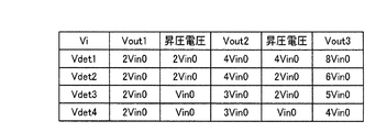
選択信号発生回路31の入力電圧Viは、入力電圧Vin0の検出電圧であり、図7に示すように、4種類の検出電圧Vdet1〜Vdet4からなる。ここで、検出電圧Vdet1〜Vdet4の大小関係は、Vdet1<Vdet2<Vdet3<Vdet4であるが、その電圧範囲は、選択制御信号S1〜S5のレベルが、次のような関係となるように定められている。
The input voltage Vi of the selection
すなわち、選択制御信号S1〜S5のレベルは、次のようになるとしている。入力電圧Vi=検出電圧Vdet1であるときは、S1=Hiレベル、S2=Loレベル、S3=Hiレベル、S4=S5=Loレベルとなる。入力電圧Vi=検出電圧Vdet2であるときは、S1=Hiレベル、S2=S3=Loレベル、S4=Hiレベル、S5=Loレベルとなる。入力電圧Vi=検出電圧Vdet3であるときは、S1=Loレベル、S2=Hiレベル、S3==Loレベル、S4=Hiレベル、S5=Loレベルとなる。入力電圧Vi=検出電圧Vdet4であるときは、S1=Loレベル、S2=Hiレベル、S3Loレベル、S4=Loレベル、S5=Hiレベルとなる。 That is, the levels of the selection control signals S1 to S5 are as follows. When the input voltage Vi = the detection voltage Vdet1, S1 = Hi level, S2 = Lo level, S3 = Hi level, and S4 = S5 = Lo level. When the input voltage Vi = the detection voltage Vdet2, S1 = Hi level, S2 = S3 = Lo level, S4 = Hi level, and S5 = Lo level. When the input voltage Vi = the detection voltage Vdet3, S1 = Lo level, S2 = Hi level, S3 == Lo level, S4 = Hi level, and S5 = Lo level. When the input voltage Vi = the detection voltage Vdet4, S1 = Lo level, S2 = Hi level, S3Lo level, S4 = Lo level, and S5 = Hi level.
放電制御信号TD1がHiレベルである放電期間でのチャージポンプ回路10の出力電圧Vout1は、4種類の検出電圧Vdet1〜Vdet4において、入力電圧Vin0の2倍に相当する2Vin0である。4種類の検出電圧Vdet1〜Vdet4におけるチャージポンプ回路11,30での昇圧動作は、次のようになる。
The output voltage Vout1 of the
(1)入力電圧Vi≧検出電圧Vdet1であるときは、AND回路20の出力はHiレベル、AND21の出力はLoレベル、AND回路33の出力はHiレベル、AND回路34,35の出力はそれぞれLoレベルである。チャージポンプ回路11ではNMOSトランジスタQ230がオン動作を行い、チャージポンプ回路30ではNMOSトランジスタ330がオン動作を行う。
(1) When the input voltage Vi ≧ the detection voltage Vdet1, the output of the AND
したがって、チャージポンプ回路11において充電用コンデンサC21の昇圧基礎電圧に加算する昇圧電圧は、2Vin0となるので、出力電圧Vout2に4Vin0なる電圧が得られる。この電圧4Vin0がチャージポンプ回路30において充電用コンデンサC21に充電される昇圧基礎電圧となるので、これに出力電圧Vout2=4Vin0が加算される。その結果、出力電圧Vout3に8Vin0なる電圧が得られる。
Therefore, since the boosted voltage added to the boosted basic voltage of the charging capacitor C21 in the
(2)入力電圧Vi≧検出電圧Vdet2であるときは、AND回路20の出力はHiレベル、AND回路21の出力はLoレベル、AND回路33の出力はLoレベル、AND回路34の出力はHiレベル、AND回路35の出力はLoレベルである。チャージポンプ回路11ではNMOSトランジスタQ230がオン動作を行い、チャージポンプ回路30ではNMOSトランジスタ331がオン動作を行う。
(2) When the input voltage Vi ≧ the detection voltage Vdet2, the output of the AND
したがって、チャージポンプ回路11において充電用コンデンサC21の昇圧基礎電圧に加算する昇圧電圧は、2Vin0となるので、出力電圧Vout2に4Vin0なる電圧が得られる。この電圧4Vin0がチャージポンプ回路30において充電用コンデンサC21に充電される昇圧基礎電圧となるので、これに出力電圧Vout1=2Vin0が加算される。その結果、出力電圧Vout3に6Vin0なる電圧が得られる。
Therefore, since the boosted voltage added to the boosted basic voltage of the charging capacitor C21 in the
(3)入力電圧Vi≧検出電圧Vdet3であるときは、AND回路20の出力はLoレベル、AND回路21の出力はHiレベル、AND回路33の出力はLoレベル、AND回路34の出力はHiレベル、AND回路35の出力はLoレベルである。チャージポンプ回路11ではNMOSトランジスタQ231がオン動作を行い、チャージポンプ回路30ではNMOSトランジスタ331がオン動作を行う。
(3) When the input voltage Vi ≧ the detection voltage Vdet3, the output of the AND
したがって、チャージポンプ回路11において充電用コンデンサC21の昇圧基礎電圧に加算する昇圧電圧は、入力電圧Vin0となるので、出力電圧Vout2に3Vin0なる電圧が得られる。この電圧3Vin0がチャージポンプ回路30において充電用コンデンサC21に充電される昇圧基礎電圧となるので、これに出力電圧Vout1=2Vin0が加算される。その結果、出力電圧Vout3に5Vin0なる電圧が得られる。
Therefore, since the boosted voltage added to the boosted basic voltage of the charging capacitor C21 in the
(4)入力電圧Vi≧検出電圧Vdet4であるときは、AND回路20の出力はLoレベル、AND回路21の出力はHiレベル、AND回路33の出力はLoレベル、AND回路34の出力はLoレベル、AND回路35の出力はHiレベルである。チャージポンプ回路11ではNMOSトランジスタQ231がオン動作を行い、チャージポンプ回路30ではNMOSトランジスタ332がオン動作を行う。
(4) When the input voltage Vi ≧ the detection voltage Vdet4, the output of the AND
したがって、チャージポンプ回路11において充電用コンデンサC21の昇圧基礎電圧に加算する昇圧電圧は、入力電圧Vin0となるので、出力電圧Vout2に3Vin0なる電圧が得られる。この電圧3Vin0がチャージポンプ回路30において充電用コンデンサC21に充電される昇圧基礎電圧となるので、これに入力電圧Vin0が加算される。その結果、出力電圧Vout3に4Vin0なる電圧が得られる。
Therefore, since the boosted voltage added to the boosted basic voltage of the charging capacitor C21 in the
このように、実施の形態5によれば、2段目のチャージポンプ回路が入力電圧Vin0の3倍と4倍との昇圧が行える場合に、3段目のチャージポンプ回路にて昇圧に用いる電圧を、入力電圧Vin0と初段チャージポンプ回路の出力電圧Vout1と2段目チャージポンプ回路の出力電圧Vout2との3つから選択できるようにしたので、3段目のチャージポンプ回路の出力には、入力電圧Vin0の4倍〜8倍の電圧が得られる。
As described above, according to the fifth embodiment, when the second-stage charge pump circuit can boost the input voltage Vin0 by 3 and 4 times, the voltage used for boosting by the third-stage charge pump circuit. Can be selected from among the input voltage Vin0, the output voltage Vout1 of the first stage charge pump circuit, and the output voltage Vout2 of the second stage charge pump circuit. A
なお、この実施の形態5では、実施の形態1への適用例を示したが、実施の形態2〜3にも同様に適用することができる。このとき、2段目と3段目において、双方が充電側または放電側で切り替えを行うようにしてもよいが、一方が充電側で切り替えを行い、他方が放電側で切り替えを行うようにしてもよい。 In the fifth embodiment, the application example to the first embodiment is shown. However, the fifth embodiment can be similarly applied to the second to third embodiments. At this time, in the second stage and the third stage, both may be switched on the charge side or the discharge side, but one is switched on the charge side and the other is switched on the discharge side. Also good.
また、実施の形態5の説明から理解できるように、多段に接続するチャージポンプ回路は、4段以上であっても同様の考えで構成できることは言うまでもない。 Further, as can be understood from the description of the fifth embodiment, it is needless to say that charge pump circuits connected in multiple stages can be configured with the same idea even if there are four or more stages.
さらに、実施の形態1〜5では、選択信号発生回路では、選択制御信号を作るのに比較回路を用いたが、ヒステリシス特性を持つようにしてもよい。また、電圧を検知できる回路であればよいので、その種類は問わない。 Furthermore, in the first to fifth embodiments, the selection signal generation circuit uses the comparison circuit to generate the selection control signal, but may have a hysteresis characteristic. Further, any circuit can be used as long as it can detect a voltage.
以上のように、この発明にかかるチャージポンプ方式電源回路は、入力電圧を安定化させることなく直接印加することができ、かつ入力電圧の変更に対して素子耐圧を問題にすることなく高電圧を取得するのに有用である。 As described above, the charge pump power supply circuit according to the present invention can directly apply the input voltage without stabilizing it, and can apply a high voltage to the change of the input voltage without causing a problem with the element breakdown voltage. Useful to get.
10,11,25,30 チャージポンプ回路(チャージポンプ方式電源回路)
12,31 選択信号発生回路
15,40,42〜44 比較回路
16,41 インバータ
20,21,33〜35 選択回路を構成するAND回路
R1〜R8 入力電圧をモニタする抵抗分圧回路を構成する抵抗素子
Vref 基準電圧源の電圧
Q11,Q14,Q21,Q24,Q210,Q211,Q31,Q34 PMOSトランジスタ
Q12,Q13,Q22,Q230,Q231,Q23,Q32,Q330〜Q332 NMOSトランジスタ
C11,C21,C31 充電用コンデンサ
C11,C21,C31 出力用コンデンサ
Q51,Q61,Q52,Q62,Q53,Q63,Q71 インバータ
Vin0 入力電源の電圧
Vout1 初段チャージポンプ回路の出力電圧
Vout2 2段目チャージポンプ回路の出力電圧
Vout3 3段目チャージポンプ回路の出力電圧
TC1 充電制御信号
TD1 放電制御信号
10, 11, 25, 30 Charge pump circuit (charge pump type power supply circuit)
12, 31 Selection
Claims (9)
2段目のチャージポンプ回路は、前記2つの昇圧用スイッチのうち前記コンデンサの充電電圧に昇圧電圧を加算する側に設けられる昇圧用スイッチが各一端を共通に前記コンデンサに接続され、各他端に互いに異なる値の昇圧電圧が印加される複数のスイッチで構成され、
昇圧動作期間において初段チャージポンプ回路の入力電圧または前記初段チャージポンプ回路からの入力電圧の値に応じて前記複数のスイッチの一つを選択して閉路動作させる手段、
を備えることを特徴とするチャージポンプ方式電源回路。 A charge pump circuit comprising two charging switches that perform an operation of charging a capacitor to an input voltage and two boosting switches that perform an operation of adding the input voltage to the charging voltage of the capacitor to increase the voltage in two stages. A charge pump type power supply circuit connected longitudinally,
In the second stage charge pump circuit, one of the two boosting switches provided on the side of adding the boosted voltage to the charging voltage of the capacitor is connected to the capacitor in common at one end, and the other end Is composed of a plurality of switches to which boosted voltages of different values are applied,
Means for selecting one of the plurality of switches according to a value of an input voltage of the first stage charge pump circuit or an input voltage from the first stage charge pump circuit in a boosting operation period, and performing a closing operation;
A charge pump type power supply circuit comprising:
2段目のチャージポンプ回路は、前記2つの充電用スイッチのうち前記コンデンサに充電を行う高電位側に設けられる充電用スイッチが各一端を共通に前記コンデンサに接続され、各他端に互いに異なる値の充電用電圧が印加される複数のスイッチで構成され、
充電動作期間において初段チャージポンプ回路の入力電圧または前記初段チャージポンプ回路からの入力電圧の値に応じて前記複数のスイッチの一つを選択して閉路動作させる手段、
を備えることを特徴とするチャージポンプ方式電源回路。 A charge pump circuit comprising two charging switches that perform an operation of charging a capacitor to an input voltage and two boosting switches that perform an operation of adding the input voltage to the charging voltage of the capacitor to increase the voltage in two stages. A charge pump type power supply circuit connected longitudinally,
In the second-stage charge pump circuit, a charge switch provided on the high potential side for charging the capacitor among the two charge switches is connected to the capacitor at one end in common and is different from each other at the other end. Consists of a plurality of switches to which value charging voltage is applied,
Means for selecting one of the plurality of switches according to the input voltage of the first stage charge pump circuit or the value of the input voltage from the first stage charge pump circuit during the charging operation period,
A charge pump type power supply circuit comprising:
2段目と3段目のチャージポンプ回路は、それぞれ、
前記2つの昇圧用スイッチのうち前記コンデンサの充電電圧に昇圧電圧を加算する側に設けられる昇圧用スイッチが各一端を共通に前記コンデンサに接続され、各他端に互いに異なる値の昇圧電圧が印加される複数のスイッチで構成され、または、前記2つの充電用スイッチのうち前記コンデンサに充電を行う高電位側に設けられる充電用スイッチが各一端を共通に前記コンデンサに接続され、各他端に互いに異なる値の充電用電圧が印加される複数のスイッチで構成され、
昇圧動作期間と充電期間の該当する期間において初段チャージポンプ回路の入力電圧または前記初段チャージポンプ回路からの入力電圧の値に応じて前記2段目と3段目のチャージポンプ回路における複数のスイッチの一つをそれぞれ選択して閉路動作させる手段、
を備えることを特徴とするチャージポンプ方式電源回路。 A charge pump circuit comprising two charging switches that perform an operation of charging a capacitor to an input voltage and two boosting switches that perform an operation of adding the input voltage to the charging voltage of the capacitor to boost the voltage in three stages. A charge pump type power supply circuit connected longitudinally,
The second and third stage charge pump circuits are respectively
A boosting switch provided on the side of adding the boosted voltage to the charging voltage of the capacitor among the two boosting switches is connected to the capacitor at one end in common, and boosted voltages having different values are applied to the other ends. Or a charging switch provided on the high potential side for charging the capacitor among the two charging switches is connected to the capacitor in common at one end and connected to the other end. Consists of a plurality of switches to which charging voltages of different values are applied,
Depending on the value of the input voltage of the first stage charge pump circuit or the input voltage from the first stage charge pump circuit in the corresponding period of the boosting operation period and the charging period, a plurality of switches in the second stage and third stage charge pump circuits are connected. Means for selecting and closing each one,
A charge pump type power supply circuit comprising:
前記2段目のチャージポンプ回路における前記互いに異なる値の昇圧電圧または充電用電圧は、初段チャージポンプ回路の入力電圧と、前記初段チャージポンプ回路の出力電圧とで構成され、
前記3段目のチャージポンプ回路における前記互いに異なる値の昇圧電圧または充電用電圧は、初段チャージポンプ回路の入力電圧と前記初段チャージポンプ回路の出力電圧と前記2段目チャージポンプ回路の出力電圧とで構成される、
ことを特徴とする請求項5に記載のチャージポンプ方式電源回路。 When the plurality of switches in the second-stage charge pump circuit are two and the plurality of switches in the third-stage charge pump circuit are three,
The boosted voltage or charging voltage having different values in the second stage charge pump circuit is composed of an input voltage of the first stage charge pump circuit and an output voltage of the first stage charge pump circuit,
The boosted voltage or charging voltage having different values in the third-stage charge pump circuit includes an input voltage of the first-stage charge pump circuit, an output voltage of the first-stage charge pump circuit, and an output voltage of the second-stage charge pump circuit. Composed of,
The charge pump type power supply circuit according to claim 5.
2段以降の各チャージポンプ回路は、前記2つの昇圧用スイッチのうち前記コンデンサの充電電圧に昇圧電圧を加算する側に設けられる昇圧用スイッチが各一端を共通に前記コンデンサに接続され、各他端に互いに異なる値の昇圧電圧が印加される複数のスイッチで構成され、
昇圧動作期間において、少なくとも初段チャージポンプ回路の入力電圧または前記初段チャージポンプ回路からの入力電圧の値に応じて前記複数のスイッチの一つを選択して閉路動作させる手段、
を備えることを特徴とするチャージポンプ方式電源回路。 A charge pump circuit including two charging switches that perform an operation of charging a capacitor up to an input voltage and two boosting switches that perform an operation of adding the input voltage to the charging voltage of the capacitor to increase the voltage is vertically arranged in multiple stages. A charge pump type power supply circuit,
In each of the charge pump circuits in the second and subsequent stages, a booster switch provided on the side of adding the boosted voltage to the charging voltage of the capacitor among the two booster switches is connected to the capacitor in common at one end. It is composed of a plurality of switches to which boosted voltages of different values are applied to the ends,
Means for selecting one of the plurality of switches according to a value of at least an input voltage of the first stage charge pump circuit or an input voltage from the first stage charge pump circuit and performing a closing operation in the boosting operation period;
A charge pump type power supply circuit comprising:
2段以降の各チャージポンプ回路は、前記2つの充電用スイッチのうち前記コンデンサに充電を行う高電位側に設けられる充電用スイッチが各一端を共通に前記コンデンサに接続され、各他端に互いに異なる値の充電用電圧が印加される複数のスイッチで構成され、
充電動作期間において、少なくとも初段チャージポンプ回路の入力電圧または前記初段チャージポンプ回路からの入力電圧の値に応じて前記複数のスイッチの一つを選択して閉路動作させる手段、
を備えることを特徴とするチャージポンプ方式電源回路。 A charge pump circuit including two charging switches that perform an operation of charging a capacitor up to an input voltage and two boosting switches that perform an operation of adding the input voltage to the charging voltage of the capacitor to increase the voltage is vertically arranged in multiple stages. A charge pump type power supply circuit,
In each of the charge pump circuits in the second and subsequent stages, a charge switch provided on the high potential side for charging the capacitor among the two charge switches is connected to the capacitor in common at one end, and is connected to the other end at each other. Consists of a plurality of switches to which charging voltages of different values are applied,
Means for selecting one of the plurality of switches according to a value of at least an input voltage of the first stage charge pump circuit or an input voltage from the first stage charge pump circuit during a charging operation period;
A charge pump type power supply circuit comprising:
2段以降の各チャージポンプ回路は、
前記2つの昇圧用スイッチのうち前記コンデンサの充電電圧に昇圧電圧を加算する側に設けられる昇圧用スイッチが各一端を共通に前記コンデンサに接続され、各他端に互いに異なる値の昇圧電圧が印加される複数のスイッチと、前記2つの充電用スイッチのうち前記コンデンサに充電を行う高電位側に設けられる充電用スイッチが各一端を共通に前記コンデンサに接続され、各他端に互いに異なる値の充電用電圧が印加される複数のスイッチとが混在して構成され、
昇圧動作期間と充電期間の該当する期間において、少なくとも初段チャージポンプ回路の入力電圧または前記初段チャージポンプ回路からの入力電圧の値に応じて前記複数のスイッチの一つを選択して閉路動作させる手段、
を備えることを特徴とするチャージポンプ方式電源回路。
A charge pump circuit including two charging switches that perform an operation of charging a capacitor up to an input voltage and two boosting switches that perform an operation of adding the input voltage to the charging voltage of the capacitor to increase the voltage is vertically arranged in multiple stages. A charge pump type power supply circuit,
Each charge pump circuit after the second stage is
A boosting switch provided on the side of adding the boosted voltage to the charging voltage of the capacitor among the two boosting switches is connected to the capacitor at one end in common, and boosted voltages having different values are applied to the other ends. A plurality of switches, and a charging switch provided on a high potential side for charging the capacitor among the two charging switches, one end of which is commonly connected to the capacitor, and each of the other ends has a different value. It consists of multiple switches to which charging voltage is applied,
Means for selecting and closing one of the plurality of switches in accordance with at least the input voltage of the first stage charge pump circuit or the input voltage from the first stage charge pump circuit in the corresponding period of the boosting operation period and the charging period ,
A charge pump type power supply circuit comprising:
Priority Applications (2)
| Application Number | Priority Date | Filing Date | Title |
|---|---|---|---|
| JP2004347520A JP2006158132A (en) | 2004-11-30 | 2004-11-30 | Charge-pump power supply circuit |
| US11/268,484 US20060114053A1 (en) | 2004-11-30 | 2005-11-08 | Charge-pump-type power supply circuit |
Applications Claiming Priority (1)
| Application Number | Priority Date | Filing Date | Title |
|---|---|---|---|
| JP2004347520A JP2006158132A (en) | 2004-11-30 | 2004-11-30 | Charge-pump power supply circuit |
Publications (1)
| Publication Number | Publication Date |
|---|---|
| JP2006158132A true JP2006158132A (en) | 2006-06-15 |
Family
ID=36566807
Family Applications (1)
| Application Number | Title | Priority Date | Filing Date |
|---|---|---|---|
| JP2004347520A Pending JP2006158132A (en) | 2004-11-30 | 2004-11-30 | Charge-pump power supply circuit |
Country Status (2)
| Country | Link |
|---|---|
| US (1) | US20060114053A1 (en) |
| JP (1) | JP2006158132A (en) |
Cited By (4)
| Publication number | Priority date | Publication date | Assignee | Title |
|---|---|---|---|---|
| JP2008125145A (en) * | 2006-11-08 | 2008-05-29 | Mcm Japan Kk | Voltage step-up circuit and voltage step-down circuit |
| JP2008193766A (en) * | 2007-02-01 | 2008-08-21 | Spansion Llc | Voltage generating circuit and control method thereof |
| JP2008199745A (en) * | 2007-02-09 | 2008-08-28 | Matsushita Electric Works Ltd | Power supply circuit |
| JP2014187764A (en) * | 2013-03-22 | 2014-10-02 | Toshiba Corp | Voltage conversion circuit and switching control circuit |
Families Citing this family (45)
| Publication number | Priority date | Publication date | Assignee | Title |
|---|---|---|---|---|
| JP2005348561A (en) * | 2004-06-04 | 2005-12-15 | Renesas Technology Corp | Charge pump power supply circuit |
| US7724603B2 (en) * | 2007-08-03 | 2010-05-25 | Freescale Semiconductor, Inc. | Method and circuit for preventing high voltage memory disturb |
| US8044705B2 (en) * | 2007-08-28 | 2011-10-25 | Sandisk Technologies Inc. | Bottom plate regulation of charge pumps |
| US7586362B2 (en) * | 2007-12-12 | 2009-09-08 | Sandisk Corporation | Low voltage charge pump with regulation |
| US7586363B2 (en) * | 2007-12-12 | 2009-09-08 | Sandisk Corporation | Diode connected regulation of charge pumps |
| US7839689B2 (en) | 2008-01-31 | 2010-11-23 | Mosaid Technologies Incorporated | Power supplies in flash memory devices and systems |
| US20090302930A1 (en) * | 2008-06-09 | 2009-12-10 | Feng Pan | Charge Pump with Vt Cancellation Through Parallel Structure |
| US7969235B2 (en) | 2008-06-09 | 2011-06-28 | Sandisk Corporation | Self-adaptive multi-stage charge pump |
| US8710907B2 (en) | 2008-06-24 | 2014-04-29 | Sandisk Technologies Inc. | Clock generator circuit for a charge pump |
| US7683700B2 (en) * | 2008-06-25 | 2010-03-23 | Sandisk Corporation | Techniques of ripple reduction for charge pumps |
| US7956673B2 (en) * | 2008-08-11 | 2011-06-07 | Micron Technology, Inc. | Variable stage charge pump and method for providing boosted output voltage |
| US7795952B2 (en) * | 2008-12-17 | 2010-09-14 | Sandisk Corporation | Regulation of recovery rates in charge pumps |
| EP2244364A1 (en) * | 2009-04-23 | 2010-10-27 | Mitsubishi Electric R&D Centre Europe B.V. | Method and an apparatus for controlling the switches of a boost converter composed of plural bridge devices |
| TWI397248B (en) * | 2009-06-22 | 2013-05-21 | Richtek Technology Corp | Multi-input charge pump, and control circuit and operation method thereof |
| US7973592B2 (en) * | 2009-07-21 | 2011-07-05 | Sandisk Corporation | Charge pump with current based regulation |
| US8339183B2 (en) * | 2009-07-24 | 2012-12-25 | Sandisk Technologies Inc. | Charge pump with reduced energy consumption through charge sharing and clock boosting suitable for high voltage word line in flash memories |
| US8013666B1 (en) * | 2009-07-31 | 2011-09-06 | Altera Corporation | Low ripple charge pump |
| US20110148509A1 (en) * | 2009-12-17 | 2011-06-23 | Feng Pan | Techniques to Reduce Charge Pump Overshoot |
| US8294509B2 (en) | 2010-12-20 | 2012-10-23 | Sandisk Technologies Inc. | Charge pump systems with reduction in inefficiencies due to charge sharing between capacitances |
| US8339185B2 (en) | 2010-12-20 | 2012-12-25 | Sandisk 3D Llc | Charge pump system that dynamically selects number of active stages |
| KR20120078857A (en) * | 2011-01-03 | 2012-07-11 | 에스케이하이닉스 주식회사 | Method and apparatus for generating voltage |
| US8699247B2 (en) | 2011-09-09 | 2014-04-15 | Sandisk Technologies Inc. | Charge pump system dynamically reconfigurable for read and program |
| US8514628B2 (en) | 2011-09-22 | 2013-08-20 | Sandisk Technologies Inc. | Dynamic switching approach to reduce area and power consumption of high voltage charge pumps |
| US8400212B1 (en) | 2011-09-22 | 2013-03-19 | Sandisk Technologies Inc. | High voltage charge pump regulation system with fine step adjustment |
| CN102629822B (en) * | 2012-03-30 | 2014-09-03 | 格科微电子(上海)有限公司 | Charge pump and liquid crystal display screen driving chip |
| US8710909B2 (en) | 2012-09-14 | 2014-04-29 | Sandisk Technologies Inc. | Circuits for prevention of reverse leakage in Vth-cancellation charge pumps |
| US8836412B2 (en) | 2013-02-11 | 2014-09-16 | Sandisk 3D Llc | Charge pump with a power-controlled clock buffer to reduce power consumption and output voltage ripple |
| CN103178709B (en) * | 2013-02-27 | 2015-12-16 | 格科微电子(上海)有限公司 | Charge pump circuit and sequential control method thereof |
| US8981835B2 (en) | 2013-06-18 | 2015-03-17 | Sandisk Technologies Inc. | Efficient voltage doubler |
| US9024680B2 (en) | 2013-06-24 | 2015-05-05 | Sandisk Technologies Inc. | Efficiency for charge pumps with low supply voltages |
| US9077238B2 (en) | 2013-06-25 | 2015-07-07 | SanDisk Technologies, Inc. | Capacitive regulation of charge pumps without refresh operation interruption |
| US9007046B2 (en) | 2013-06-27 | 2015-04-14 | Sandisk Technologies Inc. | Efficient high voltage bias regulation circuit |
| US8896367B1 (en) * | 2013-07-18 | 2014-11-25 | Ememory Technology Inc. | Charge pump system |
| US9083231B2 (en) | 2013-09-30 | 2015-07-14 | Sandisk Technologies Inc. | Amplitude modulation for pass gate to improve charge pump efficiency |
| US9154027B2 (en) | 2013-12-09 | 2015-10-06 | Sandisk Technologies Inc. | Dynamic load matching charge pump for reduced current consumption |
| CN104410271B (en) * | 2014-12-17 | 2017-10-10 | 南京航空航天大学 | A kind of five conversion specific charge pump multiphase deinterleaving methods realized with three striding capacitances |
| US9917507B2 (en) | 2015-05-28 | 2018-03-13 | Sandisk Technologies Llc | Dynamic clock period modulation scheme for variable charge pump load currents |
| US9647536B2 (en) | 2015-07-28 | 2017-05-09 | Sandisk Technologies Llc | High voltage generation using low voltage devices |
| US9520776B1 (en) | 2015-09-18 | 2016-12-13 | Sandisk Technologies Llc | Selective body bias for charge pump transfer switches |
| JP6632865B2 (en) * | 2015-10-29 | 2020-01-22 | シナプティクス・ジャパン合同会社 | Semiconductor device having booster and booster circuit |
| US20170279349A1 (en) * | 2016-03-24 | 2017-09-28 | Linear Technology Corporation | High efficiency charge pump with auxiliary input operative to optimize conversion ratio |
| CN106849645A (en) * | 2016-08-15 | 2017-06-13 | 珠海市魅族科技有限公司 | A kind of charging circuit, method and electronic installation |
| CN106655762B (en) * | 2017-01-11 | 2019-06-18 | 南京矽力杰半导体技术有限公司 | Isolated form Switching capacitors |
| US10193541B1 (en) * | 2017-09-13 | 2019-01-29 | Siemens Medical Solutions Usa, Inc. | Transformerless switching regulator with controllable boost factor |
| CN111865075B (en) * | 2020-07-27 | 2021-11-05 | 合肥工业大学 | Boost conversion circuit suitable for light energy collection structure |
Family Cites Families (8)
| Publication number | Priority date | Publication date | Assignee | Title |
|---|---|---|---|---|
| JPH05268763A (en) * | 1992-03-17 | 1993-10-15 | Nec Corp | Dc/dc converter circuit and rs-232 interface circuit employing same |
| US5859632A (en) * | 1994-07-14 | 1999-01-12 | Seiko Epson Corporation | Power circuit, liquid crystal display device and electronic equipment |
| KR100275743B1 (en) * | 1998-09-08 | 2001-01-15 | 윤종용 | Boosting circuit and boosting method thereof |
| DE10050496B4 (en) * | 2000-10-11 | 2015-04-02 | Texas Instruments Deutschland Gmbh | DC converter |
| US6861894B2 (en) * | 2002-09-27 | 2005-03-01 | Sandisk Corporation | Charge pump with Fibonacci number multiplication |
| JP3697695B2 (en) * | 2003-01-23 | 2005-09-21 | 日本テキサス・インスツルメンツ株式会社 | Charge pump type DC / DC converter |
| JP2005348561A (en) * | 2004-06-04 | 2005-12-15 | Renesas Technology Corp | Charge pump power supply circuit |
| JP4379416B2 (en) * | 2005-04-26 | 2009-12-09 | エプソンイメージングデバイス株式会社 | LED drive circuit, illumination device, and electro-optical device |
-
2004
- 2004-11-30 JP JP2004347520A patent/JP2006158132A/en active Pending
-
2005
- 2005-11-08 US US11/268,484 patent/US20060114053A1/en not_active Abandoned
Cited By (5)
| Publication number | Priority date | Publication date | Assignee | Title |
|---|---|---|---|---|
| JP2008125145A (en) * | 2006-11-08 | 2008-05-29 | Mcm Japan Kk | Voltage step-up circuit and voltage step-down circuit |
| JP2008193766A (en) * | 2007-02-01 | 2008-08-21 | Spansion Llc | Voltage generating circuit and control method thereof |
| JP2008199745A (en) * | 2007-02-09 | 2008-08-28 | Matsushita Electric Works Ltd | Power supply circuit |
| JP2014187764A (en) * | 2013-03-22 | 2014-10-02 | Toshiba Corp | Voltage conversion circuit and switching control circuit |
| US9350233B2 (en) | 2013-03-22 | 2016-05-24 | Kabushiki Kaisha Toshiba | Voltage conversion circuit and switching control circuit |
Also Published As
| Publication number | Publication date |
|---|---|
| US20060114053A1 (en) | 2006-06-01 |
Similar Documents
| Publication | Publication Date | Title |
|---|---|---|
| JP2006158132A (en) | Charge-pump power supply circuit | |
| JP5063299B2 (en) | Method for controlling operation of charge pump circuit | |
| US7808302B2 (en) | Type of charge pump apparatus and power source circuit | |
| US20110133821A1 (en) | Charge pump circuit | |
| US20070159233A1 (en) | Charge pump power supply circuit | |
| US11671015B2 (en) | Three-level boost circuit and multiple-output parallel system | |
| JP2003033007A (en) | Controlling method for charge pump circuit | |
| TW202119744A (en) | Multi-level converter with voltage divider for pre-charging flying capacitor | |
| JP2010119226A (en) | Charge pump circuit | |
| US20160241218A1 (en) | Semiconductor device | |
| US7365592B2 (en) | Power supply circuit | |
| JP6205596B2 (en) | Soft start circuit and power supply device | |
| US6556066B2 (en) | Boosting method and apparatus | |
| JP2008099481A (en) | Charge pump circuit | |
| JP2018098901A (en) | Charge pump circuit and boosting circuit | |
| US20160026200A1 (en) | Power supply circuit | |
| WO2018083851A1 (en) | Voltage detection device | |
| US7969232B2 (en) | Booster and voltage detection method thereof | |
| JP2005057969A (en) | Charge-pump circuit | |
| JP2010104140A (en) | Power supply circuit | |
| JP2022112806A (en) | Power supply control device | |
| JP2005117830A (en) | Charge pump circuit | |
| EP1677308A1 (en) | Low-ripple boosted voltage generator | |
| JP2020028172A (en) | Power supply circuit | |
| US20180166986A1 (en) | Charge pump circuit |