JP2011507463A - Circuit for controlling the current flowing through the electric control member or the voltage between the terminals of the electric control member - Google Patents
Circuit for controlling the current flowing through the electric control member or the voltage between the terminals of the electric control member Download PDFInfo
- Publication number
- JP2011507463A JP2011507463A JP2010536504A JP2010536504A JP2011507463A JP 2011507463 A JP2011507463 A JP 2011507463A JP 2010536504 A JP2010536504 A JP 2010536504A JP 2010536504 A JP2010536504 A JP 2010536504A JP 2011507463 A JP2011507463 A JP 2011507463A
- Authority
- JP
- Japan
- Prior art keywords
- state
- duty cycle
- switch
- voltage
- switches
- Prior art date
- Legal status (The legal status is an assumption and is not a legal conclusion. Google has not performed a legal analysis and makes no representation as to the accuracy of the status listed.)
- Pending
Links
Images


Classifications
-
- H—ELECTRICITY
- H02—GENERATION; CONVERSION OR DISTRIBUTION OF ELECTRIC POWER
- H02M—APPARATUS FOR CONVERSION BETWEEN AC AND AC, BETWEEN AC AND DC, OR BETWEEN DC AND DC, AND FOR USE WITH MAINS OR SIMILAR POWER SUPPLY SYSTEMS; CONVERSION OF DC OR AC INPUT POWER INTO SURGE OUTPUT POWER; CONTROL OR REGULATION THEREOF
- H02M7/00—Conversion of ac power input into dc power output; Conversion of dc power input into ac power output
- H02M7/42—Conversion of dc power input into ac power output without possibility of reversal
- H02M7/44—Conversion of dc power input into ac power output without possibility of reversal by static converters
- H02M7/48—Conversion of dc power input into ac power output without possibility of reversal by static converters using discharge tubes with control electrode or semiconductor devices with control electrode
- H02M7/53—Conversion of dc power input into ac power output without possibility of reversal by static converters using discharge tubes with control electrode or semiconductor devices with control electrode using devices of a triode or transistor type requiring continuous application of a control signal
- H02M7/537—Conversion of dc power input into ac power output without possibility of reversal by static converters using discharge tubes with control electrode or semiconductor devices with control electrode using devices of a triode or transistor type requiring continuous application of a control signal using semiconductor devices only, e.g. single switched pulse inverters
- H02M7/5387—Conversion of dc power input into ac power output without possibility of reversal by static converters using discharge tubes with control electrode or semiconductor devices with control electrode using devices of a triode or transistor type requiring continuous application of a control signal using semiconductor devices only, e.g. single switched pulse inverters in a bridge configuration
- H02M7/53871—Conversion of dc power input into ac power output without possibility of reversal by static converters using discharge tubes with control electrode or semiconductor devices with control electrode using devices of a triode or transistor type requiring continuous application of a control signal using semiconductor devices only, e.g. single switched pulse inverters in a bridge configuration with automatic control of output voltage or current
Landscapes
- Engineering & Computer Science (AREA)
- Power Engineering (AREA)
- Control Of Direct Current Motors (AREA)
- Inverter Devices (AREA)
- Control Of Ac Motors In General (AREA)
Abstract
【課題】 電気制御部材における電流及び制御部材の端子間の電圧を制御する回路を提供する。
【解決手段】 電気制御部材(110)において電流を制御するための回路300であって、電気制御部材(110)は、4つの端子(105,106,107,108)備えるブリッジと、4つの制御スイッチ(AH,AL,BH,BL)と、電源(109)と、4つのスイッチのうち少なくとも2つのスイッチに対するPWM制御手段とを備えている。制御回路は、第1のスイッチ(AH)及び第4のスイッチ(BL)は閉じており、第2のスイッチ(BH)及び第3のスイッチ(AL)は開いている第1の状態、第2のスイッチ(BH)及び第3のスイッチ(AL)は閉じており、第1のスイッチ(AH)及び第4のスイッチ(BL)は開いている第2の状態、及び次の2つの状態のうち少なくとも1つの状態であることを示す。すなわち、第3のスイッチ(AL)及び第4のスイッチ(BL)は閉じており、第1のスイッチ(AH)及び第2のスイッチ(BH)は開いている第3の状態、及び/又は第1のスイッチ(AH)及び第2のスイッチ(BH)は閉じており、第3のスイッチ(AL)及び第4のスイッチ(BL)は開いている第4の状態とである。
【選択図】図8PROBLEM TO BE SOLVED: To provide a circuit for controlling a current in an electric control member and a voltage between terminals of the control member.
A circuit 300 for controlling an electric current in an electric control member (110), the electric control member (110) including a bridge having four terminals (105, 106, 107, 108) and four controls. A switch (AH, AL, BH, BL), a power source (109), and PWM control means for at least two of the four switches are provided. In the control circuit, the first switch (AH) and the fourth switch (BL) are closed, the second switch (BH) and the third switch (AL) are opened, and the second state The switch (BH) and the third switch (AL) are closed, the first switch (AH) and the fourth switch (BL) are in the open second state, and the following two states: Indicates at least one state. That is, the third switch (AL) and the fourth switch (BL) are closed, the first switch (AH) and the second switch (BH) are in the open third state, and / or The first switch (AH) and the second switch (BH) are closed, and the third switch (AL) and the fourth switch (BL) are in the open fourth state.
[Selection] Figure 8
Description
本発明は、電気制御部材を流れる電流又は電気制御部材の端子間の電圧を制御する回路に関する。本発明の特に好ましい用途は、自動車におけるいわゆる電磁気バルブ(“カム無し”システム)に使用されるアクチュエータのような可変インダクタンスを伴う電流又は電気機械を制御する分野にある。 The present invention relates to a circuit for controlling a current flowing through an electric control member or a voltage between terminals of the electric control member. A particularly preferred application of the invention is in the field of controlling currents or electrical machines with variable inductance, such as actuators used in so-called electromagnetic valves (“camless” systems) in automobiles.
バルブの電磁気的作動には、電気エネルギーが必要である。この電気エネルギーは、車に搭載の回路から取り出される。電磁気バルブシステムの性能は、車載回路の電気エネルギー消費の最小化に関係する。実際には、クランクシャフトの出力部において使用可能なパワーは、ヒートエンジンによって生み出される全パワーから、補助装置の正確な動作(バルブの動作、水及びオイルポンプの駆動、その他)に対して必要なパワーを減じたものに等しい。 Electrical energy is required for electromagnetic operation of the valve. This electrical energy is taken from a circuit mounted on the car. The performance of the electromagnetic valve system is related to minimizing the electrical energy consumption of the on-board circuit. In practice, the power available at the output of the crankshaft is required for the correct operation of the auxiliary equipment (valve operation, water and oil pump drive, etc.) from the total power produced by the heat engine. Equivalent to reduced power.
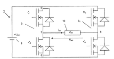
一般に、正又は負の電流制御電気機械は、頻繁にH型パワーブリッジによって制御されることが多く、機械の構造により単相又は多相である“フォー・クオドラント“ ブリッジ(又は、“フル・ブリッジ チョッパー”)とも呼ばれている。“フォー・クオドラント“ ブリッジという語は、電圧−電流特性の全ての象限において機能するブリッジ制御を意味するものとされている。一般に、制御電子機器は、パワーブリッジへ固定周波数を伴うPWM(パルス幅変調)型制御を適用することにより、電流を設定値とする。“フォー・クオドラント“ ブリッジ1の電子構造の一例を、図1に示してある。ブリッジ1は、次の要素を備えている。
− 4端子5,6,7及び8、
− ブリッジ1の第1及び第2端子5及び6に接続されたDC電源9(これは、例えば、バッテリー、DC−DCパワーコンバータ、又はAC−DCパワーコンバータである)、
− アクチュエータを制御するために用いられ、ブリッジ回路1の第3及び第4の端子7及び8の間に接続されている(可変インダクタンスによる電気的負荷のような)電子制御部材10、
− 第1及び第3の端子5及び7の間に接続されている第1スイッチC1、
− 第1及び第4の端子5及び8の間に接続されている第2スイッチC2、
− 第2及び第3の端子6及び7の間に接続されている第3スイッチC3、
− 第2及び第4の端子6及び8の間に接続される第4スイッチC4。
In general, positive or negative current controlled electric machines are often controlled by H-type power bridges and are “four quadrant” bridges (or “full bridges”) that are single or multiphase depending on the machine structure. Also called “chopper”). The term “four quadrant” bridge is intended to mean a bridge control that functions in all quadrants of the voltage-current characteristic. In general, the control electronics sets the current as a set value by applying PWM (pulse width modulation) type control with a fixed frequency to the power bridge. An example of the electronic structure of the “four quadrant”
-4
A
An electronic control member 10 (such as an electrical load with variable inductance) used to control the actuator and connected between the third and
A first switch C 1 connected between the first and
A second switch C 2 connected between the first and
A third switch C 3 connected between the second and
A fourth switch C 4 connected between the second and
従って、ブリッジ1は、直列のスイッチC1及びC3、直列のスイッチC2及びC4によってそれぞれ形成されている2つのレッグB1及びB2を備えている。
The
パワースイッチC1及びC4は、MOSFET(モス電界効果トランジスタ)、又はIGBT(接続ゲートバイポーラトランジスタ)であるのがよい。 The power switches C 1 and C 4 may be MOSFETs (moss field effect transistors) or IGBTs (connection gate bipolar transistors).
その堅牢性のために使用される最も一般的な方法は、パルス幅変調(PWM)によってスイッチの制御を行うことにより、平均電流を制御することである。その最も大きな利点は、ノイズに対するその免疫である。実際には、レギュレーションループは、瞬時電流ではなく、フィルタ処理した値を必要とする。このフィルタリングは、高帯域幅を探す際に遅延を起こすので、使用上の制限が大である。極めて制限的であることがわかる遅延を起こす。“カム無し”システムアクチュエータの場合、数値の管理は、磁気回路の端子に適用しなければならない電圧設定値V*を算出する。パルス幅変調方式は、電圧設定値をパワー電子機器(この場合、それら4つ)の電子スイッチを開閉するための指令に変換する。パワー電子機器は、それ自身の制約(デッドタイム、ホールタイム、その他)を監視する一方で、PWM方式の指令を出す。もしSciを、スイッチCiのスイッチング関数を示すために使用すると、次式が得られる。

![]()
![]()
![]()
![]()
![]()
![]()
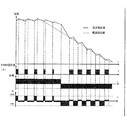
図2は、スイッチング関数Sc1(t)及びSc2(t)の決定要領を示している。このようにして、第1の曲線は、基準設定値電圧V*及び三角形キャリアVp(t)の時間の関数としての傾向を示す。これにより、第2の曲線は、時間の関数として、Sc1の傾向及び第3の曲線を示し、第2の曲線の補数を作成し、時間の関数として、Sc2を示すことにより推定される。第4の曲線は、+UDCから−UDCに変更し、一定間隔ごとに断続する周期fPWMの間の平均値V*を有する磁気回路10の端子における電圧Uactの傾向を示す。電圧Uactは、明確に異なる2つの値のみを取ることができるため、これは2値状態PWM方法と言われる。
FIG. 2 shows how to determine the switching functions Sc 1 (t) and Sc 2 (t). In this way, the first curve shows the trend as a function of the reference setpoint voltage V * and the triangular carrier V p (t). Thus, the second curve is estimated by showing the trend of Sc 1 and the third curve as a function of time, creating the complement of the second curve, and showing Sc 2 as a function of time. . The fourth curve shows the tendency of the voltage U act at the terminal of the
図3は、このタイプのPWM方法によって、負荷10の制御に対し、図1において示されているようなブリッジ1のトランジスタC2,C1,C4及びC3と、それぞれ同一である4つのスイッチAH,BH,AL及びBLを備えるフォー・クオドラントブリッジ11で誘導される切り替えについて説明している。
FIG. 3 shows four switches AH, BH respectively identical to the transistors C2, C1, C4 and C3 of the
ブリッジ11は、次の2つの可能な状態を有する。
− スイッチBH及びALが閉じており、スイッチAH及びBLが開いている磁化状態(アクチュエータに適用される電圧VL=+Udc)。
− スイッチBH及びALが開いており、スイッチAH及びBLが閉じている消磁状態(アクチュエータに適用される電圧VL=−Udc)。
The
A magnetized state in which the switches BH and AL are closed and the switches AH and BL are open (voltage V L = + U dc applied to the actuator).
A demagnetized state in which the switches BH and AL are open and the switches AH and BL are closed (voltage V L = −U dc applied to the actuator)
しかし、このようなPWM制御をフォー・クオドラントブリッジに対して実施すると、若干の問題が生じる。 However, when such PWM control is performed on the four quadrant bridge, there are some problems.
その第1の問題は、切り替え損失についてである。スイッチが切り替え状態を変更(開いた状態から閉じた状態への変更又は閉じた状態から開いた状態への変更)した際、それを流れる電流及び端子間の電圧が同時に存在するために損失を起こす。ついで消えるエネルギーは、DC電圧UDCの細断された電流lactの値、及び切り替えの速度の値(切り替え時間は、例えば、使用されるMOSFETトランジスタのゲート抵抗の値によって設定される)に依存する。このように、それぞれの一定間隔ごとに断続する周期に対して、各ブリッジレッグの2つのスイッチのうちの1つに流れる電流の方向に関わらず、2つの開放及び2つの閉鎖がある。それぞれの一定間隔ごとに断続する周期に対するこの2重の切り替えにより、明らかに、周波数が増加するのに従って、損失はより大きくなる。効率および帯域の幅を調整することが重要であることが分かる。PWM制御の場合、PWM周波数は、一般的に、数十又は数百キロヘルツである。これらの高周波数において、切り替え損失は、他の伝導損失に比して小である。磁化状態にから消磁状態へ変化する際に、それぞれの一定間隔ごとに断続する周期に対する4つの切り替え動作のうち、2つはハード切り替え動作であり、2つはソフト切り替え動作である。すなわち、第1の段階は、最初は閉じている2つのトランジスタを開くことであり(ハード切り替え)、それからデッドタイムの後、最初に開いている2つのトランジスタは閉じられる。全く同一のレッグを有する2つのスイッチを同時に閉じることは、このようにして回避される。デッドタイムの間(ソフト切り替えの前)、MOSFETスイッチに固有のダイオード(“フリーホイーリング”と呼ばれる)を処理し、ソフト切り替えの間、MOSFETの電位をゼロに近い状態で維持することを可能にする。 The first problem is about switching loss. When the switch changes its switching state (change from open to closed or change from closed to open), the current flowing through it and the voltage across the terminals are present, causing loss . The energy that then disappears depends on the value of the chopped current l act of the DC voltage U DC and the value of the switching speed (the switching time is set, for example, by the value of the gate resistance of the MOSFET transistor used) To do. Thus, there are two open and two close regardless of the direction of the current flowing through one of the two switches of each bridge leg for each periodic interval. Clearly, this double switching for intermittent periods at each regular interval will result in greater losses as the frequency increases. It can be seen that it is important to adjust the efficiency and bandwidth. In the case of PWM control, the PWM frequency is generally tens or hundreds of kilohertz. At these high frequencies, the switching loss is small compared to other conduction losses. When changing from the magnetized state to the demagnetized state, two of the four switching operations with respect to the intermittent cycle at each predetermined interval are the hard switching operation and the two are the soft switching operations. That is, the first stage is to open the two transistors that are initially closed (hard switching), and then after the dead time, the first two transistors that are open are closed. Closing two switches with exactly the same leg at the same time is thus avoided. During the dead time (before soft switching), it handles the diodes inherent to the MOSFET switch (called “freewheeling”), allowing the MOSFET potential to remain near zero during soft switching To do.
さらに、繰り返される切り替えにより、制御電子回路の効率に影響が及ぼされるだけではなく、駆動する電気機械の効率にも影響が及ぶ。電圧の一定間隔ごとの断続は、電気機械において損失を引き起こす高周波高調波を生成する。これらの電気機械は、一般的に、渦電流を生じる磁性材料(例えば、鉄−Si)から成っている。誘起電圧はプレート間において誘発される。プレートは、それらの固有抵抗のために、しばしば大きな渦電流を発生する。最後にプレートを切断し、別々に分離しても、そこで流れる電流は、ジュール効果により損失を生成する。上述のように、図2の第4の曲線は、電源9がUDCの値を有しているように、図1に示してあるように、負荷10の端子間において電圧UACTを示す。ブリッジの制御は、負荷サイクルαを伴うPWM型のものである。電圧UDCは、スイッチの電気抵抗による電圧効果を無視して負荷10に適用される。負荷サイクルが何であれ、後者が一定であれば、負荷10に適用される電圧の実効値(Ueddy)は、電圧UDC(ピーク電圧を示す電圧UACT)と等しく、UDC=Ueddyである。最終的に、一定間隔ごとに断続する周波数を超える周波数を有し、一定の負荷サイクルを考慮可能な渦電流によって生成される損失は、実質的に、ピーク電圧に比例しており、Peddy=k.Ueddy=k.UDCである。
Furthermore, repeated switching not only affects the efficiency of the control electronics, but also affects the efficiency of the driving electrical machine. Intermittent intervals of voltage generate high frequency harmonics that cause losses in the electrical machine. These electric machines are generally made of a magnetic material (eg, iron-Si) that produces eddy currents. An induced voltage is induced between the plates. Plates often generate large eddy currents due to their resistivity. Finally, even if the plate is cut and separated separately, the current flowing there generates losses due to the Joule effect. As described above, the fourth curve in FIG. 2 shows the voltage U ACT across the
さらに、電子機器の制御、特にそれらのスイッチは、一定間隔ごとの断続のために、高周波共通モード電流を生成する。負荷は、一般的に地面に対して静電結合を有する。例えば、コイルを巻きつけられた電気機械の場合、共通モード電圧がかけられたコイルと、接地したフレームとの間には大きな結合がある。共通モード電流は、このようにして生成され、それらは、電源によってループされる。これらの高周波電流ループは、現在のEMC(電磁両立性)規格に準拠する点で影響があるような電磁放射を引き起こす。 Furthermore, the control of the electronic equipment, particularly those switches, generate a high frequency common mode current for intermittent intervals. The load generally has an electrostatic coupling to the ground. For example, in the case of an electric machine wound with a coil, there is a large coupling between the coil applied with the common mode voltage and the grounded frame. Common mode currents are thus generated and they are looped by the power supply. These high frequency current loops cause electromagnetic radiation that has an impact on compliance with current EMC (electromagnetic compatibility) standards.
本発明は、電気制御部材における電流及び制御部材の端子間の電圧を制御し、電源スイッチの切り替え損失、及び磁気回路における渦電流と関連した損失を減らす経済的方法を提供し、上述したEMC問題を未然に防ぐ“フォー・クオドラント”ブリッジ回路を提供することを目的としている。 The present invention provides an economical way to control the current in the electrical control member and the voltage between the terminals of the control member to reduce the switching loss of the power switch and the loss associated with the eddy current in the magnetic circuit, and the EMC problem described above. The objective is to provide a “four quadrant” bridge circuit that prevents this.
この目的を達成するために、本発明は、電気制御部材における電流又は電気制御部材の端子間の電圧を制御する回路であって、
− 4つの端子と、4つの制御スイッチを備えるブリッジと、
− ブリッジのための電源と、
− パルス幅変調によって4つのスイッチのうち少なくとも2つを制御する手段
とを備え、
電源は、ブリッジの第1の端子及び第2の端子の間で接続され、
電気制御部材は、ブリッジの第3の端子及び第4の端子の間で接続され、
第1のスイッチは、ブリッジの第1の端子及び第3の端子の間で接続され、
第2のスイッチは、ブリッジの第1の端子及び第4の端子の間で接続され、
第3のスイッチは、ブリッジの第3の端子及び第2の端子の間で接続され、
第4のスイッチは、ブリッジの第4の端子及び第2の端子の間で接続されており、
制御回路は、
− 第1の状態は、第1及び第4のスイッチが閉じ、第2及び第3のスイッチが開いており、
− 第2の状態は、前記第2及び第3のスイッチが閉じ、前記第1及び第4のスイッチが開いており、
− 以下の2つの状態のうちの少なくとも1つであり、
○第3の状態は、第3及び第4のスイッチが閉じ、第1及び第2のスイッチが開いており、
○第4の状態は、第1及び第2のスイッチが閉じ、第3及び第4のスイッチが開いていることを特徴とし、
パルス幅変調制御手段は、
− 第1の状態から、第3又は第4の状態のうち少なくとも1つの状態への遷移、
− 第2の状態から、第3又は第4の状態のうち少なくとも1つの状態への遷移、
− 第3又は第4の状態のうち少なくとも1つの状態から、第1の状態への遷移、
− 第3又は第4の状態のうち少なくとも1つの状態から、第2の状態への遷移
を許すことを特徴とする回路を提供するものである。
In order to achieve this object, the present invention provides a circuit for controlling a current in an electric control member or a voltage between terminals of the electric control member,
-A bridge with four terminals and four control switches;
-A power supply for the bridge;
-Means for controlling at least two of the four switches by pulse width modulation;
A power source is connected between the first terminal and the second terminal of the bridge;
The electrical control member is connected between the third terminal and the fourth terminal of the bridge,
The first switch is connected between the first terminal and the third terminal of the bridge;
The second switch is connected between the first terminal and the fourth terminal of the bridge;
The third switch is connected between the third terminal and the second terminal of the bridge,
The fourth switch is connected between the fourth terminal and the second terminal of the bridge,
The control circuit
The first state is that the first and fourth switches are closed and the second and third switches are open;
The second state is when the second and third switches are closed and the first and fourth switches are open;
-At least one of the following two states:
○ In the third state, the third and fourth switches are closed, the first and second switches are open,
The fourth state is characterized in that the first and second switches are closed and the third and fourth switches are open,
The pulse width modulation control means
A transition from the first state to at least one of the third or fourth states;
A transition from the second state to at least one of the third or fourth states;
A transition from at least one of the third or fourth states to the first state;
The circuit is characterized by allowing a transition from at least one of the third or fourth states to the second state;
本発明によると、制御回路を、PWM方法によって制御される“フォー・クオドラント”ブリッジ(すなわち、回路は、3つ又は4つの異なる状態へ切り替えることに使用可能である)の3つ又は4つの状態の管理に使用することが可能である。上記のPWM方法は、負荷(電気制御部材)の端子に適用された電圧VLは、3つの段階、すなわち、−UDC,0及びUDC(UDCは電源によって供給される電圧を表す)に基づいているため、3状態と言われる。第3の状態の導入は、1つのハード切り替え(及び1つのソフト切り替え)を軽減する。2つのハード切り替えを導く、“磁化”状態及び“消磁”状態間における直接の遷移を回避するために、本発明に係る回路は、“磁化”状態から、いわゆる“フリーホイーリング”状態(第3又は第4の状態のに対応する)への遷移、及び“消磁”状態から、“フリーホイーリング”状態への遷移を可能とする。従って、切り替えの数は、2つの要因によって減らすことが可能である。このような現象は、パワーエレクトロニクスの設計に重大な影響を及ぼし、次のことを可能にする。
− 既存のパワーエレクトロニクスの信頼性における改善。
− 使用される構成部品の小型化。
− コストの削減。
According to the present invention, the control circuit is configured in three or four states of a “four quadrant” bridge (ie, the circuit can be used to switch to three or four different states) controlled by the PWM method. It can be used to manage In the above PWM method, the voltage VL applied to the terminal of the load (electrical control member) has three stages: -U DC , 0 and U DC (U DC represents the voltage supplied by the power supply). It is said to be in 3 states. The introduction of the third state alleviates one hard switch (and one soft switch). In order to avoid a direct transition between the “magnetized” state and the “demagnetized” state, which leads to the two hard switching, the circuit according to the present invention, from the “magnetized” state, the so-called “freewheeling” state (third Or corresponding to the fourth state) and transition from the “demagnetization” state to the “freewheeling” state. Therefore, the number of switching can be reduced by two factors. Such a phenomenon has a significant impact on the design of power electronics and enables:
− Improvements in the reliability of existing power electronics.
-Miniaturization of the components used;
-Cost reduction.
さらに、渦電流を通した損失について、実効値は、ブリッジを2つの状態に切り替えるフォー・クオドラントブリッジの従来の制御と、3つ又は4つの状態の間で、ブリッジを切り替える本発明によって提供される制御との間で、大いに異なっている。3つ又は4つの状態に制御することは、同じ電流を制御するのに、必要な電圧を減少させる。換言すると、すなわち、同じ平均電圧を供給することになる。 Furthermore, for losses through eddy currents, the rms value is provided by the conventional control of a four quadrant bridge that switches the bridge to two states and the present invention that switches the bridge between three or four states. There is a great difference between the controls. Controlling to three or four states reduces the voltage required to control the same current. In other words, the same average voltage is supplied.
さらに、上述したように、電気部材によって制御されるアクチュエータは、フレームに関して論理的に誤った電気容量を有している。電圧の断続は、制御電子回路において、地上を経て戻る高周波高調波を生成する。これは、共通モード外乱である。EMC規格は、この雑音レベルを制限している。本発明によれば、3状態制御によって生成される電圧は、2状態制御のものよりも、より少ない高調波を生成する。共通モード電流における6dBの低減は、このようにして達成される。 Furthermore, as described above, the actuator controlled by the electrical member has a logically wrong capacitance with respect to the frame. The intermittent voltage produces high frequency harmonics that return through the ground in the control electronics. This is a common mode disturbance. The EMC standard limits this noise level. According to the present invention, the voltage generated by the three state control generates fewer harmonics than that of the two state control. A 6 dB reduction in common mode current is thus achieved.
本発明に係るシステムも、個別又は技術的に可能な組み合わせの全てにおいて考えられる、次の特徴を備えている。 The system according to the invention also has the following features that can be considered individually or in all possible technical combinations.
パルス幅変調制御方法は、次のことを可能としていると有利である。
− 第1の、いわゆる、負の交番フェーズは、第1の状態から第3の状態への遷移、第3の状態から第1へ状態への遷移を許容し、第1及び第3の切り替えは第1のレッグ、いわゆる、振幅レッグを形成し、いわゆる、一定間隔ごとに断続する周波数で切り替わり、第2及び第4のトランジスタは、符号レッグと呼ばれる第2のレッグを形成し、それぞれのレッグは閉じており、開いている。
− 第2の、いわゆる、正の交番フェーズは、第2の状態から第4の状態への遷移、第4の状態から第1への遷移を許容し、第1及び第3のスイッチは、いわゆる、一定間隔ごとに断続する周波数で切り替わり、前記第2(BH)及び第4(BL)のスイッチも同様に切り替わり、符号レッグの第2及び第4のスイッチの切り替えは、一定間隔ごとに断続する周波数未満の周波数において、負及び正の交番間の遷移を確実にする。
The pulse width modulation control method advantageously allows the following:
The first so-called negative alternating phase allows a transition from the first state to the third state, a transition from the third state to the first state, the first and third switching being The first leg, the so-called amplitude leg, is switched at a so-called intermittent frequency, and the second and fourth transistors form a second leg, called the sign leg, each leg being Closed and open.
The second, so-called positive alternating phase allows a transition from the second state to the fourth state, a transition from the fourth state to the first, and the first and third switches are so-called The second (BH) and fourth (BL) switches are switched in the same manner, and the switching of the second and fourth switches of the code leg is intermittent at regular intervals. Ensure a transition between negative and positive alternating at frequencies below the frequency.
本発明に係る制御回路は、電気制御部材及び第4の端子の間で連続して接続される分流器を備えていると有利である。 The control circuit according to the invention advantageously comprises a shunt connected in series between the electrical control member and the fourth terminal.
この場合、制御回路は、必須のものとして、演算増幅器を備え、分流器の端子は、演算増幅器の反転及び非反転の入力を形成している。 In this case, the control circuit is essentially provided with an operational amplifier, and the terminals of the shunt form the inverting and non-inverting inputs of the operational amplifier.
本発明に係る制御回路は、次の要素を備えていると有利である。
− 充電された際に、第2のスイッチに対して制御電圧を供給するのに適するチャージポンプキャパシタ。
−第1の電源から供給される電圧よりも少ない電圧を供給する第2の電源であって、第4のスイッチが閉じている際、チャージポンプキャパシタを充電するのに適する第2の電源。
−チャージポンプキャパシタが第2の電源から再充電されるために制御回路が正の交番フェーズにあるとき、第4の状態から第3の状態への遷移を強いるための手段。
The control circuit according to the invention advantageously comprises the following elements:
A charge pump capacitor suitable for supplying a control voltage to the second switch when charged;
A second power supply for supplying a voltage less than that supplied by the first power supply, the second power supply being suitable for charging the charge pump capacitor when the fourth switch is closed;
Means for forcing a transition from the fourth state to the third state when the control circuit is in a positive alternating phase because the charge pump capacitor is recharged from the second power source;
本発明の第1の実施の形態によれば、制御手段は、次の要素を備えている。
− 負荷サイクルαを有するパルス幅変調信号を生成するための手段。
− 負荷サイクルαを有するパルス幅変調信号を第3のトランジスタに適用し、負荷サイクル1−αを有するパルス幅変調信号を第1のトランジスタに適用するための手段。
− 次のような状態を実現するために、正及び負の交番フェーズの間を通過するための手段であって、
○ブリッジが正の交番フェーズにあり、負荷サイクルαが取り消されるとき、装置は状態の変化を検出し、正の交番フェーズに変更し、
○ブリッジが負の交番フェーズにあり、負荷サイクルαが100%に等しいとき、装置は状態の変化を検出し、正の交番フェーズに変更するようになっているもの。
According to the first embodiment of the present invention, the control means includes the following elements.
Means for generating a pulse width modulated signal having a duty cycle α.
Means for applying a pulse width modulated signal having a duty cycle α to the third transistor and applying a pulse width modulated signal having the duty cycle 1-α to the first transistor;
-Means for passing between the positive and negative alternating phases to achieve the following conditions:
○ When the bridge is in the positive alternating phase and the duty cycle α is canceled, the device detects a change in state and changes to the positive alternating phase,
○ When the bridge is in the negative alternating phase and the duty cycle α is equal to 100%, the device detects a change in state and changes to the positive alternating phase.
電源は、DC電圧+UDCであって、制御回路は、次の要素を備えていると有利である。
− 正の交番フェーズの間、積α×UDCに等しい平均電圧を電気制御部材に適用するための手段。
− 負の交番フェーズの間、(α―1)×UDCと等しい平均電圧を電気制御部材に適用するための手段。
Advantageously, the power supply is DC voltage + U DC and the control circuit comprises the following elements:
- During the positive alternation phase, it means for applying an average voltage equal to the product alpha × U DC to the electrical control member.
- During the negative alternation phase, (α-1) × means for applying U DC equal average voltage to the electric control member.
第2の実施の形態によれば、制御手段は、次の諸要素を備えている。
− 負荷サイクルαを有するパルス幅変調信号を生成するための手段。
− 負荷サイクルαを有するパルス幅変調信号を、負荷サイクルα´=│2α―1│を有するパルス幅変調信号に変換するための手段。
− 負荷サイクルα´を有するパルス幅変調信号を第3のトランジスタ(AL)に適用し、正の交番フェーズの間、負荷サイクル1−α´を有するパルス幅変調信号を第1のトランジスタ(AH)に適用するための手段。
− 負荷サイクル1−α´を有するパルス幅変調信号を第3のトランジスタ(AL)に適用し、負の交番フェーズの間、負荷サイクルα´を有するパルス幅変調信号を第1のトランジスタ(AH)に適用するための手段。
− 次の状態の装置を実装する正及び負の交番フェーズの間を通過させるための手段であって、
○ブリッジが正の交番フェーズにあり、負荷サイクルαが正確に50%未満であるとき、装置は状態の変化を検出し、負の交番フェーズに変更し、
○ブリッジが負の交番フェーズにあり、負荷サイクルαが50%以上であるとき、装置は状態の変化を検出し、正の交番フェーズに変更するようになっているもの。
According to the second embodiment, the control means includes the following elements.
Means for generating a pulse width modulated signal having a duty cycle α.
Means for converting a pulse width modulated signal having a duty cycle α into a pulse width modulated signal having a duty cycle α ′ = | 2α−1 |
Applying a pulse width modulated signal having a duty cycle α ′ to the third transistor (AL) and applying a pulse width modulated signal having the duty cycle 1-α ′ to the first transistor (AH) during the positive alternating phase; Means to apply to.
Applying a pulse width modulated signal with duty cycle 1-α 'to the third transistor (AL) and applying a pulse width modulated signal with duty cycle α' to the first transistor (AH) during the negative alternating phase; Means to apply to.
Means for passing between the positive and negative alternating phases implementing the device in the next state, comprising:
○ When the bridge is in the positive alternating phase and the duty cycle α is exactly less than 50%, the device detects a change in state and changes to the negative alternating phase,
○ When the bridge is in the negative alternating phase and the duty cycle α is 50% or more, the device detects a change in state and changes to the positive alternating phase.
電源はDC電圧+UDCを供給し、制御回路は、積(2α―1)×UDCに等しい平均電圧を、正及び負の交番フェーズの間、電気制御部材に適用するための手段を備えていると有利である。 The power supply provides a DC voltage + U DC and the control circuit comprises means for applying an average voltage equal to the product (2α−1) × U DC to the electrical control member during the positive and negative alternating phases. It is advantageous to have.
負荷サイクルαを有するパルス幅変調信号を、負荷サイクルα´=│2α―1│を有するパルス幅変調信号に変換するための手段は、
− 負荷サイクルが50%に等しい信号及び負荷サイクルαの信号の間で減算を実行するための手段と、
− 減算によって得られる信号を倍増させるための手段とを備えていると有利である。
Means for converting a pulse width modulated signal having a duty cycle α into a pulse width modulated signal having a duty cycle α ′ = | 2α−1 |
-Means for performing a subtraction between a signal whose duty cycle is equal to 50% and a signal of duty cycle α;
It is advantageous to have means for doubling the signal obtained by subtraction.
負荷サイクルが50%に等しい信号、及び負荷サイクルαの信号の間で減算を実行するための手段は、それぞれ、負荷サイクル50%の信号、及び負荷サイクルαの信号である2つの入力を有する排他的論理和論理機能を実行する手段であるのが好ましい。 The means for performing a subtraction between a signal with a duty cycle equal to 50% and a signal with a duty cycle α is an exclusive having two inputs which are a signal with a duty cycle 50% and a signal with a duty cycle α, respectively. Preferably, it is a means for performing a logical OR function.
減算によって得られる信号を倍増させるための手段は、少なくとも1つのカウンタを備えていることが好ましい。 The means for doubling the signal obtained by subtraction preferably comprises at least one counter.
制御手段はプログラマブル論理回路に含まれていると有利である。 The control means is advantageously included in a programmable logic circuit.
スイッチはMOSFETトランジスタであると有利である。 The switch is advantageously a MOSFET transistor.
本発明の別の課題は、可変インダクタンスと共に誘導負荷によって形成される電気部材による制御回路の使用方法である。 Another subject of the present invention is a method of using a control circuit with an electrical member formed by an inductive load with a variable inductance.
電気部材は、動作部分を有するアクチュエータに含まれ、電気部材は、動作部分変位幅を制御するようになっていると有利である。 Advantageously, the electrical member is included in an actuator having an operating part, and the electrical member is adapted to control the operating part displacement width.
アクチュエータは、自動車用の電磁気バルブアクチュエータであるのが好ましい。 The actuator is preferably an electromagnetic valve actuator for an automobile.
本発明の上記以外の特徴及び効果は、添付図面を参照して以下に述べる本発明の非限定な例に関する説明により、明白になると思う。
すべての図において、共通の要素には、同じ符号を付してある。 In all the drawings, common elements are denoted by the same reference numerals.
図1〜図3については、従来技術の説明のために既に上述した。 1 to 3 have already been described above for the description of the prior art.
図4は、本発明に係る制御回路の3状態を示している。 FIG. 4 shows three states of the control circuit according to the present invention.
回路100は、
− 4つの端子105,106,107及び108と、
− 例えば、電池又はブリッジ1の第1の端子105及び第2の端子106間で接続されるDC−DC電力変換装置(又は、AC−DC電力変換装置)である、電圧+UDCを供給するDC電源109と、
− アクチュエータを制御するための誘導負荷のようであり、第3の端子107及び第4の端子108間で接続される電気制御部材110と、
− 第1の端子105及び第3の端子107の間で接続される第1のスイッチAHと、
− 第1の端子105及び第4の端子108の間で接続される第2のスイッチBHと、
− 第2の端子106及び第3の端子107の間で接続される第3のスイッチALと、
− 第2の端子106及び第4の端子108の間で接続される第4のスイッチBL
とを備えている。
The
-
- For example, supplies the 1 DC-DC power conversion device connected between
An
A first switch AH connected between the
A second switch BH connected between the
A third switch AL connected between the
A fourth switch BL connected between the
And.
電源スイッチAH、BH、AL及びBLは、例えば、MOSFETトランジスタである。各々のトランジスタは、逆並列取り付けダイオード(MOSFETトランジスタの場合における構造を有する)を備えている。 The power switches AH, BH, AL, and BL are, for example, MOSFET transistors. Each transistor comprises an antiparallel attached diode (having the structure in the case of a MOSFET transistor).
電気制御部材(以下、負荷とも呼ぶ)110は、この場合、電磁バルブのアクチュエータ(電磁石)を制御するのに使用される可変インダクタンスである。可変インダクタンスは明らかに完全ではなく、抵抗部分を含んでいる。電気制御部材110における電流は、例えば、バルブ(開閉それぞれの位置でバルブを維持するパドルを経由して)の開閉を制御するために使用される。バルブの位置は、設定値電流に対応する設定値によって決められる。
The electric control member (hereinafter also referred to as a load) 110 is a variable inductance used in this case to control the actuator (electromagnet) of the electromagnetic valve. The variable inductance is clearly not perfect and includes a resistive portion. The electric current in the
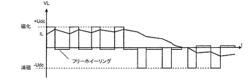
図4は、3状態(磁化、フリーホイーリング、消磁)を示している。
− 磁化状態は、トランジスタBH及びALが閉じており、トランジスタAH及びBLが開いている場合に相当する。この場合、負荷110の端子に適用される電圧VLは電圧+UDCである。
− フリーホイーリング状態は、トランジスタAL及びBLが閉じており、トランジスタAH及びBHが開いている状態に相当する。この状態は、下記で“低”フリーホイーリング状態と呼ばれる。これは、ここでは示されていない別のフリーホイーリング状態である“高”フリーホイーリング状態と呼ばれる状態と対比される。“高”フリーホイーリング状態は、トランジスタAH及びBHが閉じており、トランジスタAL及びBLが開いている状態である。高又は低フリーホイーリングの場合、負荷110の端子に適用される電圧VLは電圧0である。
− 消磁状態は、トランジスタAH及びBLが閉じており、トランジスタAL及びBHが開いている状態に相当する。この場合、負荷110の端子に適用される電圧VLは電圧−UDCである。
FIG. 4 shows three states (magnetization, freewheeling, demagnetization).
The magnetized state corresponds to the case where the transistors BH and AL are closed and the transistors AH and BL are open. In this case, the voltage V L applied to the terminals of the
The freewheeling state corresponds to the state in which the transistors AL and BL are closed and the transistors AH and BH are open. This state is referred to below as the “low” freewheeling state. This is in contrast to a state called the “high” freewheeling state, which is another freewheeling state not shown here. The “high” freewheeling state is a state in which transistors AH and BH are closed and transistors AL and BL are open. In the case of high or low freewheeling, the voltage V L applied to the terminal of the
The demagnetization state corresponds to the state in which the transistors AH and BL are closed and the transistors AL and BH are open. In this case, the voltage V L applied to the terminals of the
これら3つ(又は4つの)状態を導入する利点は、それぞれの周期において、切り替えの数を減らす方法を提供することである。磁化状態から消磁状態への変化は(逆の場合も同様に)、2回の切り替えを必要とする。その一方で、磁化状態又は消磁状態から(高又は低の)フリーホイーリング状態への変化には、1回の切り替えを必要とする。実際に、第1の場合において、2つのレッグは、同時にスイッチするが、他の場合には、1つだけのレッグがスイッチする。下記において、2つの低又は高フリーホイーリング状態を使用することが有利であることを示す。しかしながら、これら2つの状態(高又は低フリーホイーリング状態)は、同じ機能を実現し、2つのフリーホイーリング状態の内、1つの状態だけを使用することが可能でもある。低フリーホイーリング状態だけが使用されるため、この構成については図4に示してある。 The advantage of introducing these three (or four) states is to provide a way to reduce the number of switches in each cycle. A change from a magnetized state to a demagnetized state (and vice versa) requires two switches. On the other hand, a change from a magnetized state or a demagnetized state to a freewheeling state (high or low) requires one switching. In fact, in the first case, the two legs switch at the same time, while in other cases only one leg switches. In the following, it will be shown that it is advantageous to use two low or high freewheeling conditions. However, these two states (high or low freewheeling state) achieve the same function, and it is also possible to use only one of the two freewheeling states. Since only the low freewheeling state is used, this configuration is shown in FIG.
切り替えの数を軽減するため、磁化状態及び消磁状態の間に直接の状態変化はない。そのため、既定の切り替え回数の頻度に対して、切り替えの数を2回に減らすことが可能である。 To reduce the number of switches, there is no direct state change between the magnetized state and the demagnetized state. Therefore, the number of switching can be reduced to two with respect to the frequency of the predetermined number of switching.
図5及び図6は、図4に示す負荷110のような負荷の端子に適用される電圧VL、及びこの負荷における電流ILの傾きを、それぞれ、2状態を使用する技術の状態によるPWM制御の場合、及び3つの状態を使用する本発明に係る制御回路の場合をそれぞれ説明している。
FIGS. 5 and 6 show the voltage V L applied to the terminal of a load such as the
負荷における正又は負の電流ILを維持することは、2状態制御の場合、2つのクォードラント(磁化状態及び消磁状態にそれぞれ対応する正及び負の電圧交番+UDC及び−UDC)での動作を伴う。その結果、3状態を伴う電流の同じ制御は、ちょうど1つのクオドラント(正又は負の電圧交番であり、制御されている正又は負の電流に依存しているか否かに関わらず、フリーホイーリング状態に対応するほとんどゼロの電圧である)での本質的な稼働を可能にする。 Maintaining a positive or negative current I L at the load is in the case of two-state control with two quadrants (positive and negative voltage alternations + U DC and −U DC corresponding to the magnetized and demagnetized states, respectively). With movement. As a result, the same control of the current with the three states is exactly one quadrant (positive or negative voltage alternation, regardless of whether it depends on the positive or negative current being controlled. Allows for essential operation at almost zero voltage corresponding to the condition).
図4で示す様態では、低フリーホイーリング状態のみが使用され、2つのレッグA及びBは、PWM制御(通常数十又は数百kHz)の周波数で切り替わるようになっている。 In the mode shown in FIG. 4, only the low freewheeling state is used, and the two legs A and B are switched at a frequency of PWM control (usually tens or hundreds of kHz).
このような設定は、直接負荷電流測定において、いくつかの共通モード障害を引き起こす。まず図7を参照して、そのような測定を行うための回路200について簡単にに述べる。
Such a setting causes some common mode disturbances in direct load current measurements. First, a
回路200は、既に図4を参照して上述した構成要素に加えて、負荷110と直列に接続される分流器201を備えている。この分流器は、回路200の端子108及び演算増幅器202の非反転入力に連結される端子203、負荷110及び演算増幅器202の反転入力に連結される端子204を有する。
The
負荷における電流測定を直接行う利点は、平均電流制御を実装する際、平均電流のイメージを得るための電流を再構成する必要がないことである。また、分流器が安価な解決法であるため、高共通モード電圧を受ける演算増幅器の使用は重要である。このようにして、地面を基準とする測定方法が得られる。一方、位相は地面に対して強い電位変化を受ける。これは、高同相信号除去比(高CMRR)が、増幅器の出力で、ノイズの影響を受けない測定方法を有するために必要な理由である。測定方法のフィルタリングにより、共通モードノイズを減らすことができるが、帯域幅及び安定性について不利な状況にする。高帯域幅を有することが必要であり、かつ迅速な切り替えが必要な際には、特別の測定を行うことは困難である。 An advantage of performing current measurements directly at the load is that when implementing average current control, there is no need to reconstruct the current to obtain an image of the average current. Also, since shunts are an inexpensive solution, the use of operational amplifiers that receive high common mode voltages is important. In this way, a measurement method based on the ground is obtained. On the other hand, the phase undergoes a strong potential change with respect to the ground. This is the reason why a high common-mode rejection ratio (high CMRR) is necessary to have a measurement method that is insensitive to noise at the output of the amplifier. Common mode noise can be reduced by filtering the measurement method, but it is disadvantageous for bandwidth and stability. When it is necessary to have a high bandwidth and quick switching is required, it is difficult to make special measurements.
このようにして、2状態PWM制御を伴う回路200を使用することにより、電流の測定方法は、電流のレギュレーションを妨げる複数のスイッチそれぞれの切り替えにおいて、共通モードによるピークによってノイズの影響を受ける。
In this way, by using the
この問題を未然に防ぐための方法は、4つの可能な状態(磁化、消磁、高フリーホイーリング、低フリーホイーリング)の順序を定めすることにある。そのため、電流測定分流器201に連結されるレッグブリッジ(この場合レッグB)は、一定間隔ごとに断続する周波数において切り替わらない。
A way to prevent this problem is to determine the order of the four possible states (magnetization, demagnetization, high freewheeling, low freewheeling). Therefore, the leg bridge (in this case, leg B) connected to the
この方法については、図4で示す回路100におけるのと同一の構成要素によって形成されている制御回路300の4状態の順序を示す図8を参照して説明する。
This method will be described with reference to FIG. 8 which shows the sequence of the four states of the
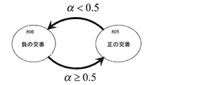
以後、フォー・クオドラント制御回路300の2つの巨視的な状態を区別する。
− “正の交番”という用語は、制御回路300が、スイッチAH,AL,BH及びBLを切り替える際、負荷110によって観察される平均電圧が正であるために、適用する。
− “負の交番”という用語は、制御回路がスイッチを切り替える際、負荷110によって観察される平均電圧が負であるために、適用する。正の平均電圧は、負荷において正の電流ILを導くこととなる。
Hereinafter, two macroscopic states of the four
The term “positive alternating” applies because the average voltage observed by the
-The term "negative alternation" applies because the average voltage observed by the
レッグAのみの切り替えによって得られる正の交番は、AH及びALをスイッチし、レッグBは、いつも同じ状態(BHは閉じており、BLは開いている)のまま切り替わる。すなわち、このようにして、磁化状態(AHは開いており、ALは閉じている)から高フリーホイーリング状態(AHは閉じており、ALは開いている)への正の交番の場合における変化があり、2つの状態間のその変化は、一定間隔ごとに断続する周波数(通常、数十あるいは数百kHz)で発生する。したがって、正の交番の間、レッグAのみが、高周波数(一定間隔ごとに断続する周波数)で切り替わり、レッグBは切り替わらない。 The positive alternation obtained by switching only leg A switches AH and AL, and leg B always switches in the same state (BH is closed and BL is open). That is, in this way, the change in the case of a positive alternation from the magnetized state (AH is open and AL is closed) to the high freewheeling state (AH is closed and AL is open). The change between the two states occurs at a frequency that is intermittent at regular intervals (usually tens or hundreds of kHz). Therefore, during the positive alternation, only leg A switches at a high frequency (frequency that is intermittent at regular intervals), and leg B does not switch.
正の交番から負の交番への変化は、レッグB(BHは開いており、BLは閉じている)を切り替えることによって得られる。 The change from a positive alternation to a negative alternation is obtained by switching leg B (BH is open and BL is closed).
負の交番は、スイッチAH及びALのみを切り替えることによって得られ、レッグBはいつも同じ状態(BHは開いており、BLは閉じている)のまま切り替わる。このようにして、磁化状態(AHは閉じており、ALは開いている)から、低フリーホイーリング状態(AHは開いており、ALは閉じている)への負の交番の場合における変化があり、2つの状態間のその変化は、一定間隔ごとに断続する周波数(通常、数十あるいは数百kHz)で発生する。負の交番の間では、正の交番の間のように、レッグAのみは、高周波数(一定間隔ごとに断続する周波数)に切り替わり、レッグBは切り替わらない。 A negative alternation is obtained by switching only switches AH and AL, and leg B always switches in the same state (BH is open and BL is closed). Thus, there is a change in the negative alternation from the magnetized state (AH closed and AL open) to the low freewheeling state (AH open and AL closed). Yes, the change between the two states occurs at frequencies that are intermittent at regular intervals (usually tens or hundreds of kHz). During the negative alternation, as in the positive alternation, only leg A is switched to a high frequency (frequency that is intermittent at regular intervals), and leg B is not switched.
磁化状態の継続時間、及び低フリーホイーリング状態の継続時間の間の比率がどうであれ、負荷110によって得られる平均電圧は正である。これは、“正の交番”という用語が、これら2つの状態間の切り替えを示すのに使用されるためである。
Whatever the ratio between the duration of the magnetized state and the duration of the low freewheeling state, the average voltage obtained by the
同様に、消磁状態の継続時間及びフリーホイーリング状態の継続時間の間の比率に関係なく、負荷110によって得られる平均電圧は負である。これは、“負の交番”という用語が、これら2つの状態間の切り替えを示すのに使用されるためである。
Similarly, regardless of the ratio between the duration of the degaussing state and the duration of the freewheeling state, the average voltage obtained by the
低フリーホイーリングと高フリーホイーリングとを区別することによって、同じ交番に対し、制御回路300の1つのレッグのみを切り替えることが可能である。
By distinguishing between low and high freewheeling, it is possible to switch only one leg of the
正の交番の間、レッグB(BHは閉じており、BLは開いている)は切り替わらず、それに対して、レッグAは、一定間隔ごとに断続する周波数で切り替わる。同様に、負の交番の間、レッグB(BHは開いており、BLは閉じている)は切り替わらず、それに対して、レッグAは、一定間隔ごとに断続する周波数で切り替わる。 During the positive alternation, leg B (BH is closed and BL is open) is not switched, while leg A is switched at an intermittent frequency at regular intervals. Similarly, during negative alternation, leg B (BH is open and BL is closed) is not switched, while leg A is switched at a frequency that is intermittent at regular intervals.
したがって、2つの交番の間、レッグBは切り替わらない。レッグBの切り替えは、負荷110に適用する平均電圧の符号が変化した際の交番の変更の場合にのみ発生する。2つの交番間における切り替わりは、一定間隔ごとに断続する周波数よりも十分下の周波数、及び電流レギュレーションの帯域幅よりも下の周波数で発生する。その周波数は、論理上は、一定間隔ごとに断続する周波数の2分の1未満であるが、一般的には一定間隔ごとに断続する周波数(通常、数kHz)の10分の1未満である。
Therefore, leg B does not switch between the two alternations. The switching of the leg B occurs only when the alternation is changed when the sign of the average voltage applied to the
そのため、電圧の振幅(絶対値)を調節するために切り替わる高周波へブリッジのレッグ(この場合はレッグA)が貢献することは可能であり、負荷に適用される電圧の極性に対して切り替わる低周波へ他のレッグ(この場合はレッグB)が貢献することは可能である Therefore, the bridge leg (in this case, leg A) can contribute to the high frequency that switches to adjust the amplitude (absolute value) of the voltage, and the low frequency that switches to the polarity of the voltage applied to the load. It is possible for another leg (in this case leg B) to contribute
以下において、振幅を調節するための振幅レッグ(レッグA)と、負荷に適用する電圧の極性に対する符号レッグ(レッグB)とを対比する。 In the following, the amplitude leg (Leg A) for adjusting the amplitude is compared with the sign leg (Leg B) for the polarity of the voltage applied to the load.
振幅レッグ及び符号レッグを使用することは、分流器を組み込んでいる制御回路の構成において、特に重要である。 The use of an amplitude leg and a sign leg is particularly important in the construction of control circuits incorporating shunts.
回路400のような正及び負の交番について、図9を参照して説明する。回路400は、図4を参照して既に述べた構成要素に加え、負荷110、回路200の端子108及び演算増幅器202の非反転入力に連結する端子203、及び負荷110及び演算増幅器202の反転入力に連結する端子204と直列に接続されている分流器201を備えている。スイッチAH及びALによって形成されるレッグAは、一定間隔ごとに断続する周波数でスイッチし、負荷110の電流の絶対値を設定するのに使用される振幅レッグである。スイッチBH及びBLによって形成されるレッグBは、符号レッグであり、正及び負の交番の間で変化を実行するのに使用される。
Positive and negative alternation as in
共通モード障害の発生は、先行技術における2段階構成のものよりも小さいため、この構成は特に重要である。障害は、符号交番の間でのみ発生する。物理的に、符号の変化は、電流の傾斜が実質的に反転した際に発生する。図10は、その動作を説明している。すなわち、付加の端子間にわたる電圧VL及び負荷(分流器201及び演算増幅器202を経由した)で測定される電流ILは、時間の関数として表わされる。正の交番AP(BLが処理する間、BLは閉じている)は、負の交番AN(BHが処理する間、BLは閉じている)によって、次のようになる。共通モード障害(ピーク電流が測定電流を阻害している)は、交番が変化するときにのみ発生する。上記で導かれるように、先行技術による2状態の構成と共に、それぞれの切り替えにおいて、ピークが観察される。
This configuration is particularly important because the occurrence of common mode failures is less than that of the two-stage configuration in the prior art. Failure occurs only between code alternations. Physically, the sign change occurs when the current slope is substantially reversed. FIG. 10 illustrates the operation. That is, the voltage V L across the additional terminals and the current I L measured at the load (via
図9及び図10に示す実施例は、交番の変化がない限り、符号レッグBの2つのトランジスタのうちの1つを常に閉じたままにすること意味している。したがって、符号レッグのトランジスタBHの閉鎖の制御は、正の定電流のレギュレーションの場合において、永続する可能性がある。MOSFET又は、IGBTトランジスタをこの閉鎖状態で維持するために、制御電圧は、そのゲートに適用されなければならない。トランジスタに制御電圧を適用する1つの解決方法は、いわゆるチャージポンプ技術を使用することにある。図11は、本発明に係る制御回路で使用され、トランジスタBH(レッグBのみ図11で示される)の制御電圧の維持を可能にするスイッチのチャージポンプ回路500を示している。回路500は、次の要素を備えている。すなわち、
− 主電源からの電圧UDCよりも低い電圧(通常、12〜15Vの順序によって、MOSFETトランジスタのゲートを制御するために使用される標準的な値に対応するこれらの電圧値)を供給する補助電源装置501。
− そのアノードが補助電源装置501に連結されているダイオード502。
− ダイオード502のカソードに連結される第1の端子、及びトランジスタBH、及びBLの共通端子に連結される第2の端子を有するキャパシタ503。
−ダイオード502のカソードに連結される第1の端子及びトランジスタBHのゲートに連結される第2の端子を有する第1のスイッチ504。
− 第1のスイッチ504の第2の端子に連結し、そのため、トランジスタBHのゲートに連結する第1の端子、及びトランジスタBH及びBLの共通端子に連結される第2の端子を有する第2のスイッチ505。
The embodiment shown in FIGS. 9 and 10 means that one of the two transistors of the sign leg B is always kept closed unless there is an alternating change. Thus, the control of the sign leg transistor BH closure may be permanent in the case of positive constant current regulation. In order to keep the MOSFET or IGBT transistor in this closed state, a control voltage must be applied to its gate. One solution for applying a control voltage to the transistor is to use so-called charge pump technology. FIG. 11 shows a
Auxiliary to supply voltages lower than the voltage U DC from the mains (usually those voltage values corresponding to the standard values used to control the gates of the MOSFET transistors, in the order of 12-15V).
A
A
A
A second terminal coupled to the second terminal of the
キャパシタ503は、補助電源501を経由してトランジスタBLを閉じることによってチャージされる。
The
チャージされたキャパシタ503は、スイッチ504が閉じている際、トランジスタBHのゲートを制御する電圧を供給する。
The charged
トランジスタBHを制御するためにチャージポンプ技術を使用すると、再充電することなく、ゲートでの電圧を恒久的に維持することができる。正の交番の継続時間が、一定の時間(正の電流を調整する際に可能な状態)を超える際には、符号レッグのトランジスタBHの閉鎖は、チャージポンプのキャパシタ503は徐々にトランジスタBHのゲートへ放電されるため、もはや保障されない。
Using charge pump technology to control transistor BH allows the voltage at the gate to be permanently maintained without recharging. When the duration of the positive alternation exceeds a certain time (a state that is possible when adjusting the positive current), the closing of the sign leg transistor BH causes the
このMOSFETの不要な開放を避けるための、1つの解決法として、符号レッグのトランジスタBLの閉鎖により、チャージドポンプのキャパシタ503の充電を保証する方法がある。
One solution for avoiding unnecessary opening of the MOSFET is to guarantee charging of the
負荷制御への阻害を避けるために、遷移は、高フリーホイーリング状態(ゼロ平均電圧が負荷によって観察される)の間で発生し、強制状態は、低フリーホイーリング状態(ゼロ平均電圧が負荷によって観察される)となる。負荷の制御は、高フリーホイーリング状態及び低フリーホイーリング状態が完全に負荷制御に関して等価であるため、そのような動作によっては阻害されない。このように、チャージポンプの再充電は、負荷(電気制御部材)に関して分かりやすい動作である。 To avoid hindrance to load control, transitions occur between high freewheeling states (zero average voltage is observed by the load), forced states are low freewheeling states (zero average voltage is loaded) Is observed). Load control is not hampered by such operation because the high freewheeling state and the low freewheeling state are completely equivalent with respect to load control. Thus, the recharging of the charge pump is an easy-to-understand operation regarding the load (electric control member).
チャージポンプのキャパシタ503は、このようにして、トランジスタBHで十分な制御電圧を維持するために再充電される。これに対して、符号レッグは、キャパシタ503がチャージポンプ回路500のダイオード502を通して、補助電源501により再充電されるのを可能にするトランジスタBLの制御に戻る。
The
次に、4状態(その2つである高フリーホイーリング、及び低フリーホイーリングは、負荷の観点から等価である)に伴う制御の2つの実施例について述べる。 Next, two embodiments of control with four states (two of which are high freewheeling and low freewheeling are equivalent from a load point of view) will be described.
その前に、フォー・クオドラントブリッジの2状態制御のレギュレーションループの動作について、簡単に再考しておく。ループ600は、図12に示されている。ループ600は、次の要素を備えている。
− 相殺器601。
− 増幅器602。
− 負荷サイクルαを有するPWM(パルス幅変調)信号の発生器603。
− 細断された電圧を負荷(通常、誘導負荷)605に供給するために、測定電流Imesは、ループ600によって閉ざされた電流を形成している、フォー・クオドラントブリッジ604。
Before that, let us briefly reconsider the operation of the two-state control regulation loop of the four quadrant bridge. The
-
An
A
A for
ブリッジ604の2状態制御のレギュレーションループ600は、次のように動作する。すなわち、電流設定値Irefを、閉ざされた電流Imesの測定値と比較する。相殺器601によって決定される電流設定値Irefと、閉ざされた電流Imesの測定値との差分Eは、増幅された差分Ea(増幅率Gは、比例ゲイン、積分ゲイン及び微分ゲインの組み合わせであり得る)を供給するための増幅率Gの増幅器602によって増幅する。増幅された誤差Eaは、キャリア、通常、振幅Aの三角形状又は鋸歯状の信号と比較する。それは、増幅された誤差によって変調されたパルス幅を伴うPWM信号を作り出すためである。フォー・クオドラントブリッジの切り替えは、このPWM信号(あるいは、PWM信号を補完する信号)によって、全く同一のレッグのスイッチの閉鎖及び開放の間のデッドタイムを監視することにより制御する。キャリア周波数で細断された電圧VLは、そのため、負荷605に適用される。負荷605に適用される平均電圧[数7]は、直接、負荷サイクルαに依存する。インダクタンスがL(線抵抗は無視される)である負荷605の電流ILは、この電圧を積分する。負荷における電流は、このようにして、増加させることができるが、あるいは電流の偏り、又は設定値の変化に対する逆の反応において減少させることができる。
The two-state
![]()
![]()
図13は、図12のレギュレーションループによって構成されている負荷サイクルαのPWM信号の構成を示す。PWM信号は、振幅A(この場合、鋸歯状の信号であるが、三角形状の信号でもよい)のキャリアと、増幅された誤差Eaによって示される有用な信号(変調装置)とを比較して構成される。キャリアは、一定間隔ごとに断続する周波数の設定に使用される。ブリッジ604に対する制御設定値を形成するPWM信号は、変調装置がキャリアよりも上、すなわちゼロよりも上にある限り、正のパルスを示す。PWM信号は、そのパルス長が誤差に依存する固定参照信号(キャリア信号)である。すなわち、負荷における電流を制御可能にするPWM信号の負荷サイクルである。この負荷サイクルは、[数8]の値(すなわち、負荷サイクルαを得るために、発生器603は増幅率1/Aを増幅された誤差Eaに適用する)を有する。
FIG. 13 shows the configuration of the PWM signal of the duty cycle α that is configured by the regulation loop of FIG. The PWM signal is configured by comparing a carrier having an amplitude A (in this case, a sawtooth signal, but may be a triangular signal) with a useful signal (modulation device) indicated by the amplified error Ea. Is done. The carrier is used for setting an intermittent frequency at regular intervals. The PWM signal that forms the control setpoint for
磁化状態及び消磁状態を説明する図3を参照すると、負荷サイクルαのPWM信号は、スイッチAL及びBHに適用され、PWM信号を補完する負荷サイクル1−αの信号は、スイッチAH及びBLに適用される。このようにして、磁化状態の間、DC電圧+Udcは継続時間αTの間、負荷に適用され、消磁状態の間、DC電圧−Udcは継続時間(1−α)Tの間、負荷に適用される。負荷10によって観察される平均電圧[数7]はそれ故、(2α―1)UDCとなる。図14は、図12に示されているような、2状態のレギュレーションループの場合における負荷サイクルαの関数として、負荷によって観察される平均電圧[数7]の線形の傾きを示している。
Referring to FIG. 3 for explaining the magnetized state and the demagnetized state, the PWM signal of the duty cycle α is applied to the switches AL and BH, and the signal of the duty cycle 1-α that complements the PWM signal is applied to the switches AH and BL. Is done. Thus, during the magnetized state, the DC voltage + U dc is applied to the load for a duration αT, and during the demagnetized state, the DC voltage −U dc is applied to the load for a duration (1−α) T. Applied. The average voltage [several 7] observed by the
2状態のレギュレーションループに関する先行技術について検討したので、次に、図15を参照して、本発明によって、4状態の制御回路を有効にするレギュレーションループ700の第1の実施例について述べる。
Having discussed the prior art regarding a two-state regulation loop, a first embodiment of a
レギュレーションループ700は、次の要素を備えている。
− 相殺器701。
− 増幅器702。
− 負荷サイクルαを有するPWM(パルス幅変調)信号の発生器703。
− 正の交番状態705又は負の交番状態706において、細断された電圧を負荷(通常、誘導負荷)707に供給し、その測定された電流Imesがループ700によって閉ざされた電流を形成するフォー・クオドラントブリッジ。
− 正の交番705及び負の交番706の間で変化させるための制御手段708。
The
-
An
A
-In positive alternating
A control means 708 for changing between a
レギュレーションループ700は、次のように動作する。すなわち、電流設定値lrefは、閉ざされた測定電流Imesと比較される。電流設定値Iref及び相殺器701によって決定される閉ざされた測定電流Imes間の差異Eは、増幅された差異Ea(増幅率Gは、比例ゲイン、積分ゲイン及び微分ゲインの組み合わせであり得る)を供給するための増幅率がGである増幅器702によって増幅される。増幅された誤差Eaは、発生器703によって増幅された誤差(αは、PWM信号の負荷サイクルを示す)によって変調されたパルス幅を伴うPWM信号を生成するために、振幅Aが通常、三角形状又は鋸歯状の信号であるキャリアと比較される。また、従来のPWM制御の場合のように、クオドラントブリッジの制御は、電流設定値及び電流測定値の間の誤差の関数であるとも言える。この差異はPWM関数内に存在し、ブリッジ状態は、PWM信号から決定されるサインに依存する。
The
正の交番705と負の交番706との間で変更するための制御手段708は、次の作用(図16で説明する)を実行する。
− ブリッジが正の交番705にあり、負荷サイクルが中止されたとき、機械は状態の変化を検出し、負の交番にスイッチする。すなわち、符号レッグは切り替わる。
− ブリッジが負の交番706にあり、負荷サイクルが1に等しいとき、機械は状態の変化を検出し、正の交番にスイッチする。すなわち、符号レッグは切り替わる。
The control means 708 for changing between the
-When the bridge is in the
-When the bridge is in a
図8に示すように、負荷サイクルαのPWM信号は、スイッチALに適用され、負荷サイクル(1−α)の補完PWM信号は、スイッチAHに正及び負の両方の交番の間において適用される。ブリッジが正の交番にあり、負荷サイクルが中止されたとき、手段708は、スイッチBHの開放及びスイッチBLの閉鎖を制御する。反対に、ブリッジが正の交番にあり、負荷サイクルが中止されたとき、手段708は、スイッチBLの開放及びスイッチBHの閉鎖を制御する。 As shown in FIG. 8, the duty cycle α PWM signal is applied to switch AL, and the duty cycle (1-α) complementary PWM signal is applied to switch AH during both positive and negative alternations. . When the bridge is in a positive alternation and the duty cycle is aborted, means 708 controls the opening of switch BH and the closing of switch BL. Conversely, when the bridge is in a positive alternation and the duty cycle is aborted, means 708 controls the opening of switch BL and the closing of switch BH.
手段708は符号レッグBを制御し、レッグが正の交番(正の符号信号)から負の交番(負の符号信号又はゼロ符号信号を選択することが可能)への切り替えを可能にする符号信号を使用すると有利である。
ブリッジの伝達機能は、正の交番にあるか、又は負の交番にあるかによって算出される。
− 正の交番
○磁化状態:電圧+Udcは、継続時間αT(TはPWM信号の周期を示す)の間で負荷に適用される。
○高フリーホイーリング状態:継続時間(1−α)Tの間で負荷に適用される負荷ゼロ電圧。
○その結果として、負荷によって観察される平均電圧は、正の交番の間では[数9]である。
The transfer function of the bridge is calculated depending on whether it is in a positive alternation or a negative alternation.
-Positive alternating ○ Magnetized state: The voltage + U dc is applied to the load during the duration αT (T indicates the period of the PWM signal).
O High freewheeling state: Zero load voltage applied to the load for a duration (1-α) T.
As a result, the average voltage observed by the load is [Equation 9] during positive alternation.
![]()
○消磁状態:電圧−Udcは継続時間(1−α)Tの間で負荷に適用される。
○低フリーホイーリング状態:継続時間αTの間で負荷に適用される負荷ゼロ電圧。
○その結果として、負荷によって観察される平均電圧は、負の交番の間では[数10]である。
![]()
O Low freewheeling state: Zero load voltage applied to the load for a duration αT.
As a result, the average voltage observed by the load is [Equation 10] during the negative alternation.
![]()
![]()
すなわち、本発明のこの実施の形態に係る制御回路は、次の手段を備えている。
− 正の交番705の間、平均電圧を積α×UDCに等しい負荷に適用する手段。
− 負の交番706の間、平均電圧を積(α−1)×UDCに等しい負荷に適用する手段。
That is, the control circuit according to this embodiment of the present invention includes the following means.
- During the
- During the
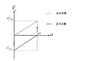
図17は、フォー・クオドラントブリッジの伝達機能を示している。すなわち、平均電圧[数7]は、図15で示すような2状態のレギュレーションループの場合、負荷サイクルαに従って、負荷により観察される。平均電圧の線形の挙動は、交番のそれぞれにおいて、一方の交番から、他方の交番(負荷サイクルが中止され制御回路が正の交番にあるとき、又は負荷サイクルが1に等しく制御回路が負の交番にあるときのいずれか)への切り替えが可能になることが明確に観察される。 FIG. 17 shows the transmission function of the four quadrant bridge. That is, the average voltage [Equation 7] is observed by the load according to the duty cycle α in the case of a two-state regulation loop as shown in FIG. The linear behavior of the average voltage is as follows: for each alternation, from one alternation to the other (when the duty cycle is stopped and the control circuit is in the positive alternation, or when the duty cycle is equal to 1 and the control circuit is negative It is clearly observed that it is possible to switch to
図18〜図21は、測定電流Imes、電流設定値Iref、負荷サイクルαのPWM信号、符号レッグBが正の交番(正の符号信号)から、負の交番(負の符号信号)に切り替えることを可能にする符号信号、異なる設定において、時間の関数として負荷の端子における電圧VLを示し得る。 18 to 21 show that the measured current I mes , the current set value I ref , the PWM signal of the duty cycle α, and the sign leg B change from a positive alternating signal (positive sign signal) to a negative alternating signal (negative sign signal). The sign signal that allows switching, in different settings, may indicate the voltage V L at the terminal of the load as a function of time.
図18は、電流設定値が突然降下する際、設定値と測定値との差が増加することを示している。この差は負である。誤差は増幅される。PWM信号の負荷サイクルは、その最小値(0%)まで誤差に応じて減少する。符号信号は、最初は正(正の交番)であり、負荷サイクルはゼロであるため、状態機械は状態の変化を検出する。符号信号は切り替わって、負になる。図17の伝達関数は、ゼロの負荷サイクル及び負の交番に対して、誘導負荷に適用された平均電圧が負であり、その振幅は最大であることを示している。測定電流は、設定値に向かって収束するために、急激に減少する。測定電流が設定値に近づくにつれて、誤差は減少し、負荷サイクルは増加する。そのため、電圧の振幅の減少を引き起こす。 FIG. 18 shows that the difference between the set value and the measured value increases when the current set value suddenly drops. This difference is negative. The error is amplified. The duty cycle of the PWM signal decreases according to the error to its minimum value (0%). Since the sign signal is initially positive (positive alternating) and the duty cycle is zero, the state machine detects a change in state. The sign signal switches and becomes negative. The transfer function of FIG. 17 shows that for zero duty cycle and negative alternation, the average voltage applied to the inductive load is negative and its amplitude is maximum. The measurement current decreases rapidly to converge toward the set value. As the measured current approaches the set point, the error decreases and the duty cycle increases. This causes a decrease in voltage amplitude.
図19に示すように、電流設定値が突然上昇する際、設定値と測定値との差は増加している。この差は正である。誤差は増幅される。負荷サイクルは、増幅された誤差に応じて増加し、その最大値に到達する。符号信号は、最初は正(正の交番)であり、負荷サイクルは最大であるため、機械は、いかなる状態の変化も検出しない。負荷に適用された電圧は、このようにして、電流が設定値に向かって収束可能なその最大値に到達する。増幅された誤差は、測定電流が設定値に近づくにつれて減少する。 As shown in FIG. 19, when the current set value suddenly increases, the difference between the set value and the measured value increases. This difference is positive. The error is amplified. The duty cycle increases with the amplified error and reaches its maximum value. Since the sign signal is initially positive (positive alternating) and the duty cycle is maximum, the machine does not detect any change in state. The voltage applied to the load thus reaches its maximum value at which the current can converge toward the set value. The amplified error decreases as the measured current approaches the set value.
図20に示すように、設定値が突然上昇する際、設定値と測定値との差は増加している。この差は正である。誤差は増幅される。負荷サイクルは誤差に応じて増加し、最大値に到達する。状態機械は、符号信号が最初は負であったことに対し、負荷サイクルが最大値(100%)であることを検出する。符号信号は切り替わり、正になる。図17のフォー・クオドラントブリッジの伝達関数は、最大振幅が正の電圧を表している。この電圧は、測定電流が増加して、設定値に追いつくことを可能にする。電流が設定値に近づくにつれて、誤差は減少し、そのため負荷サイクルは減少する。 As shown in FIG. 20, when the set value suddenly increases, the difference between the set value and the measured value increases. This difference is positive. The error is amplified. The duty cycle increases with error and reaches a maximum value. The state machine detects that the duty cycle is maximum (100%), whereas the sign signal was initially negative. The sign signal switches and becomes positive. The transfer function of the four quadrant bridge in FIG. 17 represents a voltage having a positive maximum amplitude. This voltage allows the measured current to increase and catch up with the set point. As the current approaches the set point, the error decreases and so the duty cycle decreases.
図21に示すように、設定値が突然減少する際、設定値と測定値との差は増加している。この差は負である。誤差は増幅される。負荷サイクルは、増幅された誤差に応じて減少し、最小値に到達する。符号信号は最初は負であるため、状態機械はいかなる変化も検出しない。フォー・クオドラントブリッジの伝達関数は、適用された平均電圧が負であることを表している。誘導負荷の端子間における負の電圧の振幅は、電流を急激に減少させる最大値となる。測定電流が設定値に近づくにつれ、誤差は減少し、負荷サイクルは再度増加する。負荷に適用された電流もまた、電流が設定値に向かって収束可能なその最大値に到達する。増幅された誤差は、測定電流が設定値に近づくにつれて減少する。この例では、符号の変化はない。 As shown in FIG. 21, when the set value suddenly decreases, the difference between the set value and the measured value increases. This difference is negative. The error is amplified. The duty cycle decreases with the amplified error and reaches a minimum value. Since the sign signal is initially negative, the state machine does not detect any change. The transfer function of the four quadrant bridge shows that the applied average voltage is negative. The amplitude of the negative voltage between the terminals of the inductive load is the maximum value that causes the current to decrease rapidly. As the measured current approaches the set point, the error decreases and the duty cycle increases again. The current applied to the load also reaches its maximum value at which the current can converge toward the set value. The amplified error decreases as the measured current approaches the set value. In this example, there is no sign change.
図15〜図21に関する解の場合、静誤差は、正の交番と負の交番との間で異なる。このようにして、負荷の端子間において全く同一の平均電圧[数7]を生成するために、誤差は2つの交番の場合において異なる。
正の交番の場合においては、[数11]である。
For the solutions with respect to FIGS. 15-21, the static error differs between positive and negative alternations. In this way, the error is different in the case of two alternations in order to produce the exact same average voltage [Equation 7] between the terminals of the load.
In the case of a positive alternation, [Equation 11].
![]()
![]()
![]()
![]()
負の静誤差は、正の静誤差よりも大きく、例えば、もし電源電圧が49Vであり、1Vが負荷の端子間で設定された場合、比率は50である。これは、電圧変動範囲において不連続であることを示している。それ以後、交番間の変化の間での電流の脱同期化が発生するおそれがある。この主要な静誤差は、しかしながら、静的増幅率における増加によって相殺される。 The negative static error is larger than the positive static error. For example, if the power supply voltage is 49V and 1V is set between the terminals of the load, the ratio is 50. This indicates that the voltage variation range is discontinuous. Thereafter, current de-synchronization may occur between changes between alternations. This major static error, however, is offset by an increase in static gain.
図22は、本発明に係る4状態制御回路を実装するため、及びこの静誤差問題を未然に防ぐためのレギュレーションループ800の第2の実施の形態を示す。 FIG. 22 shows a second embodiment of a regulation loop 800 for implementing the four-state control circuit according to the present invention and for preventing this static error problem.
レギュレーションループ800は、次の要素を備えている。
− 相殺器801。
− 増幅器802。
− 負荷サイクルαを有するPWM(パルス幅変調)信号の発生器803。
− 負荷サイクルαのPWM信号を負荷サイクルα’に変換するため(及び負荷サイクルα’のPWM信号を補完する負荷サイクル[数16]のPWM信号を供給するため)の変換器809。
The regulation loop 800 includes the following elements.
-
An
A
A
![]()
− 正の交番805及び負の交番806の間で切り替えるための制御手段808。
![]()
A control means 808 for switching between a
レギュレーションループ800は、次のように動作する。すなわち、電流設定値Irefを、閉じられた電流Imesの測定値と比較する。相殺器801によって決定される電流設定値Irefと、閉じられた電流の測定値Imesとの間における差異Eを、増幅された差異Ea(増幅率Gは、比例ゲイン、積分ゲイン及び微分ゲインの組み合わせであり得る)を供給するための増幅率がGである増幅器802によって増幅する。増幅された誤差Eaを、キャリア、通常、三角形状又は鋸歯状の信号と比較する。それにより、発生器803を経由して、パルス幅が増幅された誤差(αはPWM信号の負荷サイクルを示す)によって変調されたPWM信号が作り出される。
The regulation loop 800 operates as follows. That is, the current set value I ref is compared with the measured value of the closed current I mes . The difference Ea between the current set value I ref determined by the
負荷サイクルαのPWM信号は、[数17]と等しい負荷サイクルα’と同じ周波数の別のPWM信号を得るために、変換器809によって変換される。
The PWM signal of duty cycle α is converted by
![]()
![]()
変換器809は、例えば、50%の負荷サイクルのPWM信号と、負荷サイクルαのPWM信号との間で減算を実行するための手段を備えている。得られたPWM信号は、負荷サイクル[数18]を有する。
The
この減算は、図23で示すように、排他的論理和論理機能によって得ることができる。排他的論理和機能の入力は、50%の負荷サイクル、及び負荷サイクルαのPWM信号を有する同期化PWM信号であり、負荷サイクル[数18]のPWM信号は、出力において直接得られる。 This subtraction can be obtained by an exclusive OR function as shown in FIG. The input of the exclusive OR function is a synchronized PWM signal having a 50% duty cycle and a duty cycle α PWM signal, and the duty cycle [Equation 18] PWM signal is obtained directly at the output.
変換器809もまた、負荷サイクル[数18]のPWM信号を倍増する手段を有する。すなわち、得られた信号は、パルス幅が2倍に増えたPWM信号である。従って、負荷サイクルは、[数17]である。最終的に変換器809は、負荷サイクルαのPWM信号を、負荷サイクル[数19]と同じ周波数のPWM信号に変換する。
The
![]()
![]()
PWM信号を倍増させるのに使用されるこれらの手段は、2つのカウンタを使用して形成することができる。これらのカウンタの使用は、図24で説明される。 These means used to double the PWM signal can be formed using two counters. The use of these counters is illustrated in FIG.
負荷サイクル(α―1/2)の処理可能な信号から始まり、処理可能な信号の上昇端で得られた信号(倍増された信号)は、高い状態に変化し、第1のカウンタは、クロックにより調整されて、パルス幅の継続時間中増加し、それから停止する。落下端では、第2のカウンタが増加する(第1のカウンタと同じクロックにより調整されて)。この第2のカウンタの値が、第1のカウンタの値と等しくなったとき、得られた信号は取り消される。得られた信号は、処理可能な信号のパルス幅の2倍のパルス幅を有する。 Starting from the processable signal of the duty cycle (α-1 / 2), the signal obtained at the rising edge of the processable signal (doubled signal) changes to a high state and the first counter is clocked , And increases for the duration of the pulse width, then stops. At the falling edge, the second counter increments (adjusted by the same clock as the first counter). When the value of the second counter becomes equal to the value of the first counter, the obtained signal is canceled. The resulting signal has a pulse width twice that of the processable signal.
正の交番805と負の交番806とを切り替えるための制御手段808は、次の状態(図25で説明した)を取る。
− ブリッジが正の交番805にあり、負荷サイクルαが正確に50%未満であるとき、状態の変化を検出し、負の交番に切り替える。すなわち、符号レッグは切り替わる。
− ブリッジが負の交番806にあり、負荷サイクルαが50%以上のとき、状態の変化を検出し、正の交番に切り替える。すなわち、符号レッグは切り替わる。
The control means 808 for switching between the
When the bridge is in the
-When the bridge is in the
図8に示すように、正の交番(αは50%以上)の間、負荷サイクルα’のPWM信号は、スイッチALに送られ、負荷サイクル(1−α’)の補完的なPWM信号は、スイッチAHに送られる。 As shown in FIG. 8, during the positive alternation (α is 50% or more), the PWM signal of the duty cycle α ′ is sent to the switch AL, and the complementary PWM signal of the duty cycle (1−α ′) is , Sent to the switch AH.
負の交番(αは正確に50%未満である)の間、負荷サイクル1−α’のPWM信号は、スイッチALに送られ、負荷サイクルα’の補完的なPWM信号は、スイッチAHに送られる。 During the negative alternation (α is exactly less than 50%), the PWM signal of duty cycle 1-α ′ is sent to switch AL and the complementary PWM signal of duty cycle α ′ is sent to switch AH. It is done.
ブリッジが正の交番にあり、負荷サイクルαが正確に50%未満のとき、手段808は、スイッチBHの開放及びスイッチBLの閉鎖を制御する。反対に、ブリッジが正の交番にあり、負荷サイクルαが50%以上のとき、手段808は、スイッチBLの開放及びスイッチBHの閉鎖を制御する。 When the bridge is in a positive alternation and the duty cycle α is exactly less than 50%, the means 808 controls the opening of the switch BH and the closing of the switch BL. Conversely, when the bridge is in a positive alternation and the duty cycle α is greater than 50%, the means 808 controls the opening of the switch BL and the closing of the switch BH.
手段808は、レッグを正の交番(正の符号信号)から、負の交番(負の符号信号、又はゼロの符号信号が選択可能)に切り替え可能にすることによって、符号レッグBを制御するための符号信号を使用すると有利である。 Means 808 controls sign leg B by allowing the leg to switch from a positive alternation (a positive sign signal) to a negative alternation (a negative sign signal or a zero sign signal can be selected). It is advantageous to use the following code signal.
ブリッジの伝達関数は、正の交番にあるか、又は負の交番にあるかによって算出される。
− 正の交番:
・磁化状態:バス電圧+Udcは、継続時間[数20]の間、負荷に供給される。
The transfer function of the bridge is calculated depending on whether it is in a positive alternation or a negative alternation.
-Positive police box:
Magnetized state: The bus voltage + U dc is supplied to the load for the duration [Equation 20].
![]()
![]()
![]()
![]()
![]()
・磁化状態:バス電圧−Udcは、継続時間[数23]の間、負荷に供給される。
![]()
Magnetized state: The bus voltage -U dc is supplied to the load for the duration [Equation 23].
![]()
![]()
![]()
![]()
![]()
![]()
すなわち、本発明のこの実施の形態に係る制御回路は、積(2α―1)×UDCと等しい平均電圧を正の交番805、及び負の交番806の間、負荷に適用する手段を備えている。
That is, the control circuit according to this embodiment of the present invention, the product (2α-1) × U DC equal average voltage during the
図26は、フォー・クオドラントブリッジの伝達関数、すなわち、図22において示されるような4状態のレギュレーションループの場合における負荷サイクルαに従う負荷によって観察される平均電圧[数7]を示す。平均電圧の線形の挙動を、明確に観察することができる。すなわち、この伝達関数は、負荷サイクルの変換がなされているという事実を除いて、既知の2状態フォー・クオドラントブリッジのための制御のものと同一である。この伝達関数によって静誤差問題は解決可能であることが、その対称性によって、容易に理解し得ると思う。 FIG. 26 shows the four quadrant bridge transfer function, ie, the average voltage [Equation 7] observed by the load following the duty cycle α in the case of a four-state regulation loop as shown in FIG. The linear behavior of the average voltage can be clearly observed. That is, this transfer function is identical to that of the control for the known two-state for quadrant bridge, except for the fact that duty cycle conversion has been made. It can be easily understood that the static error problem can be solved by this transfer function due to its symmetry.
制御戦略(図15によるレギュレーションループを使用する制御回路の場合及び図22によるレギュレーションループを使用する制御回路の場合の両方)を可能にする多様な制御手段は、例えば、FGPA(field programmable gate array)に組み込まれた論理手段である。 Various control means enabling a control strategy (both in the case of a control circuit using the regulation loop according to FIG. 15 and in the case of a control circuit using the regulation loop according to FIG. 22) are, for example, field programmable gate arrays (FGPA) It is a logical means built in.
本発明は、上に記載した実施の形態だけに限定されるものではないことは言うまでもない。 It goes without saying that the present invention is not limited to the embodiments described above.
以上、本発明を、電磁気バルブアクチュエータへ適用した場合について説明したが、本発明は、例えば、電気モータのような誘導負荷によって制御されるいかなる種類の電気機械にも適用し得るものである。 As described above, the case where the present invention is applied to an electromagnetic valve actuator has been described. However, the present invention can be applied to any kind of electric machine controlled by an inductive load such as an electric motor.
電気機械へ適用した場合、その機械は、単相でも三相でもよい。 When applied to an electrical machine, the machine may be single phase or three phase.
さらに、本発明の実施の形態として、誘導負荷における電流の制御に関して説明してきたが、本発明は、この同じ負荷の端子間における電圧の制御にも適用し得ることは明らかである。 Furthermore, although the control of the current in the inductive load has been described as the embodiment of the present invention, it is obvious that the present invention can be applied to the control of the voltage between the terminals of the same load.
さらに、FPGAが、状態機械を実装するためにプログラムされている適用例について述べたが、この状態機械を、結線論理を使用することにより実装することも可能である。 Furthermore, although an application has been described in which an FPGA is programmed to implement a state machine, it is also possible to implement this state machine by using connection logic.
以上本発明を、MOSFETトランジスタを使用している場合について詳しく述べた。しかし、他のタイプのトランジスタ(たとえば、IGBT)もまた、本発明の技術思想から逸脱することなく適用し得ることは言うまでもない。 The present invention has been described in detail for the case where MOSFET transistors are used. However, it will be appreciated that other types of transistors (eg, IGBTs) can also be applied without departing from the inventive concept of the present invention.
最後に、前記したいかなる構成要素も、等価の要素と、置換えできることは言うまでもない。 Finally, it goes without saying that any component described above can be replaced by an equivalent element.
10…磁気回路(負荷)
100…制御回路
109…DC電源
110…電気制御部材
201…電流測定分流器
202…演算増幅器、
5,6,7,8,105,106,107,108,203,204…端子、
300…フォー・クオドラント制御回路、
400…回路、
500…チャージポンプ回路、
501…補助電源装置、
502…ダイオード、
503…キャパシタ、
504,505…スイッチ、
600,700,800…レギュレーションループ、
601,701,801…相殺器、
602,702,802…増幅器、
603,703,803…発生器、
604…フォー・クオドラントブリッジ、
605…負荷、
708,808…制御手段、
809…変換器、
9…電源
AH…第1のスイッチ
BH…第2のスイッチ
AL…第3のスイッチ
BL…第4のスイッチ
10 ... Magnetic circuit (load)
DESCRIPTION OF
5, 6, 7, 8, 105, 106, 107, 108, 203, 204 ... terminals,
300 ... Four quadrant control circuit,
400 ... circuit,
500 ... Charge pump circuit,
501 ... Auxiliary power supply,
502 ... a diode,
503: Capacitor,
504, 505 ... switch,
600, 700, 800 ... regulation loop,
601, 701, 801...
602, 702, 802 ... amplifiers,
603, 703, 803 ... generators,
604 ... Four Quadrant Bridge,
605 ... Load,
708, 808 ... control means,
809 ... Converter,
9 ... Power source AH ... First switch BH ... Second switch AL ... Third switch BL ... Fourth switch
Claims (17)
− 4つの端子(105,106,107,108)と、4つの制御スイッチ(AH,AL,BH,BL)を備えるブリッジと、
− 前記ブリッジのための電源(109)と、
− パルス幅変調によって、前記4つのスイッチの中の少なくとも2つを制御する手段とを備え、
前記電源(109)は、前記ブリッジの第1の端子(105)及び第2の端子(106)の間で接続され、
前記電気制御部材(110)は、前記ブリッジの第3の端子(107)及び第4の端子(108)の間で接続され、
前記第1のスイッチ(AH)は、前記ブリッジの前記第1の端子(105)及び前記第3の端子(107)の間で接続され、
前記第2のスイッチ(BH)は、前記ブリッジの前記第1の端子(105)及び前記第4の端子(108)の間で接続され、
前記第3のスイッチ(AL)は、前記ブリッジの前記第3の端子(107)及び前記第2の端子(106)の間で接続され、
前記第4のスイッチ(BL)は、前記ブリッジの前記第4の端子(108)及び前記第2の端子(106)の間で接続されている前記回路において、
この回路は、
− 前記第1(AH)及び第4(BL)のスイッチが閉じ、前記第2(BH)及び第3(AL)のスイッチが開いている第1の状態、
− 前記第2(BH)及び第3(AL)のスイッチが閉じ、前記第1(AH)及び第4(BL)のスイッチが開いている第2の状態、
− 以下の2つの状態のうちの少なくとも1つの状態、
○ 前記第3(AL)及び第4(BL)のスイッチは閉じ、前記第1(AH)及び第2(BH)のスイッチは開いている第3の状態、
○ 前記第1(AH)及び第2(BH)のスイッチは閉じ、前記第3(AL)及び第4(BL)のスイッチは開いている第4の状態を取り、
前記パルス幅変調制御手段は、
− 前記第1の状態から、前記第3又は第4の状態のうち少なくとも1つの状態への遷移、
− 前記第2の状態から、前記第3又は第4の状態のうち少なくとも1つの状態への遷移、
− 前記第3又は第4の状態のうち少なくとも1つの状態から、前記第1の状態への遷移、
− 前記第3又は第4の状態のうち少なくとも1つの状態から、前記第2の状態への遷移を許容するようになっていることを特徴とする回路(100,200,30,400,600,700)。 A circuit (100, 200, 300, 400, 600, 700) for controlling a current in the electric control member (110) or a voltage between terminals of the electric control member,
-A bridge with four terminals (105, 106, 107, 108) and four control switches (AH, AL, BH, BL);
-A power supply (109) for said bridge;
-Means for controlling at least two of the four switches by pulse width modulation;
The power source (109) is connected between the first terminal (105) and the second terminal (106) of the bridge,
The electrical control member (110) is connected between a third terminal (107) and a fourth terminal (108) of the bridge;
The first switch (AH) is connected between the first terminal (105) and the third terminal (107) of the bridge,
The second switch (BH) is connected between the first terminal (105) and the fourth terminal (108) of the bridge,
The third switch (AL) is connected between the third terminal (107) and the second terminal (106) of the bridge,
In the circuit, the fourth switch (BL) is connected between the fourth terminal (108) and the second terminal (106) of the bridge.
This circuit is
A first state in which the first (AH) and fourth (BL) switches are closed and the second (BH) and third (AL) switches are open;
A second state in which the second (BH) and third (AL) switches are closed and the first (AH) and fourth (BL) switches are open;
-At least one of the following two states:
A third state in which the third (AL) and fourth (BL) switches are closed and the first (AH) and second (BH) switches are open;
O The first (AH) and second (BH) switches are closed, the third (AL) and fourth (BL) switches are in the open fourth state,
The pulse width modulation control means includes
A transition from the first state to at least one of the third or fourth states;
A transition from the second state to at least one of the third or fourth states;
A transition from at least one of the third or fourth states to the first state;
A circuit (100, 200, 30, 400, 600, characterized by allowing a transition from at least one of the third or fourth states to the second state) 700).
− 第1の、いわゆる負の交番フェーズは、前記第1の状態から前記第3の状態への遷移及び前記第3の状態から前記第1の状態への遷移を許容し、前記第1(AH)及び第3(AL)のスイッチは、振幅レッグ(A)と呼ばれる第1のレッグを形成し、いわゆるチョッピング周波数で切り替わり、前記第2(BH)及び第4(BL)のトランジスタは、符合レッグ(B)と呼ばれる第2のレッグを形成し、それぞれ閉じておりかつ開いており、
− 第2の、いわゆる正の交番フェーズは、前記第2の状態から前記第4の状態への遷移及び前記第4の状態から前記第1の状態への遷移を許容し、前記第1(AH)及び第3(AL)のスイッチは、前記いわゆるチョッピング周波数で切り替わり、前記第2(BH)及び第4(BL)のスイッチは前記符号レッグ(B)の前記第2(BH)及び第4(BL)スイッチを切り替え、これにより、前記チョッピング周波数未満の周波数で前記負及び正の交番間の遷移を確実にするようになっていることを特徴とする、請求項1に記載の制御回路(300,400,600,700)。 The pulse width modulation control means is a control circuit having characteristics that allow the following:
The first so-called negative alternating phase allows a transition from the first state to the third state and a transition from the third state to the first state, the first (AH ) And the third (AL) switch form a first leg called an amplitude leg (A), which switches at a so-called chopping frequency, and the second (BH) and fourth (BL) transistors are matched leg Forming a second leg called (B), each closed and open;
The second, so-called positive alternating phase, allows a transition from the second state to the fourth state and a transition from the fourth state to the first state, and the first (AH ) And third (AL) switches at the so-called chopping frequency, and the second (BH) and fourth (BL) switches are the second (BH) and fourth (B) of the code leg (B). The control circuit (300) according to claim 1, characterized in that the BL) switch is switched to thereby ensure a transition between the negative and positive alternating at a frequency below the chopping frequency. , 400, 600, 700).
前記演算増幅器の反転入力、及び非反転入力を形成する前記分流レジスタ(201)の端子とを備えることを特徴とする請求項3に記載の制御回路(400)。 An operational amplifier (202);
4. The control circuit (400) of claim 3, comprising a terminal of the shunt register (201) forming an inverting input and a non-inverting input of the operational amplifier.
− 前記第4のスイッチ(BL)が閉じた際に前記チャージポンプキャパシタを充電するのに適し、前記第1の電源によって供給される電圧よりも低い電圧を供給する第2の電源(501)と、
− 前記チャージポンプキャパシタが前記第2の電源から再充電されるために前記制御回路が正の交番フェーズにあるとき、前記第4の状態から前記第3の状態への遷移を強いる手段とを備えることを特徴とする請求項2〜4のいずれか1項に記載の制御回路(400)。 A charge pump capacitor (503) suitable for supplying a control voltage to the second switch (BH) when charged;
A second power supply (501) suitable for charging the charge pump capacitor when the fourth switch (BL) is closed and supplying a voltage lower than that supplied by the first power supply; ,
Means for forcing a transition from the fourth state to the third state when the control circuit is in a positive alternating phase because the charge pump capacitor is recharged from the second power source. Control circuit (400) according to any one of claims 2 to 4, characterized in that.
− 負荷サイクルαを有するパルス幅変調信号を生成するための手段(701,702,703)と、
− 前記負荷サイクルαを有する前記パルス幅変調信号を前記第3のトランジスタ(AL)に適用し、負荷サイクル1−αを有するパルス幅変調信号を前記第1のトランジスタ(AH)に適用するための手段(705,706)と、
− 次の状態装置を実装し、前記正及び負の交番フェーズの間を通過するための手段(708)とを備え、
前記状態装置は、
○ 前記ブリッジが正の交番フェーズにあり、負荷サイクルαが取り消されるとき、前記装置は状態の変化を検出し、負の交番フェーズに変更し、
○ 前記ブリッジが負の交番フェーズにあり、負荷サイクルαが100%に等しいとき、前記装置は状態の変化を検出し、正の交番フェーズに変更するようになっていることを特徴とする、請求項2〜5のいずれか1項に記載の制御回路(700)。 The control means includes
-Means (701, 702, 703) for generating a pulse width modulated signal having a duty cycle α;
Applying the pulse width modulation signal having the duty cycle α to the third transistor (AL) and applying the pulse width modulation signal having the duty cycle 1-α to the first transistor (AH). Means (705, 706);
Means for implementing (708) the next state machine and passing between said positive and negative alternating phases;
The state machine is
O When the bridge is in the positive alternating phase and the duty cycle α is canceled, the device detects a change in state and changes to the negative alternating phase;
O When the bridge is in a negative alternating phase and the duty cycle α is equal to 100%, the device detects a change in state and changes to a positive alternating phase, Item 6. The control circuit (700) according to any one of Items 2 to 5.
− 前記正の交番フェーズの間、積α×UDCと等しい平均電圧を、前記電気制御部材に適用するための手段(705)と、
− 前記負の交番フェーズの間、(α―1)×UDCと等しい平均電圧を、前記電気制御部材に適用するための手段(706)とを備えることを特徴とする、請求項6に記載の制御回路(700)。 Wherein the power source supplies a DC voltage + U DC,
- during the positive alternation phase, the average voltage equal to the product alpha × U DC, means for applying said electrical control member and (705),
-Means (706) for applying an average voltage equal to (α-1) x U DC during the negative alternating phase to the electrical control member. Control circuit (700).
− 負荷サイクルαを有する前記パルス幅変調信号を生成する手段(801,802,803)と、
− 負荷サイクルαを有する前記パルス幅変調信号を、負荷サイクルα´=│2α―1│を有するパルス幅変調信号に変換するための手段(809)と、
− 負荷サイクルα´を有する前記パルス幅変調信号を、前記第3のトランジスタ(AL)に適用し、前記正の交番フェーズの間、負荷サイクル1−α´を有するパルス幅変調信号を、前記第1のトランジスタ(AH)に適用するための手段(805)と、
− 負荷サイクル1−α´を有する前記パルス幅変調信号を、前記第3のトランジスタ(AL)に適用し、前記負の交番フェーズの間、前記負荷サイクルα´を有する前記パルス幅変調信号を、前記第1のトランジスタ(AH)に適用するための手段(806)と、
− 次の状態装置を実装し、前記正及び負の交番フェーズの間を通過するための手段(808)とを備え、
前記状態装置は、
○ 前記ブリッジが前記正の交番フェーズにあり、前記負荷サイクルαが正確に50%未満であるとき、前記装置は状態の変化を検出し、前記負の交番フェーズに変更し、
○ 前記ブリッジが前記負の交番フェーズにあり、前記負荷サイクルαが50%以上であるとき、前記装置は状態の変化を検出し、前記正の交番フェーズに変更するようになっていることを特徴とする、請求項2〜5のいずれか1項に記載の制御回路(800)。 The control means includes
-Means (801, 802, 803) for generating said pulse width modulated signal having a duty cycle α;
Means (809) for converting said pulse width modulated signal having duty cycle α into a pulse width modulated signal having duty cycle α ′ = | 2α−1 |
Applying the pulse width modulation signal having a duty cycle α ′ to the third transistor (AL), the pulse width modulation signal having a duty cycle 1-α ′ during the positive alternating phase, Means (805) for applying to one transistor (AH);
Applying the pulse width modulation signal having a duty cycle 1-α ′ to the third transistor (AL), and during the negative alternating phase, the pulse width modulation signal having the duty cycle α ′, Means (806) for applying to the first transistor (AH);
A means (808) for implementing the next state machine and passing between said positive and negative alternating phases;
The state machine is
O When the bridge is in the positive alternating phase and the duty cycle α is exactly less than 50%, the device detects a change in state and changes to the negative alternating phase;
○ When the bridge is in the negative alternating phase and the duty cycle α is 50% or more, the device detects a change in state and changes to the positive alternating phase. A control circuit (800) according to any one of claims 2 to 5.
積(2α―1)×UDCに等しい平均電圧を、前記正及び負の交番フェーズの間、前記電気制御部材に適用するための手段を備えていることを特徴とする、請求項8に記載の制御回路(800)。 Wherein the power source supplies a DC voltage + U DC,
The product (2α-1) equals the average voltage × U DC, between said positive and negative alternation phase, characterized in that it comprises means for applying said electrical control member, according to claim 8 Control circuit (800).
− 負荷サイクルが50%に等しい信号と前記負荷サイクルαの信号との間で減算を実行するための手段と、
− 前記減算によって得られる信号を倍増させるための手段
とを備えることを特徴とする、請求項7又は8に記載の制御回路。 The means for converting the pulse width modulated signal having a duty cycle α to the pulse width modulated signal having a duty cycle α ′ = | 2α−1 |
Means for performing a subtraction between a signal with a duty cycle equal to 50% and a signal of said duty cycle α;
9. Control circuit according to claim 7 or 8, characterized in that it comprises means for doubling the signal obtained by the subtraction.
Applications Claiming Priority (2)
| Application Number | Priority Date | Filing Date | Title |
|---|---|---|---|
| FR0708562A FR2924873B1 (en) | 2007-12-07 | 2007-12-07 | CIRCUIT FOR MONITORING THE CURRENT IN AN ELECTRICAL CONTROL OR TERMINAL VOLTAGE OF THE CONTROL ELECTRICAL DEVICE |
| PCT/FR2008/001695 WO2009101292A1 (en) | 2007-12-07 | 2008-12-04 | Circuit for controlling the current in an electrical control member or the voltage across the terminals of the said electrical control member |
Publications (2)
| Publication Number | Publication Date |
|---|---|
| JP2011507463A true JP2011507463A (en) | 2011-03-03 |
| JP2011507463A5 JP2011507463A5 (en) | 2013-03-07 |
Family
ID=39731783
Family Applications (1)
| Application Number | Title | Priority Date | Filing Date |
|---|---|---|---|
| JP2010536504A Pending JP2011507463A (en) | 2007-12-07 | 2008-12-04 | Circuit for controlling the current flowing through the electric control member or the voltage between the terminals of the electric control member |
Country Status (7)
| Country | Link |
|---|---|
| US (1) | US8576581B2 (en) |
| EP (1) | EP2227855A1 (en) |
| JP (1) | JP2011507463A (en) |
| KR (1) | KR20100089872A (en) |
| CN (1) | CN101889387B (en) |
| FR (1) | FR2924873B1 (en) |
| WO (1) | WO2009101292A1 (en) |
Families Citing this family (12)
| Publication number | Priority date | Publication date | Assignee | Title |
|---|---|---|---|---|
| FR2961964B1 (en) * | 2010-06-25 | 2012-07-13 | Valeo Sys Controle Moteur Sas | METHOD FOR CHARGING ACCUMULATION MEANS AND CORRESPONDING CHARGE DEVICE |
| CN102005908B (en) * | 2010-11-22 | 2015-10-07 | 中国石油大学(北京) | Pulse switch control device and control method |
| FR2970108B1 (en) * | 2010-12-30 | 2013-01-11 | Valeo Sys Controle Moteur Sas | ELECTROMAGNETIC DEVICE AND CORRESPONDING ELECTROMAGNETIC ACTUATOR. |
| US8782624B2 (en) * | 2011-12-15 | 2014-07-15 | Micron Technology, Inc. | Methods and systems for detection in a state machine |
| FR2986341B1 (en) * | 2012-01-31 | 2014-03-14 | Continental Automotive France | CONTROL OF AN INDUCTIVE LOAD BY MODULATION OF PULSE WIDTH |
| JP6260587B2 (en) * | 2015-06-29 | 2018-01-17 | トヨタ自動車株式会社 | Power supply |
| US9780675B2 (en) * | 2015-12-11 | 2017-10-03 | General Electric Company | System and method for controlling current in a power converter |
| WO2018182432A1 (en) * | 2017-03-28 | 2018-10-04 | Auckland Uniservices Limited | Ac-ac converter |
| CA3096554A1 (en) * | 2018-04-23 | 2019-10-31 | Assa Abloy Entrance Systems Ab | Drive arrangement for door operator |
| DE102020203318A1 (en) * | 2020-03-16 | 2021-09-16 | Siemens Mobility GmbH | Vehicle, in particular rail vehicle |
| KR102506089B1 (en) * | 2020-12-10 | 2023-03-03 | 현대오토에버 주식회사 | Motor control apparatus for alternating freewheeling and control method of alternating freewheeling for motor |
| CN115833579B (en) * | 2023-02-09 | 2023-05-02 | 中国人民解放军国防科技大学 | Chopper and maglev train |
Citations (8)
| Publication number | Priority date | Publication date | Assignee | Title |
|---|---|---|---|---|
| JPS59179489U (en) * | 1983-05-13 | 1984-11-30 | 三洋電機株式会社 | Pulse width modulation inverter |
| US6119046A (en) * | 1997-02-04 | 2000-09-12 | Deutsches Zentrum Fur Luft-Und Raumfahrt E.V. | Method of controlling a chopper driver and a circuit arrangement for executing the method |
| JP2003047284A (en) * | 2001-07-30 | 2003-02-14 | Nikon Corp | Switching element abnormality detector, pwm amplifier, motor driver, stage apparatus, exposure system, device manufactured by this exposure system, and method of manufacturing device |
| JP2004201453A (en) * | 2002-12-20 | 2004-07-15 | Nissan Motor Co Ltd | Drive unit of direct-current, three-phase brushless motor |
| DE10328623A1 (en) * | 2003-06-25 | 2005-01-27 | Siemens Ag | Converter circuit for (dis)charge of capacitive and/or piezoelectric adjuster for motor vehicle IC engine fuel injection system, comprises bridge circuit coupled to small buffer capacitor, larger storage capacitor and transformer |
| JP2005354873A (en) * | 2004-06-14 | 2005-12-22 | Alps Electric Co Ltd | Motor drive controller |
| US20060221648A1 (en) * | 2005-03-31 | 2006-10-05 | Chang Gung University | Modified high-efficiency phase shift modulation method |
| JP2007529190A (en) * | 2004-03-12 | 2007-10-18 | エムケイエス インストゥルメンツ, インコーポレイテッド | Control circuit for switching power supply |
Family Cites Families (8)
| Publication number | Priority date | Publication date | Assignee | Title |
|---|---|---|---|---|
| US7616046B2 (en) * | 2002-01-30 | 2009-11-10 | Koninklijke Philips Electronics N.V. | System comprising an electrical bridge for generating an electrical signal for a load and a control unit for such a system |
| JP4156324B2 (en) * | 2002-09-30 | 2008-09-24 | ローム株式会社 | DC-AC converter and AC power supply method |
| JP2004201485A (en) * | 2002-11-29 | 2004-07-15 | Sony Corp | Motor and controller of actuator |
| US20040239401A1 (en) * | 2003-05-27 | 2004-12-02 | Chi-Shun Liao | Zero-voltage-switching full-bridge converter |
| US7272020B2 (en) * | 2004-02-20 | 2007-09-18 | Northeastern University | Isolated, current-fed, pulse width modulation, DC-DC converter |
| US7283379B2 (en) * | 2005-01-07 | 2007-10-16 | Harman International Industries, Incorporated | Current controlled switch mode power supply |
| DE102005036769A1 (en) * | 2005-08-04 | 2007-02-08 | Siemens Ag | Method for checking an inductive load |
| US7529109B2 (en) * | 2006-06-23 | 2009-05-05 | Anpec Electronics Corporation | Driving circuit for switching DC power |
-
2007
- 2007-12-07 FR FR0708562A patent/FR2924873B1/en not_active Expired - Fee Related
-
2008
- 2008-12-04 KR KR1020107012616A patent/KR20100089872A/en not_active Application Discontinuation
- 2008-12-04 EP EP08872282A patent/EP2227855A1/en not_active Withdrawn
- 2008-12-04 CN CN200880119482.5A patent/CN101889387B/en not_active Expired - Fee Related
- 2008-12-04 WO PCT/FR2008/001695 patent/WO2009101292A1/en active Application Filing
- 2008-12-04 JP JP2010536504A patent/JP2011507463A/en active Pending
- 2008-12-04 US US12/745,845 patent/US8576581B2/en not_active Expired - Fee Related
Patent Citations (8)
| Publication number | Priority date | Publication date | Assignee | Title |
|---|---|---|---|---|
| JPS59179489U (en) * | 1983-05-13 | 1984-11-30 | 三洋電機株式会社 | Pulse width modulation inverter |
| US6119046A (en) * | 1997-02-04 | 2000-09-12 | Deutsches Zentrum Fur Luft-Und Raumfahrt E.V. | Method of controlling a chopper driver and a circuit arrangement for executing the method |
| JP2003047284A (en) * | 2001-07-30 | 2003-02-14 | Nikon Corp | Switching element abnormality detector, pwm amplifier, motor driver, stage apparatus, exposure system, device manufactured by this exposure system, and method of manufacturing device |
| JP2004201453A (en) * | 2002-12-20 | 2004-07-15 | Nissan Motor Co Ltd | Drive unit of direct-current, three-phase brushless motor |
| DE10328623A1 (en) * | 2003-06-25 | 2005-01-27 | Siemens Ag | Converter circuit for (dis)charge of capacitive and/or piezoelectric adjuster for motor vehicle IC engine fuel injection system, comprises bridge circuit coupled to small buffer capacitor, larger storage capacitor and transformer |
| JP2007529190A (en) * | 2004-03-12 | 2007-10-18 | エムケイエス インストゥルメンツ, インコーポレイテッド | Control circuit for switching power supply |
| JP2005354873A (en) * | 2004-06-14 | 2005-12-22 | Alps Electric Co Ltd | Motor drive controller |
| US20060221648A1 (en) * | 2005-03-31 | 2006-10-05 | Chang Gung University | Modified high-efficiency phase shift modulation method |
Also Published As
| Publication number | Publication date |
|---|---|
| FR2924873B1 (en) | 2011-11-25 |
| US8576581B2 (en) | 2013-11-05 |
| US20100270998A1 (en) | 2010-10-28 |
| KR20100089872A (en) | 2010-08-12 |
| CN101889387A (en) | 2010-11-17 |
| FR2924873A1 (en) | 2009-06-12 |
| CN101889387B (en) | 2014-04-23 |
| EP2227855A1 (en) | 2010-09-15 |
| WO2009101292A1 (en) | 2009-08-20 |
Similar Documents
| Publication | Publication Date | Title |
|---|---|---|
| JP2011507463A (en) | Circuit for controlling the current flowing through the electric control member or the voltage between the terminals of the electric control member | |
| CN102655372B (en) | Variable input voltage pfc circuit, system and there is the power supply of phase shift power rail | |
| US5428522A (en) | Four quadrant unipolar pulse width modulated inverter | |
| CN210093111U (en) | Switched mode power supply | |
| US5111378A (en) | DC chopper converter | |
| US8378633B2 (en) | MultiChannel DC controller operating independently of output power in critical conduction mode | |
| CN103916013B (en) | DC-DC Converter and operation method thereof | |
| US6160388A (en) | Sensing of current in a synchronous-buck power stage | |
| Schellekens et al. | Dead-time compensation for PWM amplifiers using simple feed-forward techniques | |
| CN104852559A (en) | Phase fault detection in switching power converters | |
| TWI542131B (en) | Switchable buck converter with?zero voltage switching capability operating with a stabilized switching frequency | |
| US20150097544A1 (en) | System and Method for Controlling a Power Supply | |
| JP2003511005A (en) | Pulse width modulated bridge circuit in a second bridge circuit | |
| CN114301268A (en) | Dynamic biasing techniques for current sensing based on enhanced MOSFET on-resistance | |
| JP2011507463A5 (en) | ||
| CN104426451A (en) | Driving circuit for an electric motor | |
| Achary et al. | A simple voltage modulator scheme for torque ripple minimization in a permanent magnet brushless DC motor | |
| CN105765855A (en) | Regulation of electrical generator output | |
| Liske et al. | Analysis and modeling of the Quasi-Z-Source-Inverter | |
| US7161819B2 (en) | Zero-crossing correction in sinusoidally commutated motors | |
| US8207695B2 (en) | Control circuit of a full-bridge stage | |
| Himmelstoss et al. | A simple two-quadrant DC motor controller | |
| CN112271976A (en) | Motor current control method based on bridge circuit | |
| US10587192B2 (en) | DC-DC voltage reducing converter with a test mode operation | |
| US11713134B2 (en) | Power supply for aircraft systems |
Legal Events
| Date | Code | Title | Description |
|---|---|---|---|
| A621 | Written request for application examination |
Free format text: JAPANESE INTERMEDIATE CODE: A621 Effective date: 20111115 |
|
| A521 | Written amendment |
Free format text: JAPANESE INTERMEDIATE CODE: A523 Effective date: 20130116 |
|
| A977 | Report on retrieval |
Free format text: JAPANESE INTERMEDIATE CODE: A971007 Effective date: 20130724 |
|
| A131 | Notification of reasons for refusal |
Free format text: JAPANESE INTERMEDIATE CODE: A131 Effective date: 20130730 |
|
| A601 | Written request for extension of time |
Free format text: JAPANESE INTERMEDIATE CODE: A601 Effective date: 20131029 |
|
| A602 | Written permission of extension of time |
Free format text: JAPANESE INTERMEDIATE CODE: A602 Effective date: 20131106 |
|
| A521 | Written amendment |
Free format text: JAPANESE INTERMEDIATE CODE: A523 Effective date: 20131202 |
|
| A02 | Decision of refusal |
Free format text: JAPANESE INTERMEDIATE CODE: A02 Effective date: 20140513 |