JP2011198822A - Cooling device for heating element - Google Patents

Cooling device for heating element Download PDF

Info

Publication number
JP2011198822A
JP2011198822A JP2010061159A JP2010061159A JP2011198822A JP 2011198822 A JP2011198822 A JP 2011198822A JP 2010061159 A JP2010061159 A JP 2010061159A JP 2010061159 A JP2010061159 A JP 2010061159A JP 2011198822 A JP2011198822 A JP 2011198822A
Authority
JP
Japan
Prior art keywords
fitting portion
seal member
cooling device
fitting
flow path
Prior art date
Legal status (The legal status is an assumption and is not a legal conclusion. Google has not performed a legal analysis and makes no representation as to the accuracy of the status listed.)
Granted
Application number
JP2010061159A
Other languages
Japanese (ja)
Other versions
JP5589468B2 (en
Inventor
Takashi Hirota
崇 広田
Akihiro Shibuya
彰弘 渋谷
Current Assignee (The listed assignees may be inaccurate. Google has not performed a legal analysis and makes no representation or warranty as to the accuracy of the list.)
Nissan Motor Co Ltd
Original Assignee
Nissan Motor Co Ltd
Priority date (The priority date is an assumption and is not a legal conclusion. Google has not performed a legal analysis and makes no representation as to the accuracy of the date listed.)
Filing date
Publication date
Application filed by Nissan Motor Co Ltd filed Critical Nissan Motor Co Ltd
Priority to JP2010061159A priority Critical patent/JP5589468B2/en
Publication of JP2011198822A publication Critical patent/JP2011198822A/en
Application granted granted Critical
Publication of JP5589468B2 publication Critical patent/JP5589468B2/en
Expired - Fee Related legal-status Critical Current
Anticipated expiration legal-status Critical

Links

Images

Classifications

    • HELECTRICITY
    • H01ELECTRIC ELEMENTS
    • H01LSEMICONDUCTOR DEVICES NOT COVERED BY CLASS H10
    • H01L24/00Arrangements for connecting or disconnecting semiconductor or solid-state bodies; Methods or apparatus related thereto
    • H01L24/01Means for bonding being attached to, or being formed on, the surface to be connected, e.g. chip-to-package, die-attach, "first-level" interconnects; Manufacturing methods related thereto
    • H01L24/26Layer connectors, e.g. plate connectors, solder or adhesive layers; Manufacturing methods related thereto
    • H01L24/31Structure, shape, material or disposition of the layer connectors after the connecting process
    • H01L24/33Structure, shape, material or disposition of the layer connectors after the connecting process of a plurality of layer connectors
    • HELECTRICITY
    • H01ELECTRIC ELEMENTS
    • H01LSEMICONDUCTOR DEVICES NOT COVERED BY CLASS H10
    • H01L2924/00Indexing scheme for arrangements or methods for connecting or disconnecting semiconductor or solid-state bodies as covered by H01L24/00
    • H01L2924/10Details of semiconductor or other solid state devices to be connected
    • H01L2924/11Device type
    • H01L2924/13Discrete devices, e.g. 3 terminal devices
    • H01L2924/1304Transistor
    • H01L2924/1305Bipolar Junction Transistor [BJT]
    • H01L2924/13055Insulated gate bipolar transistor [IGBT]

Landscapes

  • Engineering & Computer Science (AREA)
  • Computer Hardware Design (AREA)
  • Microelectronics & Electronic Packaging (AREA)
  • Power Engineering (AREA)
  • Cooling Or The Like Of Semiconductors Or Solid State Devices (AREA)
  • Cooling Or The Like Of Electrical Apparatus (AREA)

Abstract

【課題】冷媒の漏出を有効に防止できる発熱素子の冷却装置を提供する。
【解決手段】発熱素子2が配置される主面と、放熱部41および該放熱部を周囲する第1嵌合部43が形成された他の主面とを有する第1放熱体4と、第1放熱体と組み合わせることで、放熱部41を受容して冷媒流路を形成する受容部51と、受容部を周囲する第2嵌合部53とを有する第2放熱体5と、第1嵌合部43と第2嵌合部53との間に介装され、冷媒流路をシールするシール部材6と、を備える発熱素子の冷却装置であって、第1嵌合部43と第2嵌合部53との間には、冷媒流路と異なる側に、シール部材6により、冷媒流路から隔てられた間隙100が形成されており、間隙100には、少なくとも一部に、シール部材6の配置位置における第1嵌合部43と第2嵌合部53との間の幅よりも、幅の狭い部分である幅狭部が形成されていることを特徴とする発熱素子の冷却装置。
【選択図】 図6
A cooling device for a heating element capable of effectively preventing refrigerant leakage is provided.
A first radiator 4 having a main surface on which a heat generating element 2 is disposed, and another main surface on which a heat radiating portion 41 and a first fitting portion 43 surrounding the heat radiating portion are formed; In combination with the first radiator, the second radiator 5 having the receiving portion 51 that receives the heat radiating portion 41 to form the refrigerant flow path, and the second fitting portion 53 surrounding the receiving portion, and the first fitting A cooling device for a heating element, comprising a sealing member 6 interposed between the joint portion 43 and the second fitting portion 53 and sealing the refrigerant flow path, wherein the first fitting portion 43 and the second fitting portion A gap 100 that is separated from the coolant channel is formed between the joint portion 53 and the coolant channel by a seal member 6 on a side different from the coolant channel. The narrow portion which is a narrower portion than the width between the first fitting portion 43 and the second fitting portion 53 at the arrangement position of Cooling system of the heating element characterized in that it is formed.
[Selection] Figure 6

Description

本発明は、発熱素子の冷却装置に関するものである。   The present invention relates to a cooling device for a heating element.

従来より、発熱素子を冷却する冷却装置として、一対の放熱体を各放熱体に備えられた嵌合部で組み合わせてなるものが知られている。このような発熱素子の冷却装置として、一対の放熱体の嵌合部間から冷媒が漏出することを防止するために、一対の放熱体の嵌合部間に、O−リングなどのシール部材が介装された発熱素子の冷却装置が開示されている(特許文献1)。   2. Description of the Related Art Conventionally, as a cooling device for cooling a heat generating element, a device in which a pair of radiators is combined with a fitting portion provided in each radiator is known. In order to prevent the refrigerant from leaking out between the fitting portions of the pair of radiators, a sealing member such as an O-ring is provided between the fitting portions of the pair of radiators. A cooling device for an intervening heating element is disclosed (Patent Document 1).

特開2006−19477号公報JP 2006-19477 A

しかしながら、従来技術では、シール部材が劣化し、シール部材のシール性能が低下した場合に、冷媒が漏出してしまう場合があった。   However, in the prior art, when the sealing member is deteriorated and the sealing performance of the sealing member is deteriorated, the refrigerant sometimes leaks.

本発明が解決しようとする課題は、シール部材が劣化した場合でも、冷媒の漏出を有効に防止できる発熱素子の冷却装置を提供することである。   The problem to be solved by the present invention is to provide a cooling device for a heating element that can effectively prevent leakage of a refrigerant even when a sealing member is deteriorated.

本発明は、第1嵌合部を有する第1放熱体と、第2嵌合部を有する第2放熱体と、第1嵌合部と第2嵌合部との間に介装されるシール部材と、を備える発熱素子の冷却装置において、第1嵌合部と第2嵌合部との間に形成された間隙に、シール部材の配置位置における第1嵌合部と第2嵌合部との間の幅よりも、幅の狭い部分である幅狭部を形成することにより、上記課題を解決する。   The present invention provides a first heat radiator having a first fitting portion, a second heat radiator having a second fitting portion, and a seal interposed between the first fitting portion and the second fitting portion. And a first fitting portion and a second fitting portion at a position where the seal member is disposed in a gap formed between the first fitting portion and the second fitting portion. The above-mentioned problem is solved by forming a narrow portion which is a narrower portion than the width between the two.

本発明によれば、第1嵌合部と第2嵌合部との間の間隙に、幅狭部が形成されているため、シール部材が劣化した場合であっても、劣化したシール部材が、該幅狭部において、冷媒流路を適切にシールすることができ、これにより、冷媒流路からの冷媒の漏出を有効に防止することができる。   According to the present invention, since the narrow portion is formed in the gap between the first fitting portion and the second fitting portion, even if the seal member is deteriorated, the deteriorated seal member is In the narrow portion, the refrigerant flow path can be appropriately sealed, thereby effectively preventing leakage of the refrigerant from the refrigerant flow path.

本実施形態に係る半導体装置を示す正面図である。It is a front view which shows the semiconductor device which concerns on this embodiment. 図1に示す半導体装置の側面図である。FIG. 2 is a side view of the semiconductor device shown in FIG. 1. 図2のIII-III線に沿う断面図である。It is sectional drawing which follows the III-III line of FIG. 図1のIV-IV線に沿う断面図である。It is sectional drawing which follows the IV-IV line of FIG. 半導体素子と放熱フィンとの位置関係を説明するための図である。It is a figure for demonstrating the positional relationship of a semiconductor element and a radiation fin. 図4のVI部分における要部断面図である。It is principal part sectional drawing in VI part of FIG. 第1実施形態に係る半導体装置の作用効果を説明するための図である。It is a figure for demonstrating the effect of the semiconductor device which concerns on 1st Embodiment. 第2実施形態に係る半導体装置を示す断面図である。It is sectional drawing which shows the semiconductor device which concerns on 2nd Embodiment. 第2実施形態に係る半導体装置の作用効果を説明するための図である。It is a figure for demonstrating the effect of the semiconductor device which concerns on 2nd Embodiment. 第3実施形態に係る半導体装置を示す断面図である。It is sectional drawing which shows the semiconductor device which concerns on 3rd Embodiment. 第4実施形態に係る半導体装置を示す断面図である。It is sectional drawing which shows the semiconductor device which concerns on 4th Embodiment. 第4実施形態に係る半導体装置の作用効果を説明するための図である。It is a figure for demonstrating the effect of the semiconductor device which concerns on 4th Embodiment.

以下、本発明の本実施形態を図面に基づいて説明する。   Hereinafter, this embodiment of the present invention is described based on a drawing.

≪第1実施形態≫
本実施形態に係る半導体装置は、スイッチング素子やダイオードを含む半導体モジュールと、半導体モジュールを冷却するための冷却器とからなるものである。このような半導体装置は、スイッチング素子の導通/非導通を制御することにより、直流電源からの直流電流を三相交流電流に変換することが可能となっており、例えば、ハイブリッド車や燃料電池車等の電動車両用駆動モーターへ電力を供給するインバータ装置に用いることができる。
<< First Embodiment >>
The semiconductor device according to the present embodiment includes a semiconductor module including a switching element and a diode, and a cooler for cooling the semiconductor module. Such a semiconductor device can convert a direct current from a direct current power source into a three-phase alternating current by controlling conduction / non-conduction of a switching element. For example, a hybrid vehicle or a fuel cell vehicle It can use for the inverter apparatus which supplies electric power to the drive motor for electric vehicles, such as.

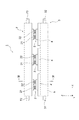
図1は第1実施形態に係る半導体装置を示す正面図、図2は図1に示す半導体装置の側面図である。図1および図2に示すように、本実施形態に係る半導体装置1は、3つの半導体モジュール2と、2つの冷却器3,7(第1冷却器3および第2冷却器7)とから構成されており、各半導体モジュール2を2つの冷却器3,7で挟み込むことにより、半導体装置1においては、半導体モジュール2を両面から冷却する両面冷却構造が採られている。   FIG. 1 is a front view showing the semiconductor device according to the first embodiment, and FIG. 2 is a side view of the semiconductor device shown in FIG. As shown in FIGS. 1 and 2, the semiconductor device 1 according to this embodiment includes three semiconductor modules 2 and two coolers 3 and 7 (first cooler 3 and second cooler 7). In addition, the semiconductor device 1 has a double-sided cooling structure that cools the semiconductor module 2 from both sides by sandwiching each semiconductor module 2 between the two coolers 3 and 7.

冷却器3,7による冷却対象物である半導体モジュール2は、三相インバータブリッジ回路を個別に構成するIGBT(Insulated Gate Bipolar Transistor)などのトランジスタやダイオードからなる半導体素子21,22を有している。これら半導体素子21,22の両主面には、はんだ付けにより形成されたはんだ層23,24を介して、一対の電極25,26が接続されている。また、半導体装置1を構成する各半導体モジュール2は、端子電極27,28に電気的に接続されており、端子電極27,28を介して、電力の入力/出力が可能となっている。なお、半導体モジュール2は、通電により発熱することから、以下に説明する冷却器3,7により、除熱が行われることとなる。また、半導体素子21,22は、IGBTなどのトランジスタやダイオードに限定されるものではなく、他の発熱素子であってもよい。   The semiconductor module 2 that is an object to be cooled by the coolers 3 and 7 includes semiconductor elements 21 and 22 made of transistors and diodes such as IGBTs (Insulated Gate Bipolar Transistors) that individually constitute a three-phase inverter bridge circuit. . A pair of electrodes 25 and 26 are connected to both main surfaces of these semiconductor elements 21 and 22 via solder layers 23 and 24 formed by soldering. In addition, each semiconductor module 2 constituting the semiconductor device 1 is electrically connected to the terminal electrodes 27 and 28, and power can be input / output via the terminal electrodes 27 and 28. In addition, since the semiconductor module 2 generates heat when energized, heat removal is performed by the coolers 3 and 7 described below. The semiconductor elements 21 and 22 are not limited to transistors and diodes such as IGBTs, and may be other heating elements.

第1冷却器3および第2冷却器7は、半導体モジュール2を冷却するための冷却器であり、図1に示すように、第1冷却器3は、各半導体モジュール2の下側に配置されており、第2冷却器7は、各半導体モジュール2の上側に配置されている。ここで、図3は、図2のIII-III線に沿う断面図である。   The first cooler 3 and the second cooler 7 are coolers for cooling the semiconductor module 2. As shown in FIG. 1, the first cooler 3 is disposed below each semiconductor module 2. The second cooler 7 is disposed on the upper side of each semiconductor module 2. Here, FIG. 3 is a cross-sectional view taken along line III-III in FIG.

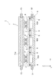
第1冷却器3は、図3に示すように、各半導体モジュール2に対応して設けられた3つの第1放熱体4に、単一の第2放熱体5を組み合わせて構成されており、これら第1放熱体4と第2放熱体5とが組み合わさることにより、内部に冷媒が流れるための流路(以下、冷媒流路。)が形成されている。そして、導入パイプ31から、第1冷却器3内に形成された冷媒流路内に冷媒が連続的に導入され、導入された冷媒が、X方向に沿って、この冷媒流路を流れることにより、各半導体モジュール2により発生した熱を放熱できるようになっている。なお、第1冷却器3内に導入された冷媒は、排出パイプ32から連続的に排出されることとなる。また、第1冷却器3を構成する各第1放熱体4および第2放熱体5は、例えば、熱伝導性の優れたアルミニウムやアルミニウム合金などを原材料として、ダイカストや押出し成型などにより、それぞれ個別に成型されてなるものである。   As shown in FIG. 3, the first cooler 3 is configured by combining a single second radiator 5 with the three first radiators 4 provided corresponding to the respective semiconductor modules 2. By combining the first heat radiating body 4 and the second heat radiating body 5, a flow path (hereinafter referred to as a refrigerant flow path) through which the refrigerant flows is formed. Then, the refrigerant is continuously introduced from the introduction pipe 31 into the refrigerant flow path formed in the first cooler 3, and the introduced refrigerant flows through the refrigerant flow path along the X direction. The heat generated by each semiconductor module 2 can be dissipated. In addition, the refrigerant introduced into the first cooler 3 is continuously discharged from the discharge pipe 32. The first radiator 4 and the second radiator 5 constituting the first cooler 3 are individually made by, for example, die casting or extrusion molding using aluminum or aluminum alloy having excellent thermal conductivity as a raw material. It is formed by molding.

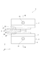
図4は、図1のIV-IV線に沿う断面図である。この図4中においては、第1冷却器3を構成する3つの第1放熱体4のうち、冷媒流路の最も上流側に配置された第1放熱体4を通る断面を示している。以下、3つの第1放熱体4のうち、冷媒流路の最も上流側に配置された第1放熱体4を例示して説明を行なうが、他の第1放熱体4も同様の構成を有するものである。第1放熱体4は、図4に示すように、一方の主面に、半導体モジュール2が配置され、半導体モジュール2から伝達された熱を受熱するような構成となっている。また、第1放熱体4は、他方の主面に、受熱した熱を放熱するための放熱部41と、放熱部41を周囲する第1嵌合部43とを有している。なお、第1嵌合部43は、後述する第2放熱体5の第2嵌合部52に嵌合するための部分である。   4 is a cross-sectional view taken along line IV-IV in FIG. In FIG. 4, the cross section which passes along the 1st heat radiator 4 arrange | positioned in the most upstream side of a refrigerant | coolant flow path among the three 1st heat radiators 4 which comprise the 1st cooler 3 is shown. Hereinafter, among the three first radiators 4, the first radiator 4 disposed on the most upstream side of the refrigerant flow path will be described as an example, but the other first radiators 4 have the same configuration. Is. As shown in FIG. 4, the first heat radiator 4 is configured such that the semiconductor module 2 is disposed on one main surface and receives heat transmitted from the semiconductor module 2. Moreover, the 1st heat radiator 4 has the thermal radiation part 41 for radiating the received heat and the 1st fitting part 43 surrounding the thermal radiation part 41 in the other main surface. In addition, the 1st fitting part 43 is a part for fitting in the 2nd fitting part 52 of the 2nd thermal radiation body 5 mentioned later.

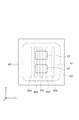
図5は、半導体素子21,22と放熱部41との位置関係を説明するための図であり、第1放熱体4をZ軸方向に沿って半導体モジュール2側から見た図である。なお、図5においては、半導体素子21,22を実線で、放熱フィン42a〜42eを破線で、放熱部41を一点鎖線で、それぞれ示している。図4、図5に示すように、放熱部41は、第2放熱体5側に向かって突出した複数の放熱フィン42a〜42eを有しており、これら複数の放熱フィン42a〜42eは、図4、図5に示すように、半導体素子21,22を中心として、Y方向に所定の間隔で配列されている。また、これら複数の放熱フィン42a〜42eは、図5に示すように、X方向(すなわち、冷媒の流れ方向)に沿って、連続的に延伸してなるものである。   FIG. 5 is a view for explaining the positional relationship between the semiconductor elements 21 and 22 and the heat radiating portion 41, and is a view of the first heat radiating body 4 viewed from the semiconductor module 2 side along the Z-axis direction. In FIG. 5, the semiconductor elements 21 and 22 are indicated by solid lines, the radiation fins 42 a to 42 e are indicated by broken lines, and the radiation part 41 is indicated by a one-dot chain line. As shown in FIGS. 4 and 5, the heat radiating portion 41 has a plurality of heat radiating fins 42 a to 42 e protruding toward the second heat radiating body 5, and the plurality of heat radiating fins 42 a to 42 e are shown in FIG. 4. As shown in FIG. 5, the semiconductor elements 21 and 22 are arranged at predetermined intervals in the Y direction. Further, as shown in FIG. 5, the plurality of heat radiation fins 42a to 42e are continuously extended along the X direction (that is, the refrigerant flow direction).

第1嵌合部43は、図4、図5に示すように、放熱部41を周囲している。第1嵌合部43は、シール部材6を介して、第2放熱体5の第2嵌合部53と嵌合されており、第1嵌合部43および第2嵌合部53を互いに嵌合することで、第1放熱体4と第2放熱体5とが組み合わされている。   As shown in FIGS. 4 and 5, the first fitting portion 43 surrounds the heat radiating portion 41. The first fitting portion 43 is fitted to the second fitting portion 53 of the second radiator 5 via the seal member 6, and the first fitting portion 43 and the second fitting portion 53 are fitted to each other. By combining, the first radiator 4 and the second radiator 5 are combined.

一方、第2放熱体5は、図4に示すように、第1放熱体4の放熱部41を受容する受容部51と、この受容部51を周囲する第2嵌合部53とを有している。図4に示すように、第2嵌合部53は、第1放熱体4の第1嵌合部43と、シール部材6を介して嵌合しており、これにより、受容部51は、図4に示すように、第1放熱体4の放熱部41(放熱フィン42a〜42eを含む)を受容しつつ、第1放熱体4の放熱部41とともに、冷媒流路を形成することとなる。   On the other hand, as shown in FIG. 4, the second heat radiating body 5 has a receiving portion 51 that receives the heat radiating portion 41 of the first heat radiating body 4 and a second fitting portion 53 that surrounds the receiving portion 51. ing. As shown in FIG. 4, the second fitting portion 53 is fitted to the first fitting portion 43 of the first radiator 4 via the seal member 6, whereby the receiving portion 51 is 4, the refrigerant flow path is formed together with the heat radiating portion 41 of the first heat radiating body 4 while receiving the heat radiating portion 41 (including the heat radiating fins 42a to 42e) of the first heat radiating body 4.

そして、第1放熱体と第2放熱体とを組み合わせて形成された冷媒流路内に、冷媒を流通させることで、冷媒流路内を流通する冷媒により、第1放熱体4が冷却され、これにより、半導体モジュール2が冷却されるようになっている。具体的には、半導体モジュール2で発生した熱は、半導体モジュール2が配置されている第1放熱体4により受熱され、第1放熱体4の放熱フィン42a〜42eに熱拡散し、拡散した熱が、冷媒流路内を流れる冷媒により、第1放熱体4の放熱フィン42a〜42eが冷却されることで、第1放熱体4に配置された半導体モジュール2が冷却されることとなる。   And the 1st heat radiating body 4 is cooled by the refrigerant | coolant which distribute | circulates the inside of a refrigerant | coolant flow path by distribute | circulating a refrigerant | coolant in the refrigerant | coolant flow path formed combining the 1st heat radiating body and the 2nd heat radiating body, Thereby, the semiconductor module 2 is cooled. Specifically, the heat generated in the semiconductor module 2 is received by the first heat radiating body 4 in which the semiconductor module 2 is disposed, thermally diffused to the heat radiating fins 42 a to 42 e of the first heat radiating body 4, and the diffused heat. However, the semiconductor module 2 disposed in the first heat radiator 4 is cooled by cooling the heat radiation fins 42a to 42e of the first heat radiator 4 by the refrigerant flowing in the refrigerant flow path.

また、第1放熱体4と第2放熱体5との間には、図4に示すように、シール部材6が介装されている。このシール部材6は、各嵌合部43,53により両側から押圧された状態で介装されており、これにより、各嵌合部43,53にそれぞれ密着し、冷媒流路をシールしている。なお、シール部材6としては、特に限定されないが、例えば、ゴム材料などの弾性体からなるシールリングなどを用いることができる。   Further, a seal member 6 is interposed between the first radiator 4 and the second radiator 5 as shown in FIG. The seal member 6 is interposed in a state of being pressed from both sides by the fitting portions 43 and 53, and thereby is in close contact with the fitting portions 43 and 53 to seal the refrigerant flow path. . The seal member 6 is not particularly limited. For example, a seal ring made of an elastic body such as a rubber material can be used.

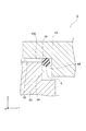
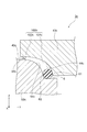
図6は、図4のVI部分における要部断面図であり、図4に示す第1放熱体4の第1嵌合部43と第2放熱体5の第2嵌合部53との嵌合部分を示している。第1嵌合部43と第2嵌合部53との間には、図6に示すように、シール部材6が介装されており、シール部材6を介して、第1嵌合部43と第2嵌合部53とが嵌合されている。   6 is a cross-sectional view of the main part in the VI portion of FIG. 4, and the fitting of the first fitting portion 43 of the first radiator 4 and the second fitting portion 53 of the second radiator 5 shown in FIG. 4. Shows the part. As shown in FIG. 6, a seal member 6 is interposed between the first fitting portion 43 and the second fitting portion 53, and the first fitting portion 43 and the first fitting portion 43 are interposed via the seal member 6. The second fitting portion 53 is fitted.

図6に示すように、第1嵌合部43には、高さhの段差形状が設けられており、また、第2嵌合部53には、高さhの段差形状が設けられている。そして、このように段差形状をそれぞれ有する第1嵌合部43および第2嵌合部53は、シール部材6を介して、嵌合されており、これにより、図6に示すように、第1嵌合部43と第2嵌合部53との間に、間隙100が形成されている。 As shown in FIG. 6, the first fitting portion 43 is provided with a step shape having a height h 1 , and the second fitting portion 53 is provided with a step shape having a height h 2. ing. And the 1st fitting part 43 and the 2nd fitting part 53 which each have a level | step difference in this way are fitted via the sealing member 6, Thereby, as shown in FIG. A gap 100 is formed between the fitting portion 43 and the second fitting portion 53.

この間隙100は、図6に示すように、シール部材6により冷媒流路から隔てられており、シール部材6を間にして、冷媒流路が形成されている側と異なる側に形成されている。また、この間隙100は、図6に示すように、第1冷却器3の外部に連通して形成されているため、シール部材6は、冷媒流路側の部分において、冷媒と接する一方で、冷媒流路とは異なる間隙100側の部分において、該間隙100を介して、外気と接することとなる。   As shown in FIG. 6, the gap 100 is separated from the refrigerant flow path by the seal member 6, and is formed on a side different from the side on which the refrigerant flow path is formed with the seal member 6 in between. . Further, as shown in FIG. 6, the gap 100 is formed so as to communicate with the outside of the first cooler 3, so that the seal member 6 is in contact with the refrigerant in the portion on the refrigerant flow path side. A portion on the gap 100 side that is different from the flow path is in contact with the outside air via the gap 100.

この間隙100は、図6に示すように、幅がwである第1部分101と、幅がwである第2部分102とを有している。第1部分101は、第1嵌合部43の対向面44と、第2嵌合部53の対向面54とが、幅wで対向することにより形成されている。また、図6に示すように、第1部分101は、第1嵌合部43の対向面44と第2嵌合部53の対向面54とにより、シール部材6を押圧することにより、幅wで形成されてなるものである。そのため、シール部材6の配置位置における第1嵌合部43と第2嵌合部53との間の幅も、幅wとなっている。 The gap 100, as shown in FIG. 6, has a first portion 101 a width of w 1, a second portion 102 a width of w 2. The first portion 101 includes a facing surface 44 of the first fitting portion 43, and the facing surface 54 of the second fitting portion 53 is formed by opposing a width w 1. Further, as shown in FIG. 6, the first portion 101 has a width w by pressing the seal member 6 with the facing surface 44 of the first fitting portion 43 and the facing surface 54 of the second fitting portion 53. 1 is formed. Therefore, the width between the first fitting portion 43 and the second fitting portion 53 at the arrangement position of the seal member 6 is also the width w 1 .

一方、第2部分102は、第1嵌合部43の対向面45と、第2嵌合部53の対向面55とが、幅wで対向することにより、形成されている。本実施形態においては、この第2部分102の幅wは、第1部分101の幅wよりも、幅が狭く形成されている。すなわち、図6中において、間隙100の幅は、w>wの関係となるように形成されている。 The second portion 102 includes a facing surface 45 of the first fitting portion 43, and the facing surface 55 of the second fitting portion 53 by opposing a width w 2, are formed. In the present embodiment, the width w 2 of the second portion 102 is narrower than the width w 1 of the first portion 101. That is, in FIG. 6, the width of the gap 100 is formed so as to satisfy the relationship of w 1 > w 2 .

以上のように、第1冷却器3は構成される。   As described above, the first cooler 3 is configured.

また、半導体装置1は、図3、図4に示すように、上述した第1冷却器3以外に、第2冷却器7を備えており、第2冷却器7は、複数の放熱フィン71a〜71eと、導入パイプ72と、排出パイプ73とを有している。第2冷却器7においても、第1冷却器3と同様に、冷媒が、連続的に、導入パイプ72から第2冷却器7の冷媒流路内へと導入され、これにより、半導体モジュール2を冷却するようになっている。   Further, as shown in FIGS. 3 and 4, the semiconductor device 1 includes a second cooler 7 in addition to the first cooler 3 described above, and the second cooler 7 includes a plurality of heat radiation fins 71 a to 71 a. 71e, an introduction pipe 72, and a discharge pipe 73. Also in the second cooler 7, as in the first cooler 3, the refrigerant is continuously introduced from the introduction pipe 72 into the refrigerant flow path of the second cooler 7. It is designed to cool.

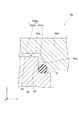
以上のように、本実施形態では、半導体モジュール2を冷却するための冷却器として、第1放熱体4と第2放熱体5とが組み合わされてなる第1冷却器3を有している。そして、この第1冷却器3においては、第1放熱体4の第1嵌合部43と第2放熱体5の第2嵌合部53との間には、間隙100が形成されており、この間隙100は、幅がwである第1部分101と、幅がwである第2部分102とを有し、この第2部分102の幅wが、第1部分101の幅wよりも、幅が狭く形成されている。これにより、シール部材6が劣化し、シール部材6のシール性能が低下した場合でも、劣化したシール部材6が、幅の狭い第2部分102において、冷媒流路を適切にシールすることができるため、冷媒の漏れを有効に防止することができる。具体的には、図6に示すように、シール部材6は、劣化していない初期状態においては、図6に示す位置において、第1嵌合部43と第2嵌合部53とにより挟持され、冷媒流路をシールしている。そして、図7に示すように、シール部材6が劣化し、シール部材6のシール性能が低下した場合でも、図7に示す位置において、冷媒流路をシールすることができる。すなわち、シール部材6のシール性能が低下した場合でも、第1部分101よりも狭い幅を有する第2部分102において、冷媒流路を適切にシールすることができる。すなわち、シール部材6の自封効果により、冷媒流路を適切にシールすることができる。ここで、図7は、第1実施形態に係る半導体装置1の作用効果を説明するための図であり、図7に示す断面は、図6に示す断面に相当するものである。 As described above, the present embodiment includes the first cooler 3 in which the first radiator 4 and the second radiator 5 are combined as a cooler for cooling the semiconductor module 2. In the first cooler 3, a gap 100 is formed between the first fitting portion 43 of the first radiator 4 and the second fitting portion 53 of the second radiator 5. the gap 100 has a first portion 101 a width of w 1, a second portion 102 width is w 2, a width w 2 of the second portion 102, the width w of the first portion 101 The width is narrower than 1 . Thereby, even when the sealing member 6 is deteriorated and the sealing performance of the sealing member 6 is deteriorated, the deteriorated sealing member 6 can appropriately seal the refrigerant flow path in the narrow second portion 102. The leakage of the refrigerant can be effectively prevented. Specifically, as shown in FIG. 6, the seal member 6 is sandwiched between the first fitting portion 43 and the second fitting portion 53 at the position shown in FIG. The refrigerant flow path is sealed. As shown in FIG. 7, even when the sealing member 6 is deteriorated and the sealing performance of the sealing member 6 is deteriorated, the refrigerant flow path can be sealed at the position shown in FIG. That is, even when the sealing performance of the sealing member 6 is deteriorated, the refrigerant flow path can be appropriately sealed in the second portion 102 having a narrower width than the first portion 101. That is, the refrigerant flow path can be properly sealed by the self-sealing effect of the seal member 6. Here, FIG. 7 is a view for explaining the function and effect of the semiconductor device 1 according to the first embodiment, and the cross section shown in FIG. 7 corresponds to the cross section shown in FIG.

すなわち、図6に示す初期状態においては、シール部材6は、第1嵌合部43の対向面44と第2嵌合部53の対向面54とにより両側から押圧されており、第1嵌合部43および第2嵌合部53に密着している。そのため、シール部材6は、図6に示す位置で、第1嵌合部43と第2嵌合部53とにより挟持され、冷媒流路をシールしている。   That is, in the initial state shown in FIG. 6, the seal member 6 is pressed from both sides by the facing surface 44 of the first fitting portion 43 and the facing surface 54 of the second fitting portion 53. The part 43 and the second fitting part 53 are in close contact with each other. Therefore, the seal member 6 is sandwiched between the first fitting portion 43 and the second fitting portion 53 at the position shown in FIG. 6 to seal the refrigerant flow path.

一方、シール部材6が劣化し、シール部材6の弾性力の低下や、シール部材6の変形などにより、シール部材6のシール性能が低下した場合、シール部材6と第1嵌合部43との間、および、シール部材6と第2嵌合部53との間の密着力は小さくなる。ここで、シール部材6は、上述したように、冷媒流路側において、冷媒流路内を流れる冷媒と接しており、冷媒の圧力により、間隙100側へと押圧されている一方、シール部材6は、間隙100側において、間隙を介して、外気と接しており、外気からの圧力により、冷媒流路側へと押圧されている。通常、冷媒の圧力は外気の圧力よりも大きく、シール部材6には、間隙側に押し上げる押圧力がより大きく掛かることとなる。そのため、シール部材6が劣化し、シール部材6のシール性能が低下した場合、シール部材6は、冷媒の押圧力に耐え切れず、図7に示すように、間隙100側に向かって、図7に示す位置まで、押し上げられることとなる。   On the other hand, when the sealing member 6 is deteriorated and the sealing performance of the sealing member 6 is deteriorated due to a decrease in elastic force of the sealing member 6 or deformation of the sealing member 6, the sealing member 6 and the first fitting portion 43 are The contact force between the sealing member 6 and the second fitting portion 53 becomes small. Here, as described above, the seal member 6 is in contact with the refrigerant flowing in the refrigerant channel on the refrigerant channel side, and is pressed toward the gap 100 by the pressure of the refrigerant, while the seal member 6 is The gap 100 is in contact with the outside air through the gap and is pressed toward the refrigerant flow path by the pressure from the outside air. Normally, the pressure of the refrigerant is larger than the pressure of the outside air, and the pressing force that pushes up toward the gap is applied to the seal member 6 more. Therefore, when the sealing member 6 deteriorates and the sealing performance of the sealing member 6 decreases, the sealing member 6 cannot withstand the pressing force of the refrigerant, and as shown in FIG. Will be pushed up to the position shown in FIG.

ここで、上述したように、第1嵌合部43と第2嵌合部53との間に形成された間隙100は、幅がwである第1部分101と、幅がwである第2部分102とを有しており、第2部分の幅wは、第1部分の幅wよりも、幅が狭く形成されている。そのため、本実施形態によれば、冷媒の圧力により間隙100側に押し上げられたシール部材6は、図7に示す位置に移動し、図7に示す位置において、冷媒流路を適切にシールすることができ、これにより、冷媒流路からの冷媒の漏出を有効に防止することができる。 Here, as described above, the gap 100 formed between the first fitting portion 43 and the second fitting portion 53 has the first portion 101 having the width w 1 and the width w 2 . and a second portion 102, the width w 2 of the second portion is greater than the width w 1 of the first portion, is formed narrower. Therefore, according to this embodiment, the seal member 6 pushed up to the gap 100 side by the pressure of the refrigerant moves to the position shown in FIG. 7, and appropriately seals the refrigerant flow path at the position shown in FIG. Thus, leakage of the refrigerant from the refrigerant channel can be effectively prevented.

≪第2実施形態≫
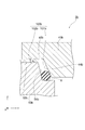
続いて、本発明の第2実施形態について説明する。図8は、第2実施形態に係る第1冷却器3aの断面図であり、図4のIV部分に相当する部分における要部断面図である。第2実施形態においては、第1冷却器3aが、以下に説明する点において、第1実施形態の第1冷却器3と異なる以外は、上述の第1実施形態と同様の構成と作用を有し、その重複する説明は省略する。
<< Second Embodiment >>
Subsequently, a second embodiment of the present invention will be described. FIG. 8 is a cross-sectional view of the first cooler 3a according to the second embodiment, and is a main-portion cross-sectional view of a portion corresponding to the IV portion of FIG. In the second embodiment, the first cooler 3a has the same configuration and operation as those of the first embodiment except that the first cooler 3a is different from the first cooler 3 of the first embodiment in the points described below. The overlapping description is omitted.

図8に示すように、第1冷却器3aは、第1放熱体4aの第1嵌合部43aに、第2放熱体5の対向面54に対向するテーパー面44aが形成されており、この点において、第1実施形態に係る第1冷却器3と異なる。なお、このテーパー面44aは、例えば、個別成型した第1放熱体の嵌合部を、切削加工することにより設けることができる。   As shown in FIG. 8, in the first cooler 3a, a tapered surface 44a facing the facing surface 54 of the second radiator 5 is formed in the first fitting portion 43a of the first radiator 4a. In the point, it differs from the 1st cooler 3 concerning a 1st embodiment. In addition, this taper surface 44a can be provided by cutting the fitting part of the 1st thermal radiation body shape | molded separately, for example.

そして、テーパー面44aが設けられた第1嵌合部43aと、段差形状が設けられた第2嵌合部53とは、シール部材6を介して、嵌合されており、これにより、図8に示すように、第1嵌合部43aと第2嵌合部53との間に、間隙100aが形成されている。   And the 1st fitting part 43a provided with the taper surface 44a and the 2nd fitting part 53 provided with the level | step difference shape are fitted via the seal member 6, and, thereby, FIG. As shown, a gap 100 a is formed between the first fitting portion 43 a and the second fitting portion 53.

この間隙100aは、図8に示すように、シール部材6の配置位置から遠いほど、幅が連続的に狭くなる第1部分101aと、幅がwである第2部分102aとを有している。 As shown in FIG. 8, the gap 100 a includes a first portion 101 a having a width that continuously decreases as the distance from the arrangement position of the seal member 6, and a second portion 102 a having a width w 2. Yes.

第1部分101aは、第1嵌合部43aのテーパー面44aと、第2嵌合部53の対向面54との間に形成される間隙であり、第1部分101aは、図8に示すように、テーパー面44aが対向面54に対して傾いて形成されているため、第1部分101aの幅は、シール部材6の配置位置から遠くなるほど、連続的に狭くなっている。すなわち、図8に示すように、第1部分101aは、シール部材6の配置位置付近において、その幅が最も広くなるように形成されている。   The first portion 101a is a gap formed between the tapered surface 44a of the first fitting portion 43a and the facing surface 54 of the second fitting portion 53, and the first portion 101a is as shown in FIG. In addition, since the tapered surface 44 a is formed to be inclined with respect to the opposing surface 54, the width of the first portion 101 a is continuously narrower as the distance from the position where the seal member 6 is disposed. That is, as shown in FIG. 8, the first portion 101 a is formed to have the widest width in the vicinity of the arrangement position of the seal member 6.

一方、第2部分102aは、第1嵌合部43aの対向面45aと、第2嵌合部53の対向面55とが、幅wで対向することにより、形成されている。本実施形態においては、この第2部分102aの幅wは、第1部分101aの幅よりも、幅が狭く形成されている。 On the other hand, the second portion 102a is opposed surface 45a of the first fitting portion 43a, and the opposing surface 55 of the second fitting portion 53 by opposing a width w 2, it is formed. In the present embodiment, the width w 2 of the second portion 102a is greater than the width of the first portion 101a, and is formed narrower.

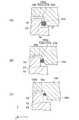
以上のように、第2実施形態では、第1嵌合部43aにテーパー面44aが設けられており、テーパー面44aを有する第1嵌合部と、段差形状を有する第2嵌合部53との間に、間隙100aが形成されている。そして、この間隙100aは、第1部分101aと、第2部分102aとを有しており、この第1部分101aは、シール部材6の配置位置から遠くなるほど、幅が連続的に狭く形成されている。これにより、第1冷却器3aでは、シール部材6が劣化し、シール部材6のシール性能が低下した場合でも、劣化したシール部材6が、第1部分中のシール部材6の劣化度合いに応じた位置において、冷媒流路を連続的にシールすることができるため、冷媒流路からの冷媒の漏出をより有効に防止することができる。すなわち、シール部材6の自封効果を持続することができるため、冷媒流路からの冷媒の漏出をより有効に防止することができる。   As described above, in the second embodiment, the first fitting portion 43a is provided with the tapered surface 44a, the first fitting portion having the tapered surface 44a, and the second fitting portion 53 having a step shape. A gap 100a is formed between the two. And this gap | interval 100a has the 1st part 101a and the 2nd part 102a, and this 1st part 101a is formed so that a width | variety is continuously narrowed, so that it is far from the arrangement position of the sealing member 6. Yes. Thereby, in the 1st cooler 3a, even when the sealing member 6 deteriorates and the sealing performance of the sealing member 6 deteriorates, the deteriorated sealing member 6 corresponds to the degree of deterioration of the sealing member 6 in the first portion. Since the refrigerant flow path can be continuously sealed at the position, leakage of the refrigerant from the refrigerant flow path can be more effectively prevented. That is, since the self-sealing effect of the seal member 6 can be maintained, leakage of the refrigerant from the refrigerant flow path can be more effectively prevented.

具体的には、シール部材6は、劣化していない初期状態においては、図8に示す位置で、第1嵌合部43aと第2嵌合部53とにより挟持され、冷媒流路をシールしている。そして、シール部材6が劣化し、シール部材6のシール性能が低下した場合、冷媒の圧力により、間隙100a側に向かって、徐々に押し上げられていくこととなる。   Specifically, in the initial state where the seal member 6 is not deteriorated, the seal member 6 is sandwiched between the first fitting portion 43a and the second fitting portion 53 at the position shown in FIG. ing. When the sealing member 6 is deteriorated and the sealing performance of the sealing member 6 is deteriorated, the sealing member 6 is gradually pushed up toward the gap 100a by the pressure of the refrigerant.

ここで、上述したように、第1嵌合部43aと第2嵌合部53との間に形成された間隙100aは、テーパー面44aと対向面54との間に形成された第1部分101aを有しており、この第1部分101aは、シール部材6の配置位置から遠くなるほど、連続的に幅が狭く形成されている。そのため、シール部材6が劣化すると、シール部材6は、劣化度合いに応じて、徐々に間隙100a側に移動し、例えば、図9(A)に示す位置で、第1嵌合部43aと第2嵌合部53とに挟持され、冷媒流路をシールする。   Here, as described above, the gap 100a formed between the first fitting portion 43a and the second fitting portion 53 is the first portion 101a formed between the tapered surface 44a and the facing surface 54. The first portion 101a is formed to have a continuously narrower width as it is farther from the position where the seal member 6 is disposed. Therefore, when the seal member 6 deteriorates, the seal member 6 gradually moves to the gap 100a side according to the degree of deterioration, and, for example, at the position shown in FIG. It is pinched by the fitting part 53 and seals the refrigerant flow path.

そして、同様に、シール部材6がさらに劣化していくと、シール部材6は、劣化度合いに応じて、徐々に間隙100a側に移動し、例えば、図9(A)に示す位置よりさらに幅の狭い図9(B)に示す位置で冷媒流路をシールし、その後、さらにシール部材6が劣化した場合には、例えば、図9(B)に示す位置よりさらに幅の狭い図9(C)に示す位置で、冷媒流路をシールする。このように、第2実施形態に係る第1冷却器3aでは、シール部材6が劣化し、シール部材6のシール性能が低下した場合でも、シール部材6は、シール部材6の劣化度合いに応じて、冷媒流路を連続的にシールすることができるため、冷媒流路からの冷媒の漏出をより有効に防止することができる。なお、図9は、第2実施形態に係る半導体装置の作用効果を説明するための図であり、図9は、図8に示す断面に相当する断面における断面図である。   Similarly, when the seal member 6 further deteriorates, the seal member 6 gradually moves to the gap 100a side according to the degree of deterioration, and is, for example, wider than the position shown in FIG. When the refrigerant flow path is sealed at the narrow position shown in FIG. 9B and then the seal member 6 is further deteriorated, for example, the width shown in FIG. 9C is narrower than that shown in FIG. 9B. The refrigerant flow path is sealed at the position shown in FIG. As described above, in the first cooler 3a according to the second embodiment, even when the sealing member 6 is deteriorated and the sealing performance of the sealing member 6 is deteriorated, the sealing member 6 depends on the degree of deterioration of the sealing member 6. Since the refrigerant flow path can be continuously sealed, leakage of the refrigerant from the refrigerant flow path can be more effectively prevented. FIG. 9 is a diagram for explaining the function and effect of the semiconductor device according to the second embodiment. FIG. 9 is a cross-sectional view corresponding to the cross section shown in FIG.

≪第3実施形態≫
続いて、本発明の第3実施形態について説明する。図10は、第3実施形態に係る第1冷却器3bの断面図であり、図4のIV部分に相当する要部断面図である。第3実施形態においては、第1冷却器3bが、以下に説明する点において、第1実施形態の第1冷却器3と異なる以外は、上述の第1実施形態と同様の構成と作用を有し、その重複する説明は省略する。
«Third embodiment»
Subsequently, a third embodiment of the present invention will be described. FIG. 10 is a cross-sectional view of the first cooler 3b according to the third embodiment, and is a main-portion cross-sectional view corresponding to the IV portion of FIG. In 3rd Embodiment, it has the structure and effect | action similar to the above-mentioned 1st Embodiment except the 1st cooler 3b differing from the 1st cooler 3 of 1st Embodiment in the point demonstrated below. The overlapping description is omitted.

図10に示すように、第1冷却器3bは、第1放熱体4bの第1嵌合部43bにテーパー面44bが、第2放熱体5bの第2嵌合部53bに、テーパー面44bに対向するテーパー面54bが、それぞれ形成されており、これらの点において、第1実施形態に係る第1冷却器3と異なる。なお、テーパー面43bおよびテーパー面54bは、例えば、個別成型した各放熱体の嵌合部を、切削加工することにより設けることができる。   As shown in FIG. 10, the first cooler 3b has a tapered surface 44b on the first fitting portion 43b of the first radiator 4b, a second fitting portion 53b on the second radiator 5b, and a tapered surface 44b. Opposing tapered surfaces 54b are formed, respectively, and differ from the first cooler 3 according to the first embodiment in these points. In addition, the taper surface 43b and the taper surface 54b can be provided by cutting the fitting part of each heat-radiating body separately molded, for example.

そして、テーパー面44bが設けられた第1嵌合部43bと、テーパー面54bが設けられた第2嵌合部53bとは、シール部材6を介して、嵌合されており、図10に示すように、第1嵌合部43bと第2嵌合部53bとの間に、間隙100bが形成されている。   And the 1st fitting part 43b in which the taper surface 44b was provided, and the 2nd fitting part 53b in which the taper surface 54b was provided are fitted via the seal member 6, and are shown in FIG. As described above, the gap 100b is formed between the first fitting portion 43b and the second fitting portion 53b.

この間隙100bは、図10に示すように、シール部材6の配置位置から遠いほど、幅が連続的に狭くなる第1部分101bと、幅がwである第2部分102bとを有している。 The gap 100b, as shown in FIG. 10, farther from the position of the sealing member 6, has a width continuously narrower first portion 101b, and a second portion 102b width is w 2 Yes.

第1部分101bは、第1嵌合部43bのテーパー面44bと、第2嵌合部54bのテーパー面54bとの間に形成される間隙であり、第1部分101bは、図10に示すように、テーパー面44bの傾斜角度とテーパー面54bの傾斜角度とが互いに異なるため、シール部材6の配置位置から遠くなるほど、その幅が連続的に狭くなっている。すなわち、図10に示すように、第1部分101bは、シール部材6の配置位置付近において、その幅が最も広くなるように形成されている。   The first portion 101b is a gap formed between the tapered surface 44b of the first fitting portion 43b and the tapered surface 54b of the second fitting portion 54b. The first portion 101b is as shown in FIG. In addition, since the inclination angle of the taper surface 44b and the inclination angle of the taper surface 54b are different from each other, the width of the taper surface 44b becomes narrower as the distance from the arrangement position of the seal member 6 increases. That is, as shown in FIG. 10, the first portion 101 b is formed to have the widest width in the vicinity of the arrangement position of the seal member 6.

一方、第2部分102bは、第1嵌合部43bの対向面45bと、第2嵌合部53bの対向面55bとが、幅wで対向することにより、形成されている。本実施形態においては、この第2部分102bの幅wは、第1部分101bの幅よりも、幅が狭く形成されている。 The second portion 102b is opposed surface 45b of the first fitting portion 43 b, and the opposing surface 55b of the second fitting portion 53b is, by opposing a width w 2, it is formed. In the present embodiment, the width w 2 of the second portion 102b is greater than the width of the first portion 101b, is formed narrower.

以上のように、第3実施形態では、第1嵌合部43bにテーパー面44bが、第2嵌合部53bにテーパー面54bがそれぞれ設けられており、テーパー面44bを有する第1嵌合部43bとテーパー面54bを有する第2嵌合部53bとの間に、間隙100bが形成されている。そして、この間隙100bは、第1部分101bと、第2部分102bとを有しており、この第1部分101bは、シール部材6の配置位置から遠くなるほど、幅が連続的に狭く形成されている。これにより、第3実施形態に係る第1冷却器3bでは、第2実施形態に係る第1冷却器3aと同様に、シール部材6が劣化し、シール部材6のシール性能が低下した場合でも、シール部材6が、シール部材6の劣化度合いに応じた位置において、冷媒流路をより適切にシールすることができるため、冷媒流路からの冷媒の漏出をより有効に防止することができる。すなわち、シール部材6の自封効果を持続することができるため、冷媒流路からの冷媒の漏出をより有効に防止することができる。   As described above, in the third embodiment, the first fitting portion 43b is provided with the tapered surface 44b, the second fitting portion 53b is provided with the tapered surface 54b, and the first fitting portion having the tapered surface 44b. A gap 100b is formed between 43b and the second fitting portion 53b having the tapered surface 54b. The gap 100b includes a first portion 101b and a second portion 102b. The first portion 101b is formed so as to be continuously narrower as the distance from the arrangement position of the seal member 6 increases. Yes. Thereby, in the 1st cooler 3b concerning a 3rd embodiment, like the 1st cooler 3a concerning a 2nd embodiment, even when the seal member 6 deteriorates and the seal performance of the seal member 6 falls, Since the seal member 6 can more appropriately seal the refrigerant flow path at a position corresponding to the degree of deterioration of the seal member 6, leakage of the refrigerant from the refrigerant flow path can be more effectively prevented. That is, since the self-sealing effect of the seal member 6 can be maintained, leakage of the refrigerant from the refrigerant flow path can be more effectively prevented.

≪第4実施形態≫
続いて、本発明の第4実施形態について説明する。図11は、第4実施形態に係る第1冷却器3cの断面図であり、図4のIV部分に相当する要部断面図である。第4実施形態においては、第1冷却器3cが、以下に説明する点において、第1実施形態の第1冷却器3と異なる以外は、上述の第1実施形態と同様の構成と作用を有し、その重複する説明は省略する。
<< Fourth Embodiment >>
Subsequently, a fourth embodiment of the present invention will be described. FIG. 11 is a cross-sectional view of the first cooler 3c according to the fourth embodiment, and is a main-portion cross-sectional view corresponding to the IV portion of FIG. In the fourth embodiment, the first cooler 3c has the same configuration and operation as those of the first embodiment except that the first cooler 3c is different from the first cooler 3 of the first embodiment in the points described below. The overlapping description is omitted.

図11に示すように、第1冷却器3cにおいては、第1放熱体4cの第1嵌合部43cに凹曲面44cが、第2放熱体5cの第2嵌合部53cに凸曲面54cが、それぞれ形成されており、第1冷却器3cは、この点において、第1実施形態の第1冷却器3と異なる。なお、この凹曲面44cと凸曲面54cとは、図11に示すように、互いに異なる曲面形状に形成されている。   As shown in FIG. 11, in the first cooler 3c, a concave curved surface 44c is formed in the first fitting portion 43c of the first radiator 4c, and a convex curved surface 54c is formed in the second fitting portion 53c of the second radiator 5c. In this respect, the first cooler 3c is different from the first cooler 3 of the first embodiment. The concave curved surface 44c and the convex curved surface 54c are formed in different curved shapes as shown in FIG.

そして、凹曲面44cが設けられた第1嵌合部43cと、凸曲面54cが設けられた第2嵌合部53cとは、シール部材6を介して、嵌合されており、これにより、図11に示すように、第1嵌合部43cと第2嵌合部53cとの間に、間隙100cが形成されている。   And the 1st fitting part 43c in which the concave curved surface 44c was provided, and the 2nd fitting part 53c in which the convex curved surface 54c were provided are fitted via the seal member 6, and, thereby, FIG. 11, a gap 100c is formed between the first fitting portion 43c and the second fitting portion 53c.

この間隙100cは、図11に示すように、シール部材6から遠いほど、幅が連続的に狭くなる第1部分101cと、幅がwである第2部分101cとを有している。 The gap 100c, as shown in FIG. 11, farther from the sealing member 6 has a width continuously narrower first portion 101c, and a second portion 101c width of w 2.

第1部分101cは、第1嵌合部43cの凹曲面44cと、第2嵌合部53cの凸曲面54cとの間に形成される間隙であり、第1部分101cの幅は、シール部材6の配置位置から遠くなるほど、連続的に狭くなっている。すなわち、図11に示すように、第1部分101cは、シール部材6の配置位置付近において、その幅が最も広くなるように形成されている。   The first portion 101c is a gap formed between the concave curved surface 44c of the first fitting portion 43c and the convex curved surface 54c of the second fitting portion 53c, and the width of the first portion 101c is the sealing member 6. The farther away from the arrangement position, the narrower it becomes continuously. That is, as shown in FIG. 11, the first portion 101 c is formed to have the widest width in the vicinity of the arrangement position of the seal member 6.

一方、第2部分102cは、第1嵌合部43cの対向面45cと、第2嵌合部53cの対向面55cとが、幅wで対向することにより、形成されている。本実施形態においては、この第2部分102cの幅wは、第1部分101cの幅よりも、幅が狭く形成されている。 The second portion 102c is opposed surface 45c of the first engaging portion 43c, and the opposing surface 55c of the second engagement portion 53c is, by opposing a width w 2, it is formed. In the present embodiment, the width w 2 of the second portion 102c is greater than the width of the first portion 101c, and is formed narrower.

以上のように、第4実施形態では、第1嵌合部43cに凹曲面44cが、第2嵌合部53cに凸曲面54cがそれぞれ設けられており、凹曲面44cが形成された第1嵌合部43cと、凸曲面54cが形成された第2嵌合部53cとの間に、間隙100cが形成されている。そして、この間隙100cは、第1部分101cと、第2部分102cとを有しており、これらのうち、第1部分101cは、シール部材6の配置位置から遠くなるほど、幅が連続的に狭く形成されている。これにより、第4実施形態においては、シール部材6が劣化し、シール部材6のシール性能が低下した場合でも、シール部材6が、第1部分101c中のシール部材6の劣化度合いに応じた位置において、冷媒流路を連続的にシールすることができるため、冷媒流路からの冷媒の漏出をより有効に防止することができる。すなわち、シール部材6の自封効果を持続することができるため、冷媒流路からの冷媒の漏出をより有効に防止することができる。   As described above, in the fourth embodiment, the first fitting portion 43c is provided with the concave curved surface 44c, the second fitting portion 53c is provided with the convex curved surface 54c, and the first fitting is formed with the concave curved surface 44c. A gap 100c is formed between the joint portion 43c and the second fitting portion 53c in which the convex curved surface 54c is formed. And this gap | interval 100c has the 1st part 101c and the 2nd part 102c, The width | variety of the 1st part 101c is narrow continuously, so that it is far from the arrangement position of the sealing member 6 among these. Is formed. Thereby, in 4th Embodiment, even when the sealing member 6 deteriorates and the sealing performance of the sealing member 6 falls, the sealing member 6 is a position according to the deterioration degree of the sealing member 6 in the 1st part 101c. Since the refrigerant flow path can be continuously sealed, leakage of the refrigerant from the refrigerant flow path can be more effectively prevented. That is, since the self-sealing effect of the seal member 6 can be maintained, leakage of the refrigerant from the refrigerant flow path can be more effectively prevented.

具体的には、シール部材6は、劣化していない初期状態においては、図11に示す位置で、第1嵌合部43cと第2嵌合部53cとにより挟持され、冷媒流路をシールしている。そして、シール部材6が劣化し、シール部材6のシール性能が低下した場合には、シール部材6は、冷媒の圧力により、間隙100c側に向かって、徐々に押し上げられていくこととなる。   Specifically, the seal member 6 is sandwiched between the first fitting portion 43c and the second fitting portion 53c at the position shown in FIG. ing. When the sealing member 6 is deteriorated and the sealing performance of the sealing member 6 is deteriorated, the sealing member 6 is gradually pushed up toward the gap 100c by the pressure of the refrigerant.

ここで、上述したように、第1部分101cは、シール部材6の配置位置から遠くなるほど、連続的に幅が狭く形成されている。そのため、シール部材6が劣化すると、シール部材6は、劣化度合いに応じて、徐々に間隙100a側に移動し、例えば、図12(A)に示す位置で、第1嵌合部43cと第2嵌合部53cとにより挟持され、冷媒流路をシールする。   Here, as described above, the width of the first portion 101c is continuously narrowed as the distance from the arrangement position of the seal member 6 increases. Therefore, when the seal member 6 deteriorates, the seal member 6 gradually moves to the gap 100a side according to the degree of deterioration. For example, at the position shown in FIG. It is pinched by the fitting part 53c and seals the refrigerant flow path.

そして、同様に、シール部材6がさらに劣化していくと、シール部材6は、劣化度合いに応じて、徐々に間隙100a側に移動し、例えば、図12(A)に示す位置よりもさらに幅の狭い図12(B)に示す位置で冷媒流路をシールし、その後、さらにシール部材6が劣化した場合には、例えば、図12(B)よりもさらに幅が狭い図12(C)に示す位置で冷媒流路をシールし、さらにシール部材が劣化した場合には、例えば、図12(C)よりもさらに幅が狭い図12(D)に示す位置で、冷媒流路をシールする。このように、第4実施形態に係る第1冷却器3cでは、シール部材6が劣化し、シール部材6のシール性能が低下した場合でも、シール部材6は、シール部材6の劣化度合いに応じた位置において、冷媒流路を連続的にシールすることができるため、冷媒流路からの冷媒の漏出をより有効に防止することができる。なお、図12は、第4実施形態に係る半導体装置の作用効果を説明するための図であり、図12は、図11に示す断面に相当する断面における断面図である。   Similarly, when the seal member 6 further deteriorates, the seal member 6 gradually moves to the gap 100a side according to the degree of deterioration, and is, for example, wider than the position shown in FIG. When the refrigerant flow path is sealed at a narrow position shown in FIG. 12B and the seal member 6 is further deteriorated, for example, the width shown in FIG. 12C is narrower than that in FIG. When the refrigerant flow path is sealed at the position shown and the seal member is further deteriorated, for example, the refrigerant flow path is sealed at the position shown in FIG. 12D, which is narrower than FIG. 12C. Thus, in the first cooler 3c according to the fourth embodiment, even when the sealing member 6 is deteriorated and the sealing performance of the sealing member 6 is deteriorated, the sealing member 6 is in accordance with the degree of deterioration of the sealing member 6. Since the refrigerant flow path can be continuously sealed at the position, leakage of the refrigerant from the refrigerant flow path can be more effectively prevented. FIG. 12 is a view for explaining the function and effect of the semiconductor device according to the fourth embodiment. FIG. 12 is a cross-sectional view corresponding to the cross section shown in FIG.

さらに、本実施形態では、シール部材6と接する第1嵌合部43cの凹曲面44c、およびシール部材6と接する第2嵌合部53cの凸曲面54cは、いずれも曲面形状となっているため、シール部材6の凹曲面44cとの接点、およびシール部材6の凸曲面54cとの接点は、第1部分101c中のシール部材6の位置に応じて、徐々に変化していくこととなる。   Furthermore, in this embodiment, the concave curved surface 44c of the first fitting portion 43c that contacts the seal member 6 and the convex curved surface 54c of the second fitting portion 53c that contacts the seal member 6 are both curved surfaces. The contact point of the seal member 6 with the concave curved surface 44c and the contact point of the seal member 6 with the convex curved surface 54c gradually change according to the position of the seal member 6 in the first portion 101c.

例えば、図11および図12に示すシール部材6を例示して説明すると、図11に示す初期状態では、シール部材6は、凹曲面44cおよび凸曲面54cと、それぞれ接点61,62で接している。一方、シール部材6は、図12(A)に示す位置では、図11に示す接点61,62とは異なる接点61a,62aで、それぞれ凹曲面44cおよび凸曲面54cと接することとなる。同様に、シール部材6は、図12(B)〜(D)に示す位置では、それぞれ異なる接点、すなわち、接点61b,62b(図12(B))、接点61c,62c(図12(C))、接点61d,62d(図12(D))にて、凹曲面44cおよび凸曲面54cと接することとなる。   For example, the seal member 6 shown in FIGS. 11 and 12 will be described as an example. In the initial state shown in FIG. 11, the seal member 6 is in contact with the concave curved surface 44c and the convex curved surface 54c through the contacts 61 and 62, respectively. . On the other hand, at the position shown in FIG. 12A, the seal member 6 comes into contact with the concave curved surface 44c and the convex curved surface 54c at the contact points 61a and 62a different from the contact points 61 and 62 shown in FIG. Similarly, the seal member 6 has different contacts at the positions shown in FIGS. 12B to 12D, that is, the contacts 61b and 62b (FIG. 12B) and the contacts 61c and 62c (FIG. 12C). ), The contact points 61d and 62d (FIG. 12D) are in contact with the concave curved surface 44c and the convex curved surface 54c.

このように、シール部材と凹曲面44cとの接点、シール部材6と凸曲面54cとの接点は、第1部分101c中のシール部材6の位置に応じて、連続的に変化している。そのため、例えば、図11においては、シール部材6と凹曲面44cとの接点61、およびシール部材6と凸曲面54cとの接点62は、略Y方向に沿った線上に位置しているのに対し、シール部材6が間隙100c側に徐々に押し上げられていくと、シール部材6と凹曲面44cとの接点、およびシール部材6と凸曲面54cとの接点は、反時計回りに、徐々に変化していき、図12(D)においては、シール部材6と凹曲面44cとの接点61d、およびシール部材6と凸曲面54cとの接点62dは、略Z方向に沿った線上に位置することとなる。   Thus, the contact point between the seal member and the concave curved surface 44c and the contact point between the seal member 6 and the convex curved surface 54c are continuously changed according to the position of the seal member 6 in the first portion 101c. Therefore, for example, in FIG. 11, the contact 61 between the seal member 6 and the concave curved surface 44c and the contact 62 between the seal member 6 and the convex curved surface 54c are positioned on a line substantially along the Y direction. As the seal member 6 is gradually pushed up toward the gap 100c, the contact between the seal member 6 and the concave curved surface 44c and the contact between the seal member 6 and the convex curved surface 54c gradually change counterclockwise. In FIG. 12D, the contact 61d between the seal member 6 and the concave curved surface 44c and the contact 62d between the seal member 6 and the convex curved surface 54c are positioned on a line substantially along the Z direction. .

このように、シール部材6が劣化し、シール部材6が間隙100c側に押し上げられていくと、シール部材6の凹曲面44cとの接点、およびシール部材6の凸曲面54cとの接点は、第1部分101c中のシール部材6の位置に応じて、連続的に変化していくこととなるため、シール部材6の劣化を有効に抑制することができ、シール部材6のシール性能をより持続させることができる。   As described above, when the seal member 6 deteriorates and the seal member 6 is pushed up toward the gap 100c, the contact with the concave curved surface 44c of the seal member 6 and the contact with the convex curved surface 54c of the seal member 6 are Since it will change continuously according to the position of the sealing member 6 in 1 part 101c, deterioration of the sealing member 6 can be suppressed effectively and the sealing performance of the sealing member 6 is maintained more. be able to.

なお、以上説明した実施形態は、本発明の理解を容易にするために記載されたものであって、本発明を限定するために記載されたものではない。したがって、上記の実施形態に開示された各要素は、本発明の技術的範囲に属する全ての設計変更や均等物をも含む趣旨である。   The embodiment described above is described for facilitating the understanding of the present invention, and is not described for limiting the present invention. Therefore, each element disclosed in the above embodiment is intended to include all design changes and equivalents belonging to the technical scope of the present invention.

例えば、上述した実施形態においては、3つの半導体モジュール2を、2つの冷却器3,7で冷却する半導体装置1を例示したが、半導体装置1が備える半導体モジュールの数は特に限定されず、例えば、インバータ装置に用いられる半導体装置においては、6つの半導体モジュールを備える構成としてもよい。あるいは、単一の半導体モジュールを冷却器3,7で冷却する構成としてもよく、その場合には、第1冷却器3を、単一の第1放熱体と単一の第2放熱体とを組み合わせてなるものとすることができる。   For example, in the above-described embodiment, the semiconductor device 1 that cools the three semiconductor modules 2 with the two coolers 3 and 7 is illustrated, but the number of semiconductor modules included in the semiconductor device 1 is not particularly limited. The semiconductor device used for the inverter device may have six semiconductor modules. Or it is good also as a structure which cools a single semiconductor module with the coolers 3 and 7, and in that case, the 1st cooler 3 is made into a single 1st heat radiator and a single 2nd heat radiator. It can be a combination.

また、上述した実施形態では、第1冷却器3と第2冷却器7とを半導体モジュール2の両主面に配置し、半導体モジュール2を両側から冷却する半導体装置1を例示したが、半導体装置1の構成はこれに限定されず、例えば、第2冷却器7を第1冷却器3と同様の構成としてもよいし、または、半導体モジュール2の片面のみを単一の第1冷却器3で冷却する構成としてもよい。   In the above-described embodiment, the semiconductor device 1 is exemplified in which the first cooler 3 and the second cooler 7 are arranged on both main surfaces of the semiconductor module 2 and the semiconductor module 2 is cooled from both sides. The configuration of 1 is not limited to this. For example, the second cooler 7 may have the same configuration as the first cooler 3, or only one surface of the semiconductor module 2 may be a single first cooler 3. It is good also as a structure to cool.

なお、上述した実施形態の半導体素子21,22は本発明の発熱素子に、第1放熱体4,4a,4b,4cは本発明の第1放熱体に、第1嵌合部43,43a,43b,43cは本発明の第1嵌合部に、第2放熱体5,5b,5cは本発明の第2放熱体に、第2嵌合部53,53b,53cは本発明の第2嵌合部に、シール部材6は本発明のシール部材に、それぞれ相当する。   The semiconductor elements 21 and 22 of the above-described embodiment are the heating elements of the present invention, the first radiators 4, 4 a, 4 b and 4 c are the first radiators of the present invention, and the first fitting portions 43, 43 a, 43b and 43c are the first fitting portion of the present invention, the second radiators 5, 5b and 5c are the second radiator of the present invention, and the second fitting portions 53, 53b and 53c are the second fitting of the present invention. The sealing member 6 corresponds to the sealing member of the present invention.

1…半導体装置
2…半導体モジュール
21,22…半導体素子
23,24…はんだ層
25,26…電極
27,28…電極端子
3,3a,3b,3c…第1冷却器
4,4a,4b,4c…第1放熱体
41…放熱部
42a〜42e…放熱フィン
43,43a,43b,43c…第1嵌合部
44,45,45a,45b,45c…対向面
44a,44b…テーパー面
44c…凹曲面
5,5b,5c…第2放熱体
53,53b,53c…第2嵌合部
54,55,55b,55c…対向面
54b…テーパー面
54c…凸曲面
6…シール部材
7…第2冷却器
DESCRIPTION OF SYMBOLS 1 ... Semiconductor device 2 ... Semiconductor module 21, 22 ... Semiconductor element 23, 24 ... Solder layer 25, 26 ... Electrode 27, 28 ... Electrode terminal 3, 3a, 3b, 3c ... 1st cooler 4, 4a, 4b, 4c ... 1st heat radiator 41 ... Heat radiation part
42a-42e ... Radiation fin 43, 43a, 43b, 43c ... 1st fitting part
44, 45, 45a, 45b, 45c ... opposite surface
44a, 44b ... Tapered surface
44c ... concave curved surface 5, 5b, 5c ... second radiator 53, 53b, 53c ... second fitting portion
54, 55, 55b, 55c ... opposite surface
54b ... Tapered surface
54c ... Convex curved surface 6 ... Seal member 7 ... Second cooler

Claims (8)

発熱素子が配置される主面と、放熱部および該放熱部を周囲する第1嵌合部が形成された他の主面と、を有する第1放熱体と、
前記第1放熱体と組み合わせることで、前記放熱部を受容して冷媒流路を形成する受容部と、前記受容部を周囲する第2嵌合部とを有する第2放熱体と、
前記第1嵌合部と前記第2嵌合部との間に介装され、前記冷媒流路をシールするシール部材と、を備える発熱素子の冷却装置であって、
前記第1嵌合部と前記第2嵌合部との間には、前記冷媒流路と異なる側に、前記シール部材により、前記冷媒流路から隔てられた間隙が形成されており、
前記間隙には、少なくとも一部に、前記シール部材の配置位置における前記第1嵌合部と前記第2嵌合部との間の幅よりも、幅の狭い部分である幅狭部が形成されていることを特徴とする発熱素子の冷却装置。
A first heat radiating body having a main surface on which the heat generating element is disposed, and another main surface on which a first fitting portion surrounding the heat radiating portion and the heat radiating portion is formed;
In combination with the first heat radiator, a second heat radiator having a receiving portion that receives the heat radiating portion and forms a refrigerant flow path, and a second fitting portion that surrounds the receiving portion;
A cooling device for a heating element, comprising: a seal member interposed between the first fitting portion and the second fitting portion and sealing the refrigerant flow path;
Between the first fitting portion and the second fitting portion, a gap separated from the refrigerant flow path is formed by the seal member on a side different from the refrigerant flow path,
In the gap, a narrow portion that is a narrower portion than a width between the first fitting portion and the second fitting portion at the position where the seal member is disposed is formed at least in part. A cooling device for a heating element.
請求項1に記載の発熱素子の冷却装置であって、
前記幅狭部は、前記第1嵌合部および/または前記第2嵌合部に段差形状を設けることにより形成されていることを特徴とする発熱素子の冷却装置。
It is the cooling device of the heat generating element of Claim 1, Comprising:
The cooling device for a heat generating element, wherein the narrow portion is formed by providing a stepped shape in the first fitting portion and / or the second fitting portion.
請求項1に記載の発熱素子の冷却装置であって、
前記幅狭部は、前記シール部材の配置位置からの距離が遠くなるほど、連続的に幅が狭くなるように形成されていることを特徴とする発熱素子の冷却装置。
It is the cooling device of the heat generating element of Claim 1, Comprising:
The cooling device for a heat generating element, wherein the narrow portion is formed so that the width is continuously narrowed as the distance from the arrangement position of the seal member is increased.
請求項3に記載の発熱素子の冷却装置であって、
前記幅狭部は、前記第1嵌合部および前記第2嵌合部のいずれか一方にテーパー面を設けることにより、連続的に幅が狭くなるように形成されていることを特徴とする発熱素子の冷却装置。
A heating device cooling device according to claim 3,
The narrow width portion is formed so as to be continuously narrowed by providing a tapered surface on one of the first fitting portion and the second fitting portion. Device cooling device.
請求項3に記載の発熱素子の冷却装置であって、
前記幅狭部は、前記第1嵌合部および前記第2嵌合部の両方にテーパー面を設けることにより、連続的に幅が狭くなるように形成されていることを特徴とする発熱素子の冷却装置。
A heating device cooling device according to claim 3,
The narrow-width portion is formed so as to be continuously narrowed by providing tapered surfaces in both the first fitting portion and the second fitting portion. Cooling system.
請求項3に記載の発熱素子の冷却装置であって、
前記幅狭部は、前記第1嵌合部および前記第2嵌合部に、互いに異なる曲面形状を設けることにより、連続的に幅が狭くなるように形成されていることを特徴とする発熱素子の冷却装置。
A heating device cooling device according to claim 3,
The heating element, wherein the narrow portion is formed so as to be continuously narrowed by providing different curved shapes to the first fitting portion and the second fitting portion. Cooling system.
請求項1〜6のいずれかに記載の発熱素子の冷却装置であって、
前記シール部材は、前記冷媒流路を流れる冷媒により押圧された場合に、前記間隙側からの押圧力よりも強い押圧力で押圧されるようになっていることを特徴とする発熱素子の冷却装置。
A cooling device for a heating element according to any one of claims 1 to 6,
The heating element cooling device, wherein the seal member is pressed with a pressing force stronger than a pressing force from the gap side when pressed by the refrigerant flowing through the refrigerant flow path. .
請求項1〜7のいずれかに記載の発熱素子の冷却装置であって、
前記シール部材は、弾性体であることを特徴とする発熱素子の冷却装置。
A cooling device for a heating element according to any one of claims 1 to 7,
The cooling device for a heat generating element, wherein the seal member is an elastic body.
JP2010061159A 2010-03-17 2010-03-17 Heating element cooling device Expired - Fee Related JP5589468B2 (en)

Priority Applications (1)

Application Number Priority Date Filing Date Title
JP2010061159A JP5589468B2 (en) 2010-03-17 2010-03-17 Heating element cooling device

Applications Claiming Priority (1)

Application Number Priority Date Filing Date Title
JP2010061159A JP5589468B2 (en) 2010-03-17 2010-03-17 Heating element cooling device

Publications (2)

Publication Number Publication Date
JP2011198822A true JP2011198822A (en) 2011-10-06
JP5589468B2 JP5589468B2 (en) 2014-09-17

Family

ID=44876705

Family Applications (1)

Application Number Title Priority Date Filing Date
JP2010061159A Expired - Fee Related JP5589468B2 (en) 2010-03-17 2010-03-17 Heating element cooling device

Country Status (1)

Country Link
JP (1) JP5589468B2 (en)

Cited By (2)

* Cited by examiner, † Cited by third party
Publication number Priority date Publication date Assignee Title
WO2014171276A1 (en) * 2013-04-16 2014-10-23 日産自動車株式会社 Cooling device for heat-generating element
US12402286B2 (en) * 2021-12-15 2025-08-26 Hyundai Motor Company Double-sided cooling apparatus for power module

Citations (4)

* Cited by examiner, † Cited by third party
Publication number Priority date Publication date Assignee Title
JPS61124757U (en) * 1985-01-25 1986-08-06
JPH0533870A (en) * 1991-07-31 1993-02-09 Komatsu Ltd Floating seal mechanism
JP2004332920A (en) * 2003-04-17 2004-11-25 Nok Corp Sealing structure and end-face seal
JP2007201225A (en) * 2006-01-27 2007-08-09 Mitsubishi Electric Corp Semiconductor device

Patent Citations (4)

* Cited by examiner, † Cited by third party
Publication number Priority date Publication date Assignee Title
JPS61124757U (en) * 1985-01-25 1986-08-06
JPH0533870A (en) * 1991-07-31 1993-02-09 Komatsu Ltd Floating seal mechanism
JP2004332920A (en) * 2003-04-17 2004-11-25 Nok Corp Sealing structure and end-face seal
JP2007201225A (en) * 2006-01-27 2007-08-09 Mitsubishi Electric Corp Semiconductor device

Cited By (6)

* Cited by examiner, † Cited by third party
Publication number Priority date Publication date Assignee Title
WO2014171276A1 (en) * 2013-04-16 2014-10-23 日産自動車株式会社 Cooling device for heat-generating element
CN105144375A (en) * 2013-04-16 2015-12-09 日产自动车株式会社 Cooling device for heat-generating element
US20160064303A1 (en) * 2013-04-16 2016-03-03 Nissan Motor Co., Ltd. Cooling apparatus for a heat-generating element
JP5979311B2 (en) * 2013-04-16 2016-08-24 日産自動車株式会社 Heating element cooling device
US10249553B2 (en) 2013-04-16 2019-04-02 Nissan Motor Co., Ltd. Cooling apparatus for a heat-generating element
US12402286B2 (en) * 2021-12-15 2025-08-26 Hyundai Motor Company Double-sided cooling apparatus for power module

Also Published As

Publication number Publication date
JP5589468B2 (en) 2014-09-17

Similar Documents

Publication Publication Date Title
US9673130B2 (en) Semiconductor device having a cooler
US8593812B2 (en) Heat exchanger, semiconductor device, method for manufacturing the heat exchanger, and method for manufacturing the semiconductor device
US20150008574A1 (en) Semiconductor device and method for manufacturing semiconductor device
JP6286543B2 (en) Power module device, power conversion device, and method of manufacturing power module device
US20120063085A1 (en) Jet Impingement Heat Exchanger Apparatuses and Power Electronics Modules
JP5343574B2 (en) Brazing method of heat sink
JP2011198998A (en) Cooling device for heating element
WO2014171276A1 (en) Cooling device for heat-generating element
CN109526182B (en) Liquid-cooled double-sided cooler
JP2012079950A (en) Semiconductor cooling device
JP5589468B2 (en) Heating element cooling device
JP6286541B2 (en) Power module device and power conversion device
JP2018063999A (en) Semiconductor device
JP2010212412A (en) Cooling structure of semiconductor device
KR20150142087A (en) Battery module structure with intergrated heat sink member
JP6880776B2 (en) Power converter
JP2014063870A (en) Semiconductor cooling device
JP2015065310A (en) Seal member, cooler and semiconductor device
JP2011198820A (en) Cooling device for heating element
JP6314726B2 (en) Semiconductor module
JP2011208814A (en) Water-cooling jacket
JP2013161993A (en) Cooling structure of semiconductor module
JP4485835B2 (en) Radiator
JP2011228430A (en) Semiconductor module cooling device
JP2018088481A (en) Semiconductor device

Legal Events

Date Code Title Description
A621 Written request for application examination

Free format text: JAPANESE INTERMEDIATE CODE: A621

Effective date: 20130130

A977 Report on retrieval

Free format text: JAPANESE INTERMEDIATE CODE: A971007

Effective date: 20131021

A131 Notification of reasons for refusal

Free format text: JAPANESE INTERMEDIATE CODE: A131

Effective date: 20131029

A521 Request for written amendment filed

Free format text: JAPANESE INTERMEDIATE CODE: A523

Effective date: 20131227

TRDD Decision of grant or rejection written
A01 Written decision to grant a patent or to grant a registration (utility model)

Free format text: JAPANESE INTERMEDIATE CODE: A01

Effective date: 20140701

A61 First payment of annual fees (during grant procedure)

Free format text: JAPANESE INTERMEDIATE CODE: A61

Effective date: 20140714

R151 Written notification of patent or utility model registration

Ref document number: 5589468

Country of ref document: JP

Free format text: JAPANESE INTERMEDIATE CODE: R151

LAPS Cancellation because of no payment of annual fees