JP2011187867A - Bonding method and crystal element - Google Patents
Bonding method and crystal element Download PDFInfo
- Publication number
- JP2011187867A JP2011187867A JP2010054208A JP2010054208A JP2011187867A JP 2011187867 A JP2011187867 A JP 2011187867A JP 2010054208 A JP2010054208 A JP 2010054208A JP 2010054208 A JP2010054208 A JP 2010054208A JP 2011187867 A JP2011187867 A JP 2011187867A
- Authority
- JP
- Japan
- Prior art keywords
- substrate
- bonding
- material layer
- quartz
- bonding surface
- Prior art date
- Legal status (The legal status is an assumption and is not a legal conclusion. Google has not performed a legal analysis and makes no representation as to the accuracy of the status listed.)
- Pending
Links
Images


Abstract
Description
本発明は、水晶を接合する接合方法および水晶素子に関するものである。 The present invention relates to a bonding method and a crystal element for bonding crystals.
水晶を用いた素子には、水晶の持つ圧電効果を利用した水晶圧電素子、および水晶の光学特性を利用した水晶光学素子などがある。水晶圧電素子の多くは、所望の形状に加工された水晶片を容器の内部に固定し、この容器を封止することで作製されている。水晶片の固定では、例えば、導電性を有する有機系接着材が用いられている。また、容器の封止においては、真空排気状態や不活性ガス雰囲気において、電子ビーム溶接,シーム溶接,レーザ溶接などの局所溶融接合、半田接合、Au−Sn,Au−Geなどの共晶接合、あるいはガラス接合などの接合方法が用いられている。 Elements using quartz include quartz piezoelectric elements that use the piezoelectric effect of quartz, quartz optical elements that use the optical characteristics of quartz, and the like. Many crystal piezoelectric elements are manufactured by fixing a crystal piece processed into a desired shape inside a container and sealing the container. For fixing the crystal piece, for example, an organic adhesive having conductivity is used. In sealing the container, in a vacuum exhaust state or an inert gas atmosphere, local fusion bonding such as electron beam welding, seam welding, laser welding, solder bonding, eutectic bonding such as Au-Sn, Au-Ge, Alternatively, a bonding method such as glass bonding is used.
しかしながら、上述した接合方法では、製造過程あるいは使用環境で発生するガスや、熱による応力などにより、水晶が持つ本来の特性が損なわれるという問題がある。 However, the above-described bonding method has a problem that the original characteristics of the quartz crystal are impaired by gas generated in the manufacturing process or use environment, heat stress, and the like.
また、水晶光学素子は、複数の水晶片およびガラス片などを貼り合わせることで用いられることが多いが、これらの貼り合わせにおいては、アクリル系などの有機系接着剤が用いられている。しかしながら、有機系接着剤は、可視域を中心としたときの短波長領域および長波長領域(含む赤外領域)の光透過性が劣り、また、紫外線により分解されて経時変化が引き起こされるなど、対応可能な波長域が限定されるという問題がある。 In addition, the quartz optical element is often used by bonding a plurality of crystal pieces and glass pieces, and in these bondings, an organic adhesive such as acrylic is used. However, the organic adhesive is inferior in light transmittance in the short wavelength region and the long wavelength region (including the infrared region) when the visible region is the center, and is decomposed by ultraviolet rays to cause a change with time. There is a problem that the wavelength range that can be handled is limited.
上述した問題をもつ接合方法に対し、直接接合と呼ばれる接合技術がある。直接接合には、陽極接合、フュージョンボンディング、およびイオンビームを用いた表面活性化接合などがある。 For the joining method having the above-described problems, there is a joining technique called direct joining. Direct bonding includes anodic bonding, fusion bonding, and surface activated bonding using an ion beam.
陽極接合は、よく知られているように、ガラス基板とシリコン基板との研磨面を当接させ、加熱しながら電圧をかけて接合する技術である。陽極接合では、ガラス中のアルカリイオンを直流電界により移動させ、両者の間に共有結合を起こさせることで接合する。 As is well known, anodic bonding is a technique in which the polished surfaces of a glass substrate and a silicon substrate are brought into contact with each other, and a voltage is applied while heating. In anodic bonding, alkali ions in glass are moved by a direct current electric field and bonded by causing a covalent bond between them.
フュージョンボンディングでは、まず、シリコンや酸化シリコンなどの基板の接合面を研磨し、この研磨面に硝酸を作用させるなどのことにより水酸基を付ける。これらを重ね合わせて水素結合で弱く接合した後、加熱処理(1000℃程度)をして水分を除去することで、Si-O-Si結合により強く接合する。フュージョンボンディングでは、陽極接合のように電圧をかけない。また、プラズマで表面処理をした後に接合することで、加熱の温度を低下させる技術もある。プラズマにより表面水酸基が多くなるためめに、加熱の温度が下げられるとされており、プラズマ活性化後,大気中で接合することもできるとされている。 In fusion bonding, first, a bonding surface of a substrate such as silicon or silicon oxide is polished, and a hydroxyl group is attached to the polished surface by acting nitric acid. These are superposed and bonded weakly by hydrogen bonding, and then heat treatment (about 1000 ° C.) is performed to remove moisture, thereby bonding strongly by Si—O—Si bonding. In fusion bonding, no voltage is applied unlike anodic bonding. There is also a technique for reducing the heating temperature by bonding after surface treatment with plasma. In order to increase surface hydroxyl groups due to plasma, the heating temperature is said to be lowered, and it is also possible to bond in the air after plasma activation.
表面活性化接合では、表面活性化接合は,イオンビームを用いて接合の妨げになる表面層をエッチング除去し,表面の原子の結合手同士を直接結合させ強固な接合を形成する。エッチング処理後の表面は周囲の気体分子とも反応しやすい状態にあり、プロセスは高真空に排気した容器の内部で行われる。 In surface activated bonding, surface activated bonding uses an ion beam to etch away a surface layer that hinders bonding, and directly bonds the bonds of atoms on the surface to form a strong bond. The surface after the etching process is in a state where it easily reacts with surrounding gas molecules, and the process is performed inside a container evacuated to a high vacuum.
ところが、上述した直接接合に技術では、次に示すような問題がある。 However, the direct bonding technique described above has the following problems.
まず、陽極接合では、アルカリイオンの移動を促進させるために400℃以上の加熱が必要となり、熱歪みによる応力が発生する。また、電気化学反応によりガラスから酸素が発生する。これらの熱応力の発生や酸素の発生は、例えば、振動子としての特性への悪影響を及ぼすという問題がある。 First, in anodic bonding, heating at 400 ° C. or higher is required to promote the movement of alkali ions, and stress due to thermal strain is generated. In addition, oxygen is generated from the glass by an electrochemical reaction. The generation of these thermal stresses and the generation of oxygen has a problem of adversely affecting the characteristics as a vibrator, for example.
また、フュージョンボンディングにおいても、加熱が必要となり、また、水素が発生するため、これらが、振動子としての特性への悪影響を及ぼすという問題がある。 Also, in fusion bonding, heating is required, and hydrogen is generated, which has a problem of adversely affecting the characteristics as a vibrator.
一方、上述した表面活性化接合では、加熱をすることがなく、また、酸素や水素などの発生もない。しかしながら、水晶などの酸化物結晶体は、イオンガンなどによりエッチングされると、表面が荒れた状態となり、接合しにくい状態になるという問題がある。表面が荒れた状態では、強い接合強度が得られず、安定性の欠けたものとなる。 On the other hand, in the surface activated bonding described above, there is no heating and no generation of oxygen or hydrogen. However, when an oxide crystal such as quartz is etched by an ion gun or the like, there is a problem that the surface becomes rough and difficult to join. When the surface is rough, strong bonding strength cannot be obtained and the stability is lacking.
以上の問題を解消する技術として、真空成膜方法により金属や各種化合物の被膜を膜厚1nm〜10μmの範囲で形成し、この被膜の成膜中,あるいは成膜後に真空を維持したまま,被接合材の接合面に形成された被膜相互の面を常温で重ね合わせ、被膜同士を拡散させて接合する技術が提案されている(特許文献1参照)。 As a technique for solving the above problems, a film of metal or various compounds is formed in a film thickness range of 1 nm to 10 μm by a vacuum film forming method, and the film is covered while maintaining the vacuum during or after the film formation. A technique has been proposed in which the surfaces of the coatings formed on the bonding surface of the bonding material are overlapped at room temperature and the coatings are diffused to join each other (see Patent Document 1).
しかしながら、水晶の接合において、より高い接合強度が要求されるようになってきている。 However, higher bonding strength has been demanded for crystal bonding.
本発明は、以上のような問題点を解消するためになされたものであり、加熱などを必要とせず、また、製造時や使用環境においてガスを発生することなく、より強い強度で水晶が接合できるようにすることを目的とする。 The present invention has been made to solve the above-described problems, and does not require heating or the like, and does not generate gas in the manufacturing or use environment, and the crystal is bonded with stronger strength. The purpose is to be able to.
本発明に係る接合方法は、真空成膜法による成膜装置の処理室内で、第1基板の接合面および水晶からなる第2基板の接合面に、真空成膜法による物質層の形成を開始する第1工程と、処理室内で、0.2nm以上1nm未満の層厚の物質層が各々形成された第1基板の接合面および第2基板の接合面を、物質層を介して着接して第1基板と第2基板とを各々の接合面で接合する第2工程とを少なくとも備え、第1基板の接合面および第2基板の接合面は、平均表面粗さが1nm未満とされている。 In the bonding method according to the present invention, the formation of a material layer by the vacuum film formation method is started on the bonding surface of the first substrate and the bonding surface of the second substrate made of quartz in the processing chamber of the film formation apparatus by the vacuum film formation method. And bonding the bonding surface of the first substrate and the bonding surface of the second substrate, each of which is formed with a material layer having a thickness of 0.2 nm or more and less than 1 nm, through the material layer in the processing chamber. At least a second step of bonding the first substrate and the second substrate at each bonding surface, and the bonding surface of the first substrate and the bonding surface of the second substrate have an average surface roughness of less than 1 nm. .
上記接合方法において、第2工程は、真空成膜法による物質層の形成を停止した後で行えばよい。 In the above bonding method, the second step may be performed after the formation of the material layer by the vacuum film formation method is stopped.
上記接合方法において、第1基板は、水晶から構成されている。また、真空成膜法は、スパッタ法およびイオンプレーティング法より選択された方法であればよい。また、物質層は、金属または半導体材料より構成されていればよい。 In the bonding method, the first substrate is made of quartz. Moreover, the vacuum film-forming method should just be the method selected from the sputtering method and the ion plating method. Moreover, the substance layer should just be comprised from the metal or semiconductor material.
また、本発明に係る水晶素子は、上述した接合方法により作製されたものである。例えば、水晶素子は、水晶からなる第1基板および第2基板が物質層を介して接合された光学素子であればよい。また、水晶素子は、第1基板の上に搭載された圧電素子と、この圧電素子に対応して形成された凹部を備える第2基板とを備えるものであり、圧電素子は、物質層を介して接合された第1基板および第2基板により凹部の内部に封止されているものであってもよい。 The crystal element according to the present invention is manufactured by the above-described bonding method. For example, the crystal element may be an optical element in which a first substrate and a second substrate made of crystal are bonded via a material layer. The crystal element includes a piezoelectric element mounted on the first substrate and a second substrate having a recess formed corresponding to the piezoelectric element. The piezoelectric element is interposed between the material layers. The first substrate and the second substrate bonded together may be sealed inside the recess.
以上説明したように、本発明では、真空成膜法による成膜装置の処理室内で、第1基板の接合面および水晶からなる第2基板の接合面に、真空成膜法による物質層の形成を開始し、0.2nm以上1nm未満の層厚の物質層が各々形成された第1基板の接合面および第2基板の接合面を、物質層を介して着接するようにした。この結果、本発明によれば、加熱などを必要とせず、また、製造時や使用環境においてガスを発生することなく、より強い強度で水晶が接合できるようになるという優れた効果が得られる。 As described above, in the present invention, the material layer is formed by the vacuum film forming method on the bonding surface of the first substrate and the bonding surface of the second substrate made of quartz in the processing chamber of the film forming apparatus by the vacuum film forming method. The bonding surface of the first substrate and the bonding surface of the second substrate on which the material layers having a layer thickness of 0.2 nm or more and less than 1 nm were respectively formed were attached via the material layer. As a result, according to the present invention, it is possible to obtain an excellent effect that the crystal can be bonded with a stronger strength without the need for heating or the like and without generating gas at the time of manufacture or use environment.
以下、本発明の実施の形態について図を参照して説明する。 Hereinafter, embodiments of the present invention will be described with reference to the drawings.
[実施の形態1]
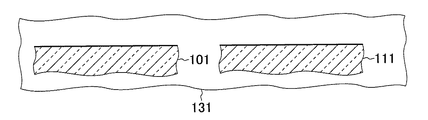
はじめに、本発明の実施の形態1について説明する。図1A〜図1Cは、本発明の実施の形態1における接合方法を説明するための工程図である。図1A〜図1Cでは、接合対象となる水晶基板101および水晶基板111の一部断面を示している。
[Embodiment 1]
First,
まず、図1Aに示すように、水晶基板(第1基板)101および水晶基板(第2基板)111を用意する。水晶基板101の接合面および水晶基板111の接合面は、よく知られた研磨などにより、表面粗さが1nm未満の状態としておく。次に、水晶基板101および水晶基板111を、真空成膜法(例えばスパッタ法)による成膜装置(スパッタ装置)の処理室131内に搬入する。
First, as shown in FIG. 1A, a quartz substrate (first substrate) 101 and a quartz substrate (second substrate) 111 are prepared. The bonding surface of the
次に、図1Bに示すように、水晶基板101の接合面および水晶基板111の接合面に、真空成膜法による物質層102の形成を開始する。例えば、よく知られたスパッタ法により、水晶基板101の接合面に対する物質層102の形成、および水晶基板111の接合面に対する物質層102の形成を開始する。
Next, as shown in FIG. 1B, the formation of the
例えば、成膜装置としてマグネトロンスパッタ装置を用い、まず、水晶基板101および水晶基板111を搬入した処理室131の内部を、圧力10-6Pa程度にまで排気する。次に、処理室131内にスパッタガスとしてアルゴンガスを導入し、また、プラズマパワーを入力し、処理室内にプラズマを生成させ、スパッタ成膜を開始する。ここで、スパッタガスには、アルゴンなどの不活性ガスを用いる。また、ターゲットには、物質層102を構成する材料を用いる。例えば、ターゲットは、Crである。この場合、Crの層が物質層102として形成される。
For example, a magnetron sputtering apparatus is used as the film forming apparatus, and first, the inside of the
以上のように、処理室131内で物質層102の成膜を開始した後、0.2nm以上1nm未満の層厚の物質層102が各々形成された水晶基板101の接合面および水晶基板111の接合面とを、物質層102を介して着接する。なお、この着接においては、圧力を加える必要はない。例えば、2つの基板を保持し、また当接させる治具(不図示)を処理室131の内部に配置し、この治具を用いて着接させればよい(特許文献1参照)。基板の自重程度で接合ができる。
As described above, after starting the formation of the
上述したことにより、図1Cに示すように、物質層102を介し、水晶基板101と水晶基板111とを各々の接合面で接合する。水晶基板101と水晶基板111との貼り合わせは、0.2nm以上1nm未満の層厚の物質層102が形成されたら、上述したスパッタ状態を停止し、この後(直後)で行ってもよく、スパッタ状態を継続している中で行ってもよい。物質層102の層厚が、1nmになる前に、2つの基板の着接を行うことが重要である。
As described above, as shown in FIG. 1C, the
なお、物質層102は、Crの他、例えばTi,Ta,Cu,およびAlなどの金属より構成することもできる。以下、物質層102に、Ti,Cr,およびTaを用いた場合の、物質層102の層厚と接合強度(引張り強度)との関係について説明する。
In addition, the
図2は、物質層102の層厚と接合強度(引張り強度)との関係を示す特性図である。この結果は、成膜してから30秒後に貼り合わせ(着接)を行っている。図中白四角は、物質層102をTiより構成した結果を示し、白丸は、物質層102をCrから構成した場合を示し、白三角は、物質層をTaらか構成した場合を示している。なお、ここでいう「層厚」は、一方の基板に形成された物質層102の厚さを表す。図2から明らかなように、材料にかかわらず、物質層102の層厚が1nm未満の引張り強度(接合力)は約25MPa以上であり、物質層102の層厚を1nm未満とすることで、強い接合強度が得られる。なお、物質層102の層厚を、1nm未満とするので、基板の表面粗さを1nm未満としておくことが重要となる。
FIG. 2 is a characteristic diagram showing the relationship between the thickness of the
ここで、物質層の層厚を1nm未満とすることでより強い接合強度が得られることについて説明する。上述した本実施の形態における接合方法は、まず、高い真空状態のほぼ酸素がなく清浄な環境下で、基板の接合面に極薄い物質層を形成し、この物質層を構成する物質の拡散現象を利用して2つの基板を接合しているものと考えることができる。この接合方法では、物質層が一様な膜となる前の不完全な層の状態の方が、活性が高く拡散速度も高いため、より高い接合強度が得られるものと考えられる。ここで、接合を行う処理室の内部は、10-6Pa以下の圧力(真空度)としておけば、自然酸化膜の形成が抑制されて十分な清浄環境となり、上述した接合が行えることが実験の結果判明している。例えば、スパッタを開始する前の初期段階で、処理室内を10-6Pa以下の圧力としておけばよい。また、スパッタを停止してからスパッタガスの供給を停止してより高い真空度としてから、着接を行って接合してもよい。なお、物質層としてAu,Pt,Agなどの貴金属や動などの酸化しにくい金属を用いる場合、接合を行う処理室の内部圧力が、10-4Pa程度であっても上述した接合が行える。 Here, it will be described that stronger bonding strength can be obtained by setting the thickness of the material layer to less than 1 nm. In the bonding method in the present embodiment described above, first, a very thin material layer is formed on the bonding surface of the substrate in a clean environment without oxygen in a high vacuum state, and the diffusion phenomenon of the material constituting this material layer It can be considered that two substrates are bonded using the above. In this bonding method, the state of the incomplete layer before the material layer becomes a uniform film is more active and has a higher diffusion rate. Therefore, it is considered that higher bonding strength can be obtained. Here, if the inside of the processing chamber in which the bonding is performed is set to a pressure (vacuum degree) of 10 −6 Pa or less, the formation of the natural oxide film is suppressed and the environment becomes sufficiently clean, and the above-described bonding can be performed. The results are known. For example, the pressure in the processing chamber may be set to 10 −6 Pa or less in the initial stage before starting sputtering. Alternatively, after sputter is stopped, the supply of the sputtering gas is stopped to obtain a higher degree of vacuum, and then attachment may be performed for bonding. In the case where a noble metal such as Au, Pt, or Ag or a metal that is difficult to oxidize such as dynamic is used as the material layer, the above-described bonding can be performed even if the internal pressure of the processing chamber for bonding is about 10 −4 Pa.
この接合方法によると、基板の接合面に活性な面を露出させるためのエッチングなどを行わないので、水晶などのエッチング異方性のある基板であっても、安定した接合が行える。また、この接合方法では、加熱処理などを必要としないので、耐熱性の低い基板であっても容易に適用可能であり、また、加熱によるプロセスコストの削減も可能となる。 According to this bonding method, since etching for exposing an active surface to the bonding surface of the substrate is not performed, stable bonding can be performed even with a substrate having etching anisotropy such as quartz. In addition, since this bonding method does not require heat treatment or the like, even a substrate with low heat resistance can be easily applied, and the process cost by heating can be reduced.
また、物質層102を1nm未満(0.2nm以上)の層厚とすることで、まず、水晶光学素子の場合、水晶基板の光透過特性を損なうことがない。このように薄い層であれば、可視光の範囲であればほとんど吸収がなく、様々の光学素子として問題なく用いることができる。また、水晶圧電素子の場合、様々な配線が形成されている水晶基板が貼り合わせの対象となる。このような場合であっても、物質層102が金属材料から構成されていても、物質層102が1nm未満と薄く高い抵抗が得られているため、物質層102の絶縁性についたは問題とならない。よく知られているように、厚さが2nm以下の金属層であれば、高い絶縁性が得られる。
In addition, by setting the
以上に説明したように、本実施の形態によれば、物質層の層厚を0.2nm以上1nm未満としたので、物質層を介した2つの基板をより十分な接合強度で接合できるようになる。また、接合した2つの基板の間に介在する物質層が非常に薄いので、光学素子として用いる場合においても光学特性の劣化を招くことがない。また、物質層が非常に薄く、物質層においては、高い絶縁状態が得られているので、圧電素子に適用しても、短絡などを招くことがない。また、高温に加熱することがなく、応力の発生などによる破損などが抑制できるようになる。 As described above, according to the present embodiment, since the thickness of the material layer is set to 0.2 nm or more and less than 1 nm, the two substrates through the material layer can be bonded with more sufficient bonding strength. Become. In addition, since a material layer interposed between two bonded substrates is very thin, optical characteristics are not deteriorated even when used as an optical element. In addition, since the material layer is very thin and a high insulating state is obtained in the material layer, a short circuit or the like is not caused even when applied to a piezoelectric element. Further, it is not heated to a high temperature, and breakage due to generation of stress can be suppressed.
[実施の形態2]
次に、本発明の実施の形態2について説明する。実施の形態2では、圧電素子(水晶素子)を例に説明し、特に、圧電素子の封止を例に説明する。
[Embodiment 2]
Next, a second embodiment of the present invention will be described. In the second embodiment, a piezoelectric element (quartz element) is described as an example, and in particular, sealing of a piezoelectric element is described as an example.
まず、図3Aに示すように、圧電素子301を水晶からなる支持基板302の上に搭載(実装)する。圧電素子301は、よく知られているように、例えば水晶などの圧電基板303に所定の電極304および配線305が形成されて構成された水晶振動子である。また、支持基板302は、配線305に接続して圧電素子301の端部を支持固定する導電性を有する支持部306,支持部306を介して配線305に接続する配線307,ビア配線308,および外部端子309が形成されている。圧電素子301は、支持部306により支持基板302に実装される。
First, as shown in FIG. 3A, the piezoelectric element 301 is mounted (mounted) on a
次に、図3Bに示すように、水晶からなる封止基板311を用意する。封止基板301には、圧電素子301の部分に対応して凹部312が形成されている。
Next, as shown in FIG. 3B, a sealing
次に、支持基板301および封止基板311を、真空成膜法(例えばスパッタ法)による成膜装置(スパッタ装置)の処理室内に搬入する。なお、成膜装置および処理室などは、図示していない。引き続いて、図3Cおよび図3Dに示すように、支持基板302の圧電素子301が搭載されている面(膜形成面)、および、封止基板311の凹部312が形成されている面(膜形成面)に、真空成膜法による物質層321の形成を開始する。例えば、よく知られたスパッタ法により、支持基板301の膜形成面に対する物質層321の形成、および封止基板311の膜形成面に対する物質層321の形成を開始する。例えば、成膜装置としてマグネトロンスパッタ装置を用い、アルミニウム(Al)をターゲットとしてAlからなる物質層321の形成を開始すればよい。
Next, the support substrate 301 and the sealing
以上のように、処理室内で物質層321の成膜を開始した後、0.2nm以上1nm未満の層厚の物質層321が各々形成された支持基板301の接合面および封止基板311の接合面とを、物質層321を介して着接する。なお、この着接においては、圧力を加える必要はない。
As described above, after the deposition of the
上述したことにより、図3Eに示すように、物質層321を介し、支持基板301と封止基板311とを各々の接合面で接合すれば、圧電素子301が支持基板301と封止基板311とによる容器の中に封止された水晶素子が得られる。圧電素子301は、物質層321を介して接合された支持基板301および封止基板311により、凹部312の内部に封止される。ここで、支持基板301と封止基板311との貼り合わせは、0.2nm以上1nm未満の層厚の物質層321が形成されたら、上述したスパッタ状態を停止し、この後(直後)で行ってもよく、スパッタ状態を継続している中で行ってもよい。物質層321の層厚が1nmになる前に、2つの基板の着接を行うことが重要である。
As described above, as illustrated in FIG. 3E, when the support substrate 301 and the sealing
ここで、物質層321は、例えば、支持基板301の上の全域に形成される。このため、例えば、支持基板301の上に形成されている複数の配線307に渡って物質層321が形成されることになる。物質層321をAlなどの金属より構成した場合、金属層により各配線307の間が接続されることになる。しかしながら、物質層321は、層厚1nm未満と薄くしているので、高い絶縁性を有した状態となっており、各配線307の間で電気的な短絡を招くことがない。図4に示すように、例えば、Au,Tiなどの金属であれば、層厚1nm未満では、高い膜抵抗値となり、十分な絶縁性が確保できる。
Here, the
[実施の形態3]
次に、本発明の実施の形態3について説明する。実施の形態3では、光学素子を例に説明し、特に、接合により作製される光学素子を例に説明する。
[Embodiment 3]
Next, a third embodiment of the present invention will be described. In
本実施の形態における接合方法で作製された光学素子(水晶素子)は、例えば、図5に示すように、水晶基板501と水晶基板502とが、物質層503を介して接合されている。水晶基板501は平均表面粗さRa<1nm、水晶基板502は平均表面粗さRaが0.3nmとされている。
In the optical element (quartz element) manufactured by the bonding method in the present embodiment, for example, as shown in FIG. 5, a
例えば、水晶基板501および水晶基板502を、真空成膜法(例えばスパッタ法)による成膜装置(スパッタ装置)の処理室内に搬入する。引き続いて、支持基板302の接合面、および、水晶基板502の接合面に、真空成膜法による物質層503の形成を開始する。例えば、よく知られたスパッタ法により、水晶基板501の接合面に対する物質層503の形成、および水晶基板502の接合面に対する物質層503の形成を開始する。例えば、成膜装置としてマグネトロンスパッタ装置を用い、アルミニウム(Al)をターゲットとしてAlからなる物質層503の形成を開始すればよい。
For example, the
以上のように、処理室内で物質層503の成膜を開始した後、0.2nm以上1nm未満の層厚の物質層503が各々形成された水晶基板501の接合面および水晶基板502の接合面とを、物質層503を介して着接する。例えば、各々の接合面に、0.4nmの物質層503が形成されたら、接着を行う。なお、この着接においては、圧力を加える必要はない。
As described above, after the deposition of the
上述したことにより、物質層503を介し、水晶基板501と水晶基板502とが各々の接合面で接合される。水晶基板501と水晶基板502との貼り合わせは、0.2nm以上1nm未満の層厚の物質層503が形成されたら、上述したスパッタ状態を停止し、この後(直後)で行ってもよく、スパッタ状態を継続している中で行ってもよい。水晶板501の接合面に形成される物質層503および水晶板502の接合面に形成される物質層503の各々の層厚が1nmになる前に、2つの基板の着接を行うことが重要である。
As described above, the
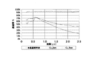
ここで、上述した本実施の形態における光学素子の特性評価結果について説明する。本実施の形態における光学素子と、従来の有機系接着剤で接着された光学素子について、透過波面収差の測定を行い、P−V(Peak-Valley)値を比較した。透過波面収差の測定は、フィゾー干渉計により行い、測定波長は632.8nmとし、測定領域は、物質層503により接続している領域の中央部の直径13mmの円形領域とする。測定の結果、従来の有機系接着剤で接着された光学素子のP−V値が1wave以上であるのに対し、本実施の形態における光学素子のP−V値は、0.1wave以下と非常に小さく良好な特性が確認できた。
Here, the characteristic evaluation result of the optical element in this Embodiment mentioned above is demonstrated. The transmitted wavefront aberration was measured for the optical element in the present embodiment and the optical element bonded with a conventional organic adhesive, and the PV (Peak-Valley) values were compared. The transmitted wavefront aberration is measured by a Fizeau interferometer, the measurement wavelength is 632.8 nm, and the measurement region is a circular region having a diameter of 13 mm at the center of the region connected by the
有機系接着剤の厚さは10μm以上となり、接着固定時に接着層の厚さに不均一が発生し、また、接着時の部分的な応力による屈折率の不均一さが、有機系接着剤で接着された光学素子における透過波面の劣化につながっているものと考えられる。これに対し、本実施の形態における接合方法で接合された光学素子は、接合部となる物質層503の合計の層厚が、2nm未満と非常に薄くかつ均一のため、非常に良好な透過波面が得られるものと考えられる。
The thickness of the organic adhesive is 10 μm or more, and non-uniformity occurs in the thickness of the adhesive layer at the time of bonding and fixing, and non-uniform refractive index due to partial stress at the time of bonding is caused by the organic adhesive. It is considered that the transmission wavefront in the bonded optical element is deteriorated. On the other hand, the optical element bonded by the bonding method according to the present embodiment has a very good transmitted wavefront because the total layer thickness of the
なお、物質層503は、Alに限らず、Au,Ti,Ta,Cu,Crなどの金属でもよく、また、Siなどの半導体材料でもよい。
Note that the
ところで、光学素子においては、所望の透過率(高い透明性)が得られていることが重要となるが、上述したように、一方の接合面に形成される物質層の層厚が1nm未満であれば、透明性に影響を与えることがない。 By the way, in an optical element, it is important that a desired transmittance (high transparency) is obtained. As described above, the thickness of the material layer formed on one bonding surface is less than 1 nm. If there is, it does not affect transparency.
例えば、図6,図7に示すように、CrおよびSiの場合、一方の接合面に形成される物質層の層厚が0.2nmおよび0.4nmのいずれの場合も、ほぼ75%以上の透過率が得られている。また、図8,図9に示すように、Cu,Ti,Taの場合、一方の接合面に形成される物質層の層厚が0.2nmであれば、ほぼ75%以上の透過率が得られている。なお、Taの場合、層厚が0.4nmの場合、0.2μm近辺の波長域の透過率が70%程度となる。 For example, as shown in FIGS. 6 and 7, in the case of Cr and Si, when the thickness of the material layer formed on one joint surface is 0.2 nm or 0.4 nm, it is approximately 75% or more. The transmittance is obtained. Further, as shown in FIGS. 8 and 9, in the case of Cu, Ti, and Ta, if the thickness of the material layer formed on one bonding surface is 0.2 nm, a transmittance of approximately 75% or more is obtained. It has been. In the case of Ta, when the layer thickness is 0.4 nm, the transmittance in the wavelength region near 0.2 μm is about 70%.
一方、一方の接合面に形成される物質層の層厚が1nmを超えて厚くなると、図10に示すように、透過率が低下するようになる。特に、Cuの場合、一方の接合面に形成される物質層の層厚が5nmでは、2.5μm近辺の波長域の透過率が20%程度となる。また、図11に示すように、本実施の形態における光学素子によれば、貼り合わせに有機系接着剤を用いた場合に比較して、紫外域の光学的な損失率の低下が大幅に抑制されるようになる。損失率は、物質層や接着剤を用いずに、2つの水晶基板のみを透過させた光量Pと、1つの水晶基板が物質層もしくは接着剤により接合された状態で透過させた光量P’を用い、損失率(%)={(P−P’)/P}×100により求めている。なお、図11の結果は、物質層にCuおよびTiを用いた場合の結果を示している。 On the other hand, when the thickness of the material layer formed on one bonding surface exceeds 1 nm, the transmittance decreases as shown in FIG. In particular, in the case of Cu, when the thickness of the material layer formed on one bonding surface is 5 nm, the transmittance in the wavelength region near 2.5 μm is about 20%. In addition, as shown in FIG. 11, according to the optical element in the present embodiment, a decrease in the optical loss rate in the ultraviolet region is significantly suppressed as compared with the case where an organic adhesive is used for bonding. Will come to be. The loss rate is determined by the amount of light P transmitted through only two crystal substrates without using a material layer or an adhesive, and the amount of light P ′ transmitted through one crystal substrate bonded with a material layer or an adhesive. The loss rate (%) = {(PP ′) / P} × 100. In addition, the result of FIG. 11 has shown the result at the time of using Cu and Ti for a material layer.
次に、より長波長領域(波長2.5〜5μm)における透過率の測定結果について説明する。まず、貼り合わせ(接合)に有機系接着剤を用いた場合、図12に示すように、接着剤に含まれている成分に対応する吸収が確認される。 Next, the measurement result of the transmittance in a longer wavelength region (wavelength 2.5 to 5 μm) will be described. First, when an organic adhesive is used for bonding (bonding), as shown in FIG. 12, the absorption corresponding to the component contained in the adhesive is confirmed.
上述の結果に対し、本実施の形態における物質層を用いた貼り合わせの場合、図13に示すように、有機系接着剤を用いた場合に比較してより高い透過率が得られている。 In contrast to the above results, in the case of bonding using the material layer in the present embodiment, a higher transmittance is obtained as compared with the case where an organic adhesive is used, as shown in FIG.
なお、本発明は以上に説明した実施の形態に限定されるものではなく、本発明の技術的思想内で、当分野において通常の知識を有する者により、多くの変形が実施可能であることは明白である。例えば、スパッタ法に限らず、公知のイオンプレーティング法で物質層を形成してもよい。これらは、プラズマの発生下で成膜が行われる真空成膜法である。また、真空蒸着法など、他の真空成膜法であってもよい。 It should be noted that the present invention is not limited to the embodiment described above, and that many modifications can be implemented by those having ordinary knowledge in the art within the technical idea of the present invention. It is obvious. For example, the material layer may be formed not only by the sputtering method but also by a known ion plating method. These are vacuum film formation methods in which film formation is performed under generation of plasma. Moreover, other vacuum film-forming methods, such as a vacuum evaporation method, may be used.
また、接合対象の基板に反りがある場合、接合面同士が接触するように、2つの基板の間に荷重を加えてもよい。また、上述では、Ti,Cr,およびTaを用いた実験結果について示したが、物質層は、これらの材料に限るものではなく、Au,Cu,Alなどの他の金属材料でもよいことはいうまでもない。また、物質層は、Si,Geなどの半導体材料から構成されていてもよい。 In addition, when the substrates to be bonded are warped, a load may be applied between the two substrates so that the bonding surfaces come into contact with each other. In the above description, experimental results using Ti, Cr, and Ta have been described. However, the material layer is not limited to these materials, and other metal materials such as Au, Cu, and Al may be used. Not too long. The substance layer may be made of a semiconductor material such as Si or Ge.
また、上述では、水晶基板に水晶基板を貼り合わせる場合を例に説明したが、これに限るものではなく、一方の基板が、ガラス,シリコンなどの他の材料から構成されている基板であっても同様に接合可能である。また、上述では、圧電素子として、水晶振動子を例にしたが、これに限るものではなく、よく知られた表面弾性波 (Surface Acoustic Wave:SAW) 素子であっても同様である。 In the above description, the case where the quartz substrate is bonded to the quartz substrate has been described as an example. However, the present invention is not limited to this, and one substrate is a substrate made of another material such as glass or silicon. Can be joined in the same manner. In the above description, the quartz resonator is taken as an example of the piezoelectric element. However, the present invention is not limited to this, and the same applies to a well-known surface acoustic wave (SAW) element.
101…水晶基板、102…物質層、111…水晶基板、131…処理室。
DESCRIPTION OF
Claims (8)
前記処理室内で、0.2nm以上1nm未満の層厚の前記物質層が各々形成された前記第1基板の接合面および前記第2基板の接合面を、前記物質層を介して着接して前記第1基板と前記第2基板とを各々の接合面で接合する第2工程と
を少なくとも備え、
前記第1基板の接合面および前記第2基板の接合面は、平均表面粗さが1nm未満とされていることを特徴とする接合方法。 A first step of starting the formation of the material layer by the vacuum film formation method on the bonding surface of the first substrate and the bonding surface of the second substrate made of quartz in the processing chamber of the film formation apparatus by the vacuum film formation method;
In the processing chamber, the bonding surface of the first substrate and the bonding surface of the second substrate on which the material layers each having a layer thickness of 0.2 nm or more and less than 1 nm are formed are attached and bonded via the material layer. A second step of bonding the first substrate and the second substrate at each bonding surface; and
An average surface roughness of the bonding surface of the first substrate and the bonding surface of the second substrate is less than 1 nm.
前記第2工程は、前記真空成膜法による前記物質層の形成を停止した後で行うことを特徴とする接合方法。 The joining method according to claim 1,
The bonding method, wherein the second step is performed after the formation of the material layer by the vacuum film-forming method is stopped.
前記第1基板は、水晶から構成されていることを特徴とする接合方法。 The joining method according to claim 1 or 2,
The bonding method according to claim 1, wherein the first substrate is made of quartz.
前記真空成膜法は、スパッタ法およびイオンプレーティング法より選択された方法であることを特徴とする接合方法。 In the joining method according to any one of claims 1 to 3,
The vacuum deposition method is a method selected from a sputtering method and an ion plating method.
前記物質層は、金属または半導体材料より構成されていることを特徴とする接合方法。 In the joining method according to any one of claims 1 to 4,
The bonding method according to claim 1, wherein the material layer is made of a metal or a semiconductor material.
前記水晶素子は、水晶からなる前記第1基板および前記第2基板が前記物質層を介して接合された光学素子であることを特徴とする水晶素子。 The crystal element according to claim 6, wherein
The quartz crystal element is an optical element in which the first substrate and the second substrate made of quartz are bonded via the material layer.
前記水晶素子は、前記第1基板の上に搭載された圧電素子と、この圧電素子に対応して形成された凹部を備える前記第2基板とを備え、
前記圧電素子は、前記物質層を介して接合された前記第1基板および前記第2基板により前記凹部の内部に封止されている
ことを特徴とする水晶素子。 The crystal element according to claim 6, wherein
The crystal element includes a piezoelectric element mounted on the first substrate, and the second substrate including a recess formed corresponding to the piezoelectric element,
The piezoelectric element is sealed inside the recess by the first substrate and the second substrate bonded through the material layer.
Priority Applications (1)
| Application Number | Priority Date | Filing Date | Title |
|---|---|---|---|
| JP2010054208A JP2011187867A (en) | 2010-03-11 | 2010-03-11 | Bonding method and crystal element |
Applications Claiming Priority (1)
| Application Number | Priority Date | Filing Date | Title |
|---|---|---|---|
| JP2010054208A JP2011187867A (en) | 2010-03-11 | 2010-03-11 | Bonding method and crystal element |
Publications (2)
| Publication Number | Publication Date |
|---|---|
| JP2011187867A true JP2011187867A (en) | 2011-09-22 |
| JP2011187867A5 JP2011187867A5 (en) | 2013-03-14 |
Family
ID=44793753
Family Applications (1)
| Application Number | Title | Priority Date | Filing Date |
|---|---|---|---|
| JP2010054208A Pending JP2011187867A (en) | 2010-03-11 | 2010-03-11 | Bonding method and crystal element |
Country Status (1)
| Country | Link |
|---|---|
| JP (1) | JP2011187867A (en) |
Cited By (4)
| Publication number | Priority date | Publication date | Assignee | Title |
|---|---|---|---|---|
| JP2014186887A (en) * | 2013-03-25 | 2014-10-02 | Kyocera Crystal Device Corp | Window member for optical equipment |
| JP2016050863A (en) * | 2014-09-01 | 2016-04-11 | 京セラクリスタルデバイス株式会社 | Optical cell and manufacturing method thereof |
| US11539346B2 (en) | 2019-01-31 | 2022-12-27 | Seiko Epson Corporation | Resonator device, resonator module, electronic apparatus, and vehicle |
| US11575361B2 (en) | 2019-01-31 | 2023-02-07 | Seiko Epson Corporation | Resonator device, resonator module, electronic apparatus, and vehicle |
Citations (3)
| Publication number | Priority date | Publication date | Assignee | Title |
|---|---|---|---|---|
| JP2008207221A (en) * | 2007-02-27 | 2008-09-11 | Takehito Shimazu | Room temperature joining method |
| JP2009206759A (en) * | 2008-02-27 | 2009-09-10 | Seiko Instruments Inc | Piezoelectric vibration chip, piezoelectric vibrator, oscillator, electronic apparatus, radio wave clock, and method of manufacturing piezoelectric vibration chip |
| JP2010046696A (en) * | 2008-08-22 | 2010-03-04 | Musashino Eng:Kk | Nuclear diffusion joining method and structure joined thereby |
-
2010
- 2010-03-11 JP JP2010054208A patent/JP2011187867A/en active Pending
Patent Citations (3)
| Publication number | Priority date | Publication date | Assignee | Title |
|---|---|---|---|---|
| JP2008207221A (en) * | 2007-02-27 | 2008-09-11 | Takehito Shimazu | Room temperature joining method |
| JP2009206759A (en) * | 2008-02-27 | 2009-09-10 | Seiko Instruments Inc | Piezoelectric vibration chip, piezoelectric vibrator, oscillator, electronic apparatus, radio wave clock, and method of manufacturing piezoelectric vibration chip |
| JP2010046696A (en) * | 2008-08-22 | 2010-03-04 | Musashino Eng:Kk | Nuclear diffusion joining method and structure joined thereby |
Cited By (4)
| Publication number | Priority date | Publication date | Assignee | Title |
|---|---|---|---|---|
| JP2014186887A (en) * | 2013-03-25 | 2014-10-02 | Kyocera Crystal Device Corp | Window member for optical equipment |
| JP2016050863A (en) * | 2014-09-01 | 2016-04-11 | 京セラクリスタルデバイス株式会社 | Optical cell and manufacturing method thereof |
| US11539346B2 (en) | 2019-01-31 | 2022-12-27 | Seiko Epson Corporation | Resonator device, resonator module, electronic apparatus, and vehicle |
| US11575361B2 (en) | 2019-01-31 | 2023-02-07 | Seiko Epson Corporation | Resonator device, resonator module, electronic apparatus, and vehicle |
Similar Documents
| Publication | Publication Date | Title |
|---|---|---|
| TWI664754B (en) | Joint body and elastic wave device | |
| US10964882B2 (en) | Bonding method | |
| JP4993204B2 (en) | Piezoelectric vibrator and manufacturing method thereof | |
| CN110463038A (en) | Conjugant and elastic wave device | |
| US4247034A (en) | Method of indirectly connecting two parts | |
| JP4348454B2 (en) | Device and device manufacturing method | |
| US8585220B2 (en) | Optical element and method of producing same | |
| JP2011187867A (en) | Bonding method and crystal element | |
| US20210111698A1 (en) | Bonded body and elastic wave element | |
| EP2952972A1 (en) | Method for manufacturing a composite compensator spiral | |
| US11139427B2 (en) | Bonded body and elastic wave element | |
| WO2019138875A1 (en) | Functional element, method for manufacturing functional element, and electronic device | |
| CN109964405A (en) | Conjugant | |
| JP2018093329A (en) | Elastic wave element | |
| JP2013238738A (en) | Optical device and method for manufacturing the same | |
| JP2014192653A (en) | Piezoelectric device and process of manufacturing the same | |
| US20130327093A1 (en) | Method of producing lightweight structural elements | |
| WO2020148911A1 (en) | Deformable mirror and method for manufacturing same | |
| WO2021225101A1 (en) | Piezoelectric composite substrate and method for manufacturing same | |
| EP0153232A2 (en) | Process for hermetically sealing metallic objects onto a glass-ceramic body | |
| Cheung | Die-level glass frit vacuum packaging for a micro-fuel processor system | |
| JP5950962B2 (en) | Optical element manufacturing method | |
| EP4131777A1 (en) | Bonded body and method for producing same | |
| TWI791590B (en) | Method for joining quartz pieces and quartz electrodes and other devices of joined quartz | |
| WO2022172902A1 (en) | Chemical bonding method, package-type electronic component, and hybrid bonding method for electronic device |
Legal Events
| Date | Code | Title | Description |
|---|---|---|---|
| A521 | Request for written amendment filed |
Free format text: JAPANESE INTERMEDIATE CODE: A523 Effective date: 20130130 |
|
| A621 | Written request for application examination |
Free format text: JAPANESE INTERMEDIATE CODE: A621 Effective date: 20130130 |
|
| A131 | Notification of reasons for refusal |
Free format text: JAPANESE INTERMEDIATE CODE: A131 Effective date: 20140212 |
|
| A02 | Decision of refusal |
Free format text: JAPANESE INTERMEDIATE CODE: A02 Effective date: 20140624 |