JP2011181599A - Apparatus and method for plasma film-forming - Google Patents
Apparatus and method for plasma film-forming Download PDFInfo
- Publication number
- JP2011181599A JP2011181599A JP2010042554A JP2010042554A JP2011181599A JP 2011181599 A JP2011181599 A JP 2011181599A JP 2010042554 A JP2010042554 A JP 2010042554A JP 2010042554 A JP2010042554 A JP 2010042554A JP 2011181599 A JP2011181599 A JP 2011181599A
- Authority
- JP
- Japan
- Prior art keywords
- substrate
- film
- plasma
- borazine
- electrode
- Prior art date
- Legal status (The legal status is an assumption and is not a legal conclusion. Google has not performed a legal analysis and makes no representation as to the accuracy of the status listed.)
- Pending
Links
Images


Classifications
-
- C—CHEMISTRY; METALLURGY
- C23—COATING METALLIC MATERIAL; COATING MATERIAL WITH METALLIC MATERIAL; CHEMICAL SURFACE TREATMENT; DIFFUSION TREATMENT OF METALLIC MATERIAL; COATING BY VACUUM EVAPORATION, BY SPUTTERING, BY ION IMPLANTATION OR BY CHEMICAL VAPOUR DEPOSITION, IN GENERAL; INHIBITING CORROSION OF METALLIC MATERIAL OR INCRUSTATION IN GENERAL
- C23C—COATING METALLIC MATERIAL; COATING MATERIAL WITH METALLIC MATERIAL; SURFACE TREATMENT OF METALLIC MATERIAL BY DIFFUSION INTO THE SURFACE, BY CHEMICAL CONVERSION OR SUBSTITUTION; COATING BY VACUUM EVAPORATION, BY SPUTTERING, BY ION IMPLANTATION OR BY CHEMICAL VAPOUR DEPOSITION, IN GENERAL
- C23C16/00—Chemical coating by decomposition of gaseous compounds, without leaving reaction products of surface material in the coating, i.e. chemical vapour deposition [CVD] processes
- C23C16/44—Chemical coating by decomposition of gaseous compounds, without leaving reaction products of surface material in the coating, i.e. chemical vapour deposition [CVD] processes characterised by the method of coating
- C23C16/50—Chemical coating by decomposition of gaseous compounds, without leaving reaction products of surface material in the coating, i.e. chemical vapour deposition [CVD] processes characterised by the method of coating using electric discharges
- C23C16/505—Chemical coating by decomposition of gaseous compounds, without leaving reaction products of surface material in the coating, i.e. chemical vapour deposition [CVD] processes characterised by the method of coating using electric discharges using radio frequency discharges
- C23C16/509—Chemical coating by decomposition of gaseous compounds, without leaving reaction products of surface material in the coating, i.e. chemical vapour deposition [CVD] processes characterised by the method of coating using electric discharges using radio frequency discharges using internal electrodes
-
- H—ELECTRICITY
- H01—ELECTRIC ELEMENTS
- H01J—ELECTRIC DISCHARGE TUBES OR DISCHARGE LAMPS
- H01J37/00—Discharge tubes with provision for introducing objects or material to be exposed to the discharge, e.g. for the purpose of examination or processing thereof
- H01J37/32—Gas-filled discharge tubes
- H01J37/32009—Arrangements for generation of plasma specially adapted for examination or treatment of objects, e.g. plasma sources
- H01J37/32082—Radio frequency generated discharge
- H01J37/321—Radio frequency generated discharge the radio frequency energy being inductively coupled to the plasma
-
- H—ELECTRICITY
- H01—ELECTRIC ELEMENTS
- H01J—ELECTRIC DISCHARGE TUBES OR DISCHARGE LAMPS
- H01J37/00—Discharge tubes with provision for introducing objects or material to be exposed to the discharge, e.g. for the purpose of examination or processing thereof
- H01J37/32—Gas-filled discharge tubes
- H01J37/32009—Arrangements for generation of plasma specially adapted for examination or treatment of objects, e.g. plasma sources
- H01J37/32082—Radio frequency generated discharge
- H01J37/32137—Radio frequency generated discharge controlling of the discharge by modulation of energy
- H01J37/32155—Frequency modulation
- H01J37/32165—Plural frequencies
-
- H—ELECTRICITY
- H01—ELECTRIC ELEMENTS
- H01J—ELECTRIC DISCHARGE TUBES OR DISCHARGE LAMPS
- H01J37/00—Discharge tubes with provision for introducing objects or material to be exposed to the discharge, e.g. for the purpose of examination or processing thereof
- H01J37/32—Gas-filled discharge tubes
- H01J37/32431—Constructional details of the reactor
- H01J37/32532—Electrodes
- H01J37/32541—Shape
Abstract
Description
本発明は、原料ガスをプラズマ状態にして、基板上に成膜を行うプラズマ成膜装置及び方法に関する。 The present invention relates to a plasma film forming apparatus and method for forming a film on a substrate by making a source gas into a plasma state.
プラズマ成膜装置、例えば、プラズマCVD(Chemical Vapor Deposition)装置は、原料ガスをプラズマ状態にし、プラズマ状態の原料ガス同士を反応させて、基板上に成膜を行っている。成膜の際には、成膜した膜質を向上させる目的等の理由から、基板にバイアスを印加することが多い。 A plasma film forming apparatus, for example, a plasma CVD (Chemical Vapor Deposition) apparatus forms a film on a substrate by bringing a raw material gas into a plasma state and causing the raw material gases in a plasma state to react with each other. In film formation, a bias is often applied to the substrate for the purpose of improving the quality of the formed film.
基板にバイアスを印加して成膜を行う場合、基板外周部分の膜厚が高くなってしまい、所望の膜厚均一性を得ることができない場合があった。特に、絶縁系膜、例えば、窒化珪素膜、ボラジン膜等において、基板外周部分の膜厚が高くなる傾向があった。例えば、従来のプラズマCVD装置で成膜したボラジン膜の半径方向(X軸位置)の膜厚を、バイアス(LF)の印加電圧を変えて、測定した結果を、図5に示す。図5からわかるように、LF:0W、つまり、バイアス印加が0のときには、基板外周部分(図5中の領域A参照)の膜厚が基板中心部分より若干低くなるのに対して、LF:50W、100W、180Wのときには、つまり、バイアス印加があるときには、基板外周部分(図5中の領域A参照)の膜厚が基板中心部分より高くなっており、所望の膜厚均一性を得ることができなかった。 When a film is formed by applying a bias to the substrate, the film thickness at the outer periphery of the substrate becomes high, and a desired film thickness uniformity may not be obtained. In particular, in an insulating film such as a silicon nitride film or a borazine film, the film thickness at the outer peripheral portion of the substrate tends to increase. For example, FIG. 5 shows the results of measuring the radial thickness (X-axis position) of a borazine film formed by a conventional plasma CVD apparatus while changing the bias (LF) applied voltage. As can be seen from FIG. 5, when LF: 0 W, that is, when the bias application is 0, the film thickness of the outer peripheral portion of the substrate (see region A in FIG. 5) is slightly lower than the central portion of the substrate, whereas LF: In the case of 50 W, 100 W, and 180 W, that is, when a bias is applied, the thickness of the substrate outer peripheral portion (see region A in FIG. 5) is higher than the central portion of the substrate, and desired film thickness uniformity can be obtained. I could not.
本発明は上記課題に鑑みなされたもので、膜厚の均一性を向上させることができるプラズマ成膜装置及び方法を提供することを目的とする。 The present invention has been made in view of the above problems, and an object thereof is to provide a plasma film forming apparatus and method capable of improving the uniformity of film thickness.
上記課題を解決する第1の発明に係るプラズマ成膜装置は、
原料ガスをプラズマ状態にし、プラズマ状態の前記原料ガス同士を反応させて、基板上に成膜を行う際、前記基板にバイアスを印加するプラズマ成膜装置において、
前記基板にバイアスを印加する電極の大きさを、前記基板より大きくしたことを特徴とする。
A plasma film forming apparatus according to a first invention for solving the above-mentioned problems is as follows.
In a plasma film forming apparatus for applying a bias to the substrate when forming a film on the substrate by causing the source gas to be in a plasma state and reacting the source gases in a plasma state to each other,
The size of the electrode for applying a bias to the substrate is larger than that of the substrate.
上記課題を解決する第2の発明に係るプラズマ成膜装置は、
上記第1の発明に記載のプラズマ成膜装置において、
前記基板の半径をR1、前記電極の大きさをR2とするとき、
(R2−R1)を少なくとも1mm以上とすることを特徴とする。
A plasma film forming apparatus according to a second invention for solving the above-mentioned problems is as follows.
In the plasma film forming apparatus described in the first invention,
When the radius of the substrate is R1, and the size of the electrode is R2,
(R2-R1) is at least 1 mm or more.
上記課題を解決する第3の発明に係るプラズマ成膜方法は、
原料ガスをプラズマ状態にし、プラズマ状態の前記原料ガス同士を反応させて、基板上に成膜を行う際、前記基板にバイアスを印加するプラズマ成膜方法において、
前記基板の大きさより大きい電極を用いて、前記基板にバイアスを印加することを特徴とする。
A plasma film forming method according to a third aspect of the present invention for solving the above problem is as follows:
In the plasma film forming method of applying a bias to the substrate when forming a film on the substrate by causing the source gas to be in a plasma state and reacting the source gases in the plasma state to each other,
A bias is applied to the substrate using an electrode larger than the size of the substrate.
本発明によれば、基板にバイアスを印加する電極の大きさを基板の大きさより大きくしたので、基板外周部分の膜厚の増加を抑えることができ、膜厚の均一性を向上させることができる。 According to the present invention, since the size of the electrode for applying a bias to the substrate is made larger than the size of the substrate, it is possible to suppress an increase in the thickness of the outer peripheral portion of the substrate and improve the uniformity of the thickness. .
以下、本発明に係るプラズマ処理装置及び方法の実施形態について、図1〜図4を用いて説明する。 Hereinafter, embodiments of the plasma processing apparatus and method according to the present invention will be described with reference to FIGS.
(実施例1)
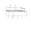
図1は、本発明に係るプラズマ処理装置の実施形態の一例を示す透視側面図であり、図2は、図1に示したプラズマ処理装置におけるバイアス印加用電極を示す概略構成図である。
Example 1
FIG. 1 is a perspective side view showing an example of an embodiment of a plasma processing apparatus according to the present invention, and FIG. 2 is a schematic configuration diagram showing a bias application electrode in the plasma processing apparatus shown in FIG.
最初に、本実施例のプラズマ処理装置について、図1を用いて説明をする。なお、図1では、一例として、ICP(Inductively Coupled Plasma)型のプラズマCVD装置1を示しているが、プラズマ発生機構を有するものであればよい。
First, the plasma processing apparatus of the present embodiment will be described with reference to FIG. In FIG. 1, an ICP (Inductively Coupled Plasma) type
本実施例のプラズマCVD装置1は、円筒状の真空チャンバ2の内部が成膜室として構成されるものであり、真空チャンバ2の上部開口部には、セラミクス製の円板状の天井板3が、開口部を塞ぐように配設されている。
The
又、天井板3の上部(直上)には、例えば、複数の円形リングからなる高周波アンテナ4が配置されており、高周波アンテナ4には整合器5を介して高周波電源6が接続されている。この高周波電源6は、後述する低周波電源13より高い発振周波数(例えば、13.56MHz)を高周波アンテナ4に給電可能となっており、真空チャンバ2内でプラズマを生成する電磁波を、天井板3を透過して入射可能なものである。これは、所謂、ICP型のプラズマ発生機構の構成である。ICP型のプラズマ発生機構により、電子密度が高いプラズマが形成可能である。
In addition, a high-
又、真空チャンバ2の下部には支持台7と、支持台7に取り付けられた静電チャック8が備えられており、この静電チャック8の上面に、Si(シリコン)等の半導体材料からなる円板状の基板Wが静電的に吸着保持されるようになっている。静電チャック8は、例えば、窒化アルミニウム(AlN)等のセラミクス材料を用いて、円板状に形成されている。又、支持台7は、昇降装置9により、その位置が上下に昇降可能となっており、成膜時に真空チャンバ2内に発生するプラズマと基板Wとの距離を調整することができるようになっている。
Further, a support base 7 and an
又、静電チャック8には、円板状の電極11が設けられており、電極11には整合器12を介して低周波電源13が接続されている。低周波電源13は、高周波電源6より低い発振周波数(例えば、4MHz)を電極11に印加し、基板Wにバイアスを印加できるようになっている。なお、本実施例の電極11は円板状に形成されているが、例えば、基板Wにオリフラ(Orientation Flat)が有る場合には、その形状に相似するように形成すればよい。
The
又、支持台7には、基板Wの温度を制御するヒータ、冷媒流路等の温度制御装置が設けられており、温度制御装置(図示省略)により、基板Wを所望の温度(例えば、150〜700℃)に設定可能となっている。 In addition, the support 7 is provided with a temperature control device such as a heater and a refrigerant flow path for controlling the temperature of the substrate W. The temperature control device (not shown) allows the substrate W to have a desired temperature (for example, 150). ˜700 ° C.).
そして、基板Wは、真空チャンバ2の側壁に設けられたゲートドア17を開けて、静電チャック8上に搬送されるようになっており静電チャック8上に載置後、ゲートドア17を閉めて、真空チャンバ2内部で後述するプロセスが実施される。
The substrate W is transported onto the
又、真空チャンバ2の側壁部分には、天井板3より低く、支持台7より高い位置に複数のガスノズル14が設けられており、ガス制御装置15により制御することにより、ガスノズル14から真空チャンバ2内部に所望の流量のガスを供給可能である。
A plurality of
又、真空チャンバ2には、圧力制御装置(真空ポンプ、圧力制御弁、真空計等;図示省略)が設けられており、真空ポンプを用いて、底部側から真空チャンバ2内部を排気すると共に、真空計、圧力制御弁を用いて、真空チャンバ2内部を所望の圧力に調整している。
Further, the
そして、上記高周波電源6、昇降装置9、低周波電源13、ガス制御装置15、温度制御装置、圧力制御装置等は、主制御装置16により統合的に制御されており、予め設定した所望のプロセス工程、プロセス条件に従って制御されている。
The high-
ここで、本実施例のプラズマCVD装置1における電極11の構成を、図2を参照して説明する。なお、比較のため、図6に従来のバイアス印加用の電極の構成を示す。
Here, the structure of the
従来のプラズマCVD装置では、図6に示すように、静電チャック21に設けたバイアス印加用の電極22の大きさを、基板Wより若干小さくしていた。例えば、基板Wの半径をR1、電極22の半径をR2とすると、R2=R1−1.0mmとすることにより、R1>R2の関係となるようにしていた。
In the conventional plasma CVD apparatus, the size of the
これに対して、本実施例のプラズマCVD装置1では、図2に示すように、バイアス印加用の電極11の大きさを、基板Wより大きくしている。例えば、基板Wの半径をR1、電極11の半径をR2とすると、R1<R2の関係となるようにしている。
On the other hand, in the
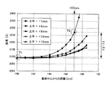
上記構成の電極11を用いた成膜結果について、図3、図4を用いて説明する。この図3は、基板外周部の膜厚の変化を、ΔR=(R2−R1)の条件を変えて測定したものであり、図4は、図3の結果に基づいて、基板外周部分の膜厚上昇率とΔRとの関係をグラフにしたものである。なお、図3、図4には、比較のため、従来の電極22を用いた成膜結果も併記している。又、プロセスの条件としては、基板Wの直径を300mm(半径R1=150mm)とし、薄膜として、LF=180Wで、ボラジン膜を成膜している。この条件は、従来の電極22を用いたときに、基板外周部の膜厚が高くなったプロセスである。
A film formation result using the
図3に示すグラフにおいて、ΔR=−1mmは、従来の電極22を用いた成膜結果を示している。これからわかるように、ΔR=−1mmの場合は、基板Wの外縁に近づくにつれて、成膜されたボラジン膜の膜厚がかなり厚くなっている。これは、基板Wにバイアスを印加する場合、基板Wの外周部分の電界強度が強くなり、その結果、基板外周部分の成膜レートが高くなったのが要因であると推測される。
In the graph shown in FIG. 3, ΔR = −1 mm indicates a film formation result using the
一方、本実施例の条件を満たすΔR=+4mmの場合には、基板Wの外縁に近づくにつれて、成膜されたボラジン膜の膜厚が厚くなっているとはいえ、その傾向はかなり改善されており、本実施例の条件を満たすΔR=+9、+14、+19mmの場合には、その傾向が更に改善されている。これは、基板Wの大きさより、電極11の大きさが大きいため、基板Wにバイアスを印加する場合、基板Wの外縁より外側にある電極11の外周部分で電界強度が強くなるため、その結果、基板外周部分の成膜レートが従来の場合より抑制されるのが要因であると推測される。
On the other hand, in the case of ΔR = + 4 mm that satisfies the conditions of this embodiment, the tendency is considerably improved although the film thickness of the formed borazine film increases as it approaches the outer edge of the substrate W. In the case of ΔR = + 9, +14, +19 mm that satisfies the conditions of the present embodiment, the tendency is further improved. This is because the size of the
図3の結果に基づいて、基板中心から140mmの位置(基板エッジから10mmの位置)の膜厚をT1とし、基板中心から147mmの位置(基板エッジから3mmの位置)の膜厚をT2とし、条件毎に外周膜厚上昇率=(T2−T1)/T1をグラフ化したものが図4である。一般的に、成膜された薄膜の均一性は、基板面内の最大値〜最小値が6%以内であることが望ましいため、これを考慮すると、少なくとも、ΔR≧1mmとすれば、所望の均一性を得ることができる。又、3%以内としたい場合には、少なくとも、ΔR≧5mmとすればよい。そして、ΔR≧9mmの場合には、外周膜厚上昇率が最も低くなるので、この場合に、均一性を最も向上させることができる。
Based on the results of FIG. 3, the film thickness at a
なお、ここでは、基板Wの直径が300mmの場合を示したが、基板Wの直径がより小さい(例えば、直径200mm、150mm等)場合には、その直径に合わせた大きさの静電チャックに交換しているため、R1>R2の関係となってしまい、やはり、基板外周部の膜厚が高くなる傾向が見られる。従って、基板Wの直径が300mmより小さい場合でも、R1<R2の関係となるようにすれば、面内均一性を改善することができる。 Although the case where the diameter of the substrate W is 300 mm is shown here, when the diameter of the substrate W is smaller (for example, 200 mm, 150 mm, etc.), an electrostatic chuck having a size corresponding to the diameter is used. Since they are exchanged, the relation of R1> R2 is established, and the film thickness of the outer peripheral portion of the substrate tends to increase. Therefore, even when the diameter of the substrate W is smaller than 300 mm, the in-plane uniformity can be improved by satisfying the relationship of R1 <R2.
このように、バイアス印加用の電極の大きさを基板より大きくなるように構成することにより、基板上に成膜される薄膜の膜厚の均一性を向上させることができる。又、基板外周部分の膜厚の増加を抑えることは、この部分の膜ストレスを緩和することになり、その結果、薄膜が剥がれることを防止して、パーティクルの発生を抑制することにもなる。 Thus, by configuring the bias application electrode to be larger than the substrate, the uniformity of the thickness of the thin film formed on the substrate can be improved. Further, suppressing the increase in the film thickness at the outer peripheral portion of the substrate alleviates the film stress at this portion, and as a result, the thin film is prevented from peeling off and the generation of particles is also suppressed.
ここで、ボラジン膜の成膜プロセスについて、図1に示したプラズマCVD装置1を参照して説明を行う。なお、本発明は、ボラジン膜に限らず、窒化珪素膜等の他の絶縁系膜にも適用可能である。
Here, the film forming process of the borazine film will be described with reference to the
まず、ボラジン膜を成膜する際に用いる原料ガスについて説明する。ボラジン膜を成膜する場合には、供給される原料ガスとしては、以下の化学式1に示すアルキルボラジン化合物及びキャリアガスが使用される。
First, the source gas used when forming the borazine film will be described. When forming a borazine film, an alkyl borazine compound represented by the following

上記アルキルボラジン化合物は、気化された後、不活性ガスをキャリアガスとして用いて、真空チャンバ2へ供給される。又、キャリアガスとしては、ヘリウム、アルゴン等の希ガスや窒素が一般に使用されるが、それらの混合ガスや、必要に応じて、水素、酸素、アンモニア、メタン等を添加した混合ガスを用いてもよい。なお、アルキルボラジン化合物は、好ましくは、常温常圧下で液体であるものがよいが、加熱等により気化(昇華)できれば、固体であってもよい。
The alkyl borazine compound is vaporized and then supplied to the
そして、プラズマCVD装置1において、上述した原料ガスを用い、以下の手順を実施することにより、ボラジン膜が成膜される。
And in the
(ステップ1)
基板Wを、図示しない搬送装置を用いて、ゲートドア17から真空チャンバ2内に搬送し、静電チャック8上に載置すると共に吸着保持する。支持台7及び静電チャック8は、温度制御装置により、アルキルボラジン化合物が液化せず、かつ、ボラジン骨格系分子同士が縮合し始めない温度範囲である150℃〜700℃のいずれかの温度に制御しておき、温度制御により基板Wの温度を所望の設定温度でプロセスできるようにしておく。又、基板Wの高さ位置は、天井板3から5cm〜30cmの範囲のいずれかの位置に、昇降装置9により移動しておく。
(Step 1)
The substrate W is transferred from the
昇降装置9を用いて、天井板3から基板Wまでの距離を離すことにより、プラズマ密度の高いプラズマ発生領域との間に距離を取って、プラズマ発生領域からの電子が拡散して減少するプラズマ拡散領域に基板Wを配置している。従って、成膜の際には、プラズマによりアルキルボラジン化合物から解離されたアルキル基を、基板W表面へ輸送される前に、中性分子化することができる。中性分子化したアルキル基は、ボラジン骨格系分子と再び結合する確率は低く、そのまま排気されることになる。その結果、ボラジン骨格系分子同士が気相重合する際に、ボラジン膜中にアルキル基が取り込まれることが低減され、薄膜中の炭素量を低減することができ、気相重合されたボラジン骨格系分子を高分子量化して、特性のよい膜にすることができる。
A plasma in which electrons from the plasma generation region are diffused and decreased by separating the distance from the
(ステップ2)
ガス制御装置15を用いて、真空チャンバ2内にガスノズル14からキャリアガス(例えば、Heガス)を供給し、真空チャンバ2内の真空度を真空制御装置により10〜50mTorr程度に制御すると共に、整合器5を介して、高周波電源6から周波数13.56MHzのRFパワーを高周波アンテナ4に給電して、真空チャンバ2内に電磁波を入射し、供給したガスを電離させて、真空チャンバ2内にプラズマを生成する。高周波電源6が給電するRFパワーは、一連のプロセスが終了するまで、プラズマが安定して点火し、かつ、ボラジン骨格構造を壊すことなく、ボラジン骨格系分子の側鎖基を解離できる電力範囲である800W/m2〜53000W/m2のいずれかの電力で制御される。なお、ガスノズル14から供給されるキャリアガスの流量は、一連のプロセスが終了するまで、適宜な流量に制御されるが、200sccm〜1000sccm程度がよい。
(Step 2)
The
(ステップ3)
プラズマの安定化後、整合器12を介して、低周波電源13から周波数4MHzのLFパワーを電極11に給電すると共に、真空チャンバ2内にガスノズル14から気化した化学式1に示したアルキルボラジン化合物を所定量まで漸増しながら供給して、真空チャンバ2内の真空度を10〜50mTorr程度に制御する。このとき、低周波電源13が給電するLFパワー(バイアスパワー)は、成膜プロセスにおいては、14500W/m2以下の電力で制御される。LFパワーを印加すると、ボラジン骨格系分子同士の気相重合が促進されるため、その機械的強度が向上するだけではなく、耐水性・耐熱性・耐薬品性も改善されるという利点がある。
(Step 3)
After the stabilization of the plasma, an LF power having a frequency of 4 MHz is supplied from the low
なお、アルキルボラジン化合物と共に、アンモニア及び炭素数1〜3のアルキル基を含むアミン化合物(例えば、C2H5NH2)からなる群から選ばれる少なくとも1種も供給するようにしてもよく、例えば、200sccm程度供給する。アルキルボラジン化合物から解離したアルキル基は、成膜するボラジン膜中に取り込まれないようにすることが望ましいが、アンモニア及び炭素数1〜3のアルキル基を含むアミン化合物からなる群から選ばれる少なくとも1種を用いることにより、より効率的にアルキル基を中性分子化し、成膜するボラジン膜中に取り込まれないようにすることができる。例えば、炭素数2のアミン化合物として、エチルアミン(C2H5NH2)があるが、解離されたアルキル基とエチルアミンを解離したものとを反応させると、中性分子であるアルキルアミンとなり、これは、ボラジン骨格系分子と再び結合する確率は低いため、そのまま排気されることになる。 In addition to the alkylborazine compound, at least one selected from the group consisting of ammonia and an amine compound containing an alkyl group having 1 to 3 carbon atoms (for example, C 2 H 5 NH 2 ) may be supplied. About 200 sccm. The alkyl group dissociated from the alkyl borazine compound is desirably not taken into the borazine film to be formed, but at least one selected from the group consisting of ammonia and an amine compound containing an alkyl group having 1 to 3 carbon atoms. By using the seed, it is possible to neutralize the alkyl group more efficiently and prevent it from being taken into the borazine film to be formed. For example, there is ethylamine (C 2 H 5 NH 2 ) as an amine compound having 2 carbon atoms, but when a dissociated alkyl group and a dissociated ethylamine are reacted, an alkylamine which is a neutral molecule is obtained. Is unlikely to recombine with a borazine skeleton molecule, so it will be exhausted as it is.
又、アンモニア、炭素数1〜3のアルキル基を含むアミン化合物等の供給は、アルキル基のボラジン膜中への取り込みを低減することに加えて、ボラジン骨格構造同士の架橋の間に、アンモニア、炭素数1〜3のアルキル基を含むアミン化合物等から解離された窒素がスペーサとして入った構造(B−N−B結合)が形成されて、ボラジン骨格構造同士が縮合しにくくなるという効果もある。 In addition, supply of ammonia, amine compounds containing an alkyl group having 1 to 3 carbon atoms, in addition to reducing incorporation of alkyl groups into the borazine film, in addition to cross-linking between borazine skeleton structures, There is also an effect that a structure (B—N—B bond) in which nitrogen dissociated from an amine compound containing an alkyl group having 1 to 3 carbon atoms enters as a spacer (B—N—B bond) is formed and the borazine skeleton structures are difficult to condense. .
以上のプロセス条件により、成膜工程における成膜反応が行われる。具体的には、プラズマにより、アルキルボラジン化合物中のボラジン骨格系分子(ボラジン環)と側鎖基とが解離され、プラズマ状態となったボラジン骨格系分子同士が気相重合されて、基板W上に吸着することにより所望のボラジン膜が形成されることになる。 The film forming reaction in the film forming process is performed under the above process conditions. Specifically, the borazine skeleton molecule (borazine ring) and the side chain group in the alkyl borazine compound are dissociated by plasma, and the borazine skeleton molecules in the plasma state are vapor-phase polymerized to form a substrate W. A desired borazine film is formed by adsorbing to the surface.
(ステップ4)
成膜工程が所定時間実施され、所望の膜厚のボラジン膜が基板W上に成膜されると、成膜工程は終了し、続いて、反応促進工程が実施される。具体的には、電極11に給電する低周波電源13からのLFパワーを、成膜工程におけるLFパワーより大きくすると共に、ガスノズル14から真空チャンバ2内に供給するアルキルボラジン化合物、アンモニア、炭素数1〜3のアルキル基を含むアミン化合物等を徐々に漸減して、ボラジン膜自体との反応が無い希ガス(He、Ar等)やN2等の不活性ガスのみとし、真空チャンバ2内の真空度を10〜50mTorr程度に制御している。この反応促進工程において、低周波電源13による[LFパワー×印加時間]は、254500W/m2・秒以上であり、かつ、そのLFパワーが127400W/m2以下となる電力で制御される。これは、ボラジン骨格系分子同士の架橋反応は促進させるが、薄膜へのダメージは発生させないための条件である。そして、以上のプロセス条件により、反応促進工程における反応促進、即ち、ボラジン骨格系分子同士の架橋反応が促進されることになる。
(Step 4)
When the film forming process is performed for a predetermined time and a borazine film having a desired film thickness is formed on the substrate W, the film forming process ends, and subsequently, a reaction promoting process is performed. Specifically, the LF power from the low-
この反応促進工程では、成膜工程で形成されたボラジン膜中に残存する反応活性基を縮合させることにより架橋反応を促進すると共に、B−H結合を除去している。従って、架橋反応の促進により、更に低誘電率化が促進されると共に、水分との反応の活性点となるB−H結合の除去により経時変化が抑制され、安定性が向上することになる。又、架橋反応の促進により、更に高機械的強度が図られ(機械的強度ヤング率10GPa以上)、その結果、耐薬品性の向上、加工性の向上、CMP(Chemical Mechanical Polish)耐性が向上することになる。加えて、有機系高分子材料と比較して耐熱性に優れた無機高分子系材料を用いているため、耐熱化も達成できる。 In this reaction promoting step, the reactive group remaining in the borazine film formed in the film forming step is condensed to promote the crosslinking reaction and remove the B—H bond. Therefore, by promoting the crosslinking reaction, the lowering of the dielectric constant is further promoted, and the change with time is suppressed by the removal of the B—H bond serving as the active site of the reaction with moisture, thereby improving the stability. Further, by promoting the crosslinking reaction, higher mechanical strength can be achieved (mechanical strength Young's modulus of 10 GPa or more). As a result, chemical resistance, workability, and CMP (Chemical Mechanical Polish) resistance are improved. It will be. In addition, heat resistance can also be achieved because an inorganic polymer material superior in heat resistance compared to an organic polymer material is used.
上記手順を実施することにより、低誘電率、低リーク電流、高機械的強度の特性を備えたボラジン膜を実現することに加えて、更に、これらの特性の経時変化が小さいボラジン膜を実現することができる。例えば、その具体的特性として、低誘電率化(比誘電率3.5以下)、低リーク電流化(リーク電流5E−8A/cm2以下)、高機械的強度(ヤング率10GPa以上)を実現すると共に、特性の安定性として、比誘電率の安定性(比誘電率の経時変化0.1以下)を実現することができる。
By implementing the above procedure, in addition to realizing a borazine film having low dielectric constant, low leakage current, and high mechanical strength, a borazine film having a small change with time in these characteristics is also realized. be able to. For example, as its specific characteristics, low dielectric constant (relative dielectric constant 3.5 or less), low leakage current (leakage current 5E-8A / cm 2 or less), and high mechanical strength (Young's
本発明は、バイアスを印加して成膜する薄膜、例えば、ボラジン膜や窒化珪素膜などに好適なものである。 The present invention is suitable for a thin film formed by applying a bias, such as a borazine film or a silicon nitride film.
1 プラズマCVD装置
2 真空チャンバ
3 天井板
4 高周波アンテナ
5 整合器
6 高周波電源
7 支持台
8 基板
9 昇降装置
11 電極
12 整合器
13 低周波電源
14 ガスノズル
15 ガス制御装置
16 主制御装置
17 ゲートドア
DESCRIPTION OF
Claims (3)
前記基板にバイアスを印加する電極の大きさを、前記基板より大きくしたことを特徴とするプラズマ成膜装置。 In a plasma film forming apparatus for applying a bias to the substrate when forming a film on the substrate by causing the source gas to be in a plasma state and reacting the source gases in a plasma state to each other,
A plasma film forming apparatus, wherein a size of an electrode for applying a bias to the substrate is larger than that of the substrate.
前記基板の半径をR1、前記電極の大きさをR2とするとき、
(R2−R1)を少なくとも1mm以上とすることを特徴とするプラズマ成膜装置。 The plasma film forming apparatus according to claim 1,
When the radius of the substrate is R1, and the size of the electrode is R2,
(R2-R1) is at least 1 mm or more.
前記基板の大きさより大きい電極を用いて、前記基板にバイアスを印加することを特徴とするプラズマ成膜方法。 In the plasma film forming method of applying a bias to the substrate when forming a film on the substrate by causing the source gas to be in a plasma state and reacting the source gases in the plasma state to each other,
A plasma film forming method, wherein a bias is applied to the substrate using an electrode larger than the size of the substrate.
Priority Applications (3)
| Application Number | Priority Date | Filing Date | Title |
|---|---|---|---|
| JP2010042554A JP2011181599A (en) | 2010-02-26 | 2010-02-26 | Apparatus and method for plasma film-forming |
| PCT/JP2011/051689 WO2011105163A1 (en) | 2010-02-26 | 2011-01-28 | Plasma film-forming apparatus and plasma film-forming method |
| TW100105160A TW201145387A (en) | 2010-02-26 | 2011-02-16 | Plasma film-forming apparatus and plasma film-forming method |
Applications Claiming Priority (1)
| Application Number | Priority Date | Filing Date | Title |
|---|---|---|---|
| JP2010042554A JP2011181599A (en) | 2010-02-26 | 2010-02-26 | Apparatus and method for plasma film-forming |
Publications (2)
| Publication Number | Publication Date |
|---|---|
| JP2011181599A true JP2011181599A (en) | 2011-09-15 |
| JP2011181599A5 JP2011181599A5 (en) | 2013-02-28 |
Family
ID=44506584
Family Applications (1)
| Application Number | Title | Priority Date | Filing Date |
|---|---|---|---|
| JP2010042554A Pending JP2011181599A (en) | 2010-02-26 | 2010-02-26 | Apparatus and method for plasma film-forming |
Country Status (3)
| Country | Link |
|---|---|
| JP (1) | JP2011181599A (en) |
| TW (1) | TW201145387A (en) |
| WO (1) | WO2011105163A1 (en) |
Cited By (2)
| Publication number | Priority date | Publication date | Assignee | Title |
|---|---|---|---|---|
| JP2014056871A (en) * | 2012-09-11 | 2014-03-27 | Hitachi Kokusai Electric Inc | Method for manufacturing semiconductor device, substrate processing method, substrate processing device, and program |
| JP2014154630A (en) * | 2013-02-06 | 2014-08-25 | Tokyo Electron Ltd | Substrate processing apparatus and deposition method |
Citations (2)
| Publication number | Priority date | Publication date | Assignee | Title |
|---|---|---|---|---|
| JPH04271122A (en) * | 1991-02-27 | 1992-09-28 | Fuji Electric Co Ltd | Plasma processing equipment |
| JP2006005147A (en) * | 2004-06-17 | 2006-01-05 | Tokyo Electron Ltd | Substrate processing apparatus |
Family Cites Families (1)
| Publication number | Priority date | Publication date | Assignee | Title |
|---|---|---|---|---|
| US8709162B2 (en) * | 2005-08-16 | 2014-04-29 | Applied Materials, Inc. | Active cooling substrate support |
-
2010
- 2010-02-26 JP JP2010042554A patent/JP2011181599A/en active Pending
-
2011
- 2011-01-28 WO PCT/JP2011/051689 patent/WO2011105163A1/en active Application Filing
- 2011-02-16 TW TW100105160A patent/TW201145387A/en unknown
Patent Citations (2)
| Publication number | Priority date | Publication date | Assignee | Title |
|---|---|---|---|---|
| JPH04271122A (en) * | 1991-02-27 | 1992-09-28 | Fuji Electric Co Ltd | Plasma processing equipment |
| JP2006005147A (en) * | 2004-06-17 | 2006-01-05 | Tokyo Electron Ltd | Substrate processing apparatus |
Cited By (3)
| Publication number | Priority date | Publication date | Assignee | Title |
|---|---|---|---|---|
| JP2014056871A (en) * | 2012-09-11 | 2014-03-27 | Hitachi Kokusai Electric Inc | Method for manufacturing semiconductor device, substrate processing method, substrate processing device, and program |
| US9431240B2 (en) | 2012-09-11 | 2016-08-30 | Hitachi Kokusai Electric Inc. | Method of manufacturing semiconductor device |
| JP2014154630A (en) * | 2013-02-06 | 2014-08-25 | Tokyo Electron Ltd | Substrate processing apparatus and deposition method |
Also Published As
| Publication number | Publication date |
|---|---|
| WO2011105163A1 (en) | 2011-09-01 |
| TW201145387A (en) | 2011-12-16 |
Similar Documents
| Publication | Publication Date | Title |
|---|---|---|
| US9018108B2 (en) | Low shrinkage dielectric films | |
| JP3595853B2 (en) | Plasma CVD film forming equipment | |
| JP4808330B2 (en) | Process gas distribution apparatus and processing chamber | |
| TWI692543B (en) | Graded in-situ charge trapping layers to enable electrostatic chucking and excellent particle performance for boron-doped carbon films | |
| TW200830942A (en) | Contamination reducing liner for inductively coupled chamber | |
| WO2008002844A2 (en) | Method for depositing an amorphous carbon film with improved density and step coverage | |
| WO2008024566A2 (en) | Overall defect reduction for pecvd films | |
| JP6861710B2 (en) | Achieving uniform wafer temperature in asymmetric chamber environment | |
| TWI550128B (en) | Film deposition apparatus | |
| WO2006043432A1 (en) | Process for film production and semiconductor device utilizing film produced by the process | |
| WO2020068139A1 (en) | Asymmetric wafer bow compensation | |
| WO2010001815A1 (en) | Insulating film for semiconductor device, process and apparatus for producing insulating film for semiconductor device, semiconductor device, and process for producing the semiconductor device | |
| JP5350424B2 (en) | Surface treatment method | |
| WO2011105163A1 (en) | Plasma film-forming apparatus and plasma film-forming method | |
| JP6952542B2 (en) | Plasma processing method and plasma processing equipment | |
| CN107408494B (en) | Defect planarization | |
| KR20030051627A (en) | Plasma processing | |
| TWI831824B (en) | Non-uv high hardness low k film deposition | |
| KR102026206B1 (en) | Deposition apparatus | |
| US11594409B2 (en) | Systems and methods for depositing low-k dielectric films | |
| US20220002863A1 (en) | Plasma processing chamber | |
| JP2023510788A (en) | Method and apparatus for carbon compound film deposition | |
| TW202330979A (en) | Remote plasma deposition with electrostatic clamping | |
| TW202326853A (en) | Method of selectively removing film, substrate processing apparatus, and reactor system | |
| JP2004031718A (en) | Apparatus and method for plasma forming film |
Legal Events
| Date | Code | Title | Description |
|---|---|---|---|
| A521 | Written amendment |
Free format text: JAPANESE INTERMEDIATE CODE: A523 Effective date: 20130110 |
|
| A621 | Written request for application examination |
Effective date: 20130110 Free format text: JAPANESE INTERMEDIATE CODE: A621 |
|
| A131 | Notification of reasons for refusal |
Free format text: JAPANESE INTERMEDIATE CODE: A131 Effective date: 20140212 |
|
| A02 | Decision of refusal |
Effective date: 20140715 Free format text: JAPANESE INTERMEDIATE CODE: A02 |