JP2011160984A - Visual sense regeneration assisting apparatus - Google Patents
Visual sense regeneration assisting apparatus Download PDFInfo
- Publication number
- JP2011160984A JP2011160984A JP2010026941A JP2010026941A JP2011160984A JP 2011160984 A JP2011160984 A JP 2011160984A JP 2010026941 A JP2010026941 A JP 2010026941A JP 2010026941 A JP2010026941 A JP 2010026941A JP 2011160984 A JP2011160984 A JP 2011160984A
- Authority
- JP
- Japan
- Prior art keywords
- electronic circuit
- lid member
- wiring member
- visual reproduction
- substrate
- Prior art date
- Legal status (The legal status is an assumption and is not a legal conclusion. Google has not performed a legal analysis and makes no representation as to the accuracy of the status listed.)
- Pending
Links
Images


Abstract
Description
本発明は患者の視覚を再生するための視覚再生補助装置に関する。 The present invention relates to a visual reproduction assisting device for reproducing the vision of a patient.
近年、失明治療技術の一つとして、複数の刺激電極(以下、電極)が形成された基板を有する体内装置を体内に埋植し、網膜を構成する細胞を電気刺激して視覚の再生を試みる視覚再生補助装置の研究がされている。このような視覚再生補助装置としては、例えば、体外装置を用いて撮像された映像を所定の信号に変換して体内に設置された体内装置に送信し、電極から電気刺激パルス信号を出力して網膜を構成する細胞を電気刺激することにより、視覚の再生を試みる装置が知られている。 In recent years, as one of the blindness treatment techniques, an in-vivo device having a substrate on which a plurality of stimulation electrodes (hereinafter referred to as electrodes) is formed is implanted in the body, and the cells constituting the retina are electrically stimulated to attempt visual reproduction. Research on visual reproduction assist devices has been conducted. As such a visual reproduction auxiliary device, for example, an image captured using an extracorporeal device is converted into a predetermined signal and transmitted to an in-vivo device installed in the body, and an electrical stimulation pulse signal is output from the electrode. Devices that attempt to regenerate vision by electrically stimulating cells constituting the retina are known.
また、このような装置では、体外装置から送られてくる電力及び電気刺激のための情報を、体内装置で受け取り、それらに基づいて多数の電極から電気刺激パルス信号を各々出力させて網膜を構成する細胞を電気刺激する。このため、体内装置は、眼球等の刺激部位に設置される刺激部と、刺激部と導線を介して電気的に接続されることにより電力や情報を受け取ると共に、刺激部へ信号を送る受信部とを備える構成とされる。 Also, in such a device, the power and the information for electrical stimulation sent from the extracorporeal device are received by the in-vivo device, and based on them, the electrical stimulation pulse signal is output from each of the electrodes, and the retina is configured. Electrically stimulate the cells For this reason, the in-vivo device receives a power and information by being electrically connected to the stimulation unit installed in the stimulation site such as the eyeball and the stimulation unit via a lead, and sends a signal to the stimulation unit It is set as the structure provided with.
また、このような生体に埋植される集積回路等の電子回路は、生体と直接接触することで、回路への体液の侵襲が生じ、回路の機能に悪影響を及ぼしてしまうため、体液等から電子回路を保護するための工夫がされている。例えば、電子回路を金属等の立方体形状の気密ケースに入れ、回路に接続される入出力等の端子を外部に残し、ケースを密封(ハーメチックシーリング)して生体に埋植する技術が知られている(特許文献1参照)。 In addition, an electronic circuit such as an integrated circuit implanted in a living body is in direct contact with the living body, causing an invasion of a body fluid into the circuit and adversely affecting the function of the circuit. A device for protecting the electronic circuit is devised. For example, a technique is known in which an electronic circuit is placed in a cube-shaped airtight case made of metal, etc., terminals such as input and output connected to the circuit are left outside, and the case is sealed (hermetic sealing) and implanted in a living body. (See Patent Document 1).
このような視覚再生補助装置においては、視覚再生の解像度を更に高めるために、刺激部の電極数を増加させることが求められている。しかし、電極数が増加すると、回路構成が複雑になり電子回路が大型化してしまう為、これを封止するための気密ケースも大きくしなければならなくなる。また、電極数を多くしなくとも、従来、体外装置にて行われていた電気的制御を眼球に設置する体内装置側にて行う場合には、やはり回路構成が複雑になり電子回路が大型化してしまう。しかしながら、電子回路の大型化に伴い従来技術の気密ケースを単純に大きくした場合、曲面を有する眼内の形状に沿って安定して設置することが困難になってしまう。 In such a visual reproduction auxiliary device, in order to further increase the resolution of visual reproduction, it is required to increase the number of electrodes of the stimulation unit. However, as the number of electrodes increases, the circuit configuration becomes complicated and the electronic circuit becomes larger, and the airtight case for sealing it must also be increased. Even if the number of electrodes is not increased, when the electrical control conventionally performed by an extracorporeal device is performed on the intracorporeal device side installed on the eyeball, the circuit configuration becomes complicated and the electronic circuit becomes larger. End up. However, when the airtight case of the prior art is simply enlarged along with the increase in size of the electronic circuit, it becomes difficult to stably install it along the intraocular shape having a curved surface.
本発明は上記従来技術の問題点に鑑み、視覚再生に用いる電極数の増加や機能付加に伴って体内装置に設けられる電子回路が大型化しても体内装置を好適に眼球に設置することができる視覚再生補助装置を提供することを技術課題とする。 In view of the above-described problems of the prior art, the present invention can suitably install an in-vivo device on the eyeball even if the electronic circuit provided in the in-vivo device increases in size due to an increase in the number of electrodes used for visual reproduction or addition of functions. It is a technical problem to provide a visual reproduction assisting device.
上記課題を解決するために、本発明は以下のような構成を備えることを特徴とする。 In order to solve the above problems, the present invention is characterized by having the following configuration.
(1) 患者の視覚を再生する視覚再生補助装置において、網膜を構成する細胞に電気刺激を与えるための複数の刺激電極と該複数の電極の各々に接続されるリード線とが形成される基板であって,眼球形状に沿う曲率半径を有した曲面形状を持つ基板と、前記刺激電極に送る電気刺激パルスを制御するための電子回路と、生体適合性を有する金属材料にて形成され前記電子回路を上面側に載置し下面側を前記基板に接合される載置台であって,少なくとも下面が眼球の曲面形状に沿った形状を持つ載置台と、生体適合性を有する金属材料にて眼内の曲面形状に沿う曲率半径で形成されると共に前記載置台に載置された前記電子回路を密封するための蓋部材と、生体適合性及び絶縁性を有する材料にて前記載置台及び前記蓋部材の外周に沿って輪状に形成された配線部材であって、前記リード線と前記電子回路とを電気的に接続するための導通部材が形成された配線部材と、を備え、前記載置台及び前記蓋部材の外周部分と前記配線部材との接合により構成される気密ケースによって前記電子回路がハーメチックシールされることを特徴とする。
(2) (1)の視覚再生補助装置において、前記載置台及び蓋部材はチタン又はチタン合金又はステンレスにて形成されていることを特徴とする。
(3) (2)の視覚再生補助装置において、前記配線部材はセラミックスにて形成されていることを特徴とする。
(4) (1)〜(3)の視覚再生補助装置において、前記配線部材における前記設置台及び前記蓋部材との接合面は平面に形成されており、前記設置台及び前記蓋部材の外周には,前記配線部材の前記接合面と接合させるために平面の鍔部が形成されていることを特徴とする。
(1) A substrate on which a plurality of stimulation electrodes for applying electrical stimulation to cells constituting the retina and lead wires connected to each of the plurality of electrodes are formed in a visual reproduction assisting device that reproduces the vision of a patient A substrate having a curved surface shape with a radius of curvature along the eyeball shape, an electronic circuit for controlling an electrical stimulation pulse to be sent to the stimulation electrode, and a metal material having biocompatibility. A mounting table in which the circuit is mounted on the upper surface side and the lower surface side is bonded to the substrate, and at least the lower surface has a shape that follows the curved shape of the eyeball, and the eye is made of a biocompatible metal material. A lid member for sealing the electronic circuit formed on the mounting table and having a radius of curvature along the curved surface shape, and the mounting table and the cover using a material having biocompatibility and insulation Along the outer periphery of the member A wiring member formed in a ring shape and having a conductive member for electrically connecting the lead wire and the electronic circuit, and the outer peripheral portion of the mounting table and the lid member The electronic circuit is hermetically sealed by an airtight case formed by joining the wiring member and the wiring member.
(2) The visual reproduction assisting device according to (1), wherein the mounting table and the lid member are formed of titanium, a titanium alloy, or stainless steel.
(3) In the visual reproduction assisting device according to (2), the wiring member is formed of ceramics.
(4) In the visual reproduction assisting device according to (1) to (3), a joint surface of the wiring member with the installation base and the lid member is formed into a flat surface, and is provided on an outer periphery of the installation base and the lid member. Is characterized in that a flat collar is formed for joining with the joint surface of the wiring member.
本発明によれば、視覚再生に用いる電極数の増加や機能付加に伴って体内装置に設けられる電子回路が大型化しても体内装置を好適に眼球に設置することができる。 ADVANTAGE OF THE INVENTION According to this invention, even if the electronic circuit provided in an in-vivo apparatus enlarges with the increase in the number of electrodes used for visual reproduction | regeneration, and function addition, an in-vivo apparatus can be suitably installed in an eyeball.
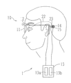
本発明の実施の形態を図面を用いて説明する。図1は視覚再生補助装置の外観を示した概略図、図2は実施の形態で使用する視覚再生補助装置における体内装置を示す図である。視覚再生補助装置1は、外界を撮影するための体外装置10と網膜を構成する細胞に電気刺激を与え、視覚の再生を促す体内装置20とからなる。体外装置10は、患者が掛けるバイザー11と、バイザー11に取り付けられるCCDカメラ等からなる撮影装置12と、外部デバイス13、一次コイルからなる送信手段14等にて構成されている。
Embodiments of the present invention will be described with reference to the drawings. FIG. 1 is a schematic view showing an external appearance of a visual reproduction assisting device, and FIG. 2 is a diagram showing an in-vivo device in the visual reproduction assisting device used in the embodiment. The visual
外部デバイス13には、CPU等の演算処理回路を有するパルス信号変換手段13aと、視覚再生補助装置1(体外装置10及び体内装置20)の電力供給を行うためのバッテリー13bが設けられている。パルス信号変換手段13aは、撮影装置12にて撮影した被写体像を画像処理して、視覚を再生するための電気刺激パルス用データに変換する処理を行う。送信手段14は、パルス信号変換手段13aで変換された電気刺激パルス用データと後述する体内装置20を駆動させるための電力とを電磁波として体内装置20側に伝送(無線送信)する。また、送信手段14の中心には磁石15が取り付けられており、送信手段14によるデータ伝送効率を向上させると共に後述する受信手段23との位置固定に使用される。眼鏡形状のバイザー11は、患者の眼前に装着して使用される。また、バイザー11の前面に取り付けられた撮影装置12によって、患者に視認させる被写体が撮影される。
The
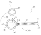
図2(a)に示す体内装置20は、体外装置10からの電磁波を受信する2次コイルからなる受信手段23等からなる受信部20aと、不関電極26と複数の電極27が形成された基板21と電子回路40が搭載された気密ケース100とからなる刺激部20bと、受信部20aと刺激部20b(基板21)とを眼内で接続するためのケーブル22とから構成される。なお、受信手段23には図示なき磁石が配置されており、外部装置10の磁石15の固定に用いられる。
The in-
刺激部20bの電極27は、金、白金等の生体適合性、耐食性に優れた導電性を有する材料にて、基板21に形成された各リード線21aの末端に各々形成される。これにより、各電極27は電子回路40に対して個々に接続される。複数の電極27は、例えば、図2(a)に示すように、基板21の長手方向に沿ってマトリックス状の等間隔に複数個で配置される、又は2次元的に等間隔で互い違いになるように複数個形成され、電極アレイを形成する。電極27の数は、視覚を再生する際の解像度に応じて決定されるが、解像度を高めるためには電極数27は出来るだけ多いことが好ましい。なお、本実施形態では、電極27を十数個〜数百個程度に多く形成されるとする。また、電極の設置スペースや配線技術等に問題がなければ、それ以上の個数があってもよい。
The
基板21はポリイミド等の生体適合性の高い樹脂により所定の厚さで折り曲げ可能に形成される。なお、本実施形態の基板21のベース部は、前述の電極27の形成位置が長板状であると共に、後述する気密ケース100との接合位置が気密ケース100の形状に略一致するように形成されている。なお、気密ケース100との接合位置での基板21の形状は、これに限られるものではなく、気密ケース100全体が搭載できる程度に大きいサイズで形成されていれば良い。
The
基板21上には複数のリード線21aが配線される。基板21の配線は、ベース部に周知のフォトレジスト法、真空蒸着法やスパッタ法等を用いて、耐腐食性の金属材料を蒸着させることによって、図2(a),(b)に示すリード線21aとなる導電層を形成する。導電層の形成後、マスクを取り除き、導電層を被覆するように所定の厚さを有した絶縁層を塗布や貼り付け等により形成する。絶縁層に使用する材料としては、例えば、生体適合性の高いポリイミドやパリレン等の絶縁材料を用いることができる。なお、形成されたリード線21aの末端位置の絶縁層にRIE(reactive ion etching)等の手法によって孔をあけ、リード線21aの末端を露出させ、ここに電極材料を積層(蒸着)し、電極27や電子回路40と基板21との電気的な接合部分を形成する。なお、電極27の数が多いことにより、リード線21aを立体的に複数本配線したい場合は、これらの工程を複数回行うことによって、立体配線を形成することができる。
A plurality of
また、本実施形態では、気密ケース100を眼球に沿わせた曲面形状とするものであるため、基板21においても気密ケース100が取り付けられる領域は、気密ケース100(眼球形状)に合わせた湾曲形状としておく。基板21の所定領域を湾曲形状とする場合には、樹脂基板が熱分解なく変形しやすい温度(例えば、100℃〜300℃程度)にて柔らかくさせた状態にしておき、基板21を所定の曲率(眼球の曲面)を有する型に押し付けることにより湾曲させ成形させる。なお、基板21の成型は熱による劣化を防ぐために、真空雰囲気又は不活性ガスの雰囲気下で行うことが好ましい。
In the present embodiment, since the
電子回路40は、受信手段23にて受信された電磁波に含まれる電気刺激パルス用データと電力とを分ける回路、電気刺激パルス用データを基に視覚を得るための電気刺激パルスとマルチプレクサ制御信号を得るための変換回路、電気刺激パルス信号とマルチプレクサ制御信号とに基づいて、網膜を構成する細胞を刺激する電気刺激パルス(刺激電流)を各電極27から出力させる回路とを有する。なお、電子回路40は、柔軟な素材(ポリイミド等)で形成された周知のフレキシブルプリント基板(以下、単にプリント基板と記す)42に形成される(図3参照)。
The
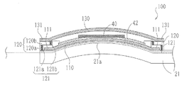
ここで、図3に刺激部20bの気密ケース100付近の断面の模式図を示す。気密ケース100は、一方の面(上面)にプリント基板42が載置され,他方の面(下面)に基板21が接合される載置台110と、載置台110上に載置された電子回路40を密封(ハーメチックシール)するための蓋部材130と、電子回路40と基板21に配設されたリード線21a(電極27)とを電気的に接続するための配線部材120とで構成されている。
Here, the schematic diagram of the cross section of the
載置台110は、眼球の曲面に沿うように所定の曲率半径(例えば、12mm)の曲面を有する円盤形状に形成されている。また、載置台110の外周には平面(平坦)な鍔部111が形成されており、配線部材120の接合面と隙間無く接合することができる。蓋部材130は、載置台110を上方から覆うことのできる大きさであるとともに、載置台110と同様に眼球に沿う曲率半径の曲面を有する円盤形状に形成されている。また蓋部材110の外周は平面(平坦)な鍔部131が形成され、配線部材120の接合面と隙間無く接合することができる。このように、載置台110及び蓋部材130が眼球形状に沿った曲面形状に形成されることで、眼球に沿って好適に基板21を設置することができる。
The mounting table 110 is formed in a disk shape having a curved surface with a predetermined radius of curvature (for example, 12 mm) along the curved surface of the eyeball. In addition, a flat (flat)
載置台110と蓋部材130とは、生体適合性を有し気密性が高い金属材料にて形成される。例えば、チタン、チタン合金(例えば、チタンアルミニウム合金、チタンバリウム合金等)、ステンレス、白金、金等により形成される。このような金属材料を使用することにより、必要とされる強度を保ちつつ各部材の厚さを例えば、0.1mmから0.4mm程度に薄く形成することができる。なお、このような金属材料を用いて載置台110及び蓋部材130が持つ曲面形状を形成する場合には、周知の板金加工、プレス加工等の方法を用いればよい。
The mounting table 110 and the
配線部材120は、絶縁性及びガスや水分に対する気密性とを有する(透過性が低い)と共に、生体適合性を有する酸化物セラミックス(例えば、アルミナ)で形成される。これ以外にも、配線部材120はガラスセラミックス等のセラミックス材料にて形成しても良い。なお、配線部材120には、気密ケース100内部に置かれた電子回路40が持つパターン配線の端子と、気密ケース100外部に配線されている各リード線21a(電極27)とを電気的に接続するための複数の導通部材121が、配線部材120の形状に沿って所定の間隔ごとに(隣合う導通部材121同士が重ならないように)形成される。なお、詳細な説明は後述するが、導通部材121は、ビア121a及びビア120bと、ビア121aと120bとを電気的に接続するために配線部材120の内部に形成される導電層(図示は省略する)とから構成される(図3参照)。また、配線部材120は載置台110の外周部分と蓋部材130の外周部分との間に接合されるものであり、載置台110と蓋部材130の外周に沿うように、例えば、環状に形成される。
The
ここで、配線部材120の形成方法を説明する。配線部材120はファインセラミックス(ニューセラミックス)の既存の成型技術により作製することができる。はじめに、アルミナの粉末を用いて板状の層(グリーンシート)を形成する。そして、ビア121aとビア121bとを接続する導電層を形成するために、グリーンシートの表面に導電材料によるペーストを周知の方法にて印刷する。次に、グリーンシートを周知のレーザ照射等により切削加工して複数の環状の層を得る。そして、各環状の層の肉厚方向に、ビア121a、121bを形成するための複数の貫通孔を形成させる。貫通孔は、パンチ、マイクロドリル、レーザ照射等で形成することができる。ここでは、直径約100〜200μmの複数の貫通孔が環状形状に沿って形成される。次に、複数枚の環状の層の貫通孔が一致されるように積み重ねて、載置台120に接続される側の層120aと蓋部材130に接続される側の層120bとを形成させる。なお、本実施形態では、層120aと層120bを一旦別々に形成した後に、一体化させて配線部材120全体を形成することとする(図3参照)。その為、層120aと層120bの接続面の少なくとも一方には前述の導電層が位置されるようにする。なお、層120aを形成するときに、内径が異なる環状の層を使用することで、載置台110の鍔部111に嵌合する溝が形成される。
Here, a method of forming the
また、層120aと層120bに形成された貫通孔は、層120aと層120bとの一体化により配線部材120が形成されたときに、対応するビア121aとビア121bとが接続されるような数及び位置に形成されれば良い。なお、このとき、前述の導電層が対応する貫通孔が接続されるような形状に印刷されていることによって、ビア121aとビア121bとが電気的に接続されるようになる。
The number of through holes formed in the
なお、本実施形態では、層120aに形成される貫通孔は、溝と鍔部111とが嵌合された時に、ビア121aの一端が基板21側(気密ケース100の外側)となる位置に形成される。一方、層120bに形成される貫通孔は、蓋部材130と配線部材120とが接続されたときに、ビア121bの一端が載置台110と蓋部材130とで形成される空間(気密ケース100の内側)に位置されるように形成される。これにより、電子回路40の端子とビア121bとが、導通部材121を介して電気的に接続されるようになる(図3参照)。
In the present embodiment, the through hole formed in the
次に、貫通孔にビア121a及びビア121bを形成するための導電材料を充填させる。導電材料としては、銀、タングステン又はモリブデン等を1種または複数混合した周知のものが基材として用いられる。貫通孔に導電材料を充填させたら、層120aと層120bの対応する貫通孔同士が導電層を介して電気的に接続されるように、層120aと層120bとを置き合わせる。そして、周知の炉による高温加熱による焼成により焼き固める。これにより、内部に導通部材121を有する配線部材120が形成される。
Next, the through hole is filled with a conductive material for forming the via 121a and the via 121b. As the conductive material, a known material in which one or a plurality of silver, tungsten, molybdenum, or the like is mixed is used as the base material. When the through hole is filled with the conductive material, the
以上のように、本実施形態では、周知の方法を用いて、平面の(平坦な)配線部材120が容易に形成されると共に、所期の数の導通部材121を形成することができる。また、詳細な説明は後述するが、配線部材120が平らに形成することで、電子回路40とリード線21aとを従来と同じ方法(フリップチップ実装)にて簡単に接続させることができるようになる。
As described above, in this embodiment, the planar (flat)
次に、以上のような構成を備える気密ケース100を備える刺激部20bの形成方法を説明する。図4は刺激部20bの作成方法の説明図である。まず、図4(a)に示すように、電子回路40が組み込まれたプリント基板42を、載置台110に搭載させる。このとき、柔軟なプリント基板42は載置台110の曲面に沿って曲がり、電子回路40はこれに追従して位置されるようになる。次に、図4(b)に示すように、配線部材120に形成された溝を、載置台110の鍔部111に嵌合させる。そして、この状態で、電子回路40端子部分(プリント基板42の端子部分)と、載置台110と蓋部材130とで形成される空間側に位置される導通部材121の端面とを(直接又は間接的に)半田付け等の周知の溶接方法により接続させる。これにより、導通部材121と電子回路40とがプリント基板42を介して電気的に接続される。
Next, the formation method of the
次に、図4(c)に示すように、配線部材120の上面に蓋部材130を取り付ける。そして、載置台110と配線部材120、蓋部材130と配線部材120とをそれぞれ接合させる。ここでは、各部材の接続位置を図示を略すローラにて加熱、加圧しながらなぞることで、シーム接合(溶接)させるとする。なお、各部材の接続は不活性ガス(アルゴンや窒素ガス)雰囲気下で行うとする。例えば、不活性ガスとしてはアルゴンが用いられる。これにより、気密ケース100の内部空間がアルゴンで充填された状態となる。
Next, as shown in FIG. 4C, the
以上のような各部材の接合により、電子回路40のハーメチックシール用の気密ケース100が形成され、電子回路40が密封されて外部から保護されるようになる。なお、図示は省略するが、配線部材120の導通部材121とケーブル22とを接合させる。ケーブル22の先端を導通部材121に当接させ、高温高圧下で接合させる。金属同士のケーブル22と導通部材121は強固に接合される。
By joining the respective members as described above, the
次に、気密ケース100の外部に位置される導通部材121の端部に、既存技術を用いて金等の生体適合性を有する金属によりバンプ122を形成させる。そして、図4(d)に示すように、各バンプ122と基板21上に形成されたリード線21aの露出部分(端部)を位置合わせして当接させる。このとき、基板21が気密ケース100の形状に沿うような曲面に形成されていることで、気密ケース100と基板21とが密着して接合されやすい。その後、各バンプ122とリード線21とを周知のフリップチップ実装による溶接で電気的に接続させる。なお、気密ケース100と基板21との間隙は、生体適合性を有するエポキシ樹脂にて充填することにより埋める事ができる。なお、気密ケース100と基板21との接合では、バンプ122を気密ケース100側に形成する構成としたが、これに限るものではない。基板21の露出するリード線21a上にバンプを形成する構成としてもよい。
Next, bumps 122 are formed on the end portion of the
以上の一連の接合後、電極27以外の気密ケース100及び基板21全体を、生体適合性の高い樹脂(シリコーン、パリレン、生体適合性の高いポリイミド等)で包埋する。樹脂による包埋によって、気密ケース100と基板21とが一体化されると共に、電子回路40が好適に密封されるようになる。
After the above series of joining, the entire
以上のような構成を備える体内装置20は、図5に示すように、電極27が形成された基板21の一部が患者眼Eの強膜E3に作製された強膜ポケットに位置される。一方、残りの基板21の部分と気密ケース100とは眼球(強膜)の曲面に沿って配置される。これにより、刺激部20b全体が眼内で安定して設置されることとなる。なお、本実施形態では、強膜側(脈絡膜側)から網膜E1を構成する細胞を電気刺激する構成としたが、これに限るものではない。患者眼の網膜を構成する細胞を好適に刺激することが可能な位置に電極を設置することができればよい。例えば、体内装置を患者眼Eの眼内(網膜上や網膜下)に置き、電極が形成されている基板先端部分を網膜下(網膜と脈絡膜との間)や網膜上に設置させるような構成とすることもできる。この場合には気密ケースやこれを載置する基板部分の形状を網膜の曲面に沿う形状としておけばよい。なお、基板21は、例えばタックや生体適合性の高い接着剤等にて強膜E3に固定保持させても良い。同様に、気密ケース100も縫合等で取付け位置を固定することで、より眼内に安定して位置させるようにしても良い。
In the
次に、以上のような構成を備える視覚再生補助装置の視覚再生のための動作を、図6に示す制御系のブロック図を基に説明する。撮影装置12で撮影された被写体の撮影データ(画像データ)は、パルス信号変換手段13aに送られる。パルス信号変換手段13aは、撮影した被写体を患者が視認するために必要となる所定の帯域内の信号(電気刺激パルス用データ)に変換し、送信手段14より電磁波として体内装置20側に送信する。同時に、パルス信号変換手段13aは、バッテリー13bから供給される電力を前述した信号(電気刺激パルス用データ)の帯域と異なる帯域の信号(電力)に変換し、電磁波として電気刺激パルス用データと合わせて体内装置20側に送信する。体内装置20側では、体外装置10より送られてくる電気刺激パルス用データと電力とを受信手段23で受信し、電子回路40に送る。電子回路40では受信信号から、電気刺激パルス用データが使用する帯域の信号を抽出する。また、電子回路40は、抽出した電気刺激パルス用データに基づいて、各電極27に分配される電気刺激パルスと、電気刺激パルスの分配を制御するマルチプレクサ制御信号とを生成し、電気刺激パルスを複数の各電極27へと分配し、電気刺激パルス(刺激電流)を各電極27から出力させる。各電極27から出力される電気刺激パルスによって網膜を構成する細胞が刺激され、患者は視覚を得る。なお、以上のような構成によって、より多くの電極27が基板21上に形成されることで、患者の網膜がより精度良く刺激されるようになる。
Next, an operation for visual reproduction of the visual reproduction auxiliary device having the above-described configuration will be described based on the block diagram of the control system shown in FIG. The photographing data (image data) of the subject photographed by the photographing
以上のように、気密ケース100の設置面が、眼内の曲面に沿うような曲率半径を有する形状に形成されることで、気密ケース100の大きさに関わらず、刺激部20b全体が眼内で好適に位置され、長期間安定して使用することができるようになる。
As described above, the installation surface of the
なお、本実施形態では、気密ケース100が所定の曲率半径を有する円盤状に形成される場合を例に挙げて説明したが、これに限られるものではない。例えば、図7の刺激部20bの変用例に示すように、気密ケース100は、眼内に沿う方向に所定の曲率半径を有する曲面を備えていれば長方形状に形成されていても良い。この場合、基板21も気密ケース100の形状に合わせた長方形状に形成される。このようにすると、電極27の数に応じて、眼内での刺激部20bの設置面積を少なくでき、より患者の負担を軽減することができるようになる。
In the present embodiment, the case where the
また、図8の刺激部20bの変用例2に示すように、導通部材121は配線部材120の形状に沿って、複数列で形成されていても良い。このようにすると、より多くの導通部材121が形成されることで、更に電極27の数を増加させる場合にも対応できるようになる。なお、この場合の各導通部材121は、その形成位置が重ならないような位置に形成されれば良い。
In addition, as shown in the second modification of the
なお、上記構成の体内装置20では、参照電極26は刺激部20bに一体的に形成されているが、これに限るものではない。例えば、金属の蓋部材130の被膜の一部を取り除き、この露出部分を参照電極26として使用しても良い。この場合には、参照電極26として使用される蓋部材130(気密ケース100)は、電極27と導通されるように体内装置に取り付けられていれば良い。また、上記の実施例では受信手段23(受信部20a)と刺激部20bとがケーブル22を介して接続される場合が示されているが、受信部20bと刺激部20bとはケーブル22を介さずに直接接続されていても良い。この場合、気密ケース100の少なくとも2つの導通部材121と受信部20bとが接続されれば良い。このようにすると、より体内装置20の形状を小さくでき、更に患者の負担を減らすことができるようになる。
In the in-
1 視覚再生補助装置
21 基板
21a リード線
27 電極
40 電子回路
100 気密ケース
110 載置台
120 配線部材
121 導通部材
130 蓋部材
DESCRIPTION OF
Claims (4)
網膜を構成する細胞に電気刺激を与えるための複数の刺激電極と該複数の電極の各々に接続されるリード線とが形成される基板であって,眼球形状に沿う曲率半径を有した曲面形状を持つ基板と、
前記刺激電極に送る電気刺激パルスを制御するための電子回路と、
生体適合性を有する金属材料にて形成され前記電子回路を上面側に載置し下面側を前記基板に接合される載置台であって,少なくとも下面が眼球の曲面形状に沿った形状を持つ載置台と、
生体適合性を有する金属材料にて眼内の曲面形状に沿う曲率半径で形成されると共に前記載置台に載置された前記電子回路を密封するための蓋部材と、
生体適合性及び絶縁性を有する材料にて前記載置台及び前記蓋部材の外周に沿って輪状に形成された配線部材であって、前記リード線と前記電子回路とを電気的に接続するための導通部材が形成された配線部材と、を備え、
前記載置台及び前記蓋部材の外周部分と前記配線部材との接合により構成される気密ケースによって前記電子回路がハーメチックシールされることを特徴とする視覚再生補助装置。 In a visual reproduction assisting device that reproduces the vision of a patient
A substrate on which a plurality of stimulation electrodes for applying electrical stimulation to cells constituting the retina and lead wires connected to each of the plurality of electrodes are formed, and a curved surface shape having a radius of curvature along the eyeball shape A substrate with
An electronic circuit for controlling an electrical stimulation pulse to be sent to the stimulation electrode;
A mounting table formed of a metal material having biocompatibility and mounting the electronic circuit on the upper surface side and bonding the lower surface side to the substrate, at least the lower surface having a shape along the curved shape of the eyeball. A table,
A lid member for sealing the electronic circuit formed on the mounting table and formed with a radius of curvature along the curved surface shape in the eye with a metal material having biocompatibility;
A wiring member formed in a ring shape along the outer periphery of the mounting table and the lid member with a material having biocompatibility and insulation, for electrically connecting the lead wire and the electronic circuit A wiring member having a conductive member formed thereon,
The visual reproduction assisting device, wherein the electronic circuit is hermetically sealed by an airtight case configured by joining the mounting table and the outer peripheral portion of the lid member and the wiring member.
前記載置台及び蓋部材はチタン又はチタン合金又はステンレスにて形成されていることを特徴とする視覚再生補助装置。 The visual reproduction assisting device according to claim 1, wherein
A visual reproduction assisting device, wherein the mounting table and the lid member are made of titanium, a titanium alloy, or stainless steel.
前記配線部材はセラミックスにて形成されていることを特徴とする視覚再生補助装置。 The visual reproduction assisting device according to claim 2, wherein
The visual reproduction assisting device, wherein the wiring member is made of ceramics.
前記配線部材における前記設置台及び前記蓋部材との接合面は平面に形成されており、
前記設置台及び前記蓋部材の外周には,前記配線部材の前記接合面と接合させるために平面の鍔部が形成されていることを特徴とする視覚再生補助装置。 In the visual reproduction auxiliary device according to claims 1 to 3,
The joint surface between the installation base and the lid member in the wiring member is formed in a plane,
A visual regeneration assisting device, wherein a flat collar portion is formed on the outer periphery of the installation base and the lid member so as to be joined to the joining surface of the wiring member.
Priority Applications (1)
| Application Number | Priority Date | Filing Date | Title |
|---|---|---|---|
| JP2010026941A JP2011160984A (en) | 2010-02-09 | 2010-02-09 | Visual sense regeneration assisting apparatus |
Applications Claiming Priority (1)
| Application Number | Priority Date | Filing Date | Title |
|---|---|---|---|
| JP2010026941A JP2011160984A (en) | 2010-02-09 | 2010-02-09 | Visual sense regeneration assisting apparatus |
Publications (2)
| Publication Number | Publication Date |
|---|---|
| JP2011160984A true JP2011160984A (en) | 2011-08-25 |
| JP2011160984A5 JP2011160984A5 (en) | 2013-03-28 |
Family
ID=44592372
Family Applications (1)
| Application Number | Title | Priority Date | Filing Date |
|---|---|---|---|
| JP2010026941A Pending JP2011160984A (en) | 2010-02-09 | 2010-02-09 | Visual sense regeneration assisting apparatus |
Country Status (1)
| Country | Link |
|---|---|
| JP (1) | JP2011160984A (en) |
Cited By (3)
| Publication number | Priority date | Publication date | Assignee | Title |
|---|---|---|---|---|
| CN103690300A (en) * | 2013-12-19 | 2014-04-02 | 中国医学科学院生物医学工程研究所 | Retinal prosthesis with spherical arc substrate |
| JP2014076193A (en) * | 2012-10-11 | 2014-05-01 | Nidek Co Ltd | Visual sense regeneration assisting apparatus |
| JP2015070976A (en) * | 2013-10-04 | 2015-04-16 | 株式会社ニデック | Visual sense regeneration auxiliary device |
Citations (5)
| Publication number | Priority date | Publication date | Assignee | Title |
|---|---|---|---|---|
| JP2004298299A (en) * | 2003-03-31 | 2004-10-28 | Nidek Co Ltd | Visual sense regeneration auxiliary device |
| JP2006051164A (en) * | 2004-08-11 | 2006-02-23 | Seiko Epson Corp | Artificial retina and method for manufacturing the same |
| JP2007503265A (en) * | 2003-08-26 | 2007-02-22 | ヴィスタ サイエンティフィック エルエルシー | Ophthalmic drug supply device |
| JP2008055000A (en) * | 2006-08-31 | 2008-03-13 | Nidek Co Ltd | Visual regeneration device |
| US20090118805A1 (en) * | 2007-07-05 | 2009-05-07 | Greenberg Robert J | Return Electrode for a Flexible Circuit Electrode Array |
-
2010
- 2010-02-09 JP JP2010026941A patent/JP2011160984A/en active Pending
Patent Citations (5)
| Publication number | Priority date | Publication date | Assignee | Title |
|---|---|---|---|---|
| JP2004298299A (en) * | 2003-03-31 | 2004-10-28 | Nidek Co Ltd | Visual sense regeneration auxiliary device |
| JP2007503265A (en) * | 2003-08-26 | 2007-02-22 | ヴィスタ サイエンティフィック エルエルシー | Ophthalmic drug supply device |
| JP2006051164A (en) * | 2004-08-11 | 2006-02-23 | Seiko Epson Corp | Artificial retina and method for manufacturing the same |
| JP2008055000A (en) * | 2006-08-31 | 2008-03-13 | Nidek Co Ltd | Visual regeneration device |
| US20090118805A1 (en) * | 2007-07-05 | 2009-05-07 | Greenberg Robert J | Return Electrode for a Flexible Circuit Electrode Array |
Cited By (3)
| Publication number | Priority date | Publication date | Assignee | Title |
|---|---|---|---|---|
| JP2014076193A (en) * | 2012-10-11 | 2014-05-01 | Nidek Co Ltd | Visual sense regeneration assisting apparatus |
| JP2015070976A (en) * | 2013-10-04 | 2015-04-16 | 株式会社ニデック | Visual sense regeneration auxiliary device |
| CN103690300A (en) * | 2013-12-19 | 2014-04-02 | 中国医学科学院生物医学工程研究所 | Retinal prosthesis with spherical arc substrate |
Similar Documents
| Publication | Publication Date | Title |
|---|---|---|
| JP2008055000A (en) | Visual regeneration device | |
| JP2007044323A (en) | Eyesight regeneration supporting apparatus | |
| US10500393B2 (en) | Liquid crystal polymer-based electrode array and package for neural implant, and manufacturing method therefor | |
| US9174047B2 (en) | Electrical feedthrough assembly | |
| US11529524B2 (en) | Encapsulated electronic circuit | |
| US20160086824A1 (en) | Bio-implantable hermetic integrated ultra high density device | |
| JP4412924B2 (en) | Visual reproduction assist device | |
| JP5501745B2 (en) | Visual reproduction assist device | |
| JP2011160984A (en) | Visual sense regeneration assisting apparatus | |
| US20170203108A1 (en) | Electrical Feedthrough Assembly | |
| JP2010172667A (en) | Hermetic sealing method for electronic element, functional device unit for biological implantation using the method, and visual restoration aiding apparatus | |
| JP6357752B2 (en) | Manufacturing method of visual reproduction assist device | |
| JP2006280412A (en) | Auxiliary device for regenerating visual sense and method of manufacturing | |
| JP5122244B2 (en) | Visual reproduction assist device | |
| JP4359567B2 (en) | Visual reproduction assist device and method of manufacturing the same | |
| JP5219443B2 (en) | Method for producing stimulation unit for visual reproduction assist device | |
| JP5265209B2 (en) | Visual reproduction assist device | |
| US20150100111A1 (en) | Vision restoration assist apparatus | |
| JP2009082496A (en) | Sight regeneration aid | |
| KR100619103B1 (en) | An implant package for prosthetic cochleas and a method for manufacturing the same | |
| JP4994667B2 (en) | Visual reproduction assist device | |
| JP2008245834A (en) | Vision regeneration assisting device, and conducting wire connecting method of vision regeneration assisting device | |
| JP2015106430A (en) | Feedthrough |
Legal Events
| Date | Code | Title | Description |
|---|---|---|---|
| A521 | Written amendment |
Free format text: JAPANESE INTERMEDIATE CODE: A523 Effective date: 20130208 |
|
| A621 | Written request for application examination |
Free format text: JAPANESE INTERMEDIATE CODE: A621 Effective date: 20130208 |
|
| A131 | Notification of reasons for refusal |
Free format text: JAPANESE INTERMEDIATE CODE: A131 Effective date: 20131127 |
|
| A977 | Report on retrieval |
Free format text: JAPANESE INTERMEDIATE CODE: A971007 Effective date: 20131129 |
|
| A521 | Written amendment |
Free format text: JAPANESE INTERMEDIATE CODE: A523 Effective date: 20140127 |
|
| A131 | Notification of reasons for refusal |
Free format text: JAPANESE INTERMEDIATE CODE: A131 Effective date: 20140305 |
|
| A02 | Decision of refusal |
Free format text: JAPANESE INTERMEDIATE CODE: A02 Effective date: 20140709 |