JP2011124258A - Nitride-based diode - Google Patents
Nitride-based diode Download PDFInfo
- Publication number
- JP2011124258A JP2011124258A JP2009278331A JP2009278331A JP2011124258A JP 2011124258 A JP2011124258 A JP 2011124258A JP 2009278331 A JP2009278331 A JP 2009278331A JP 2009278331 A JP2009278331 A JP 2009278331A JP 2011124258 A JP2011124258 A JP 2011124258A
- Authority
- JP
- Japan
- Prior art keywords
- nitride
- mesa
- anode electrode
- diode
- electrode
- Prior art date
- Legal status (The legal status is an assumption and is not a legal conclusion. Google has not performed a legal analysis and makes no representation as to the accuracy of the status listed.)
- Granted
Links
Images


Abstract
Description
本発明は、窒化物系ショットキーバリアダイオードなどの窒化物系ダイオードに関する。 The present invention relates to a nitride-based diode such as a nitride-based Schottky barrier diode.
III族窒化物系化合物半導体に代表されるワイドバンドギャップ半導体は、高い絶縁破壊耐圧、良好な電子輸送特性、良好な熱伝導度を持つので、高温、大パワー、あるいは高周波用半導体デバイスの材料として非常に魅力的である。
例えば、III族窒化物系化合物半導体である窒化ガリウム(GaN)は、GaAs系の材料に比べてそのバンドギャップエネルギーが大きいため、絶縁破壊電圧が高く、しかも耐熱温度が高く高温動作に優れているので、これらの材料、とくにGaN/AlGaN系半導体を用いた電界効果トランジスタ(Field Effect Transistor:FET)やパワースイッチング用ダイオードの開発が進められている。
Wide band gap semiconductors typified by Group III nitride compound semiconductors have high dielectric breakdown voltage, good electron transport properties, and good thermal conductivity, so they can be used as semiconductor devices for high temperature, high power, or high frequency applications. Very attractive.
For example, gallium nitride (GaN), which is a group III nitride compound semiconductor, has a higher bandgap energy than a GaAs material, and therefore has a high dielectric breakdown voltage, a high heat resistance temperature, and high temperature operation. Therefore, development of field effect transistors (FETs) and power switching diodes using these materials, particularly GaN / AlGaN-based semiconductors, is in progress.
その一例としてショットキーバリアダイオード(SBD)を図14に示した。図14に示すSBD100は、図示を省略した基板上に、キャリアがドリフトする導電性のGaN系半導体からなるチャネル層101と、AlGaN系半導体からなる電子供給層102とが形成され、電子供給層102上に、オーミック電極103とショットキー電極104とが絶縁膜105を介して配置されたGaN系ダイオードである。ショットキー電極104はNiやPtなどの金属を含む積層構造からなり、オーミック電極103はTiおよびAlなどの金属を含む積層構造からなる。このSBD100は、電子供給層102とのヘテロ接合界面に二次元電子ガス層106が形成されたチャネル層101を用いて、ショットキー電極104をアノード電極にし、オーミック電極103をカソード電極にしている。
As an example, a Schottky barrier diode (SBD) is shown in FIG. In the SBD 100 shown in FIG. 14, a
図14に示すSBD100のようにAlGaN/GaNヘテロ構造を有する窒化物系ダイオードでは、チャネル層101と電子供給層102の界面に、ピエゾ効果によって、チャネル層101側に2次元電子ガス層106が形成されている。この2次元電子ガス層106は、高い電子移動度とキャリア密度を有しているため、AlGaN/GaNヘテロ構造を用いたヘテロ接合窒化物系ダイオードでは、低いオン抵抗、および速いスイッチング速度での動作が可能である。これらの特徴は、パワースイッチング応用に非常に好適である。
上述したAlGaN/GaNヘテロ構造を有するショットキーバリアダイオードとして、例えば、特許文献1及び非特許文献1等に開示されたものが知られている。
In a nitride-based diode having an AlGaN / GaN heterostructure like the SBD 100 shown in FIG. 14, a two-dimensional
As the Schottky barrier diode having the AlGaN / GaN heterostructure described above, for example, those disclosed in Patent Document 1, Non-Patent Document 1, and the like are known.
近年、高電子移動度トランジスタ(HEMT)構造を有効に活用し、ダイオードとして動作させる構造が考えられている。しかし、図14に示す上記従来のSBD100では、オン特性は良いものの、本質的にピンチオフ電圧までは逆方向リーク電流が増大するため、結果としてリークが大きくなっていた。また、そのため耐圧が十分に確保できない問題点もあった。
そこで、本発明が解決しようとする課題は、高耐圧でかつ低オン電圧動作が可能な窒化物系ダイオードを提供するものである。
In recent years, a structure in which a high electron mobility transistor (HEMT) structure is effectively used to operate as a diode has been considered. However, although the above-described
Therefore, the problem to be solved by the present invention is to provide a nitride-based diode capable of operating at a high breakdown voltage and a low on-voltage.
上記課題を解決するために、請求項1に記載の発明に係る窒化物系ダイオードは、基板上に形成された第1の窒化物系化合物半導体からなるチャネル層と、前記チャネル層上に形成され、第2の窒化物系化合物半導体からなる電子供給層と、前記電子供給層上に形成されたカソード電極およびアノード電極と、前記電子供給層の一部を、前記チャネル層に達する深さまで部分的に除去したメサと、を備え、前記メサの側面部に、前記カソード電極およびアノード電極のうち、少なくとも前記アノード電極が接触していることを特徴とする。 In order to solve the above-described problem, a nitride-based diode according to the invention described in claim 1 is formed on a channel layer made of a first nitride-based compound semiconductor formed on a substrate, and on the channel layer. , An electron supply layer made of a second nitride-based compound semiconductor, a cathode electrode and an anode electrode formed on the electron supply layer, and a part of the electron supply layer partially to a depth reaching the channel layer And at least the anode electrode of the cathode electrode and the anode electrode is in contact with the side surface of the mesa.
請求項2に記載の発明に係る窒化物系ダイオードは、前記メサの上面に絶縁膜が形成され、前記アノード電極が前記絶縁膜上から前記メサの側面部にわたって形成されていることを特徴とする。
The nitride-based diode according to
請求項3に記載の発明に係る窒化物系ダイオードは、前記カソード電極および前記アノード電極は、フィンガー部を有し、前記メサが前記フィンガー部の長手方向に沿って間欠的に形成されていることを特徴とする。 In the nitride-based diode according to the third aspect of the present invention, the cathode electrode and the anode electrode have finger portions, and the mesa is intermittently formed along the longitudinal direction of the finger portions. It is characterized by.
請求項4に記載の発明に係る窒化物系ダイオードは、前記メサは、前記カソード電極または前記アノード電極と前記メサの各側面部とが接触する面積が、前記フィンガー部の先端側へ向かって徐々に大きくなるように形成されていることを特徴とする。 In the nitride-based diode according to claim 4, the mesa has an area where the cathode electrode or the anode electrode and each side surface of the mesa contact each other gradually toward the tip side of the finger portion. It is characterized by being formed so as to be larger.
請求項5に記載の発明に係る窒化物系ダイオードは、前記第1のGaN系半導体材料はGaNであり、前記第2のGaN系半導体材料はAlGaNであることを特徴とする。 The nitride diode according to the invention of claim 5 is characterized in that the first GaN-based semiconductor material is GaN and the second GaN-based semiconductor material is AlGaN.
請求項6に記載の発明に係る窒化物系ダイオードは、前記第1のGaN系半導体材料はInGaN或いはGaNであり、前記第2のGaN系半導体材料はInAlGaNであることを特徴とする。 The nitride-based diode according to the invention of claim 6 is characterized in that the first GaN-based semiconductor material is InGaN or GaN, and the second GaN-based semiconductor material is InAlGaN.
請求項7に記載の発明に係る窒化物系ダイオードは、前記アノード電極には、Ni、Pt、Pd、W、TaおよびAl、またはそれらの金属の合金を用いることを特徴とする。 The nitride-based diode according to the invention described in claim 7 is characterized in that Ni, Pt, Pd, W, Ta and Al, or an alloy of these metals is used for the anode electrode.
請求項8に記載の発明に係る窒化物系ダイオードは、前記カソード電極には、Ti、Al、Si、Ta、W、Mo、またはそれらの合金を用いることを特徴とする。 The nitride-based diode according to an eighth aspect of the invention is characterized in that Ti, Al, Si, Ta, W, Mo, or an alloy thereof is used for the cathode electrode.
請求項9に記載の発明に係る窒化物系ダイオードは、前記基板は導電性の基板であり、前記カソード電極またはアノード電極は前記基板の裏面に形成した裏面電極に電気的に接続されていることを特徴とする。 In the nitride-based diode according to claim 9, the substrate is a conductive substrate, and the cathode electrode or the anode electrode is electrically connected to a back electrode formed on the back surface of the substrate. It is characterized by.
請求項1に記載の発明によれば、カソード電極およびアノード電極のうち、少なくともアノード電極が、メサの側面部においてチャネル層(2次元電子ガス層)と接触している。これにより、電子供給層においてトンネル電流が生じることがないので、逆方向のリーク電流が低減される。これによって高耐圧でかつ低オン電圧動作が可能な窒化物系ダイオードを実現することができる。 According to the first aspect of the present invention, at least the anode electrode of the cathode electrode and the anode electrode is in contact with the channel layer (two-dimensional electron gas layer) at the side surface of the mesa. Thereby, since no tunnel current is generated in the electron supply layer, the reverse leakage current is reduced. As a result, it is possible to realize a nitride-based diode that can operate at a high breakdown voltage and a low on-voltage.
請求項2に記載の発明によれば、アノード電極が電子供給層のメサ上面に接触する面積を極力低減させて、アノード電極をメサの側面部に接触させた構造になっているので、リーク電流が更に低減され、これによって、耐圧が更に向上する。 According to the second aspect of the present invention, the anode electrode is in contact with the side surface of the mesa by reducing the area where the anode electrode is in contact with the mesa upper surface of the electron supply layer as much as possible. Is further reduced, whereby the breakdown voltage is further improved.
請求項4に記載の発明によれば、フィンガー部を有するアノード電極の端部での電界集中が緩和され、更に高耐圧のダイオードが実現できる。 According to the fourth aspect of the present invention, the electric field concentration at the end of the anode electrode having the finger portion is alleviated, and a diode having a higher breakdown voltage can be realized.
以下に、本発明に係る窒化物系ダイオードの実施の形態を図面に基づいて説明する。なお、各実施の形態の説明において同様の部位には同一の符号を付して重複した説明を省略する。 Embodiments of a nitride diode according to the present invention will be described below with reference to the drawings. In the description of each embodiment, the same parts are denoted by the same reference numerals, and redundant description is omitted.
(第1の実施形態)
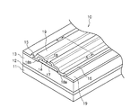
図1は、本発明の第1の実施形態に係る窒化物系ダイオードの概略構成を示している。
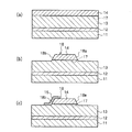
本実施形態に係る窒化物系ダイオードは、一例としてAlGaN/GaNヘテロ接合構造を有する窒化物系ショットキーバリアダイオードとして構成されている。 この窒化物系ダイオード10は、図1に示すように、シリコン(111)基板11と、シリコン基板11の(111)面上に形成されたバッファ層12と、バッファ層12上に形成されたアンドープのGaN(第1の窒化物系化合物半導体)からなるチャネル層13と、チャネル13層上に形成されたアンドープのAlGaN(第2の窒化物系化合物半導体)からなる電子供給層14と、電子供給層14上に形成されたカソード電極15およびアノード電極16とを備えている。
(First embodiment)
FIG. 1 shows a schematic configuration of a nitride-based diode according to the first embodiment of the present invention.
The nitride diode according to the present embodiment is configured as a nitride Schottky barrier diode having an AlGaN / GaN heterojunction structure as an example. As shown in FIG. 1, the nitride-based
このようなAlGaN/GaNヘテロ接合構造を有する窒化物系ダイオード10では、チャネル層13と電子供給層14の界面、つまり、AlGaN/GaNヘテロ接合界面にピエゾ効果によって、チャネル層13側に2次元電子ガス層17が発生している。この窒化物系ダイオード10では、高キャリア濃度の2次元電子ガス層17が形成されたチャネル層13を用いて、カソード電極15をオーミック電極にし、アノード電極16をショットキー電極にしている。
In the nitride-based
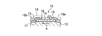
窒化物系ダイオード10は、さらに、図1および図2に示すように、電子供給層14の一部を、チャネル層13に達する深さまで部分的に除去したメサ18を備え、メサ18の一方の側面部18aにアノード電極16が接触している。つまり、電子供給層14のうち、アノード電極を形成する領域を、チャネル層13に達する深さまで部分的にエッチングにより除去することで露出したチャネル層13の表面の一部(メサ18の側面部18aおよびメサ18の上面の一部)にアノード電極16が形成されている。アノード電極16がメサ18の側面部18aに接触することで、アノード電極16と2次元電子ガス層17とが電気的に接続されている。
As shown in FIGS. 1 and 2, the nitride-based
また、メサ18のもう一方の側面部18bには、カソード電極15が接触している。つまり、電子供給層14のうち、カソード電極15を形成する領域を、チャネル層13に達する深さまで部分的にエッチングにより除去することで露出したチャネル層13の表面の一部(メサ18の側面部18bおよびメサ18の上面の一部)にカソード電極15が形成されている。さらに、窒化物系ダイオード10は、カソード電極15とアノード電極16を絶縁するように、チャネル層13および電子供給層14の表面に形成されたSiO2等からなる絶縁膜19を備えている。
The
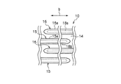
図3は、窒化物系ダイオード10を上方から見た図で、各電極の配置を説明するための模式図である。図4は、図2のA−A線に沿った断面図である。
図1で説明した窒化物系ダイオード10では、図2および図3に示すように、大電流性能を得るために長尺化する必要があるため、カソード電極15およびアノード電極16は、チャネル層13を電流が流れる方向a(図4参照)に対して垂直な方向b(図3参照)に長いフィンガー形状に形成され、カソード電極15とアノード電極16が交互に配置された櫛状の電極になっている。つまり、カソード電極15およびアノード電極16はフィンガー部15aおよび16aをそれぞれ有する(図3参照)。このような櫛状の電極構成に対応して、メサ18の側面部18a、18bは、図2および図3の破線で示すように、上記方向bに細長い形状になっている。メサ18の側面部18aには、フィンガー形状のアノード電極16の中心部全体(フィンガー部16aの中心部全体)が接触している(図2、図3参照)。一方、メサ18の側面部18bには、フィンガー形状のカソード電極15の中心部全体(フィンガー部15aの中心部全体)が接触している(図2、図3参照)。
FIG. 3 is a view of the nitride-based
In the nitride-based
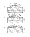
図1に示す窒化物系ダイオード10は以下のようにして作製することが可能である。即ち、成長装置はMOCVD(Metal Organic Chemical Vapor Deposition)装置を用い、基板は、シリコン(111)基板11を用いた。
The nitride-based
(工程1)
シリコン基板11の(111)面上にバッファ層12を形成する。(工程1)では、まず、シリコン基板11をMOCVD装置内に導入し、ターボポンプでMOCVD装置内の真空度を1×10⁻⁶hPa以下になるまで真空引きした後、真空度を100hPaとし、基板11を1000℃に昇温した。温度が安定したところで、シリコン基板11を900rpmで回転させ、原料となるトリメチルアルミニウム(TMA)を100cm3/min、アンモニアを12リットル/minの流量でシリコン基板11の表面に導入し、AlNから成る層の成長を行った。成長時間は4minで膜厚は50nm程度である。次に、AlN(5nm)とGaN(20nm)の多層膜を約160対積層させる。GaN層は、トリメチルガリウム(TMG)を300cm3/min、アンモニアを12リットル/minの流量で成長を行なった。これによりバッファ層12が形成される。
(Process 1)
A
(工程2)
次に、バッファ層12上にアンドープのGaNから成るチャネル層13を形成する。(工程2)では、アンモニアを12リットル/minの流量で流しながら温度上昇させ、1050℃に保った後に、TMGを300cm3/min、アンモニアを12リットル/minの流量でバッファ層12の上に導入してアンドープのGaNから成るチャネル層13の成長を行った。成長時間は2000secで、チャネル層13の膜厚は1000nmであった。
(Process 2)
Next, a
(工程3)
次に、チャネル層13上にアンドープのAlGaNから成る電子供給層14を形成する。(工程3)では、TMAを50cm3/min、TMGを100cm3/min、アンモニアを12リットル/minの流量で導入し、アンドープのAl0.2Ga0.75Nから成る電子供給層14の成長を行った。成長時間は40secで、電子供給層14の膜厚は20nmである。このようにして、図6(a)に示すエピタキシャル層構造が完成する。
(Process 3)
Next, an
(工程4)
次に、塩素ガス(Cl2ガス)などを用いて、チャネル層13および電子供給層14の一部をエッチング除去して素子分離を行う。
(Process 4)
Next, part of the
(工程5)
次に、電子供給層14のカソード電極およびアノード電極を形成する領域を塩素系ガスを用いてドライエッチングし、チャネル層13に達する深さまで部分的に除去し、メサ18を形成する(図6(b)参照)。
(Process 5)
Next, the region where the cathode electrode and the anode electrode of the
(工程6)
次に、メサ18の側面部18bと接触するように、カソード電極15を形成する。(工程6)では、上記(工程5)でエッチングにより除去することで露出したチャネル層13の表面の一部、メサ18の側面部18bの表面および電子供給層14の表面の一部にカソード電極15をリフトオフ法により形成する(図6(c)参照)。
即ち、チャネル層13の露出した表面および電子供給層14の表面全体にフォトレジスト(不図示)を塗布し、このフォトレジストを露光、現像して、カソード電極15の形成領域に開口部を形成し、さらに、開口部内とフォトレジスト上に金属膜をスパッタ法、真空蒸着法等により形成した後に、フォトレジストを除去することにより残った金属膜をカソード電極15とする。カソード電極15は、例えばTi、Al、Si、Ta、MoあるいはWなどの金属、またはそれらの合金(特にシリサイド合金が好ましい)を含む金属膜である。また、形成したカソード電極15に、オーミック接触を取るための熱処理を施す。
(Step 6)
Next, the
That is, a photoresist (not shown) is applied to the exposed surface of the
(工程7)
次に、カソード電極15を覆うように、SiO2等からなる絶縁膜19をチャネル層13および電子供給層14の表面全体に形成し、アノード電極の形成領域をエッチングして開口部19aを形成する(図7(a)参照)。
(Step 7)
Next, an insulating
(工程8)
次に、メサ18の側面部18aと接触するように、アノード電極16をリフトオフ法により形成する。(工程8)では、まず、絶縁膜19の表面全体にフォトレジスト21を塗布し、このフォトレジスト21を露光、現像して、アノード電極16の形成領域に、絶縁膜19の開口部19aより大きい開口部21aを形成する(図7(b)参照)。
(Process 8)
Next, the
この後、開口部19a,21a内とフォトレジスト21上に金属膜をスパッタ法、真空蒸着法等により形成した後に、フォトレジスト21を除去することにより残った金属膜をアノード電極16とする(図7(c)参照)。アノード電極は、Ni、Pt、Pd、W、TaおよびAlなどの金属、またはこれらの金属の合金を含む金属膜である。その結果、図1に示した窒化物系ダイオード10が作製できた。
Thereafter, a metal film is formed in the
以上のような構成の窒化物系ダイオード10においては、ショットキー電極であるアノード電極16に所定の電圧(順バイアス)が印加されると、カソード電極15から2次元電子ガス層17を通ってアノード電極16へ電子が流れ、アノード電極16からカソード電極15へ電流が流れる。
In the nitride-based
以上の構成を有する第1の実施形態に係る窒化物系ダイオード10によれば、以下の作用効果を奏する。
アノード電極16がメサ18の側面部18aにおいてチャネル層13と直に接触し、アノード電極16と2次元電子ガス層17とが電気的に接続されている。これにより、電子供給層14においてトンネル電流が生じることがないので、逆方向のリーク電流が低減される。これによって耐圧が向上すると共に、低オン電圧が実現できるため、低オン抵抗を実現できる。
According to the nitride-based
The
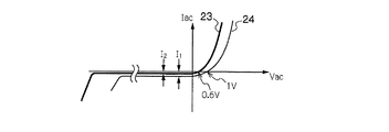
図5は、ショットキーダイオードである窒化物系ダイオード10の電気特性と、図14で説明したような従来のショットキーダイオード(従来例)の電気特性とを示すグラフである。横軸はアノード電極への印加電圧(Vac)を、縦軸はアノード電極からカソード電極へ流れる電流(Iac)をそれぞれ示している。図5では、窒化物系ダイオード10の電気特性を曲線23で、従来例の電気特性を曲線24でそれぞれ示している。図5のグラフで示すように、従来例の場合、逆方向のリーク電流I1が数百μA/mm〜mA/mm程度と非常に大きかったのに対し、本実施形態によれば、逆方向のリーク電流I2を従来例よりも4桁以上下げ、数nA/mm〜数十nA/mm程度にまで下げることが可能になった。また、従来例の場合、オン電圧が1V程度と高かったのに対し、本実施形態によれば、オン電圧を0.6V程度に低減することが出来た。
FIG. 5 is a graph showing the electrical characteristics of the nitride-based
電子供給層14のうち、アノード電極を形成する領域を、チャネル層13に達する深さまで除去して、アノード電極16がメサ18の側面部18aにおいてチャネル層13と直に接触するようにしている。このため、ダイオードの作製が容易になると共に、オン電圧などのバラツキを抑制できる。
A region of the
方向b(図3参照)に長いフィンガー形状のアノード電極16の中心部全体を、同じ方向bに細長い形状を有するメサ18の側面部18aに接触させることで、アノード電極16と2次元電子ガス層17とが線接触し、アノード電極16と2次元電子ガス層17の良好な電気的接続を得ることがきる。
By contacting the entire central portion of the finger-shaped
(第2の実施形態)
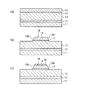
図8は、本発明の第2の実施形態に係る窒化物系ダイオード10Aの概略構成を示している。
この窒化物系ダイオード10Aの特徴は、図1に示す上記第1の実施形態に係る窒化物系ダイオード10において、メサ18の上面全体にSiO2などの絶縁膜30が形成され、メサ18の側面部18aに接触するアノード電極16の一部が絶縁膜30上に延びている構成にある。つまり、アノード電極16が絶縁膜30上からメサ18の側面部18aにわたって形成されている。この窒化物系ダイオード10Aでは、メサ18の側面部18aにおいてチャネル層13と直に接触するアノード電極16が電子供給層14のメサ18の上面に接触する面積を極力低減させた構造になっている。窒化物系ダイオード10Aのその他の構成は、第1の実施形態に係る窒化物系ダイオード10と同様である。
(Second Embodiment)
FIG. 8 shows a schematic configuration of a nitride-based
The nitride-based
このように、窒化物系ダイオード10Aでは、AlGaN/GaN界面に発生する二次元電子ガス層17にアノード電極16が接触して導通が取れている一方で、電子供給層14上(メサ18の上面)にはSiO2などの絶縁膜30(表面保護膜)が形成されており、アノード電極16が電子供給層14に接触する面積を極力低減させた構造になっている。すなわち、電子供給層14表面に絶縁膜30を配し、少なくともアノード電極16との接触は極力チャネル層13だけにすることで、逆方向のリーク電流と耐圧を改善可能な構造にしている。
As described above, in the nitride-based
図8に示す窒化物系ダイオード10Aは以下のようにして作製することが可能である。即ち、成長装置はMOCVD装置を用い、基板は、(111)面を主表面とするシリコン(111)基板11を用いた。
まず、窒化物系ダイオード10の上記作製方法と同様に、図9(a)に示すエピタキシャル層構造を作製する
The
First, the epitaxial layer structure shown in FIG. 9A is manufactured in the same manner as the above-described manufacturing method of the nitride-based
次に、Cl2ガスなどを用いて、チャネル層13および電子供給層14の一部をエッチング除去して素子分離を行う。
次に、電子供給層14のカソード電極およびアノード電極を形成する領域を塩素系ガスを用いてドライエッチングし、チャネル層13に達する深さまで部分的に除去し、メサ18を形成する(図9(b)参照)。
次に、メサ18の上面にSiO2などの絶縁膜30を形成する(図9(c)参照)。
Next, a part of the
Next, the region where the cathode electrode and the anode electrode of the
Next, an insulating
次に、メサ18の側面部18bと接触するように、カソード電極15をリフトオフ法により形成する。
即ち、絶縁膜30を覆うようにチャネル層13の露出した表面および電子供給層14の表面全体にフォトレジスト31を塗布し(図10(a)参照)、このフォトレジスト31を露光、現像して、カソード電極15の形成領域に開口部31aを形成し、さらに、開口部31a内とフォトレジスト31上に金属膜をスパッタ法、真空蒸着法等により形成した後に、フォトレジストを除去することにより残った金属膜をカソード電極15とする(図10(b)参照)。カソード電極15は、例えばTi、Al、Si、Ta、MoあるいはWなどの金属、またはそれらの合金(特にシリサイド合金が好ましい)を含む金属膜である。また、形成したカソード電極15に、オーミック接触を取るための熱処理を施す。
Next, the
That is, a
次に、メサ18の側面部18aと接触するように、アノード電極16をリフトオフ法により形成する。
即ち、カソード電極15および絶縁膜30を覆うようにチャネル層13の露出した表面および電子供給層14の表面全体にフォトレジスト(図示省略)を塗布し、このフォトレジストを露光、現像して、アノード電極16の形成領域に開口部を形成し、さらに、開口部内とフォトレジスト上に金属膜をスパッタ法、真空蒸着法等により形成した後に、フォトレジストを除去することにより残った金属膜をアノード電極16とする(図10(c)参照)。アノード電極は、Ni、Pt、Pd、W、Ta、Alなどの金属或いはこれらの金属の合金を含む金属膜である。
その結果、図8に示した窒化物系ダイオード10Aを作製できた。
Next, the
That is, a photoresist (not shown) is applied to the exposed surface of the
As a result, the
以上の構成を有する第2の実施形態に係る窒化物系ダイオード10Aによれば、上記第1の実施形態が奏する作用効果に加えて以下の作用効果を奏する。電子供給層14の表面状態の不完全性、つまり表面のラフネスが大きいと、メサ18部分の電子供給層14に部分的にトンネル電流が生じる。電子供給層14のメサ18とアノード電極16が接触する面積が大きいと、そのトンネル電流が生じる確率が高くなり、逆方向のリーク電流が増える。そのため、アノード電極16は、電子供給層14のメサ18上面には極力接触させずに、メサ18の側面部18aでチャネル層13に直に接触させるのが好ましい。
第2の実施形態によれば、メサ18の側面部18aにおいてチャネル層13と直に接触するアノード電極16が電子供給層14のメサ18上面に接触する面積を極力低減させた構造になっているので、逆方向のリーク電流が更に低減され、これによって、耐圧が更に向上する。
According to the nitride-based
According to the second embodiment, the area in which the
(第3の実施形態)
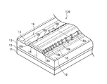
図11は、本発明の第3の実施形態に係る窒化物系ダイオード10Bの主要部を示す斜視図図である。図12は、窒化物系ダイオード10Bを上方から見た図で、図3と同様の模式図である。図13は図11のB−B線に沿った断面図である。この窒化物系ダイオード10Bの特徴は、図1に示す上記第1の実施形態に係る窒化物系ダイオード10Aにおいて、フィンガー形状のカソード電極15およびアノード電極16の各端部に電界が集中しやすいため、電界集中を緩和できるように、以下の構成を採用している点にある。
(Third embodiment)
FIG. 11 is a perspective view showing a main part of a nitride-based
窒化物ダイオード10Bでは、図11乃至図13に示すように、電子供給層14およびチャネル層13は、メサ18がフィンガー部15a、16aの長手な方向(チャネル層13を電流が流れる方向aに対して垂直な方向b)に沿って間欠的に形成されるように部分的に除去されている。
つまり、メサ18の一方の斜面には複数の側面部18aが形成されている(図11参照)。そして、メサ18は、フィンガー形状のアノード電極16とメサ18の各側面部18aとが接触する面積が、フィンガー部16aの先端側(図12で左側)へ向かって徐々に大きくなるように形成されている(図11、図12参照)。
In the
That is, a plurality of
また、メサ18の他方の斜面には複数の側面部18bが形成されている(図11参照)。そして、メサ18は、フィンガー形状のカソード電極15とメサ18の各側面部18bとが接触する面積が、フィンガー部15aの先端側(図12で右側)へ向かって徐々に大きくなるように形成されている(図11、図12参照)。
窒化物系ダイオード10Bのその他の構成は、第2の実施形態に係る窒化物系ダイオード10Aと同様である。
Further, a plurality of
Other configurations of the nitride-based
以上の構成を有する第3の実施形態に係る窒化物系ダイオード10Bによれば、上記第1の実施形態が奏する作用効果に加えて以下の作用効果を奏する。
フィンガー形状のアノード電極16とメサ18の各側面部18aとが接触する面積が、フィンガー部16aの先端側(図12で左側)へ向かって等価的に徐々に大きくなっているので、電界集中しやすいアノード電極16の端部での電界集中が緩和され、電界集中に対して強い構造が実現できる。
According to the nitride-based
The area where the finger-shaped
なお、上記各実施形態では、メサ18の側面部18aにアノード電極16が、その側面部18bにカソード電極15がそれぞれ接触している構成の窒化物系ダイオードについて説明したが、少なくともアノード電極16がメサ18の側面部18aに接触している窒化物系ダイオードに本発明は適用可能である。
In each of the above embodiments, the description has been given of the nitride-based diode in which the
上記各実施形態で説明した窒化物系ダイオードにおいて、2次元電子ガス層17のキャリア濃度を高くし、キャリアの移動度を大きくするために、厚さの薄いAlN層を挿入するのが好ましい。このような構成を有する窒化物系ダイオードでは、上記各実施形態で説明したように、アノード電極16およびカソード電極15をメサ18の側面部18a、18bにそれぞれ接触させることにより、カソード電極15と半導体層(電子供給層14およびチャネル層13)との間で、良好なオーミック接触が得られる。
In the nitride diodes described in the above embodiments, it is preferable to insert a thin AlN layer in order to increase the carrier concentration of the two-dimensional
上記各実施形態では、横型の窒化物系ダイオードについての例を示したが、縦型の窒化物系ダイオードへの適用も可能であることはいうまでも無い。つまり、上記各実施形態において、基板を導電性の基板とし、カソード電極15またはアノード電極16が基板の裏面に形成した裏面電極に電気的に接続されている構成を有する縦型の窒化物系ダイオードにも本発明は適用可能である。
In each of the above embodiments, an example of a lateral nitride-based diode has been described, but it goes without saying that it can also be applied to a vertical nitride-based diode. That is, in each of the above embodiments, a vertical nitride diode having a configuration in which the substrate is a conductive substrate and the
また、上記各実施形態では、一例としてAlGaN/GaNヘテロ接合構造を有する窒化物系ショットキーバリアダイオードとして構成した窒化物系ダイオードについて説明したが、本発明は、ショットキーバリアダイオードに限らず、AlGaN/GaNヘテロ接合構造を有し、アノード電極とカソード電極とを有する窒化物系ダイオードに広く適用可能である。 In each of the above-described embodiments, the nitride-based diode configured as a nitride-based Schottky barrier diode having an AlGaN / GaN heterojunction structure has been described as an example. The present invention is widely applicable to nitride-based diodes having a / GaN heterojunction structure and having an anode electrode and a cathode electrode.
また、上記各実施形態において、チャネル層13をInGaN(第1のGaN系化合物半導体)で構成し、電子供給層14をInAlGaN(第2のGaN系化合物半導体)で構成した窒化物系ダイオードにも本発明は適用可能である。この窒化物系ダイオードでは、InAlGaN/GaNヘテロ接合界面には、自発分極によって、GaN側に高濃度の二次元電子ガス層が形成される。
また、シリコン基板以外のSiC基板、サファイア基板、GaN基板、MgO基板、ZnO基板上など、GaNが結晶成長可能なあらゆる基板上の素子についても成り立つことは言うまでも無い。
In each of the above embodiments, the nitride diode in which the
Further, it goes without saying that elements on all substrates on which GaN can grow crystals, such as SiC substrates other than silicon substrates, sapphire substrates, GaN substrates, MgO substrates, ZnO substrates, and the like are also valid.
10、10A、10B:窒化物系ダイオード
11:シリコン基板 12:バッファ層
13:チャネル層
14:電子供給層
15:カソード電極
15a:フィンガー部
16:アノード電極
16a:フィンガー部
17:2次元電子ガス層
18:メサ
18a、18b:側面部
30:絶縁膜
10, 10A, 10B: Nitride diode 11: Silicon substrate 12: Buffer layer 13: Channel layer 14: Electron supply layer 15:
Claims (9)
前記チャネル層上に形成され、第2の窒化物系化合物半導体からなる電子供給層と、
前記電子供給層上に形成されたカソード電極およびアノード電極と、
前記電子供給層の一部を、前記チャネル層に達する深さまで部分的に除去したメサと、を備え、
前記メサの側面部に、前記カソード電極およびアノード電極のうち、少なくとも前記アノード電極が接触していることを特徴とする窒化物系ダイオード。 A channel layer made of a first nitride-based compound semiconductor formed on a substrate;
An electron supply layer formed on the channel layer and made of a second nitride compound semiconductor;
A cathode electrode and an anode electrode formed on the electron supply layer;
A mesa partially removed to a depth reaching the channel layer, a part of the electron supply layer,
A nitride-based diode, wherein at least the anode electrode of the cathode electrode and the anode electrode is in contact with a side surface portion of the mesa.
前記メサが前記フィンガー部の長手方向に沿って間欠的に形成されていることを特徴とする請求項1又は2に記載の窒化物系ダイオード。 The cathode electrode and the anode electrode have finger portions,
The nitride diode according to claim 1 or 2, wherein the mesa is intermittently formed along a longitudinal direction of the finger portion.
Priority Applications (1)
| Application Number | Priority Date | Filing Date | Title |
|---|---|---|---|
| JP2009278331A JP5675084B2 (en) | 2009-12-08 | 2009-12-08 | Nitride diode |
Applications Claiming Priority (1)
| Application Number | Priority Date | Filing Date | Title |
|---|---|---|---|
| JP2009278331A JP5675084B2 (en) | 2009-12-08 | 2009-12-08 | Nitride diode |
Publications (2)
| Publication Number | Publication Date |
|---|---|
| JP2011124258A true JP2011124258A (en) | 2011-06-23 |
| JP5675084B2 JP5675084B2 (en) | 2015-02-25 |
Family
ID=44287894
Family Applications (1)
| Application Number | Title | Priority Date | Filing Date |
|---|---|---|---|
| JP2009278331A Active JP5675084B2 (en) | 2009-12-08 | 2009-12-08 | Nitride diode |
Country Status (1)
| Country | Link |
|---|---|
| JP (1) | JP5675084B2 (en) |
Cited By (17)
| Publication number | Priority date | Publication date | Assignee | Title |
|---|---|---|---|---|
| WO2013008414A1 (en) * | 2011-07-08 | 2013-01-17 | パナソニック株式会社 | Rectifier device |
| JPWO2013005372A1 (en) * | 2011-07-01 | 2015-02-23 | パナソニック株式会社 | Semiconductor device |
| WO2015077916A1 (en) * | 2013-11-26 | 2015-06-04 | 中国科学院半导体研究所 | Gan-based schottky barrier diode rectifier |
| KR20150084855A (en) * | 2012-11-16 | 2015-07-22 | 비샤이 제너럴 세미컨덕터 엘엘씨 | GaN-BASED SCHOTTKY DIODE HAVING DUAL METAL, PARTIALLY RECESSED ELECTRODE |
| JP2016501443A (en) * | 2012-11-16 | 2016-01-18 | ヴィシャイ ジェネラル セミコンダクター エルエルシーVishay General Semiconductor LLC | GaN-based Schottky diode with partially recessed anode |
| WO2018003855A1 (en) | 2016-06-28 | 2018-01-04 | 株式会社スリーボンド | Curable resin composition, fuel cell, and sealing method |
| WO2018047479A1 (en) | 2016-09-06 | 2018-03-15 | 株式会社スリーボンド | Curable resin composition, fuel cell using same and sealing method using same |
| KR20180035227A (en) | 2015-07-30 | 2018-04-05 | 가부시끼가이샤 쓰리본드 | Photocurable resin composition, fuel cell and sealing method |
| KR20180037972A (en) | 2015-07-30 | 2018-04-13 | 가부시끼가이샤 쓰리본드 | Photocurable resin composition, fuel cell and sealing method |
| KR20180041680A (en) | 2015-08-18 | 2018-04-24 | 가부시끼가이샤 쓰리본드 | Photo-curable sealant for fuel cell, fuel cell and sealing method |
| KR20180050317A (en) | 2015-09-02 | 2018-05-14 | 가부시끼가이샤 쓰리본드 | Photocurable resin composition, fuel cell and sealing method |
| WO2018190421A1 (en) | 2017-04-14 | 2018-10-18 | 株式会社スリーボンド | Photocurable resin composition, fuel cell using same, and sealing method |
| WO2018190417A1 (en) | 2017-04-14 | 2018-10-18 | 株式会社スリーボンド | Curable resin composition, fuel cell using same, and sealing method |
| WO2018190415A1 (en) | 2017-04-14 | 2018-10-18 | 株式会社スリーボンド | Photocurable resin composition, fuel cell using same, and sealing method |
| KR20180120159A (en) | 2016-03-09 | 2018-11-05 | 가부시끼가이샤 쓰리본드 | Curable resin composition, fuel cell and sealing method |
| KR20190031477A (en) | 2016-07-14 | 2019-03-26 | 가부시끼가이샤 쓰리본드 | Curable resin composition, cured product, fuel cell and sealing method |
| WO2019124252A1 (en) | 2017-12-18 | 2019-06-27 | 株式会社スリーボンド | Curable resin composition, and fuel cell and sealing method using same |
Citations (5)
| Publication number | Priority date | Publication date | Assignee | Title |
|---|---|---|---|---|
| WO2006038390A1 (en) * | 2004-09-30 | 2006-04-13 | Sanken Electric Co., Ltd. | Semiconductor device |
| JP2006108676A (en) * | 2004-09-30 | 2006-04-20 | Internatl Rectifier Corp | Group iii nitride multichannel hetero-junction interdigital rectifier |
| JP2006156457A (en) * | 2004-11-25 | 2006-06-15 | Matsushita Electric Ind Co Ltd | Schottky barrier diode and diode array |
| JP2009117485A (en) * | 2007-11-02 | 2009-05-28 | Panasonic Corp | Nitride semiconductor device |
| JP2009124001A (en) * | 2007-11-16 | 2009-06-04 | Furukawa Electric Co Ltd:The | Gan-based semiconductor device |
-
2009
- 2009-12-08 JP JP2009278331A patent/JP5675084B2/en active Active
Patent Citations (5)
| Publication number | Priority date | Publication date | Assignee | Title |
|---|---|---|---|---|
| WO2006038390A1 (en) * | 2004-09-30 | 2006-04-13 | Sanken Electric Co., Ltd. | Semiconductor device |
| JP2006108676A (en) * | 2004-09-30 | 2006-04-20 | Internatl Rectifier Corp | Group iii nitride multichannel hetero-junction interdigital rectifier |
| JP2006156457A (en) * | 2004-11-25 | 2006-06-15 | Matsushita Electric Ind Co Ltd | Schottky barrier diode and diode array |
| JP2009117485A (en) * | 2007-11-02 | 2009-05-28 | Panasonic Corp | Nitride semiconductor device |
| JP2009124001A (en) * | 2007-11-16 | 2009-06-04 | Furukawa Electric Co Ltd:The | Gan-based semiconductor device |
Cited By (31)
| Publication number | Priority date | Publication date | Assignee | Title |
|---|---|---|---|---|
| JPWO2013005372A1 (en) * | 2011-07-01 | 2015-02-23 | パナソニック株式会社 | Semiconductor device |
| WO2013008414A1 (en) * | 2011-07-08 | 2013-01-17 | パナソニック株式会社 | Rectifier device |
| KR102011761B1 (en) * | 2012-11-16 | 2019-08-19 | 비샤이 제너럴 세미컨덕터 엘엘씨 | GaN-BASED SCHOTTKY DIODE HAVING DUAL METAL, PARTIALLY RECESSED ELECTRODE |
| KR20150084855A (en) * | 2012-11-16 | 2015-07-22 | 비샤이 제너럴 세미컨덕터 엘엘씨 | GaN-BASED SCHOTTKY DIODE HAVING DUAL METAL, PARTIALLY RECESSED ELECTRODE |
| JP2016501442A (en) * | 2012-11-16 | 2016-01-18 | ヴィシャイ ジェネラル セミコンダクター エルエルシーVishay General Semiconductor LLC | GaN-based Schottky diode with dual metal, partially recessed electrode |
| JP2016501443A (en) * | 2012-11-16 | 2016-01-18 | ヴィシャイ ジェネラル セミコンダクター エルエルシーVishay General Semiconductor LLC | GaN-based Schottky diode with partially recessed anode |
| WO2015077916A1 (en) * | 2013-11-26 | 2015-06-04 | 中国科学院半导体研究所 | Gan-based schottky barrier diode rectifier |
| KR20180035227A (en) | 2015-07-30 | 2018-04-05 | 가부시끼가이샤 쓰리본드 | Photocurable resin composition, fuel cell and sealing method |
| US10840517B2 (en) | 2015-07-30 | 2020-11-17 | Threebond Co., Ltd. | Photocurable resin composition, fuel cell, and sealing method |
| KR20180037972A (en) | 2015-07-30 | 2018-04-13 | 가부시끼가이샤 쓰리본드 | Photocurable resin composition, fuel cell and sealing method |
| US10840518B2 (en) | 2015-07-30 | 2020-11-17 | Threebond Co., Ltd. | Photocurable resin composition, fuel cell, and sealing method |
| KR20180041680A (en) | 2015-08-18 | 2018-04-24 | 가부시끼가이샤 쓰리본드 | Photo-curable sealant for fuel cell, fuel cell and sealing method |
| KR20180050317A (en) | 2015-09-02 | 2018-05-14 | 가부시끼가이샤 쓰리본드 | Photocurable resin composition, fuel cell and sealing method |
| US11261301B2 (en) | 2015-09-02 | 2022-03-01 | Threebond Co., Ltd. | Photocurable resin composition, fuel cell, and sealing method |
| US10800952B2 (en) | 2016-03-09 | 2020-10-13 | Threebond Co., Ltd. | Curable resin composition, fuel cell, and sealing method |
| KR20180120159A (en) | 2016-03-09 | 2018-11-05 | 가부시끼가이샤 쓰리본드 | Curable resin composition, fuel cell and sealing method |
| WO2018003855A1 (en) | 2016-06-28 | 2018-01-04 | 株式会社スリーボンド | Curable resin composition, fuel cell, and sealing method |
| US10907037B2 (en) | 2016-06-28 | 2021-02-02 | Threebond Co., Ltd. | Curable resin composition, fuel cell, and sealing method |
| KR20190022511A (en) | 2016-06-28 | 2019-03-06 | 가부시끼가이샤 쓰리본드 | Curable resin composition, fuel cell and sealing method |
| KR20190031477A (en) | 2016-07-14 | 2019-03-26 | 가부시끼가이샤 쓰리본드 | Curable resin composition, cured product, fuel cell and sealing method |
| US10865297B2 (en) | 2016-07-14 | 2020-12-15 | Threebond Co., Ltd. | Curable resin composition, cured product, fuel cell, and sealing method |
| KR20190050966A (en) | 2016-09-06 | 2019-05-14 | 가부시끼가이샤 쓰리본드 | Curable resin composition, fuel cell and sealing method using the same |
| US11165072B2 (en) | 2016-09-06 | 2021-11-02 | Threebond Co., Ltd. | Curable resin composition, fuel cell using same, and sealing method using same |
| WO2018047479A1 (en) | 2016-09-06 | 2018-03-15 | 株式会社スリーボンド | Curable resin composition, fuel cell using same and sealing method using same |
| WO2018190415A1 (en) | 2017-04-14 | 2018-10-18 | 株式会社スリーボンド | Photocurable resin composition, fuel cell using same, and sealing method |
| US11114679B2 (en) | 2017-04-14 | 2021-09-07 | Threebond Co., Ltd. | Curable resin composition, and fuel cell and sealing method using the same |
| WO2018190417A1 (en) | 2017-04-14 | 2018-10-18 | 株式会社スリーボンド | Curable resin composition, fuel cell using same, and sealing method |
| WO2018190421A1 (en) | 2017-04-14 | 2018-10-18 | 株式会社スリーボンド | Photocurable resin composition, fuel cell using same, and sealing method |
| US11414512B2 (en) | 2017-04-14 | 2022-08-16 | Threebond Co., Ltd. | Photocurable resin composition, fuel cell using same, and sealing method |
| KR20200090918A (en) | 2017-12-18 | 2020-07-29 | 가부시끼가이샤 쓰리본드 | Curable resin composition, fuel cell and sealing method using same |
| WO2019124252A1 (en) | 2017-12-18 | 2019-06-27 | 株式会社スリーボンド | Curable resin composition, and fuel cell and sealing method using same |
Also Published As
| Publication number | Publication date |
|---|---|
| JP5675084B2 (en) | 2015-02-25 |
Similar Documents
| Publication | Publication Date | Title |
|---|---|---|
| JP5675084B2 (en) | Nitride diode | |
| JP4691060B2 (en) | GaN-based semiconductor devices | |
| TWI431770B (en) | Semiconductor device and method for manufacturing the same | |
| JP5114947B2 (en) | Nitride semiconductor device and manufacturing method thereof | |
| JP5566670B2 (en) | GaN-based field effect transistor | |
| JP5841417B2 (en) | Nitride semiconductor diode | |
| JP5367429B2 (en) | GaN-based field effect transistor | |
| JP5655424B2 (en) | Compound semiconductor device | |
| JP2012104567A (en) | Semiconductor device and method of manufacturing the same | |
| WO2013137267A1 (en) | Nitride compound semiconductor element | |
| KR20150084855A (en) | GaN-BASED SCHOTTKY DIODE HAVING DUAL METAL, PARTIALLY RECESSED ELECTRODE | |
| WO2013161478A1 (en) | Nitride semiconductor element | |
| JP6343807B2 (en) | Field effect transistor and manufacturing method thereof | |
| JP4875660B2 (en) | III-V nitride semiconductor device | |
| JP5055773B2 (en) | Semiconductor element | |
| JP2006286698A (en) | Electronic device and power converter | |
| JP5355927B2 (en) | Semiconductor device and manufacturing method of semiconductor device | |
| JP5379391B2 (en) | Semiconductor device comprising gallium nitride compound semiconductor and method for manufacturing the same | |
| JP5605353B2 (en) | MIS type semiconductor device and manufacturing method thereof | |
| JP2009124001A (en) | Gan-based semiconductor device | |
| JP2012064663A (en) | Nitride semiconductor device and method of manufacturing the same | |
| JP2008022029A (en) | GaN-BASED SEMICONDUCTOR DEVICE AND GROUP III-V NITRIDE SEMICONDUCTOR DEVICE | |
| JP2007088186A (en) | Semiconductor device and its fabrication process | |
| JP2009060065A (en) | Nitride semiconductor device | |
| JP2010010412A (en) | Semiconductor element, and manufacturing method thereof |
Legal Events
| Date | Code | Title | Description |
|---|---|---|---|
| A621 | Written request for application examination |
Free format text: JAPANESE INTERMEDIATE CODE: A621 Effective date: 20120801 |
|
| A977 | Report on retrieval |
Free format text: JAPANESE INTERMEDIATE CODE: A971007 Effective date: 20140122 |
|
| A131 | Notification of reasons for refusal |
Free format text: JAPANESE INTERMEDIATE CODE: A131 Effective date: 20140131 |
|
| A977 | Report on retrieval |
Free format text: JAPANESE INTERMEDIATE CODE: A971007 Effective date: 20140313 |
|
| A521 | Written amendment |
Free format text: JAPANESE INTERMEDIATE CODE: A523 Effective date: 20140401 |
|
| TRDD | Decision of grant or rejection written | ||
| A01 | Written decision to grant a patent or to grant a registration (utility model) |
Free format text: JAPANESE INTERMEDIATE CODE: A01 Effective date: 20141205 |
|
| A61 | First payment of annual fees (during grant procedure) |
Free format text: JAPANESE INTERMEDIATE CODE: A61 Effective date: 20141224 |
|
| R151 | Written notification of patent or utility model registration |
Ref document number: 5675084 Country of ref document: JP Free format text: JAPANESE INTERMEDIATE CODE: R151 |
|
| S531 | Written request for registration of change of domicile |
Free format text: JAPANESE INTERMEDIATE CODE: R313531 |
|
| R350 | Written notification of registration of transfer |
Free format text: JAPANESE INTERMEDIATE CODE: R350 |