JP2011106983A - Semiconductor integrated circuit and test circuit insertion method - Google Patents
Semiconductor integrated circuit and test circuit insertion method Download PDFInfo
- Publication number
- JP2011106983A JP2011106983A JP2009262770A JP2009262770A JP2011106983A JP 2011106983 A JP2011106983 A JP 2011106983A JP 2009262770 A JP2009262770 A JP 2009262770A JP 2009262770 A JP2009262770 A JP 2009262770A JP 2011106983 A JP2011106983 A JP 2011106983A
- Authority
- JP
- Japan
- Prior art keywords
- circuit
- path
- delay
- test
- signal
- Prior art date
- Legal status (The legal status is an assumption and is not a legal conclusion. Google has not performed a legal analysis and makes no representation as to the accuracy of the status listed.)
- Withdrawn
Links
Images


Landscapes
- Tests Of Electronic Circuits (AREA)
- Semiconductor Integrated Circuits (AREA)
Abstract
【課題】複数の所定のレジスタ間のタイミングを変えることなく、テスト回路を挿入する。
【解決手段】半導体集積回路は、部分経路(111〜114)を形成する回路ブロックと、遅延回路(121〜124)と、選択回路(131〜134)と、制御回路(140)とを具備する。部分経路(111〜114)を形成する回路ブロックは、第1フリップフロップ(101)から出力される信号が第2フリップフロップ(102)に入力するまでの信号経路に含まれる。遅延回路(121〜124)は、部分経路を信号が伝播するときの遅延特性に等価な遅延特性を有して部分経路(111〜114)を模擬する。選択回路(131〜134)は、部分経路(111〜114)の出力信号と、遅延回路(121〜124)の出力信号とのうちの一方を選択して出力する。制御回路(140)は、経路遅延故障を検出する経路遅延故障テストのときに、選択回路(131〜134)が選択する信号を制御する。
【選択図】図2A test circuit is inserted without changing the timing between a plurality of predetermined registers.
A semiconductor integrated circuit includes a circuit block forming partial paths (111 to 114), a delay circuit (121 to 124), a selection circuit (131 to 134), and a control circuit (140). . The circuit blocks forming the partial paths (111 to 114) are included in the signal path until the signal output from the first flip-flop (101) is input to the second flip-flop (102). The delay circuit (121 to 124) has a delay characteristic equivalent to the delay characteristic when a signal propagates through the partial path, and simulates the partial path (111 to 114). The selection circuits (131 to 134) select and output one of the output signals of the partial paths (111 to 114) and the output signals of the delay circuits (121 to 124). The control circuit (140) controls a signal selected by the selection circuits (131 to 134) during a path delay fault test for detecting a path delay fault.
[Selection] Figure 2
Description
本発明は、半導体集積回路および試験方法に関し、特に半導体集積回路の遅延故障テストおよびテスト回路の挿入方法に関する。 The present invention relates to a semiconductor integrated circuit and a test method, and more particularly to a delay fault test of a semiconductor integrated circuit and a test circuit insertion method.
近年、LSIの高集積化および高速化によりタイミング遅延故障によるLSI不良が増加しており、スキャンテスト手法を用いた遅延故障テストの重要性が高まっている。 In recent years, LSI failures due to timing delay faults have increased due to higher integration and higher speed of LSIs, and the importance of delay fault tests using scan test techniques has increased.
従来は遅延故障テストで一般的に用いられる遷移遅延故障テストとして、順序回路間に存在する複数パスのうち1つのパスについてテストパターンが遷移させることが出来れば、遅延故障が検出されたと定義していた。 Conventionally, as a transition delay fault test generally used in a delay fault test, it is defined that a delay fault has been detected if the test pattern can be transitioned for one path among multiple paths existing between sequential circuits. It was.
複数パスが含まれる回路において、論理段数が多いパスと少ないパスが含まれている場合に、テストパターンを生成するATPG(Automatic Test Pattern Generator)は、論理段数が少なく検出しやすい側のパスで検出したと見なす事が多く、従来の遅延故障テストは、精度の低い方法が一般的であった。 In a circuit including multiple paths, when a path with a large number of logic stages and a path with a small number of logic stages are included, an ATPG (Automatic Test Pattern Generator) that generates a test pattern is detected with a path on the side where the number of logic stages is small and easy to detect. In many cases, conventional delay fault testing is generally performed with low accuracy.
しかし、遅延故障テストとしては、論理段数の多い側のパスも含めてすべてのパスを検出する方が望ましく、近年では故障検出率を向上させることにより、製品の品質を向上させることが重要視されてきた。その中で回路内のクリティカルパス等の論理段数の多い特定パスを、遅延故障テストのなかで検出可能とすることの必要性が高まってきた。 However, as a delay fault test, it is desirable to detect all paths including paths on the side with a large number of logical stages. In recent years, it has been emphasized to improve product quality by improving the fault detection rate. I came. There is a growing need to be able to detect a specific path having a large number of logical stages such as a critical path in a circuit in a delay fault test.
図1に、特開2001−13220号公報に記載のテスト回路が示される。このテスト回路を備える半導体集積回路は、設計上(実用上)100MHz(周期10n秒)のクロックによって動作する性能を有する。検査回路300は、信号伝播経路の検査の対象となる論理回路320と、検査信号発生点として論理回路320に入力される検査信号を生成するレジスタ301と、検査信号観測点として論理回路320から出力される検査信号を観測するためのレジスタ302及び303と、検査信号発生点及び検査信号観測点に動作タイミング(検査信号の発生タイミング及び検査信号の観測タイミング)を設定する検査タイミング生成部310とを有する。
FIG. 1 shows a test circuit described in Japanese Patent Application Laid-Open No. 2001-13220. A semiconductor integrated circuit including this test circuit has a performance that operates by a clock of 100 MHz (
また、論理回路320は、検査信号の再収斂点を構成する論理素子329と、論理素子329と検査信号発生点であるレジスタ301との間に位置する部分経路324、325と、論理素子329と検査信号観測点であるレジスタ302との間に位置する部分経路326、327と、論理素子209と検査信号観測点であるレジスタ303との間に位置する部分経路328とを有する。
The
この検査回路100において、信号伝播経路は、検査信号発生点であるレジスタ201から2つの部分経路204、205に分岐し、再収斂点である論理素子329で再収斂している。さらに、信号伝播経路は、再収斂点である論理素子329から3つの部分経路326、327、328に分岐する。部分経路326、327は、検査信号観測点であるレジスタ302の直前で再度再収斂し、部分経路208は検査信号観測点であるレジスタ303に達する。ここでは、上記部分経路324、325、326、327、328を信号が伝播するのに要する時間、すなわち各部分経路の設計上の遅延時間は、それぞれ4n秒、2n秒、4n秒、2n秒、4n秒となっている。
In this test circuit 100, the signal propagation path branches from the
検査回路300には、さらに、起点側付加レジスタ361と、終点側付加レジスタ362と、遅延素子部363と、遅延素子部364とが付加されている。起点側付加レジスタ361は、検査信号発生点として論理回路320に検査信号を与える。遅延素子部363は、起点側付加レジスタ361と論理素子329との間に配置され、検査信号発生点となる起点側付加レジスタ361からの検査信号を所定時間だけ遅延させた検査信号を再収斂点である論理素子329に出力する。遅延素子部364は、論理素子329と終点側付加レジスタ362との間に配置され、再収斂点である論理素子329から出力される検査信号を所定時間だけ遅延する。終点側付加レジスタ362は、検査信号観測点として論理回路320から出力される検査信号を観測するためのレジスタである。
The
遅延素子部363は、1つの遅延素子Daを含む遅延回路363aと、直列接続される2つの遅延素子Db1、Db2を含む遅延回路363bと、選択回路363cとを備える。遅延回路363aは、検査信号発生点であるレジスタ361からの検査信号を所定時間(6n秒)遅延する。遅延回路363bは、検査信号発生点であるレジスタ361からの検査信号を所定時間(7n秒)遅延する。選択回路363cは、両遅延回路363a及び363bの出力の一方を、外部のテスタなどからの遅延時間選択信号SELAに基づいて選択して出力する。
The
遅延素子部364は、1つの遅延素子Dcを含む遅延回路364aと、直列接続される2つの遅延素子Dd1、Dd2を含む遅延回路364bと、選択回路364cとを備える。遅延回路364aは、再収斂点としての論理素子329からの検査信号を所定時間(5n秒)遅延する。遅延回路364bは、再収斂点としての論理素子329からの検査信号を所定時間(8n秒)遅延する。選択回路364cは、各遅延回路364a及び364bの出力の一方を、外部のテスタなどからの遅延時間選択信号SELBに基づいて選択して出力する。
The
この検査回路300は、第2の検査信号発生点であるレジスタ361および第2の検査信号観測点であるレジスタ362を備えているので、検査回路には、11個の信号伝播経路が形成されることとなる。
Since the
第1の信号伝播経路は、部分経路324、論理素子329、及び部分経路326を含む。第2の信号伝播経路は、部分経路324、論理素子329、及び部分経路327を含む。第3の信号伝播経路は、部分経路325、論理素子329、及び部分経路326を含む。また、第4の信号伝播経路は、部分経路325、論理素子329、及び部分経路327を含む。第5の信号伝播経路は、部分経路324、論理素子329、及び部分経路328を含む。第6の信号伝播経路は、部分経路325、論理素子329、及び部分経路328を含む。さらに、第7の信号伝播経路は、部分経路324、論理素子329、及び遅延回路364を含む。第8の信号伝播経路は、部分経路325、論理素子329、及び遅延回路364を含む。第9の信号伝播経路は、遅延回路363、論理素子329、及び部分経路326を含む。また、第10の信号伝播経路は、遅延回路363、論理素子329、及び部分経路327を含む。第11の信号伝播経路は、遅延回路363、論理素子329、及び部分経路328を含む。但し、ここでは、第7、第8、第9、第10、第11の信号伝播経路は、半導体集積回路の機能上不要であるために、遅延故障無しの保証は必ずしも必要ではない。
The first signal propagation path includes a
このテスト回路は、遅延回路363、および遅延回路364の伝播経路を設定するために、検査信号発生点であるレジスタ361および検査信号観測点であるレジスタ362を、テストに用いる順序回路として追加している。そのため、クリティカルパスに対して、テスト回路の挿入を行うことが困難である。
In order to set the propagation path of the
一般的には、タイミングの厳しいパス、すなわちクリティカルパスは、確実な動作が要求されるため、レイアウト設計を行ったのちにテストパターンによる確認が必須であり、経路遅延故障テストの対象とされる。この経路遅延故障テストのパスが、テストパターンでの確認が困難な場合に、上記のようなテスト回路が用いられる。 Generally, a path with strict timing, that is, a critical path is required to have a reliable operation. Therefore, after a layout design, confirmation by a test pattern is indispensable, and a path delay fault test is performed. When the path delay fault test path is difficult to confirm with a test pattern, the above test circuit is used.
しかし、追加されるテスト回路は、順序回路を含んでいる。順序回路は、検査タイミング生成部で内部回路の動作クロックと同じクロックで動作することから、新たなクロック配線が追加される。そのため、クロック配線の再構築が必要となる。 However, the added test circuit includes a sequential circuit. Since the sequential circuit operates with the same clock as the operation clock of the internal circuit in the inspection timing generation unit, a new clock wiring is added. Therefore, it is necessary to reconstruct the clock wiring.
クロック配線の再構築により、クロック遅延値が変動すると、タイミングの厳しいパスと判断していたパスがクリティカルパスでは無くなり、新たにタイミングの厳しいパスが生じる場合がある。 When the clock delay value fluctuates due to the reconstruction of the clock wiring, the path determined to be a path with strict timing is not a critical path, and a path with strict timing may be newly generated.
順序回路の挿入を必要とするこのようなテスト回路では、テスト回路自身の挿入によりタイミングの厳しいパスが変動する可能性がある。したがって、タイミングの厳しいパスが変更された場合は、再度テスト回路の挿入が必要になる。すなわち、このような方法では、クリティカルパスに対するテスト回路が一度の処理で挿入を完結出来ない、つまりテスト回路の挿入が困難である。 In such a test circuit that requires the insertion of a sequential circuit, there is a possibility that a path with severe timing may change due to the insertion of the test circuit itself. Therefore, when a path with strict timing is changed, it is necessary to insert a test circuit again. That is, in such a method, the test circuit for the critical path cannot be completely inserted by one process, that is, it is difficult to insert the test circuit.
本発明は、複数の所定のレジスタ間のタイミングを変えることなく、テスト回路が挿入される半導体集積回路およびテスト回路挿入方法を提供する。 The present invention provides a semiconductor integrated circuit and a test circuit insertion method in which a test circuit is inserted without changing the timing between a plurality of predetermined registers.
以下に、[発明を実施するための形態]で使用される番号・符号を用いて、課題を解決するための手段を説明する。これらの番号・符号は、[特許請求の範囲]の記載と[発明を実施するための形態]との対応関係を明らかにするために付加されたものである。ただし、それらの番号・符号を、[特許請求の範囲]に記載されている発明の技術的範囲の解釈に用いてはならない。 Hereinafter, means for solving the problem will be described using the numbers and symbols used in the “DETAILED DESCRIPTION”. These numbers and symbols are added to clarify the correspondence between the description of [Claims] and [Mode for Carrying Out the Invention]. However, these numbers and symbols should not be used for the interpretation of the technical scope of the invention described in [Claims].
本発明の観点では、半導体集積回路は、部分経路(111〜114)を形成する回路ブロックと、遅延回路(121〜124)と、選択回路(131〜134)と、制御回路(140)とを具備する。部分経路(111〜114)を形成する回路ブロックは、第1フリップフロップ(101)から出力される信号が第2フリップフロップ(102)に入力するまでの信号経路に含まれる。遅延回路(121〜124)は、部分経路を信号が伝播するときの遅延特性に等価な遅延特性を有して部分経路(111〜114)を模擬する。選択回路(131〜134)は、部分経路(111〜114)の出力信号と、遅延回路(121〜124)の出力信号とのうちの一方を選択して出力する。制御回路(140)は、経路遅延故障を検出する経路遅延故障テストのときに、選択回路(131〜134)が選択する信号を制御する。 In an aspect of the present invention, a semiconductor integrated circuit includes a circuit block that forms partial paths (111 to 114), a delay circuit (121 to 124), a selection circuit (131 to 134), and a control circuit (140). It has. The circuit blocks forming the partial paths (111 to 114) are included in the signal path until the signal output from the first flip-flop (101) is input to the second flip-flop (102). The delay circuit (121 to 124) has a delay characteristic equivalent to the delay characteristic when a signal propagates through the partial path, and simulates the partial path (111 to 114). The selection circuits (131 to 134) select and output one of the output signals of the partial paths (111 to 114) and the output signals of the delay circuits (121 to 124). The control circuit (140) controls a signal selected by the selection circuits (131 to 134) during a path delay fault test for detecting a path delay fault.
本発明の他の観点では、テスト回路挿入方法は、半導体集積回路の遅延故障を試験するときのテスト回路を挿入する方法であり、クリティカルパスを抽出するステップと、未検出リストを生成するステップと、非活性リストを生成するステップと、テスト回路を挿入するステップとを具備する。クリティカルパスを抽出するステップでは、所定の時間内に第1フリップフロップから第2フリップフロップまで信号を伝播する必要のあるクリティカルパスが抽出される。未検出リストを生成するステップでは、入力データに応答して出力側の信号が変化するテストパターンが生成できないクリティカルパス内の未検出ネットが抽出され、未検出リストが生成される。非活性リストを生成するステップでは、故障シミュレーションを実行して検出されるクリティカルパス内で信号が変化しないネットを示す非活性ネットが抽出され、非活性リストが生成される。テスト回路を挿入するステップでは、未検出リストと非活性リストとに基づいて、未検出ネットまたは非活性ネットを含む信号伝播経路に遅延回路および選択回路を備えるテスト回路が挿入される。 In another aspect of the present invention, a test circuit insertion method is a method of inserting a test circuit when testing a delay fault in a semiconductor integrated circuit, and includes a step of extracting a critical path and a step of generating an undetected list. Generating a deactivation list and inserting a test circuit. In the step of extracting a critical path, a critical path that needs to propagate a signal from the first flip-flop to the second flip-flop within a predetermined time is extracted. In the step of generating an undetected list, an undetected net in a critical path where a test pattern in which a signal on the output side changes in response to input data cannot be generated is extracted, and an undetected list is generated. In the step of generating an inactive list, an inactive net indicating a net whose signal does not change in a critical path detected by executing a failure simulation is extracted, and an inactive list is generated. In the step of inserting a test circuit, a test circuit including a delay circuit and a selection circuit is inserted into a signal propagation path including an undetected net or an inactive net based on the undetected list and the inactive list.
本発明によれば、複数の所定のレジスタ間のタイミングを変えることのないテスト回路が挿入される半導体集積回路およびその半導体集積回路にテスト回路を挿入するテスト回路挿入方法を提供することができる。 According to the present invention, it is possible to provide a semiconductor integrated circuit into which a test circuit that does not change the timing between a plurality of predetermined registers is inserted, and a test circuit insertion method for inserting a test circuit into the semiconductor integrated circuit.
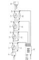
図2に、第1の実施の形態に係るテスト回路の回路ブロック図が示される。 FIG. 2 shows a circuit block diagram of the test circuit according to the first embodiment.
半導体集積回路は、経路遅延故障テストの始点であるDフリップフロップ101、終点であるDフリップフロップ102の順序回路間に、部分経路111、112、113、114を備える。Dフリップフロップ101の出力と選択回路131の入力との間に部分経路111と遅延素子121とが並列に接続される。遅延素子121の遅延特性は、部分経路111と等価である。
The semiconductor integrated circuit includes
選択回路131の出力と選択回路132の入力との間に部分経路112と遅延素子122とが並列に接続される。遅延素子122の遅延特性は、部分経路112と等価である。選択回路132の出力と選択回路133の入力との間に部分経路113と遅延素子123とが並列に接続される。遅延素子123の遅延特性は、部分経路113と等価である。選択回路133の出力と選択回路134の入力との間に部分経路114と遅延素子124とが並列に接続される。遅延素子124の遅延特性は、部分経路114と等価である。選択回路134の出力は、終点のDフリップフロップ102のD入力に接続される。
The
観測領域制御回路140は、選択回路131、132、133、134の出力を選択する制御信号DSEL1、DSEL2、DSEL3、DSEL4を出力する。観測領域制御回路140には、経路遅延故障テストの動作開始を示す信号TESTと、テスト動作モードを指示する信号TDEC0、TDEC1とが入力される。観測領域制御回路140は、信号TDEC0、TDEC1をデコードして、選択回路131〜134の選択を切り換える制御信号DSEL1〜DSEL4を生成する。図3に、入力信号と出力信号との関係を示す真理値表が示される。
The observation
図2、図3を参照して、第1の実施の形態に係るテスト回路の動作を説明する。 The operation of the test circuit according to the first embodiment will be described with reference to FIGS.
観測領域制御回路140は、信号TESTが“1”(アクティブ)になるとテストモードの動作を開始する。観測領域制御回路140は、信号TDEC0および信号TDEC1に基づいて、テストされる部分経路111、112、113、114のいずれかを選択するように、信号DSEL1〜DSEL4を選択回路131〜134に供給する。
The observation
部分経路111の経路遅延故障テストを行う場合、テストモード1として、信号TDEC0、信号TDEC1には共に“0”が設定される。このとき、図3のテストモード1に示されるように、観測領域制御回路140は、信号DSEL1に“0”、信号DSEL2〜4に“1”を出力する。したがって、選択回路131が部分経路111の出力を選択し、他の選択回路132〜134は、遅延素子122〜124の出力を選択するように設定される。経路遅延故障テストの経路は、Dフリップフロップ101のQ出力から部分経路111、遅延素子122、遅延素子123、遅延素子124を経由してDフリップフロップ102のD入力に至る経路となる。このように経路遅延故障テストの経路が設定された後、経路遅延故障テストのためのテストパターンが実行される。Dフリップフロップ102のD入力には、部分経路111と遅延素子122〜124とを経由した信号が到達する。したがって、テストモード1では部分経路111のみを対象としたテストが容易に実施できる。
When the path delay fault test of the
部分経路112の経路遅延故障テストを行う場合、テストモード2として信号TDEC0に“0”、信号TDEC1に“1”が設定される。このとき、図3のテストモード2に示されるように、観測領域制御回路140は、信号DSEL2に“0”、信号DSEL1、DSEL3、DSEL4に“1”を出力する。したがって、選択回路132が部分経路112の出力を選択し、他の選択回路131、133、134は、遅延素子121、123、124の出力を選択するように設定される。経路遅延故障テストの経路は、Dフリップフロップ101のQ出力から遅延素子121、部分経路112、遅延素子123、遅延素子124を経由してDフリップフロップ102のD入力に至る経路となる。このように経路遅延故障テストの経路が設定された後、経路遅延故障テストのためのテストパターンが実行される。Dフリップフロップ102のD入力には、遅延素子121、部分経路112、遅延素子123、124を経由した信号が到達する。したがって、テストモード2では部分経路112のみを対象としたテストが容易に実施できる。
When the path delay fault test of the
部分経路113の経路遅延故障テストを行う場合、テストモード3として、信号TDEC0に“1”、信号TDEC1に“0”が設定される。このとき、図3のテストモード3に示されるように、観測領域制御回路140は、信号DSEL3に“0”、信号DSEL0、DSEL1、DSEL4に“1”を出力する。したがって、選択回路133は部分経路113の出力を選択し、他の選択回路131、132、134は、遅延素子121、122、124の出力を選択するように設定される。経路遅延故障テストの経路は、Dフリップフロップ101のQ出力から遅延素子121、遅延素子122、部分経路113、遅延素子124を経由してDフリップフロップ102のD入力に至る経路となる。このように経路遅延故障テストの経路が設定された後、経路遅延故障テストのためのテストパターンが実行される。Dフリップフロップ102のD入力には、遅延素子121、122、部分経路113、遅延素子124を経由した信号が到達する。したがって、テストモード3では部分経路113のみを対象としたテストが容易に実施できる。
When the path delay fault test of the
部分経路114の経路遅延故障テストを行う場合、テストモード4として、信号TDEC0、信号TDEC1には共に“1”が設定される。このとき、図3のテストモード4に示されるように、観測領域制御回路140は、信号DSEL1〜DESL3に“1”、信号DESL4に“0”を出力する。したがって、選択回路134は部分経路114の出力を選択し、他の選択回路131〜133は遅延素子121〜123の出力を選択するように設定される。経路遅延故障テストの経路は、Dフリップフロップ101のQ出力から遅延素子121、遅延素子122、遅延素子123、部分経路114を経由してDフリップフロップ102のD入力に至る経路となる。このように経路遅延故障テストの経路が設定された後、経路遅延故障テストのためのテストパターンが実行される。Dフリップフロップ102のD入力には、遅延素子121〜123、部分経路114を経由した信号が到達する。したがって、テストモード4では部分経路114のみを対象としたテストが容易に実施できる。
When the path delay fault test of the
このように、信号TDEC0、TDEC1によって指定される選択回路が1つずつ部分経路111〜114のうちの1つを選択し、他の選択回路は、遅延が等価な等価遅延素子を経由する経路を選択し、テストが行われる。
In this way, the selection circuit specified by the signals TDEC0 and TDEC1 selects one of the
以上述べたように、本発明では、入力信号をタイミング信号に基づいて保持する複数のレジスタと所定のレジスタとの間でデータ信号の授受を行う信号伝播経路を有する論理回路において、クリティカルパスが変わらないように経路遅延故障を行うテスト回路を挿入することが可能となる。信号伝播経路は、複数の部分信号伝播経路に分割される。それぞれの部分信号伝播経路(111〜114)ごとにその部分信号伝播経路と遅延が等価な遅延素子(121〜124)がその部分信号伝播経路と並列に配される。そして、制御回路(140)は、その部分信号伝播経路または遅延素子の出力のいずれかを選択する選択回路(131〜134)を制御し、テストモードを設定する信号に応答して、経路遅延故障テストの経路を設定する。このようなテスト回路では、経路遅延故障で故障検出の対象となるクリティカルパスに対し、順序回路の追加を必要としない。したがって、クロック配線の変更が無いため、クロック配線の再構築を必要とせず、クロック遅延値は変化しない。クロック遅延が変動しないことにより、テスト回路自身の挿入によるタイミングの厳しいパス、つまりクリティカルパスが変わること無く経路遅延故障を行うテスト回路を挿入することが可能となる。 As described above, according to the present invention, the critical path is changed in a logic circuit having a signal propagation path for exchanging data signals between a plurality of registers that hold input signals based on timing signals and a predetermined register. Thus, it is possible to insert a test circuit that performs a path delay fault. The signal propagation path is divided into a plurality of partial signal propagation paths. For each partial signal propagation path (111 to 114), delay elements (121 to 124) equivalent in delay to the partial signal propagation path are arranged in parallel with the partial signal propagation path. Then, the control circuit (140) controls the selection circuit (131 to 134) that selects either the partial signal propagation path or the output of the delay element, and in response to the signal for setting the test mode, the path delay fault Set the test route. In such a test circuit, it is not necessary to add a sequential circuit to a critical path that is a target of fault detection due to a path delay fault. Therefore, since there is no change in the clock wiring, it is not necessary to reconstruct the clock wiring, and the clock delay value does not change. Since the clock delay does not fluctuate, it becomes possible to insert a test circuit that causes a path delay fault without changing the critical path due to the insertion of the test circuit itself, that is, the critical path.
本発明の第2の実施の形態を説明する。第2の実施の形態では、テスト回路の挿入方法が示される。 A second embodiment of the present invention will be described. In the second embodiment, a test circuit insertion method is shown.
図4は、テスト回路の挿入方法を実現するコンピューターシステムの構成を示す図である。図4に示されるように、コンピューターシステムは、CPU12及びメモリ14を有するコンピューター10と、入力装置20と、出力装置30と、通信装置42とを備える。
FIG. 4 is a diagram showing a configuration of a computer system that realizes a test circuit insertion method. As shown in FIG. 4, the computer system includes a
入力装置20から入力される指示やデータに基づいて、メモリ14に格納されるプログラムをCPU12が実行し、プログラムが実行された結果は出力装置30に出力される。コンピューター10は、通信装置42によってLAN(Local Area Network)などのネットワーク48を介してサーバー40に接続される。通信装置42は、ネットワーク48を介してサーバー40から送られてくるプログラムやデータを受信し、バス16を介してメモリ14に格納する。また、通信装置42は、メモリ14に格納されているプログラムやデータをサーバー40に送信する。
Based on instructions and data input from the
本実施の形態では、サーバー40に保持される回路情報データ及びレイアウトデータは、入力装置20から入力される指示に基づいて、メモリ14に転送される。コンピューター10は、図5に示されるように、転送された回路情報データ及びレイアウトデータに基づいてテスト回路挿入処理を実行する。コンピューター10が処理した結果である回路情報データは、ネットワーク48を介してサーバー40に転送される。
In the present embodiment, circuit information data and layout data held in the
図5は、コンピューター10が処理する経路遅延故障テストのためにテスト回路を挿入する処理の流れを示すフロー図である。
FIG. 5 is a flowchart showing a flow of processing for inserting a test circuit for a path delay fault test processed by the
まず、回路情報データ及びレイアウトデータに基づいて、静的タイミング解析(STA:Static Timing Analysis)が行われる(ステップS102)。STAの結果は、STA結果R202に格納される。 First, a static timing analysis (STA) is performed based on the circuit information data and the layout data (step S102). The STA result is stored in the STA result R202.
次にSTA結果R202を用いて、順序回路(フリップフロップ)間の経路のうち、タイミング余裕度が少ない経路がクリティカルパスとして抽出される(ステップS104)。抽出されたクリティカルパスの情報は、クリティカルパス抽出データR204に格納される。 Next, using the STA result R202, a path with a small timing margin is extracted as a critical path among paths between sequential circuits (flip-flops) (step S104). The extracted critical path information is stored in the critical path extraction data R204.
クリティカルパスが抽出されると、クリティカルパス抽出データR204に基づいて、経路遅延故障をテストするためのテストパターンがテストパターン自動生成プログラム(ATPG:Automatic Test Pattern Generator)によって生成される(ステップS106)。ATPGの実行によって、クリティカルパス抽出データR204に格納されているネット毎にテストバターンが生成される。このテストパターンは、入力側、出力側(テスト結果)において、信号が変化するように生成される。ATPGにより生成されたテストパターンは、テストパターンR210に格納される。ここで、出力側の信号が変化するテストパターンが生成できないネットは、未検出ネットとして未検出リストR206に抽出される。 When the critical path is extracted, a test pattern for testing a path delay fault is generated by an automatic test pattern generation program (ATPG: Automatic Test Pattern Generator) based on the critical path extraction data R204 (step S106). By executing ATPG, a test pattern is generated for each net stored in the critical path extraction data R204. This test pattern is generated so that the signal changes on the input side and the output side (test result). The test pattern generated by ATPG is stored in the test pattern R210. Here, a net that cannot generate a test pattern in which a signal on the output side changes is extracted as an undetected net in the undetected list R206.
テストパターンが生成されると、テストパターンR210を使用して故障シミュレーションが行われる(ステップS108)。故障シミュレーションにおいてクリティカルパス内で信号が変化しないネットが検出されると、その信号が変化しないネットは、非活性ネットとして抽出され、非活性リストR208に出力される。 When the test pattern is generated, a failure simulation is performed using the test pattern R210 (step S108). When a net whose signal does not change in the critical path is detected in the fault simulation, the net whose signal does not change is extracted as an inactive net and output to the inactive list R208.
非活性ネットの抽出が終わると、未検出リストR206、非活性リストR208に基づいて、テスト回路が挿入される(ステップS112)。すなわち、未検出リストR206または非活性リストR208に含まれるネットに対して、テスト回路を挿入する。テスト回路は、そのネットと並列に挿入されるそのネットの遅延特性に等価な遅延素子と、そのネットの出力と遅延素子の出力とを取り込み一方を選択して出力する選択回路とを備える。 When extraction of the inactive net is completed, a test circuit is inserted based on the undetected list R206 and the inactive list R208 (step S112). That is, a test circuit is inserted into a net included in the undetected list R206 or the inactive list R208. The test circuit includes a delay element equivalent to the delay characteristic of the net inserted in parallel with the net, and a selection circuit that takes in the output of the net and the output of the delay element and selects and outputs one of them.
ATPGによるテストパターンの生成(ステップS106)からテスト回路挿入(ステップS112)までの処理をクリティカルパス抽出データR204に格納されている各クリティカルパスに対して繰り返す(ステップS114−No)。すべてのクリティカルパスに対して上記処理が終了すると(ステップS114−Yes)、テスト回路挿入の処理は完了する。 The process from test pattern generation by ATPG (step S106) to test circuit insertion (step S112) is repeated for each critical path stored in the critical path extraction data R204 (step S114-No). When the above processing is completed for all critical paths (step S114—Yes), the test circuit insertion processing is completed.
図6、図7を参照して、テスト回路挿入について具体的に説明する。図6は、テスト回路を挿入する前のクリティカルパスの1つの回路を示し、図7は、テスト回路挿入後の回路を示す。 The test circuit insertion will be specifically described with reference to FIGS. FIG. 6 shows one circuit of the critical path before inserting the test circuit, and FIG. 7 shows the circuit after inserting the test circuit.
テスト回路を挿入する前、クリティカルパスを示す回路は、図6に示されるように、始点となるDフリップフロップ201と終点となるDフリップフロップ202との間に、部分経路211、AND回路251、OR回路252、部分回路212を備える。Dフリップフロップ201の出力は、部分経路211に入力される。AND回路251は、ネット251aを介して部分経路211から入力される信号と、ネット251bを介して図示されない部分経路から入力される信号とを入力する。OR回路252は、AND回路251の出力信号と、ネット252bを介して図示されない部分経路から入力される信号とを入力する。OR回路252は、ネット252aを介して部分経路212に信号を出力する。Dフリップフロップ202は、部分経路212の出力をクロック信号clockに同期して取り込む。
Before inserting the test circuit, the circuit indicating the critical path is, as shown in FIG. 6, between the D flip-
部分経路211とAND回路251とを接続するネット251aは、上記の故障シミュレーション処理(ステップS108)において、信号が変化しない非活性ネットとして抽出され、非活性リストR208に登録されたネットである。また、OR回路252と部分経路212とを接続するネット252aは、上記のテストパターン自動生成処理(ステップS106)において、未検出ネットとして抽出され、未検出リストR206に登録されたネットである。
The net 251a that connects the
したがって、テスト回路挿入処理(ステップS112)において、ネット251a、252aに対して、テスト回路が挿入される。非活性リストR208に登録される非活性ネット251aに対しては、図7に示されるように、ネット251aの前段である部分経路211を模擬する遅延素子221が部分経路211と並列になるように配置される。すなわち、Dフリップフロップ201の出力は、部分経路211と遅延素子221とに並列に供給される。遅延素子221の遅延特性は、部分経路211と等価になるように設定される。さらに、遅延素子221の出力と部分経路211の出力とを取り込み、一方を選択して出力する選択回路231が挿入される。選択回路231の出力がネット251aに接続され、AND回路251に入力される。
Therefore, in the test circuit insertion process (step S112), a test circuit is inserted into the
未検出リストR206に登録される未検出ネット252aに対しては、図7に示されるように、ネット252aの後段である部分経路212を模擬する遅延素子222が部分経路212と並列になるように配置される。すなわち、OR回路252の出力は、部分経路212と遅延素子222とに並列に供給される。遅延素子222の遅延特性は、部分経路212と等価となるように設定される。さらに、遅延素子222の出力と部分経路212の出力とを取り込み、一方を選択して出力する選択回路231を挿入する。Dフリップフロップ202には、選択回路232の出力が入力される。
For the undetected net 252a registered in the undetected list R206, as shown in FIG. 7, the
さらに、選択回路231及び選択回路232の信号選択を切り替えるための選択信号を生成する観測領域制御回路240が挿入される。観測領域制御回路240には、遅延経路故障テストの動作開始を示す信号TESTと、テスト動作モードを指示する信号TDEC0、TDEC1とが入力される。信号TDEC0、TDEC1は、観測領域制御回路240において図3に示される真理値表に基づいてデコードされ、選択信号DSEL1、DSEL3が出力される。観測領域制御回路240から出力される選択信号DSEL1は選択回路231に、選択信号DSEL3は選択回路232に接続される。
Further, an observation
したがって、テスト回路が挿入されたクリティカルパスには、図7に示されるように、始点のDフリップフロップ201から終点のDフリップフロップ202までの間に順序回路が挿入されることはない。すなわち、始点のDフリップフロップ201のQ出力は、部分経路211の入力と、部分経路211と遅延が等価な遅延素子221の入力とに接続される。部分経路211の出力と遅延素子221の出力とは、選択回路231の入力に接続される。選択回路231の出力は、AND回路251の入力に接続される。AND回路251の出力は、OR回路252の入力に接続される。OR回路252の出力は、部分経路212の入力と、部分経路212と遅延が等価な遅延素子222の入力とに接続される。部分経路212の出力と遅延素子222の出力とは、選択回路232の入力に接続される。選択回路232の出力は、終点のDフリップフロップ202のD入力に接続される。観測領域制御回路240には、信号TEST、TDEC0、TDEC1が入力される。観測領域制御回路240の出力は、選択回路231、232の信号選択の切り替え入力に接続される。
Therefore, as shown in FIG. 7, no sequential circuit is inserted between the start D flip-
このようにテスト回路が挿入されたクリティカルパスにおいて、未検出素子に接続するネット252aを観測するためには、テスト3モードで動作するように、信号TEST=“1”、信号TDEC0=“1”、信号TDEC1=“0”を観測領域制御回路240に与え、選択回路232が遅延素子222を選択するように動作させる。これにより、ネット252aの観測を阻害している部分経路212をバイパスし、終点のDフリップフロップ202はOR回路252の出力信号を取り込むことができる。
In order to observe the net 252a connected to the undetected element in the critical path in which the test circuit is inserted in this way, the signal TEST = "1" and the signal TDEC0 = "1" so as to operate in the test 3 mode. The signal TDEC1 = "0" is supplied to the observation
また、非活性リストR208のネット251aについては、観測領域制御回路240に信号TEST=“1”、信号TDEC0=“0”、信号TDEC1=“0”が与えられ、テスト1モードで動作させる。選択回路231は、遅延素子221を選択するように動作し、ネット251aの活性化を阻害している部分経路211をバイパスする。始点のDフリップフロップ201の出力信号は、ネット251aに遅延素子221を介して送られるため、容易にネット251aの活性化ができる。
For the net 251a in the inactive list R208, the observation
以上の動作により、未検出箇所であるネット252aの信号検出と、非活性箇所であるネット251aへの信号の伝達が可能となる。 With the above operation, signal detection of the net 252a that is an undetected location and transmission of a signal to the net 251a that is an inactive location are possible.
このように、非活性のネットに対して、非活性のネットの前段側の部分経路と等価な遅延素子を非活性のネットの前段側に配置し、部分経路の出力と遅延素子の出力とのうちの一方を選択する選択回路を挿入する。また、未検出のネットに対して、未検出のネット以降の部分経路と等価な遅延素子と、その部分経路の出力と遅延素子の出力とのうちの一方を選択する選択回路とを未検出のネットの後段側に挿入する。 In this way, a delay element equivalent to the partial path on the upstream side of the inactive net is arranged on the upstream side of the inactive net with respect to the inactive net, and the output of the partial path and the output of the delay element are A selection circuit for selecting one of them is inserted. Further, with respect to an undetected net, a delay element equivalent to a partial path after the undetected net and a selection circuit that selects one of the output of the partial path and the output of the delay element are not detected. Insert the back of the net.
上記の遅延素子と選択回路の挿入と観測領域制御回路の設定をすることにより、ATPGで作成されたテストパターンを、始点のDフリップフロップから非活性のネットに対して信号伝達を阻害している部分経路をバイパスして伝播させることができる。かつ、未検出ネットの出力信号の変化を、信号伝達を阻害している部分経路をバイパスして終点のDフリップフロップに伝播させることができる。そのため、容易に遅延故障を実行するためのテストが実現できる。 By inserting the delay element and selection circuit and setting the observation area control circuit, signal transmission of the test pattern created by ATPG from the starting D flip-flop to the inactive net is obstructed. It is possible to propagate by bypassing the partial path. In addition, a change in the output signal of the undetected net can be propagated to the D flip-flop at the end point, bypassing the partial path that hinders signal transmission. Therefore, a test for easily executing a delay fault can be realized.
以上述べたように、本発明のテスト回路では、経路遅延故障で故障検出の対象となるクリティカルパスに対し、クリティカルパス内の部分経路に遅延が等価な遅延回路を並列に接続し、クリティカルパス内の部分経路と遅延が等価な遅延回路を選択して出力する選択回路が挿入される。新たな順序回路が追加されない。したがって、クロック配線の変更が無く、クロック配線の再構築を必要としないため、クロック遅延値は変化しない。このクロック遅延が変動しないことにより、テスト回路の挿入により、タイミングの厳しいパス、つまりクリティカルパスが変動する問題が無い。クリティカルパスに対して、経路遅延故障を行うテスト回路の挿入が容易にできる。 As described above, in the test circuit of the present invention, a delay circuit whose delay is equivalent to the partial path in the critical path is connected in parallel to the critical path that is subject to failure detection due to the path delay fault, and A selection circuit for selecting and outputting a delay circuit equivalent in delay to the partial path is inserted. A new sequential circuit is not added. Therefore, the clock delay value does not change because there is no change in the clock wiring and it is not necessary to reconstruct the clock wiring. Since the clock delay does not fluctuate, there is no problem that the path with severe timing, that is, the critical path fluctuates due to the insertion of the test circuit. It is possible to easily insert a test circuit for performing a path delay fault into the critical path.
また、本発明のテスト挿入方法では、非活性リストの素子には、容易にテストパターンを与えることができ、未検出リストの素子の出力を容易に後段のFFにより観測可能にできる。すなわち、テストが困難な箇所に対しても容易に経路遅延故障テストが行える。 Further, in the test insertion method of the present invention, a test pattern can be easily given to an inactive list element, and an output of an undetected list element can be easily observed by a subsequent FF. That is, a path delay fault test can be easily performed even at a location where testing is difficult.
以上、実施の形態を参照して本願発明を説明したが、本願発明は上記実施の形態に限定されるものではない。本願発明の構成や詳細には、本願発明のスコープ内で当業者が理解し得る様々な変更をすることができる。 Although the present invention has been described with reference to the embodiments, the present invention is not limited to the above embodiments. Various changes that can be understood by those skilled in the art can be made to the configuration and details of the present invention within the scope of the present invention.
10 コンピューター
12 CPU
14 メモリ
16 バス
20 入力装置
30 出力装置
42 通信装置
48 ネットワーク
40 サーバー
101、102 Dフリップフロップ
111、112、113、114 部分経路
121、122、123、124 遅延素子
131、132、133、134 選択回路
140 観測領域制御回路
201、202 Dフリップフロップ
211、212 部分経路
221、222 遅延素子
231、232 選択回路
240 観測領域制御回路
251 AND回路
251a、252a ネット
252 OR回路
300 検査回路
301〜303 レジスタ
310 検査タイミング生成部
324、325、326、327、328 部分経路
329 論理素子(再収斂点)
361、362 レジスタ
363、364 遅延素子部
363a、363b 遅延回路
363c、364c 選択回路
364a、364b 遅延回路
Da、Db1、Db2、Dc、Dd1、Dd2 遅延素子
SELA、SELB 遅延時間選択信号
10
14 memory 16
361, 362
Claims (8)
前記部分経路を信号が伝播するときの遅延特性に等価な遅延特性を有して前記部分経路を模擬する遅延回路と、
前記部分経路の出力信号と、前記遅延回路の出力信号とのうちの一方を選択して出力する選択回路と、
経路遅延故障を検出する経路遅延故障テストのときに、前記選択回路が選択する信号を制御する制御回路と
を具備する
半導体集積回路。 A circuit block that forms a partial path included in the signal path until the signal output from the first flip-flop is input to the second flip-flop;
A delay circuit having a delay characteristic equivalent to a delay characteristic when a signal propagates through the partial path, and simulating the partial path;
A selection circuit that selects and outputs one of the output signal of the partial path and the output signal of the delay circuit;
And a control circuit that controls a signal selected by the selection circuit during a path delay fault test for detecting a path delay fault.
請求項1に記載の半導体集積回路。 The semiconductor integrated circuit according to claim 1, wherein a signal output from the first flip-flop is input to the second flip-flop without passing through a third flip-flop.
前記制御回路は、前記テスト回路のうちの1つのテスト回路に含まれる選択回路が前記部分経路の出力信号を選択して出力し、前記テスト回路のうちの他のテスト回路が前記テスト回路に含まれる遅延回路の出力信号を選択して出力するように制御して経路遅延故障テストを行う
請求項1または請求項2に記載の半導体集積回路。 A plurality of test circuits including the delay circuit and the selection circuit in the signal path forming a critical path;
In the control circuit, a selection circuit included in one of the test circuits selects and outputs an output signal of the partial path, and another test circuit of the test circuit is included in the test circuit. 3. The semiconductor integrated circuit according to claim 1, wherein a path delay fault test is performed by controlling the output signal of the delay circuit to be selected and output. 4.
所定の時間内に第1フリップフロップから第2フリップフロップまで信号を伝播する必要のあるクリティカルパスを抽出するステップと、
入力データに応答して出力側の信号が変化するテストパターンが生成できない前記クリティカルパス内の未検出ネットを抽出して未検出リストを生成するステップと、
故障シミュレーションを実行して検出される前記クリティカルパス内で信号が変化しないネットを示す非活性ネットを抽出して非活性リストを生成するステップと、
前記未検出リストと前記非活性リストとに基づいて、前記未検出ネットまたは前記非活性ネットを含む信号伝播経路に遅延回路および選択回路を備えるテスト回路を挿入するステップと
を具備する
テスト回路挿入方法。 A method of inserting a test circuit when testing a delay fault of a semiconductor integrated circuit,
Extracting a critical path that needs to propagate a signal from the first flip-flop to the second flip-flop within a predetermined time; and
Extracting a non-detected net in the critical path that cannot generate a test pattern in which a signal on the output side changes in response to input data, and generating an undetected list;
Extracting an inactive net indicating a net whose signal does not change in the critical path detected by performing a fault simulation, and generating an inactive list;
Inserting a test circuit including a delay circuit and a selection circuit into a signal propagation path including the undetected net or the inactive net based on the undetected list and the inactive list. .
請求項4に記載のテスト回路挿入方法。 5. The test circuit insertion method according to claim 4, wherein the step of generating an undetected list generates the undetected list by executing an ATPG (Automatic Test Pattern Generator) that generates a test pattern.
前記非活性ネットと前記第1フリップフロップとの間の経路に含まれる第1回路の遅延特性と等価な遅延特性を有する第1遅延回路を前記第1回路と並列に挿入するステップと、
前記第1回路の出力信号と前記第1遅延回路の出力信号とのうちの一方を選択して出力する選択回路を挿入するステップと
を備える
請求項4または請求項5に記載のテスト回路挿入方法。 The inserting step includes
Inserting a first delay circuit having a delay characteristic equivalent to a delay characteristic of a first circuit included in a path between the inactive net and the first flip-flop in parallel with the first circuit;
The test circuit insertion method according to claim 4, further comprising a step of inserting a selection circuit that selects and outputs one of the output signal of the first circuit and the output signal of the first delay circuit. .
前記未検出ネットと前記第2フリップフロップとの間の経路に含まれる第2回路の遅延特性と等価な遅延特性を有する第2遅延回路を前記第2回路と並列に挿入するステップと、
前記第2回路の出力信号と前記第2遅延回路の出力信号とのうちの一方を選択して出力する選択回路を挿入するステップと
を備える
請求項4から請求項6のいずれかに記載のテスト回路挿入方法。 The inserting step includes
Inserting a second delay circuit having a delay characteristic equivalent to a delay characteristic of a second circuit included in a path between the undetected net and the second flip-flop in parallel with the second circuit;
The test according to claim 4, further comprising a step of inserting a selection circuit that selects and outputs one of the output signal of the second circuit and the output signal of the second delay circuit. Circuit insertion method.
Priority Applications (1)
| Application Number | Priority Date | Filing Date | Title |
|---|---|---|---|
| JP2009262770A JP2011106983A (en) | 2009-11-18 | 2009-11-18 | Semiconductor integrated circuit and test circuit insertion method |
Applications Claiming Priority (1)
| Application Number | Priority Date | Filing Date | Title |
|---|---|---|---|
| JP2009262770A JP2011106983A (en) | 2009-11-18 | 2009-11-18 | Semiconductor integrated circuit and test circuit insertion method |
Publications (1)
| Publication Number | Publication Date |
|---|---|
| JP2011106983A true JP2011106983A (en) | 2011-06-02 |
Family
ID=44230627
Family Applications (1)
| Application Number | Title | Priority Date | Filing Date |
|---|---|---|---|
| JP2009262770A Withdrawn JP2011106983A (en) | 2009-11-18 | 2009-11-18 | Semiconductor integrated circuit and test circuit insertion method |
Country Status (1)
| Country | Link |
|---|---|
| JP (1) | JP2011106983A (en) |
-
2009
- 2009-11-18 JP JP2009262770A patent/JP2011106983A/en not_active Withdrawn
Similar Documents
| Publication | Publication Date | Title |
|---|---|---|
| JP3851782B2 (en) | Semiconductor integrated circuit and test method thereof | |
| US8782480B2 (en) | On-chip functional debugger and a method of providing on-chip functional debugging | |
| US8381050B2 (en) | Method and apparatus for increased effectiveness of delay and transition fault testing | |
| US8289044B2 (en) | Semiconductor integrated circuit including a power controllable region | |
| WO2010097851A1 (en) | Semiconductor device, method and device for designing semiconductor device, and fault detection method | |
| US8019585B2 (en) | Systems and methods for critical node filtering of integrated circuits | |
| US8145963B2 (en) | Semiconductor integrated circuit device and delay fault testing method thereof | |
| CN102221671A (en) | Signal stability detector and time delay tester | |
| US7168004B2 (en) | Technique for testability of semiconductor integrated circuit | |
| US20110154141A1 (en) | Method to test hold path faults using functional clocking | |
| JP2008233071A (en) | Logic circuit and recording medium | |
| JP2005091310A (en) | Debug circuit | |
| US7500165B2 (en) | Systems and methods for controlling clock signals during scan testing integrated circuits | |
| JP2011106983A (en) | Semiconductor integrated circuit and test circuit insertion method | |
| CN101957430A (en) | Boundary scan test method and device for reducing noise | |
| JP6534592B2 (en) | Scan test circuit and scan test apparatus | |
| JP2007263790A (en) | Semiconductor integrated circuit device, and delayed fault testing method | |
| US20040181723A1 (en) | Scan test control method and scan test circuit | |
| JP2001004710A (en) | Scan test circuit, automatic test pattern generation device, scan test method, scan test circuit design method, automatic test pattern generation method, computer-readable recording medium storing a program for causing a computer to execute the scan test circuit design method, and automatic test pattern Computer-readable recording medium recording a program for causing a computer to execute the generation method | |
| Higami et al. | Fault simulation and test generation for clock delay faults | |
| JP2013061229A (en) | Semiconductor integrated circuit, semiconductor integrated circuit design support method, and design support program | |
| JP5803561B2 (en) | Logic circuit failure detection method, test circuit insertion method, test circuit insertion device, and semiconductor integrated circuit | |
| JP2005283207A (en) | Semiconductor integrated circuit device | |
| JP2011047771A (en) | Semiconductor integrated circuit | |
| Higami et al. | On detecting transition faults in the presence of clock delay faults |
Legal Events
| Date | Code | Title | Description |
|---|---|---|---|
| A300 | Application deemed to be withdrawn because no request for examination was validly filed |
Free format text: JAPANESE INTERMEDIATE CODE: A300 Effective date: 20130205 |