JP2010541236A - Method and deposition apparatus for thin film formation using a gas delivery head that spatially separates reactive gases and with movement of a substrate through the delivery head - Google Patents
Method and deposition apparatus for thin film formation using a gas delivery head that spatially separates reactive gases and with movement of a substrate through the delivery head Download PDFInfo
- Publication number
- JP2010541236A JP2010541236A JP2010526893A JP2010526893A JP2010541236A JP 2010541236 A JP2010541236 A JP 2010541236A JP 2010526893 A JP2010526893 A JP 2010526893A JP 2010526893 A JP2010526893 A JP 2010526893A JP 2010541236 A JP2010541236 A JP 2010541236A
- Authority
- JP
- Japan
- Prior art keywords
- deposition
- substrate
- phase material
- gas
- section
- Prior art date
- Legal status (The legal status is an assumption and is not a legal conclusion. Google has not performed a legal analysis and makes no representation as to the accuracy of the status listed.)
- Pending
Links
Images


Classifications
-
- C—CHEMISTRY; METALLURGY
- C23—COATING METALLIC MATERIAL; COATING MATERIAL WITH METALLIC MATERIAL; CHEMICAL SURFACE TREATMENT; DIFFUSION TREATMENT OF METALLIC MATERIAL; COATING BY VACUUM EVAPORATION, BY SPUTTERING, BY ION IMPLANTATION OR BY CHEMICAL VAPOUR DEPOSITION, IN GENERAL; INHIBITING CORROSION OF METALLIC MATERIAL OR INCRUSTATION IN GENERAL
- C23C—COATING METALLIC MATERIAL; COATING MATERIAL WITH METALLIC MATERIAL; SURFACE TREATMENT OF METALLIC MATERIAL BY DIFFUSION INTO THE SURFACE, BY CHEMICAL CONVERSION OR SUBSTITUTION; COATING BY VACUUM EVAPORATION, BY SPUTTERING, BY ION IMPLANTATION OR BY CHEMICAL VAPOUR DEPOSITION, IN GENERAL
- C23C16/00—Chemical coating by decomposition of gaseous compounds, without leaving reaction products of surface material in the coating, i.e. chemical vapour deposition [CVD] processes
- C23C16/44—Chemical coating by decomposition of gaseous compounds, without leaving reaction products of surface material in the coating, i.e. chemical vapour deposition [CVD] processes characterised by the method of coating
- C23C16/455—Chemical coating by decomposition of gaseous compounds, without leaving reaction products of surface material in the coating, i.e. chemical vapour deposition [CVD] processes characterised by the method of coating characterised by the method used for introducing gases into reaction chamber or for modifying gas flows in reaction chamber
- C23C16/45523—Pulsed gas flow or change of composition over time
- C23C16/45525—Atomic layer deposition [ALD]
- C23C16/45544—Atomic layer deposition [ALD] characterized by the apparatus
- C23C16/45548—Atomic layer deposition [ALD] characterized by the apparatus having arrangements for gas injection at different locations of the reactor for each ALD half-reaction
- C23C16/45551—Atomic layer deposition [ALD] characterized by the apparatus having arrangements for gas injection at different locations of the reactor for each ALD half-reaction for relative movement of the substrate and the gas injectors or half-reaction reactor compartments
-
- C—CHEMISTRY; METALLURGY
- C23—COATING METALLIC MATERIAL; COATING MATERIAL WITH METALLIC MATERIAL; CHEMICAL SURFACE TREATMENT; DIFFUSION TREATMENT OF METALLIC MATERIAL; COATING BY VACUUM EVAPORATION, BY SPUTTERING, BY ION IMPLANTATION OR BY CHEMICAL VAPOUR DEPOSITION, IN GENERAL; INHIBITING CORROSION OF METALLIC MATERIAL OR INCRUSTATION IN GENERAL
- C23C—COATING METALLIC MATERIAL; COATING MATERIAL WITH METALLIC MATERIAL; SURFACE TREATMENT OF METALLIC MATERIAL BY DIFFUSION INTO THE SURFACE, BY CHEMICAL CONVERSION OR SUBSTITUTION; COATING BY VACUUM EVAPORATION, BY SPUTTERING, BY ION IMPLANTATION OR BY CHEMICAL VAPOUR DEPOSITION, IN GENERAL
- C23C16/00—Chemical coating by decomposition of gaseous compounds, without leaving reaction products of surface material in the coating, i.e. chemical vapour deposition [CVD] processes
- C23C16/44—Chemical coating by decomposition of gaseous compounds, without leaving reaction products of surface material in the coating, i.e. chemical vapour deposition [CVD] processes characterised by the method of coating
- C23C16/455—Chemical coating by decomposition of gaseous compounds, without leaving reaction products of surface material in the coating, i.e. chemical vapour deposition [CVD] processes characterised by the method of coating characterised by the method used for introducing gases into reaction chamber or for modifying gas flows in reaction chamber
- C23C16/45519—Inert gas curtains
-
- C—CHEMISTRY; METALLURGY
- C23—COATING METALLIC MATERIAL; COATING MATERIAL WITH METALLIC MATERIAL; CHEMICAL SURFACE TREATMENT; DIFFUSION TREATMENT OF METALLIC MATERIAL; COATING BY VACUUM EVAPORATION, BY SPUTTERING, BY ION IMPLANTATION OR BY CHEMICAL VAPOUR DEPOSITION, IN GENERAL; INHIBITING CORROSION OF METALLIC MATERIAL OR INCRUSTATION IN GENERAL
- C23C—COATING METALLIC MATERIAL; COATING MATERIAL WITH METALLIC MATERIAL; SURFACE TREATMENT OF METALLIC MATERIAL BY DIFFUSION INTO THE SURFACE, BY CHEMICAL CONVERSION OR SUBSTITUTION; COATING BY VACUUM EVAPORATION, BY SPUTTERING, BY ION IMPLANTATION OR BY CHEMICAL VAPOUR DEPOSITION, IN GENERAL
- C23C16/00—Chemical coating by decomposition of gaseous compounds, without leaving reaction products of surface material in the coating, i.e. chemical vapour deposition [CVD] processes
- C23C16/44—Chemical coating by decomposition of gaseous compounds, without leaving reaction products of surface material in the coating, i.e. chemical vapour deposition [CVD] processes characterised by the method of coating
- C23C16/54—Apparatus specially adapted for continuous coating
- C23C16/545—Apparatus specially adapted for continuous coating for coating elongated substrates
-
- B—PERFORMING OPERATIONS; TRANSPORTING
- B33—ADDITIVE MANUFACTURING TECHNOLOGY
- B33Y—ADDITIVE MANUFACTURING, i.e. MANUFACTURING OF THREE-DIMENSIONAL [3-D] OBJECTS BY ADDITIVE DEPOSITION, ADDITIVE AGGLOMERATION OR ADDITIVE LAYERING, e.g. BY 3-D PRINTING, STEREOLITHOGRAPHY OR SELECTIVE LASER SINTERING
- B33Y80/00—Products made by additive manufacturing
Landscapes
- Chemical & Material Sciences (AREA)
- General Chemical & Material Sciences (AREA)
- Chemical Kinetics & Catalysis (AREA)
- Engineering & Computer Science (AREA)
- Materials Engineering (AREA)
- Mechanical Engineering (AREA)
- Metallurgy (AREA)
- Organic Chemistry (AREA)
- Chemical Vapour Deposition (AREA)
Abstract
基板上に薄膜材料を堆積させるための方法を開示し、その方法は、一連のガスフローを同時に薄膜堆積装置の配送ヘッドのアウトプット面から基板の表面に向けることを含み、前記一連のガスフローは第一の反応性気相材料、不活性パージガス及び第二の反応性気相材料を少なくとも含み、前記第一の反応性気相材料は前記第二の反応性気相材料で処理した基板表面と反応することができ、1つ以上のガスフローは前記基板の表面を前記配送ヘッドの前記面から分離することに少なくとも寄与する圧力を提供する。このような方法を実施することができる装置も開示される。 Disclosed is a method for depositing thin film material on a substrate, the method comprising simultaneously directing a series of gas flows from an output surface of a delivery head of a thin film deposition apparatus to a surface of the substrate, the series of gas flows Includes at least a first reactive gas phase material, an inert purge gas, and a second reactive gas phase material, wherein the first reactive gas phase material is a substrate surface treated with the second reactive gas phase material. The one or more gas flows provide a pressure that contributes at least to separating the surface of the substrate from the surface of the delivery head. An apparatus capable of performing such a method is also disclosed.
Description
発明の分野
本発明は、一般に、薄膜材料の堆積に関し、より詳細には複数の同時ガスフローを基板上に向ける配送ヘッドを用いた、基板上への原子層堆積の装置に関する。
The present invention relates generally to the deposition of thin film materials, and more particularly to an apparatus for atomic layer deposition on a substrate using a delivery head that directs multiple simultaneous gas flows onto the substrate.
発明の背景
薄膜堆積に広く使われる技術の中には、反応チャンバー中で反応して基板上に所望の膜を堆積させる化学反応性分子を用いる化学気相堆積(CVD)がある。CVD用途に有用な分子前駆体は堆積すべき膜の元素(原子)成分を含み、通常、追加的な元素も含む。CVD前駆体は基板で反応してその上に薄膜を形成するために気相でチャンバーに配送される揮発性分子である。化学反応によって所望の膜厚の薄膜が堆積される。
BACKGROUND OF THE INVENTION Among the techniques widely used for thin film deposition is chemical vapor deposition (CVD) using chemically reactive molecules that react in a reaction chamber to deposit a desired film on a substrate. Molecular precursors useful for CVD applications include the elemental (atomic) component of the film to be deposited and usually also include additional elements. CVD precursors are volatile molecules that are delivered to the chamber in the gas phase to react with the substrate and form a thin film thereon. A thin film having a desired film thickness is deposited by a chemical reaction.
ほとんどのCVD技術に共通するのは、一つ以上の分子前駆体のよく制御されたフラックスをCVD反応器中に加える必要があることである。これら分子前駆体の間の化学反応を促進するとともに副生成物の効率的な除去を行うために、基板は制御された圧力条件下でよく制御された温度に保たれる。最適なCVD性能を得るためには、プロセスを通じたガスフロー、温度及び圧力の定常条件を達成し、維持する能力及び過渡物を除去し又は最少にする能力が要求される。 Common to most CVD techniques is the need to add a well-controlled flux of one or more molecular precursors into the CVD reactor. In order to facilitate the chemical reaction between these molecular precursors and to efficiently remove by-products, the substrate is kept at a well controlled temperature under controlled pressure conditions. In order to obtain optimal CVD performance, the ability to achieve and maintain steady state conditions of gas flow, temperature and pressure throughout the process and the ability to eliminate or minimize transients is required.
特に、半導体、集積回路及び他の電子デバイスの分野では、従来のCVD技術で達成可能な限界を超える薄膜、特により高品質なより高密度の膜で、より優れた共形被覆(conformal coating)属性を持つもの、特により低温で製造できる薄膜への需要がある。 Especially in the field of semiconductors, integrated circuits and other electronic devices, better conformal coatings with thin films that exceed the limits achievable with conventional CVD technology, especially higher quality, higher density films There is a demand for those with attributes, especially thin films that can be produced at lower temperatures.
原子層堆積(ALD)は、その先行のCVDと比べ、改善された厚さ解像度及び共形機能を提供できる代替的な膜堆積技術である。ALD法は従来のCVDの薄膜堆積法を複数工程の単一原子層堆積工程に分割する。有利なことに、ALD工程は自己終結式(self-terminating)であり、自己終結曝露時間まで又はそれを超えて実施されたときに1原子層を堆積できる。1原子層は、通常、約0.1〜約0.5単分子層の範囲であり、典型的な寸法は数オングストローム以下程度である。ALDでは、原子層の堆積は反応性分子前駆体と基板との間の化学反応の結果生じるものである。別個の各ALD反応‐堆積工程において、正味の反応は所望の原子層を堆積させ、分子前駆体にもともと含まれていた「余剰」原子を実質的になくす。最も純粋な形では、ALDは各前駆体の吸着及び反応を伴い、その反応の他の前駆体(単数又は複数)の非存在下に行われる。実際には、いかなる装置においても、異種の前駆体の何らかの直接反応によって少量の化学気相堆積反応が生じるのを回避することは難しい。ALDを実施するものとうたっている装置の目的は、少量のCVD反応が許容できることを認識しながら、ALD装置に見合う装置性能及び属性を得ることである。 Atomic layer deposition (ALD) is an alternative film deposition technique that can provide improved thickness resolution and conformal function compared to its predecessor CVD. The ALD method divides the conventional CVD thin film deposition method into multiple single atomic layer deposition processes. Advantageously, the ALD process is self-terminating and can deposit one atomic layer when performed up to or beyond the self-terminating exposure time. A single atomic layer usually ranges from about 0.1 to about 0.5 monolayer, with typical dimensions on the order of a few angstroms or less. In ALD, atomic layer deposition is the result of a chemical reaction between the reactive molecular precursor and the substrate. In each separate ALD reaction-deposition step, the net reaction deposits the desired atomic layer and substantially eliminates the “surplus” atoms originally contained in the molecular precursor. In its purest form, ALD involves the adsorption and reaction of each precursor and takes place in the absence of the other precursor (s) of the reaction. In practice, in any apparatus, it is difficult to avoid a small amount of chemical vapor deposition reaction caused by some direct reaction of different precursors. The purpose of the equipment claiming to perform ALD is to obtain equipment performance and attributes that are compatible with ALD equipment, recognizing that small amounts of CVD reactions are acceptable.
ALD用途において、通常、2つの分子前駆体がALD反応器に別々の段階において導入される。たとえば、金属前駆体分子MLxは、原子又は分子リガンドLに結合した金属元素Mを含む。たとえば、Mは、限定するわけではないが、Al、W、Ta、Si、Znなどであることができる。金属前駆体は、基板表面が上記の分子前駆体と直接反応するよう調製されている場合に、基板と反応する。たとえば、基板表面は、通常、金属前駆体と反応性である水素含有リガンド、AHなどを含むよう調製される。硫黄(S)、酸素(O)及び窒素(N)はいくつかの典型的なA種である。気相金属前駆体分子は効率的に基板表面上のリガンドの全部と反応し、上記の金属の単一原子層を堆積させる:
基板-AH + MLx → 基板-AMLx-1 + HL (1)
上式中、HLは反応副生成物である。反応の間に、初期の表面リガンドAHが消費され、表面はLリガンドで覆われ、それ以上金属前駆体MLxと反応できなくなる。したがって、反応は表面上の初期のAHリガンドが全部AMLx-1種で置き換えられたときに自己終結する。通常、反応段階の後には不活性ガスパージ段階が続き、それにより、第二の反応体気相前駆体材料の別個の導入に先立ってチャンバーから余剰の金属前駆体をなくす。
In ALD applications, usually two molecular precursors are introduced into the ALD reactor in separate stages. For example, the metal precursor molecule ML x includes a metal element M bonded to an atom or molecular ligand L. For example, M can be, but is not limited to, Al, W, Ta, Si, Zn, and the like. The metal precursor reacts with the substrate when the substrate surface is prepared to react directly with the molecular precursor described above. For example, the substrate surface is typically prepared to include a hydrogen-containing ligand, AH, etc. that is reactive with the metal precursor. Sulfur (S), oxygen (O) and nitrogen (N) are some typical A species. The vapor phase metal precursor molecules efficiently react with all of the ligands on the substrate surface, depositing a single atomic layer of the above metal:
Board-AH + ML x → Board-AML x-1 + HL (1)
In the above formula, HL is a reaction byproduct. During the reaction, it is consumed initial surface ligands AH, surface is covered with L ligands, can not be reacted with more metal precursor ML x. Thus, the reaction is self-terminating when all of the initial AH ligands on the surface are replaced with AML x-1 species. Usually, the reaction stage is followed by an inert gas purge stage, thereby eliminating excess metal precursor from the chamber prior to the separate introduction of the second reactant gas phase precursor material.
次いで、第二の分子前駆体を用いて金属前駆体に対する基板の表面反応性を回復させる。このことは、たとえば、Lリガンドを除去してそしてAHリガンドを再堆積させることによってなされる。この場合、第二の前駆体は、通常、所望の(通例は非金属の)元素A(すなわち、O、N、S)及び水素を含む(すなわち、H2O、 NH3、H2S)。次の反応は下記のとおりである:
基板-A-ML + AHγ→基板-A-M-AH + HL (2)
これは表面をもとのAHに覆われた状態に変換する。(ここで、単純化のために、化学反応は平衡とされていない。)所望の追加的元素Aは膜に組み込まれ、望まれないリガンドLは揮発性の副生成物として排除される。いま一度、反応が反応性部位(今回はLで終端された部位)を消費し、基板上の反応性部位が完全に枯渇したら自己終結する。次いで第二の分子前駆体は、第二のパージ段階において不活性パージガスを流すことによって堆積チャンバーから除去される。
The second molecular precursor is then used to restore the surface reactivity of the substrate to the metal precursor. This is done, for example, by removing the L ligand and redepositing the AH ligand. In this case, the second precursor usually comprises the desired (usually non-metallic) element A (ie O, N, S) and hydrogen (ie H 2 O, NH 3 , H 2 S). . The next reaction is as follows:
Substrate-A-ML + AH γ → Substrate-AM-AH + HL (2)
This converts the surface to the original AH covered state. (Here, for simplicity, the chemical reaction is not balanced.) The desired additional element A is incorporated into the membrane, and the unwanted ligand L is eliminated as a volatile byproduct. Once again, the reaction consumes a reactive site (this time the site terminated with L) and self-terminates when the reactive site on the substrate is completely depleted. The second molecular precursor is then removed from the deposition chamber by flowing an inert purge gas in a second purge stage.
要約すると、基本的なALD法は基板への化学物質のフラックスを順次、交互させることを必要とする。上で論じたような代表的なALD法は、四つの異なる操作段階:
1. MLx反応;
2. MLxパージ;
3. AHy反応;及び
4. AHyパージ、次いで段階1.への戻り
を有するサイクルである。
In summary, the basic ALD method requires sequential alternating chemical fluxes to the substrate. A typical ALD method as discussed above has four distinct operational steps:
1. ML x reaction;
2. ML x purge;
3. AH y reaction; and
4. AH y purge, then stage 1. Cycle with return to
ALDは、金属前駆体がハロゲン化合物、アルコキシド、ジケトネートキレート又は有機金属化合物である無機化合物の堆積のために最も典型的に利用されてきた。第二の前駆体は、通常、酸化物、窒化物又は硫化物がそれぞれ堆積される場合に、酸素、窒素又は硫黄物の源となってきた。比較的に一般的ではないが、有機化合物又は有機/無機ハイブリッド層のALDによる堆積も知られている。これらの場合においても、そのような方法により生成される制御層が、原子層とは対照的に分子層であることを除いては、自己制御反応の交互のシーケンスとすることが可能である。したがって、基本的概念及び堆積装置がALD法及び装置と類似しているけれども、そのような技術は分子層堆積(MLD)とも呼ばれる。そのため、本明細書中ではALDなる用語を用いて、分子層堆積をも参照する。有機膜の原子層又は分子層堆積の例は、Journal of Materials Chemistry中のMatti Putkonenらによる“Atomic Layer Deposition of Polymide Thin Films”に見ることができる。 ALD has been most typically utilized for the deposition of inorganic compounds where the metal precursor is a halogen compound, alkoxide, diketonate chelate or organometallic compound. The second precursor has typically been a source of oxygen, nitrogen or sulfur when oxides, nitrides or sulfides are deposited, respectively. Although relatively uncommon, the deposition of organic compounds or organic / inorganic hybrid layers by ALD is also known. Even in these cases, it is possible to have an alternating sequence of self-regulating reactions, except that the control layer produced by such a method is a molecular layer as opposed to an atomic layer. Thus, although the basic concepts and deposition equipment are similar to ALD methods and equipment, such techniques are also referred to as molecular layer deposition (MLD). Therefore, the term ALD is used herein to refer to molecular layer deposition. Examples of atomic or molecular layer deposition of organic films can be found in “Atomic Layer Deposition of Polymide Thin Films” by Matti Putkonen et al. In the Journal of Materials Chemistry .
表面反応と、基板表面をその初期の反応性状態に復元させる前駆体除去とを交互させ、パージ操作を介在させる、この反復シーケンスが典型的なALD堆積サイクルである。ALD操作の重要な特徴は、基板をその初期の表面化学状態に復元させることである。この反復された一組の工程を用いて、均等に計量された複数の層として膜が基板上に層化されることができる。その複数の層は化学反応速度論、サイクル当たりの堆積、組成及び厚さにおいてみな同様である。 This repetitive sequence, alternating surface reaction and precursor removal that restores the substrate surface to its initial reactive state, with a purge operation, is a typical ALD deposition cycle. An important feature of ALD operation is that the substrate is restored to its initial surface chemical state. Using this repeated set of steps, the film can be layered on the substrate as a plurality of evenly metered layers. The multiple layers are all similar in chemical kinetics, deposition per cycle, composition and thickness.
ALDは、半導体デバイスならびに抵抗及びコンデンサ、絶縁体、バス線及び他の導電性構造などの補助電子部品を含む、いくつものタイプの薄膜電子デバイスを形成するための製造工程として使用できる。ALDは、電子デバイスの部品において金属酸化物の薄層を形成するために特に好適である。ALDを用いて堆積できる機能性材料の一般的なクラスとして、導体、誘電体すなわち絶縁体及び半導体が挙げられる。 ALD can be used as a manufacturing process to form several types of thin film electronic devices, including semiconductor devices and auxiliary electronic components such as resistors and capacitors, insulators, bus lines and other conductive structures. ALD is particularly suitable for forming a thin layer of metal oxide in electronic device components. General classes of functional materials that can be deposited using ALD include conductors, dielectrics or insulators, and semiconductors.
導体はいかなる有用な導電性材料であってもよい。たとえば、導体はインジウムスズ酸化物(ITO)、ドーピングされた酸化亜鉛ZnO、SnO2又はIn2O3などの透明材料を含んでよい。導体の厚さは様々であることができる。具体例によれば、その厚さは約50〜約1000nmの範囲とすることができる。 The conductor may be any useful conductive material. For example, the conductor may comprise a transparent material such as indium tin oxide (ITO), doped zinc oxide ZnO, SnO 2 or In 2 O 3 . The thickness of the conductor can vary. According to a specific example, the thickness can range from about 50 to about 1000 nm.
有用な半導体材料の例は、ヒ化ガリウム、窒化ガリウム、硫化カドミウム、真性酸化亜鉛及び硫化亜鉛などの化合物半導体である。 Examples of useful semiconductor materials are compound semiconductors such as gallium arsenide, gallium nitride, cadmium sulfide, intrinsic zinc oxide and zinc sulfide.
誘電体材料はパターン形成された回路のさまざまな部分を電気的に絶縁する。誘電体層は絶縁体層又は絶縁層と呼ぶこともできる。誘電体として有用な材料の特定の例として、ストロンチウム酸塩(strontiates)、タンタル酸塩(tantalates)、チタン酸塩(titanates)、ジルコン酸塩(zirconates)、アルミニウム酸化物、シリコン酸化物、タンタル酸化物、ハフニウム酸化物、チタン酸化物、セレン化亜鉛及び硫化亜鉛が挙げられる。さらに、これらの例のアロイ、組み合わせ及び多層体が誘電体として使用されうる。これらの材料のうち、アルミニウム酸化物が好ましい。 The dielectric material electrically insulates various parts of the patterned circuit. The dielectric layer can also be called an insulator layer or an insulating layer. Specific examples of materials useful as dielectrics include strontiates, tantalates, titanates, zirconates, aluminum oxide, silicon oxide, tantalum oxidation Products, hafnium oxide, titanium oxide, zinc selenide and zinc sulfide. Furthermore, the alloys, combinations and multilayers of these examples can be used as dielectrics. Of these materials, aluminum oxide is preferred.
誘電体構造層は、異なる比誘電率をもつ二つ以上の層を含むことができる。そのような絶縁体は米国特許第5,981,970号明細書(参照によって本明細書に取り込む)及び同時係属中の米国特許出願公開第2006/0214154号明細書(参照によって本明細書に取り込む)で論じられている。誘電体材料は典型的には約5eVより大きなバンドギャップを示す。有用な誘電体層の厚さは様々であることができ、具体例によれば、約10〜約300nmの範囲とすることができる。 The dielectric structure layer can include two or more layers having different relative dielectric constants. Such insulators are discussed in US Pat. No. 5,981,970 (incorporated herein by reference) and co-pending US Patent Application Publication No. 2006/0214154 (incorporated herein by reference). ing. The dielectric material typically exhibits a band gap greater than about 5 eV. Useful dielectric layer thicknesses can vary and, according to a specific example, can range from about 10 to about 300 nm.
上記の機能層を用いていくつかのデバイス構造を作ることができる。抵抗は中程度ないし低導電率をもつ導電性材料を選択することによって製造できる。コンデンサは二つの導体の間に誘電体を配置することによって作成できる。ダイオードは、相補的なキャリア型の二つの半導体を二つの導電性電極の間に配置することによって作成できる。相補的なキャリア型の半導体の間に真性半導体領域が配置されてもよい。これは、その領域は自由電荷キャリアの数が少ないことを示す。ダイオードは二つの導体の間に単一の半導体を配置することによって構築されてもよい。この場合、導体/半導体界面の一つが一方向の電流の流れを強く阻害するショットキー障壁を生成する。トランジスタは導体(ゲート)上に絶縁層、続いて半導体層を配置することによって作成できる。二つ以上の追加的な導体電極(ソース及びドレイン)が離間して、上部半導体層と接触状態で配置されれば、トランジスタが形成できる。上記のデバイスのいずれも、必要な界面ができる限り、さまざまな構成で作成できる。 Several device structures can be made using the functional layers described above. The resistance can be produced by selecting a conductive material with a moderate to low conductivity. Capacitors can be made by placing a dielectric between two conductors. The diode can be made by placing two complementary carrier-type semiconductors between two conductive electrodes. An intrinsic semiconductor region may be disposed between complementary carrier type semiconductors. This indicates that the region has a small number of free charge carriers. A diode may be constructed by placing a single semiconductor between two conductors. In this case, one of the conductor / semiconductor interfaces generates a Schottky barrier that strongly inhibits the flow of current in one direction. Transistors can be made by placing an insulating layer on a conductor (gate) followed by a semiconductor layer. A transistor can be formed if two or more additional conductor electrodes (source and drain) are spaced apart and placed in contact with the upper semiconductor layer. Any of the above devices can be made in a variety of configurations as long as the required interface is possible.
薄膜トランジスタの典型的な用途では、必要なのは、デバイスを流れる電流の流れを制御できるスイッチである。よって、スイッチがオンにされるとき、高電流がデバイスを通って流れることができることが望まれる。電流の流れの程度は、半導体電荷キャリア易動度に関係している。デバイスがオフにされるときは、電流が非常に小さいことが望まれる。これは電荷キャリア濃度に関係している。さらに、可視光が薄膜トランジスタの応答にほとんど又は一切影響を与えないことが一般に望ましい。これを実現するためには、可視光への曝露がバンド間遷移を引き起こさないように、半導体バンドギャップを十分大きく(>3eV)しなければならない。高い易動度、低いキャリア濃度及び高いバンドギャップを与えることのできる材料はZnOである。さらに、動いているウェブへの大量(high volume)製造方式では、プロセス中に使用される化学物質が安価でかつ毒性が低いことがきわめて望ましい。これは、ZnO及びその多くの前駆体の使用によって満たすことができる。 In typical applications of thin film transistors, what is needed is a switch that can control the flow of current through the device. Thus, it is desirable that a high current can flow through the device when the switch is turned on. The degree of current flow is related to semiconductor charge carrier mobility. When the device is turned off, it is desirable that the current be very small. This is related to the charge carrier concentration. Furthermore, it is generally desirable that visible light has little or no effect on the response of the thin film transistor. To achieve this, the semiconductor band gap must be large enough (> 3 eV) so that exposure to visible light does not cause interband transitions. A material that can provide high mobility, low carrier concentration, and high band gap is ZnO. Furthermore, in a high volume production system on a moving web, it is highly desirable that the chemicals used in the process are cheap and have low toxicity. This can be met by the use of ZnO and its many precursors.
普通なら、工学上の許容誤差及びフローシステムの制約あるいは表面形態(すなわち、三次元の、高アスペクト比構造中への堆積)に関係した制約のために、表面均一性を損なうところであるが、自己飽和性表面反応のために、ALDは輸送の不均一性には比較的敏感でない。一般論として、反応プロセスにおける化学物質の不均一なフラックスは、一般に表面領域の異なる部分における異なる完了時間につながる。しかしながら、ALDでは、各反応は基板表面全体で完了させることができる。よって、完了反応速度の違いは均一性に害を及ぼさない。これは、反応を最初に完了する領域が反応を自己終結させ、他の領域は、処理された表面のすべてが意図された反応を経るまで続くことができるからである。 Usually, the surface uniformity is compromised due to engineering tolerances and constraints related to flow system constraints or surface morphology (ie, deposition in three-dimensional, high aspect ratio structures), but self- Because of the saturable surface reaction, ALD is relatively insensitive to transport heterogeneity. In general terms, a non-uniform flux of chemicals in the reaction process generally leads to different completion times in different parts of the surface area. However, with ALD, each reaction can be completed across the entire substrate surface. Thus, the difference in completion reaction rate does not harm the uniformity. This is because the region that first completes the reaction self-terminates the reaction, and the other regions can continue until all of the treated surfaces have undergone the intended reaction.
通常、ALD法は単一のALDサイクル(先に挙げた番号付けされた1から4の工程を有する一つのサイクル)において約0.1〜0.2nmの膜を堆積する。多くの又はほとんどの半導体用途のために約3nm〜30nmの範囲の均一な膜厚を提供し、さらには他の用途のためにより厚い膜を提供するために、有用かつ経済的に現実性のあるサイクル時間を達成しなければならない。業界のスループット標準によると、基板が2分又は3分以内で処理されることが好ましい。これは、ALDサイクル時間が約0.6秒〜約6秒の範囲でなければならないことを意味する。 Usually, the ALD method deposits a film of about 0.1-0.2 nm in a single ALD cycle (one cycle having 1 to 4 steps numbered above). Useful and economically feasible to provide uniform film thickness in the range of about 3 nm to 30 nm for many or most semiconductor applications, and even to provide thicker films for other applications Cycle time must be achieved. According to industry throughput standards, it is preferred that the substrate be processed within 2 or 3 minutes. This means that the ALD cycle time should be in the range of about 0.6 seconds to about 6 seconds.
ALDは、制御されたレベルの高度に均一な薄膜堆積物を提供するためのかなりの展望を提供する。しかしながら、その内在的な技術能力及び利点にもかかわらず、いくつかの技術的なハードルがまだ残っている。一つの重要な考察は、必要とされるサイクル数に関係する。反復される反応体及びパージサイクルのために、ALDを有効に使用するには、化学物質のフラックスを突然MLxからAHyに変更するとともに、パージサイクルを迅速に実行できる装置が必要とされてきた。従来のALD装置は、異なる気相物質を必要とされる順序で基板上に高速にサイクルを行うように設計されている。しかしながら、必要とされる一連の気相配合物をチャンバーに必要とされる速度で、何らかの望ましくない混合なしに導入するための信頼できる方式を得ることは難しい。さらに、多数の基板のコスト効率のよいコーティングを可能にするためには、ALD装置は、このシーケンス処理を多くのサイクルに対して効率的かつ信頼性をもって実行できる必要がある。 ALD provides considerable perspective for providing controlled levels of highly uniform thin film deposits. However, some technical hurdles remain, despite its inherent technical capabilities and advantages. One important consideration relates to the number of cycles required. Effective use of ALD for repeated reactants and purge cycles has required equipment that can suddenly change chemical flux from ML x to AH y and perform purge cycles quickly. It was. Conventional ALD devices are designed to cycle at high speed on a substrate in the required order of different gas phase materials. However, it is difficult to obtain a reliable scheme for introducing the required series of gas phase formulations into the chamber at the required rate and without any undesirable mixing. Furthermore, in order to enable cost-effective coating of a large number of substrates, the ALD apparatus needs to be able to perform this sequencing process efficiently and reliably for many cycles.
任意の所与の反応温度でALD反応が自己終結に達するのに必要な時間を最小にしようとする努力において、一つのアプローチは、ALD反応器に流入する化学物質のフラックスを、いわゆる「パルス化(pulsing)」装置を用いて最大化することであった。ALD反応器への化学物質のフラックスを最大化するためには、不活性ガスによる最小限の希釈で、高圧で、分子前駆体をALD反応器に導入することが有利である。しかしながら、これらの手段は、短いサイクル時間及びこれらの分子前駆体のALD反応器からの急速な除去を達成するという要求に反する方向に作用する。急速除去は、ガスのALD反応器内の滞在時間を最小化することを要求する。ガス滞在時間τは反応器の体積V、ALD反応器内の圧力P及びフローQの逆数に比例する。すなわち:
τ=VP/Q (3)
となる。
In an effort to minimize the time required for the ALD reaction to reach self-termination at any given reaction temperature, one approach is to so-called “pulsed” the flux of chemicals entering the ALD reactor. (Pulsing) "device to maximize. In order to maximize the chemical flux to the ALD reactor, it is advantageous to introduce molecular precursors into the ALD reactor at high pressure with minimal dilution by inert gas. However, these measures work counter to the requirement to achieve short cycle times and rapid removal of these molecular precursors from the ALD reactor. Rapid removal requires minimizing the residence time of gas in the ALD reactor. The gas residence time τ is proportional to the volume V of the reactor, the pressure P in the ALD reactor, and the inverse of the flow Q. Ie:
τ = VP / Q (3)
It becomes.
典型的なALDチャンバーでは、体積(V)及び圧力(P)は機械的制約及びポンピングの制約に独立して左右され、それにより滞在時間を低い値に厳密に制御することが困難となっている。したがって、ALD反応器内の圧力(P)を下げることによって、低いガス滞在時間を容易にし、ALD反応器からの化学前駆体の除去(パージ)の速度を増す。これに対し、ALD反応時間を最小にするには、ALD反応器内での高圧を使うことを通じて、ALD反応器への化学前駆体のフラックスを最大化することが要求される。さらに、ガス滞在時間及び化学物質使用効率はいずれもフローに反比例する。よって、フローを下げることで効率を増すことができるものの、ガス滞在時間を増加させることにもなる。 In a typical ALD chamber, volume (V) and pressure (P) are independent of mechanical and pumping constraints, which makes it difficult to strictly control the dwell time to a low value. . Thus, lowering the pressure (P) in the ALD reactor facilitates low gas residence times and increases the rate of chemical precursor removal (purging) from the ALD reactor. In contrast, to minimize the ALD reaction time, it is required to maximize the chemical precursor flux to the ALD reactor through the use of high pressure in the ALD reactor. Furthermore, the gas residence time and the chemical use efficiency are both inversely proportional to the flow. Therefore, although the efficiency can be increased by lowering the flow, the gas residence time is also increased.
既存のALDアプローチは、化学物質利用効率を改善して反応時間を短くするという要求と、他方ではパージガス滞在時間及び化学物質除去時間を最小化するという要求との間のトレードオフのために妥協させられてきた。気相材料の「パルス化」配送の内在的な限界を克服するための一つのアプローチは、各反応体ガスを連続的に提供し、逐次に各ガスを含む領域を通じて基板を動かすことである。これらの装置では、基板が移動している間にすべてのガスを採取することができるが、個々の相互に反応性のガスが混合して望ましくないCVD堆積を生じさせることができないように、特定のガスを空間領域に閉じ込める、何らかのメカニズムを採用しなければならない。そのような装置は空間的に閉じ込められたALD装置と呼ぶことができる。たとえば、Yudovskyの“Gas Distribution System for Cyclical Layer Deposition”という発明の名称の米国特許第6,821,563号明細書は、前駆体ガス及びパージガスについての別個のガスポートを有し、各ガスポートの間に真空ポンプポートが交互にはいる、真空下の処理チャンバーを記載している。各ガスポートはそのガスのストリームを基板に向かって垂直下方に向ける。別個のガスのフローは壁又は仕切りによって隔てられ、真空ポンプが各ガスストリームの両側でガスを排気する。各仕切りの下部は基板近くにまで、たとえば基板表面から約0.5mm以上まで延在している。この仕方では、仕切りの下部は、ガスストリームを基板表面と反応させた後、ガスストリームが真空ポートに向かって該下部を回って流れることができるために十分な距離だけ基板表面から離されている。 Existing ALD approaches are compromised because of the trade-off between the need to improve chemical utilization efficiency and shorten reaction time, while minimizing purge gas residence time and chemical removal time. Has been. One approach to overcoming the inherent limitations of “pulsed” delivery of gas phase materials is to provide each reactant gas continuously and sequentially move the substrate through the region containing each gas. These devices allow all gases to be sampled while the substrate is moving, but are specified so that individual mutually reactive gases cannot mix and cause undesirable CVD deposition. Some mechanism must be adopted to confine the gas in the space region. Such a device can be referred to as a spatially confined ALD device. For example, US Pat. No. 6,821,563, entitled Yudovsky's “Gas Distribution System for Cyclical Layer Deposition”, has separate gas ports for precursor gas and purge gas, with a vacuum pump between each gas port. Describes a processing chamber under vacuum, with alternating ports. Each gas port directs its gas stream vertically downwards toward the substrate. Separate gas flows are separated by walls or partitions, and vacuum pumps exhaust gas on both sides of each gas stream. The lower part of each partition extends close to the substrate, for example, about 0.5 mm or more from the substrate surface. In this manner, the lower part of the partition is separated from the substrate surface by a distance sufficient to allow the gas stream to flow around the lower part towards the vacuum port after reacting the gas stream with the substrate surface. .
回転式ターンテーブル又は他の輸送デバイスが、一つ以上の基板ウエハーを保持するために設けられる。この配置では、基板は異なるガスストリームの下でシャトルされ、それによりALD堆積が行われる。1つの実施形態では、基板はチャンバーを通じて線形経路で動かされ、基板は何度か行ったり来たりその経路を通される。 A rotary turntable or other transport device is provided to hold one or more substrate wafers. In this arrangement, the substrate is shuttled under a different gas stream, thereby performing ALD deposition. In one embodiment, the substrate is moved in a linear path through the chamber and the substrate is moved back and forth several times.
連続的なガスの流れを使うもう一つのアプローチは、Suntolaらの“Method for Performing Growth of Compound Thin Films”という発明の名称の米国特許出願第4,413,022号明細書に示されている。交互の原料ガス開口部、キャリアガス開口部及び真空排気開口部を備えたガスフローアレイが設けられる。そのアレイ上での基板の往復運動がALD堆積を実施する。ここでもまた、パルス化操作は必要ない。図13及び図14の実施形態では、特に、基板表面と反応性蒸気との間の順次の相互作用が、原料開口部の固定アレイ上の基板の往復運動によってなされる。排気開口部の間にキャリアガス開口部を持つことによって拡散障壁が形成される。Suntolaらは、そのような実施形態での動作は大気圧でも可能であると述べている。ただし、その方法の詳細又は実施例はほとんど又は全く提供されていない。 Another approach using a continuous gas flow is shown in US Pat. No. 4,413,022, entitled “Method for Performing Growth of Compound Thin Films” by Suntola et al. A gas flow array having alternating source gas openings, carrier gas openings and vacuum exhaust openings is provided. The reciprocating motion of the substrate over the array performs ALD deposition. Again, no pulsing operation is necessary. In the embodiment of FIGS. 13 and 14, in particular, the sequential interaction between the substrate surface and the reactive vapor is effected by the reciprocating movement of the substrate over a fixed array of source openings. A diffusion barrier is formed by having a carrier gas opening between the exhaust openings. Suntola et al. State that operation in such an embodiment is also possible at atmospheric pressure. However, little or no method details or examples are provided.
'563号のYudovsky及び'022号のSuntolaらの特許に記載されているような装置は、パルス化ガスのアプローチに内在的な困難のいくつかを回避するかもしれないが、これらの装置は他の欠点を有する。'563号のYudovskyの特許のガスフロー配送ユニット及び'022号のSuntolaらの特許のガスフローアレイはいずれも、約0.5mmより基板に接近して使用することはできない。'563号のYudovsky及び'022号のSuntolaらの特許で開示されているガスフロー配送装置はいずれも、電子回路、光センサー又はディスプレイなどを形成するためのフレキシブル基板として使用することができるような移動ウェブ表面で使用できるようになっていない。それぞれガスフロー及び真空を提供する'563号のYudovskyの特許のガスフロー配送ユニット及び'022号のSuntolaらの特許のガスフローアレイの両方の複雑な配置は、これらの解決策の実装を困難にし、大規模化をコスト高にし、その潜在的な使用可能性を限られた寸法の移動中の基板上への堆積の用途に限定する。さらに、アレイ内の種々の点において均一な真空を維持し、相補的な圧力でガスフロー及び真空を維持することは非常に難しく、こうして基板表面に提供されるガスフラックスの均一性が損なわれる。 While devices such as those described in the '563 Yuudovsky and' 022 Suntola et al. Patents may avoid some of the inherent difficulties in the pulsed gas approach, these devices are Have the disadvantages. Neither the gas flow delivery unit of the '563 Yuudovsky patent and the gas flow array of the' 022 Suntola et al. Patent can be used closer to the substrate than about 0.5 mm. Any of the gas flow delivery devices disclosed in the '563 Yudovsky and' 022 Suntola et al. Patents can be used as flexible substrates to form electronic circuits, light sensors or displays, etc. Not ready for use on moving web surfaces. The complex arrangement of both the '563 Yudovsky patent gas flow delivery unit and the' 022 Suntola et al. Gas flow array, which provide gas flow and vacuum, respectively, makes these solutions difficult to implement. Scaling up is costly and its potential use is limited to the use of deposition on a moving substrate of limited dimensions. Furthermore, maintaining a uniform vacuum at various points in the array and maintaining gas flow and vacuum at complementary pressures is very difficult, thus compromising the uniformity of the gas flux provided to the substrate surface.
Selitserの米国特許出願公開第2005/0084610号明細書は大気圧での原子層化学気相堆積法を開示している。Selitserは、操作圧力を大気圧に変えることによって、反応体の濃度の何桁もの増大を伴うことになり、結果として表面反応体割合が向上し、反応速度が極端に増大すると述べている。Selitserらの実施形態は、米国特許出願第2005/0084610号明細書の図10はチャンバーの壁が除去された実施形態を示しているが、プロセスの各段階のための別個のチャンバーを必要としている。一連の別個の注入器が回転する円形基板ホルダートラックのまわりに離間されている。各注入器は独立して操作される反応体ガス、パージガス及び排気ガスのマニホールド及びコントロールを組み込んでおり、プロセスにおいてその下を通される各基板のための一つの完全な単層堆積及び反応体パージのサイクルとして作用する。Selitserらは、注入器の間隔は隣接している注入器からの相互汚染がパージガスフロー及び各注入器に組み込まれている排気マニホールドによって防止されるように選択されると述べてはいるものの、ガス注入器又はマニホールドの具体的な詳細についてはほとんど又は全く記載していない。 US Patent Application Publication No. 2005/0084610 to Selitser discloses an atomic layer chemical vapor deposition process at atmospheric pressure. Selitser states that changing the operating pressure to atmospheric pressure is accompanied by orders of magnitude increase in reactant concentration, resulting in an increased surface reactant ratio and an extremely increased reaction rate. The embodiment of Selitser et al., FIG. 10 of US Patent Application No. 2005/0084610, shows an embodiment where the walls of the chamber have been removed, but require a separate chamber for each stage of the process. . A series of separate injectors are spaced around a rotating circular substrate holder track. Each injector incorporates independently operated reactant gas, purge gas and exhaust gas manifolds and controls, one complete monolayer deposition and reactant for each substrate passed underneath in the process. Acts as a purge cycle. Selitser et al. State that the spacing of the injectors is selected so that cross-contamination from adjacent injectors is prevented by the purge gas flow and the exhaust manifold built into each injector. Little or no specific details of the injector or manifold are described.
ALD加工装置で空間的にガスを閉じ込めるもう一つのアプローチは、横方向フローALDデバイスを開示している上記で引用した米国特許出願第11/392,006号明細書に記述されている。このようなデバイスでは、さまざまなガスが相互に平行に向けられ、向流の度合いを制限することによってガスが混合することを抑制する。 Another approach to spatially confining gas with ALD processing equipment is described in the above-cited US patent application Ser. No. 11 / 392,006, which discloses a lateral flow ALD device. In such a device, various gases are directed parallel to each other, limiting gas mixing by limiting the degree of countercurrent.
ガス分離を可能にする効率的な方法は、上記に引用した米国特許出願第11/620,738号明細書の浮動ヘッドALDデバイスである。このデバイスでは、反応性ガス及びパージガスの圧力をコーティングヘッドを基板から分離する手段として使用する。このような装置で生成できる比較的大きな圧力によって、ガスが強制的に適切に画定されたパスを移動し、それにより、好ましくないガス混合を排除する。 An efficient way to enable gas separation is the floating head ALD device of US patent application Ser. No. 11 / 620,738, cited above. In this device, the pressure of reactive gas and purge gas is used as a means to separate the coating head from the substrate. The relatively large pressure that can be generated with such an apparatus forces the gas to travel through a well-defined path, thereby eliminating unwanted gas mixing.
ALD堆積法における単一サイクルは約1原子層の原子を堆積するのみであるから、典型的な薄膜堆積は多くの成長サイクルを必要とする。通常、1原子層は約1Å程度の厚さである。半導体装置中の多くの膜は約1000Å又はそれ以上であるから、このような成長は、それゆえ、約1000回又はそれ以上のALDサイクルを必要とする。空間依存型ALDについて上記に引用した多くの文献では、基板上でのある種の繰り返し又は往復運動で移動される比較的に小さい堆積面積で多数回のALDサイクルを達成することが提案されている。それゆえ、このような往復を伴う堆積装置の必要性をなくすことができ、また、より単純かつ高速の堆積設備が可能になる堆積装置が要求されている。 Because a single cycle in ALD deposition only deposits about one atomic layer of atoms, typical thin film deposition requires many growth cycles. Usually, one atomic layer is about 1 mm thick. Such growth therefore requires about 1000 or more ALD cycles, since many films in semiconductor devices are about 1000 mm or more. Many references cited above for space-dependent ALD propose to achieve multiple ALD cycles with a relatively small deposition area that is moved in some repetitive or reciprocating motion on the substrate. . Therefore, there is a need for a deposition apparatus that can eliminate the need for such a reciprocating deposition apparatus and that enables a simpler and faster deposition facility.
発明の要旨
本発明は基板上に薄膜材料を堆積させるための方法を提供し、その方法は一連のガスフローを同時に薄膜堆積装置の配送ヘッドの堆積アウトプット面から基板の表面に向けることを含み、この一連のガスフローは第一の反応性気相材料、不活性パージガス及び第二の反応性気相材料を少なくとも含む。第一の反応性気相材料は第二の反応性気相材料で処理した基板表面と反応することができる。1つ以上のガスフローは基板の表面を配送ヘッドの面から分離することに少なくとも寄与する圧力を提供する。
本発明の1つの態様は順次に基板上に固体材料の薄膜を堆積させるための堆積装置を提供し、その装置は、
(A)入り口セクション、
(B)(i)それぞれ第一の気相材料、第二の気相材料及び第三の気相材料のための第一の源、第二の源及び第三の源を少なくとも含む、それぞれ複数の気相材料のための複数の源、
(ii)薄膜堆積を受ける基板に上記の複数の気相材料を配送するための配送ヘッドであって、
(a)上記の第一の気相材料、第二の気相材料及び第三の気相材料をそれぞれ受けるための第一のインレットポート、第二のインレットポート及び第三のインレットポートを少なくとも含む、複数のインレットポート、及び、
(b)上記の基板から距離をおいて離れた堆積アウトプット面であって、上記の第一の気相材料、第二の気相材料及び第三の気相材料の各々のための実質的に平行に延在しているアウトプット開口部を含む、堆積アウトプット面、
を含み、上記の堆積アウトプット面におけるアウトプット開口部から、上記の第一の気相材料、第二の気相材料及び第三の気相材料を同時に配送するように設計されている配送ヘッド、
を含むコーティングセクション、
(C)出口セクション、
(D)上記のコーティングセクションを通る一方向通路のみに上記の基板を移動させるための手段、及び、
(E)薄膜堆積の間に、上記の基板の表面と、上記の配送ヘッドの堆積アウトプット面との間に実質的に均一な距離を維持するための手段、
を含み、
上記のコーティングセクション中の配送ヘッドは、薄膜堆積のための基板表面への1つ以上の気相材料のフローを提供するとともに、基板表面から配送ヘッドの堆積アウトプット面を分離する力の少なくとも一部をも提供するように設計されており、
場合により、入り口セクション及び/又は出口セクションは、薄膜堆積の間に少なくとも部分的に、又は、さもなければ堆積装置を基板が通過している間に、基板表面に非反応性ガスのフローを提供するように設計された、複数の非堆積アウトプット開口部を有する非堆積アウトプット面を各々含み、
上記の配送装置はコーティングセクションを通して単一の一方向の通過で基板の移動の間のみ基板上に薄膜堆積を行うように設計されている。
SUMMARY OF THE INVENTION The present invention provides a method for depositing thin film material on a substrate, the method comprising simultaneously directing a series of gas flows from a deposition output surface of a delivery head of a thin film deposition device to a surface of the substrate. The series of gas flows includes at least a first reactive gas phase material, an inert purge gas, and a second reactive gas phase material. The first reactive gas phase material can react with the substrate surface treated with the second reactive gas phase material. The one or more gas flows provide a pressure that contributes at least to separating the surface of the substrate from the surface of the delivery head.
One aspect of the present invention provides a deposition apparatus for sequentially depositing a thin film of solid material on a substrate, the apparatus comprising:
(A) Entrance section,
(B) (i) a plurality of each including at least a first source, a second source and a third source for the first gas phase material, the second gas phase material and the third gas phase material, respectively. Multiple sources for gas phase materials,
(ii) a delivery head for delivering the plurality of vapor phase materials to a substrate to be subjected to thin film deposition,
(a) including at least a first inlet port, a second inlet port, and a third inlet port for receiving the first gas phase material, the second gas phase material, and the third gas phase material, respectively. Multiple inlet ports, and
(b) a deposition output surface spaced from the substrate, substantially for each of the first vapor phase material, the second vapor phase material, and the third vapor phase material; A deposition output surface, including an output opening extending parallel to the
And a delivery head designed to deliver the first vapor phase material, the second vapor phase material and the third vapor phase material simultaneously from an output opening in the deposition output surface ,
Including coating section,
(C) Exit section,
(D) means for moving the substrate only in a one-way path through the coating section; and
(E) means for maintaining a substantially uniform distance between the surface of the substrate and the deposition output surface of the delivery head during thin film deposition;
Including
The delivery head in the coating section provides a flow of one or more vapor phase materials to the substrate surface for thin film deposition and at least one of the forces separating the delivery output surface of the delivery head from the substrate surface. Is also designed to provide
In some cases, the inlet section and / or the outlet section provide a flow of non-reactive gas to the substrate surface at least partially during thin film deposition or otherwise while the substrate passes through the deposition apparatus. Each including a non-deposited output surface having a plurality of non-deposited output openings designed to
The delivery device described above is designed to deposit a thin film on the substrate only during movement of the substrate in a single unidirectional pass through the coating section.
本発明の別の態様は基板上に固体材料の薄膜を堆積させるための方法を提供し、その方法は、
(A)基板を入り口セクションに輸送すること、
(B)上記の基板を上記の入り口セクションからコーティングセクションに輸送すること、
(C)上記の基板を上記のコーティングセクションを通して輸送すること、ここで、上記のコーティングセクションは、(i)それぞれ第一の気相材料、第二の気相材料及び第三の気相材料を少なくとも含む、それぞれ複数の気相材料のための複数の源、
(ii)薄膜堆積を受ける基板に上記の気相材料を配送するための配送ヘッドであって、
(a)上記の第一の気相材料、第二の気相材料及び第三の気相材料をそれぞれ受けるための第一のインレットポート、第二のインレットポート及び第三のインレットポートを少なくとも含む、複数のインレットポート、及び、
(b)上記の基板から距離をおいて離れた堆積アウトプット面であって、上記の第一の気相材料、第二の気相材料及び第三の気相材料の各々のための実質的に平行に延在しているアウトプット開口部を含む、堆積アウトプット面、
を含む、配送ヘッドで、上記の堆積アウトプット面におけるアウトプット開口部から、上記の第一の気相材料、第二の気相材料及び第三の気相材料を同時に配送するように設計されている配送ヘッド、
を含み、薄膜堆積の間に、上記の配送ヘッドの堆積アウトプット面と基板表面との間は実質的に均一な距離が維持されており、薄膜堆積のための基板表面への配送ヘッドからの1つ以上の気相材料のフローは基板表面から配送ヘッドのアウトプット面を分離するための少なくとも一部の力を提供する、及び、
(D)上記のコーティングセクションから少なくとも部分的に出口セクション中に上記の基板を輸送すること、
を含み、
少なくとも1種の薄膜材料の所望の厚さの完成した薄膜は、基板を入り口セクションからコーティングセクションを通して出口セクションに単一回、一方向に通過させることで、又は、基板を入り口セクションからコーティングセクションを通して出口セクションに一回のみ通過させ、コーティングセクションを通して入口セクションに一回のみ戻すことにより、単一回、二方向に通過させることで、上記の基板上に形成される。
Another aspect of the invention provides a method for depositing a thin film of solid material on a substrate, the method comprising:
(A) transport the substrate to the entry section;
(B) transporting the substrate from the entrance section to the coating section;
(C) transporting the substrate through the coating section, wherein the coating section includes (i) a first vapor phase material, a second vapor phase material, and a third vapor phase material, respectively. A plurality of sources for each of a plurality of vapor phase materials, including at least
(ii) a delivery head for delivering the above vapor phase material to a substrate to be subjected to thin film deposition,
(a) including at least a first inlet port, a second inlet port, and a third inlet port for receiving the first gas phase material, the second gas phase material, and the third gas phase material, respectively. Multiple inlet ports, and
(b) a deposition output surface spaced from the substrate, substantially for each of the first vapor phase material, the second vapor phase material, and the third vapor phase material; A deposition output surface, including an output opening extending parallel to the
A delivery head, wherein the first vapor phase material, the second vapor phase material and the third vapor phase material are simultaneously delivered from an output opening in the deposition output surface. Delivery head,
A substantially uniform distance is maintained between the deposition output surface of the delivery head and the substrate surface during thin film deposition and from the delivery head to the substrate surface for thin film deposition. The flow of one or more vapor phase materials provides at least a portion of force to separate the output surface of the delivery head from the substrate surface; and
(D) transporting the substrate from the coating section at least partially into the exit section;
Including
A finished thin film of the desired thickness of at least one thin film material can be obtained by passing the substrate from the inlet section through the coating section through the coating section in a single direction to the outlet section, or through the substrate through the coating section. It is formed on the above substrate by passing it only once in two directions by passing it once through the outlet section and returning it once through the coating section to the inlet section.
好ましい実施形態において、装置は薄膜堆積を受ける基板の連続移動によって操作でき、その装置は好ましくは実質的に大気圧で周囲条件に対してシールされていない環境下で支持体又はウェブを配送ヘッドを通過して輸送することができる。 In a preferred embodiment, the apparatus can be operated by continuous movement of the substrate undergoing thin film deposition, which apparatus preferably supports the delivery head or web in a non-sealed environment at ambient pressure and at ambient conditions. Can be transported through.
本発明の利点は、幾つかの異種の基板及び堆積環境によく適合する、基板上での原子層堆積のためのコンパクトな装置を提供することができることである。 An advantage of the present invention is that it can provide a compact apparatus for atomic layer deposition on a substrate that is well suited to several dissimilar substrates and deposition environments.
本発明のさらなる利点は、好ましい実施形態において、大気圧条件で操作を行うことが可能となることである。 A further advantage of the present invention is that in a preferred embodiment it is possible to operate at atmospheric pressure conditions.
本発明のなおもさらなる利点は大面積の基板上の堆積を含む、ウェブ又は他の移動している基板上での堆積に適合されうることである。 A still further advantage of the present invention is that it can be adapted for deposition on a web or other moving substrate, including deposition on large area substrates.
本発明のなおもさらなる利点は大気圧での低温プロセスに用いることができることであり、その方法は周囲雰囲気に開放された、シールされていない環境下に実施されうる。本発明の方法はガスの滞在時間τを上記の式(3)の関係に制御することが可能であり、滞在時間を低減でき、単一の変数であるガスフローによって装置圧力及び体積を制御することができる。 A still further advantage of the present invention is that it can be used for low temperature processes at atmospheric pressure, which can be carried out in an unsealed environment open to the ambient atmosphere. The method of the present invention can control the residence time τ of the gas to the relationship of the above formula (3), can reduce the residence time, and controls the apparatus pressure and volume by the gas flow that is a single variable. be able to.
本発明のこれらの及び他の目的、特徴及び利点は本発明の例示の実施形態が示されそして記載されている図面と組み合わせて下記の詳細な説明を読んだときに当業者に明らかになるであろう。 These and other objects, features and advantages of the present invention will become apparent to those of ordinary skill in the art upon reading the following detailed description in conjunction with the drawings in which illustrative embodiments of the invention are shown and described. I will.
図面の簡単な説明
本明細書は特許請求の範囲が本発明の構成を特に示しそして明確に請求しているものと結論づけているが、本発明は添付の図面と組み合わせたときに下記の説明からよりよく理解されるものと信じられる。
BRIEF DESCRIPTION OF THE DRAWINGS While the specification concludes that the claims particularly point out and distinctly claim the structure of the invention, the invention will be viewed from the following description when taken in conjunction with the accompanying drawings. It is believed to be better understood.
発明の詳細な説明
本記載は本発明に係る装置の部品を形成する要素又はその装置と比較的に直接的に共働する要素に特に向けられている。詳細に示し又は記載していない要素は当業者によく知られた変更形態を取ってよいことが理解されるべきである。
DETAILED DESCRIPTION OF THE INVENTION The present description is particularly directed to elements that form part of a device according to the present invention or that work relatively directly with the device. It should be understood that elements not shown or described in detail may take variations well known to those skilled in the art.
下記の記載に関し、用語「ガス」又は「気相材料」はあらゆる範囲の蒸発した又は気相の元素、化合物又は材料を包含する広い意味で使用される。本明細書中に使用される他の用語、たとえば、反応体、前駆体、真空及び不活性ガスなどはすべて、材料堆積技術における当業者により十分に理解されるとおりの従来の意味である。提供した図面は寸法通りに示しておらず、本発明のある実施形態の全体の機能及び構造上の配置を示すことが意図されている。 In the description below, the term “gas” or “vapor phase material” is used in a broad sense to encompass a full range of evaporated or vapor phase elements, compounds or materials. Other terms used herein, such as reactants, precursors, vacuum and inert gases, all have their conventional meanings as well understood by those skilled in the material deposition art. The drawings provided are not drawn to scale and are intended to illustrate the overall functionality and structural arrangement of an embodiment of the present invention.
多くの薄膜用途では、基板は平面であっても又は平面でなくてもよい材料シートと一般に考えられる。典型的な基板の例はガラス、金属又はプラスチックのシートである。又は、コーティングされる基板は、堆積ヘッドが物体の表面に近接することができるかぎり、任意の形状の剛性物体であってよい。このような物体の例は筒型ドラム又は球形物体であることができる。基板が完全に平面でない場合には、適切な場合には、ヘッドから基板までの距離は堆積の領域にわたって平均されうる。 For many thin film applications, the substrate is generally considered a sheet of material that may or may not be planar. Examples of typical substrates are glass, metal or plastic sheets. Alternatively, the substrate to be coated can be a rigid object of any shape as long as the deposition head can be close to the surface of the object. Examples of such objects can be cylindrical drums or spherical objects. If the substrate is not perfectly flat, where appropriate, the head-to-substrate distance can be averaged over the area of deposition.
下記の説明に関して、「重なり」は従来の意味であり、1つの要素の部分が別の要素の対応する部分と位置合わせされそしてそれらの周囲が概して一致しているように要素どうしが互いの上に又は互いに対して横たえている。 For the following description, “overlap” is the conventional meaning and the elements are above each other such that the parts of one element are aligned with the corresponding parts of another element and their perimeters are generally coincident. Lying on each other or against each other.
用語「上流」及び「下流」はガスフローの方向に関するときに従来の意味である。 The terms “upstream” and “downstream” have their conventional meaning when referring to the direction of gas flow.
本発明の装置は従来のアプローチからALDへ有意に進歩させ、基板表面への気相材料の配送のための改良された分配デバイスを用い、より大きなウェブベースの基板又はウェブ支持された基板上への堆積に適合されており、そして改良されたスループット速度で高度に均一な薄膜堆積を達成することができる。本発明の装置及び方法は連続(パルス化とは対照的に)の気相材料分配を用いる。本発明の装置によって、真空下だけでなく、大気圧もしくは大気圧付近での操作が可能となり、また、シールされていない又は空気に開放された環境下で操作をすることができる。 The apparatus of the present invention significantly advances from conventional approaches to ALD and uses an improved dispensing device for the delivery of vapor phase material to the substrate surface, onto a larger web-based or web-supported substrate. And highly uniform thin film deposition can be achieved with improved throughput rates. The apparatus and method of the present invention uses continuous (as opposed to pulsed) gas phase material distribution. The apparatus of the present invention enables operation not only in a vacuum but also at or near atmospheric pressure, and can be operated in an unsealed or open environment.
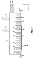
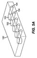
図1を参照すると、本発明に係る、基板20上への原子層堆積のための配送ヘッド10の一実施形態の側断面図が示されている。配送ヘッド10は、第一の気相材料を受けるためのインレットポートとして機能するガスインレット導管14、第二の気相材料を受けるインレットポートのためのガスインレット導管16、及び、第三の気相材料を受けるインレットポートのためのガスインレット導管18を有する。これらのガスはアウトプットチャンネル12を介して堆積アウトプット面36で射出され、そのアウトプットチャンネル12は下記に記載されるとおり、ディフューザーを含むことができる構造的配置を有する。図1及び続く図2〜3B中の波線矢印は配送ヘッド10から基板20へのガスの配送を示す。図1において、Xの矢印はガス廃棄物のための通路(この図中、上向きに示されている)を示し、排気ポートを提供する排気導管24に連通している排気チャンネル22が示されている。記載の単純化のために、ガス廃棄物は図2〜3Bには示していない。排気ガスはなおもある量の未反応前駆体を含みうるので、ある反応性種を主として含む排気フローを、別の種を主として含む排気フローと混合させることは望ましくないことがある。そのため、配送ヘッド10は幾つかの独立の排気ポートを含みうることが理解される。
Referring to FIG. 1, a cross-sectional side view of one embodiment of a
一実施形態において、ガスインレット導管14及び16はALD堆積を行うために基板表面上で順次に反応する第一のガス及び第二のガスを受けるようになっており、ガスインレット導管18は第一のガス及び第二のガスに対して不活性であるパージガスを受ける。配送ヘッド10は基板20から距離Dの空間を空けており、基板20は下記により詳細に記載されるとおり、基板支持体上に提供されうる。基板20と配送ヘッド10との間に往復運動を提供することができ、その往復運動は基板20の移動、配送ヘッド10の移動又は基板20と配送ヘッド10の両方の移動によって提供されうる。図1に示す特定の実施形態において、基板20は、図1中の矢印A及び基板20の右と左に架空の外周線によって示されるとおり、往復様式で堆積アウトプット面36を横切って基板支持体96によって移動される。往復運動は配送ヘッド10を用いた薄膜堆積に常に必要とされるわけではないことに注意すべきである。基板20及び配送ヘッド10の間の他のタイプの相対運動も提供されてよく、たとえば、下記により詳細に記載されるとおり、基板20又は配送ヘッド10の一方向又はそれ以上の方向への移動も提供されうる。
In one embodiment, the
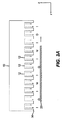
図2の断面図は配送ヘッド10の堆積アウトプット面36の部分にわたって射出されているガスフローを示している(上記のように排気通路は省略している)。この特定の配置において、各アウトプットチャンネル12は図1に見られるガスインレット導管14、16又は18のいずれかに気体流連通している。各アウトプットチャンネル12は、通常、第一の反応体気相材料O、又は、第二の反応体気相材料M又は第三の不活性気相材料Iを配送する。
2 shows the gas flow injected over the portion of the
図2は比較的に基本的又は単純なガスの配置を示している。複数の非金属堆積前駆体(たとえば、材料O)又は複数の金属含有前駆体材料(たとえば、材料M)を薄膜単一堆積において様々なポートで順に配送することができると考えられる。又は、反応体ガスの混合物、たとえば、金属前駆体材料の混合物、又は、金属前駆体と非金属前駆体の混合物は複合薄膜材料、たとえば、金属の交互の層を有するか又は金属酸化物材料中に混合された比較的に少量のドーパントを有する複合薄膜材料を製造するときに単一のアウトプットチャンネルで適用されうる。有意には、パージガスとも呼ぶ不活性ガスについてIと符号付けしたインターストリームはガスどうしが互いに反応する傾向がある反応体チャンネルを分離する。第一の反応体気相材料及び第二の反応体気相材料O及びMは互いに反応してALD堆積を行うが、反応体気相材料のO又はMのいずれも不活性気相材料Iと反応しない。図2及びこれ以降において使用されている用語は幾つかの典型的なタイプの反応体ガスを提示する。たとえば、第一の反応体気相材料Oは酸化性気相材料であることができ、第二の反応体気相材料Mは金属含有化合物、たとえば、亜鉛含有材料であることができる。不活性気相材料Iは窒素、アルゴン、ヘリウム又はALD装置でパージガスとして一般的に使用される他の気体であることができる。不活性気相材料Iは第一の反応体気相材料又は第二の反応体気相材料O及びMに対して不活性である。第一の反応体気相材料と第二の反応体気相材料との反応は、一実施形態において、半導体で使用されるZnO又はZnOなどの金属酸化物又は他の二元化合物を形成するであろう。二つより多くの反応体気相材料の反応によって、三元化合物、たとえば、ZnAlOを形成することができる。 FIG. 2 shows a relatively basic or simple gas arrangement. It is contemplated that multiple non-metal deposition precursors (eg, material O) or multiple metal-containing precursor materials (eg, material M) can be delivered sequentially at various ports in a thin film single deposition. Or a mixture of reactant gases, eg, a mixture of metal precursor materials, or a mixture of metal precursors and non-metal precursors, having composite thin film materials, eg, alternating layers of metals or in metal oxide materials It can be applied in a single output channel when manufacturing composite thin film materials with relatively small amounts of dopants mixed together. Significantly, an interstream labeled I for an inert gas, also called a purge gas, separates reactant channels where the gases tend to react with each other. The first reactant gas phase material and the second reactant gas phase material O and M react with each other to perform ALD deposition, but either O or M of the reactant gas phase material is an inert gas phase material I. no response. The terminology used in FIG. 2 and thereafter presents several typical types of reactant gases. For example, the first reactant gas phase material O can be an oxidizing gas phase material and the second reactant gas phase material M can be a metal-containing compound, such as a zinc-containing material. The inert gas phase material I can be nitrogen, argon, helium or other gases commonly used as purge gases in ALD equipment. The inert gas phase material I is inert with respect to the first reactant gas phase material or the second reactant gas phase material O and M. The reaction of the first reactant gas phase material and the second reactant gas phase material may in one embodiment form a metal oxide or other binary compound such as ZnO or ZnO used in a semiconductor. I will. The reaction of more than two reactant gas phase materials can form a ternary compound, such as ZnAlO.
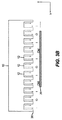
図3A及び3Bの断面図は、単純化された模式図の形で、ALDコーティング操作を示し、ALDコーティング操作は反応体気相材料O及びMを配送しているときに配送ヘッド10の堆積アウトプット面36にそって基板20を通過させるときに行われる。図3Aにおいて、基板20の表面は最初に、第一の反応体気相材料Oを配送するように指定されたアウトプットチャンネル12から連続的に射出される酸化性材料を受ける。ここで、基板の表面は部分的に反応した形の材料Oを含み、その材料は材料Mとの反応を受けやすい。その後、基板20が第二の反応体気相材料Mの金属化合物の通路を通過するときに、Mとの反応が起こり、金属酸化物又は2つの反応体気相材料から形成されうるある種の他の薄膜材料を形成する。従来の解決法とは異なり、図3A及び3Bに示される堆積シーケンスはパルス化されるのではなく、所与の基板又はその特定の領域に対して堆積の間に連続である。すなわち、材料O及びMは、基板20が配送ヘッド10の表面を横切って通過するときに又は、逆に、配送ヘッド10が基板20の表面を通過するときに、連続的に射出される。
The cross-sectional views of FIGS. 3A and 3B illustrate the ALD coating operation in simplified schematic form, where the ALD coating operation delivers the deposition output of the
図3A及び3Bが示すとおり、不活性気相材料Iは、第一の反応体気相材料Oのフロー及び第二の反応体気相材料Mのフローの間で、交互のアウトプットチャンネル12中に提供されうる。顕著には、図1に示したとおり、排気チャンネル22が存在するが、好ましくは、アウトプットチャンネル12の間に真空チャンネルは介在されない。少量の吸引を行う排気チャンネル22のみが、配送ヘッド10から射出されそして処理に使用された使用後ガスを通気させるために必要である。
As shown in FIGS. 3A and 3B, the inert gas phase material I is in the alternating
配送ヘッド10の操作の1つの態様は基板20に対するガス圧の提供に関し、分離距離Dが少なくとも部分的には課せられる圧力によって維持される。堆積アウトプット面36と基板20の表面との間にある量のガス圧力を維持することによって、本発明の装置は、配送ヘッド10自体、又は、基板20に対する空気支持、又は、より適切にはガス流体支持の少なくとも一部を提供する。この配置は、下記に記載されるように、配送ヘッド10のための輸送要求を単純化する助けになる。重要なことには、基板をガス圧によって支持するように配送ヘッドを基板に近接させることにより生じる効果はガスストリーム間の分離を助けることである。ヘッドをこれらのストリーム上で浮遊させることによって、圧力場は反応性及びパージフロー領域でセットアップされ、他のガスストリームと混合することがほとんどなく又は全くなく、インレットから排気にガスを送ることになる。
One aspect of the operation of the
一実施形態において、分離距離Dは比較的に小さいので、距離Dのわずかな変化でさえ(たとえば、100μmでさえ)、流速の有意な変化を要求し、そして結果として分離距離Dを提供しているガス圧力を要求する。たとえば、一実施形態において、1mm未満の変化を伴う分離距離Dを2倍にするには、分離距離Dを提供しているガスの流速を2倍より大きく、好ましくは4倍より大きくする必要がある。一般的な原則として、実施に際して分離距離Dを最小にし、結果的に、減じられた流速で操作することがより有利であると考えられる。 In one embodiment, the separation distance D is relatively small, so even a slight change in the distance D (eg, even 100 μm) requires a significant change in flow rate, and provides the separation distance D as a result. Requires gas pressure. For example, in one embodiment, to double the separation distance D with a change of less than 1 mm, the flow rate of the gas providing the separation distance D needs to be greater than twice, preferably greater than four times. is there. As a general principle, it is believed that it is more advantageous to minimize the separation distance D during operation and, consequently, operate at a reduced flow rate.
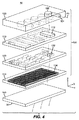
図4の分解図は、一実施形態における全体アセンブリーの小さな部分について、配送ヘッド10がどのように一連の孔付きプレートで構成されうるかを示し、そして複数のガスのうちの1つの一部分についてのみ例示のガスフロー通路を示している。配送ヘッド10についてのコネクションプレート100は配送ヘッド10の上流にあり、図4に図示していないガス供給源に連結するための一連のインプットポート104を有する。各インプットポート104は受け入れたガスを下流のガスチャンバープレート110に方向付ける方向付けチャンバー102に連結されている。ガスチャンバープレート110はサプライチャンバー112を有し、そのサプライチャンバー112はガス方向付けプレート120にある個々の方向付けチャンネル122とガスフロー連結されている。方向付けチャンネル122から、ガスフローはベースプレート130にある特に延長された排気チャンネル134に進行する。ガスディフューザーユニット140は拡散を行い、そして堆積アウトプット面36でインレットガスの最終の配送を行う。例示のガスフローF1は配送ヘッド10の各部品アセンブリーを通して追跡される。図4に示しているx−y−z軸の向きは本明細書の図5A及び7にも適用される。
The exploded view of FIG. 4 illustrates how the
図4の例に示すとおり、配送ヘッド10の配送アセンブリー150は重なった孔付きプレート:コネクションプレート100、ガスチャンバープレート110、ガス方向付けプレート120及びベースプレート130の配置として形成される。これらのプレートはこの「水平」実施形態において、堆積アウトプット面36に対して実質的に平行に配置される。ガスディフューザーユニット140も下記に記載されるように、重なった孔付きプレートから形成される。図4に示すプレートのいずれも、それ自体が、重なったプレートの積層物から形成されうることが理解できる。たとえば、適切に組み合わされた4枚又は5枚の積層された孔付きプレートからコネクションプレート100を形成することが有利であることがある。このタイプの配置は方向付けチャンバー102及びインプットポート104を形成するための機械加工法又は成形法よりも複雑でないことがある。
As shown in the example of FIG. 4, the
ガスディフューザーユニット140は基板に気相材料を提供するアウトプットチャンネルを通したフローを均一化するために使用することができる。同時係属の同一出願人の米国特許出願第11/620,740号明細書(発明の名称:DELIVERY DEVICE COMPRISING GAS DIFFUSER FOR THIN FILM DEPOSITION、参照により本明細書中に取り込む)は、場合により使用されうる様々なディフューザー装置を開示している。気相材料を拡散し及び/又は所望の背圧を提供するための他の手段が配送ヘッド内に代わりに提供されてもよい。さらに別の方法として、米国特許第4,413,022号明細書(Suntolaら、参照により本明細書中に取り込む)のように、ディフューザーなしに、アウトプットチャンネルを気相材料を提供するために使用することができる。未拡散フローを提供することにより、より高いスループットを達成することができるが、より低い均質性の堆積という犠牲を払う可能性がある。一方、ヘッドの浮遊を促進する配送デバイス内での背圧を提供することができるので、上記の浮遊ヘッド装置に対して、ディフューザー装置は特に有利である。
The
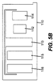
図5A〜図5Dは図4の実施形態における配送ヘッド10を形成するために組み合わせた主要部品の各々を示している。図5Aはコネクションプレート100の斜視図であり、複数の方向付けチャンバー102を示している。図5Bはガスチャンバープレート110の平面図である。サプライチャンバー113は一実施形態において配送ヘッド10のためのパージ又は不活性ガスのために使用される。サプライチャンバー115は一実施形態において前駆体ガス(O)の混合を提供し、排気チャンバー116はこの反応性ガスの排気通路を提供する。同様に、サプライチャンバー112はもう一つの必要な反応性ガスである金属前駆体ガス(M)を提供し、排気チャンバー114はこのガスの排気通路を提供する。
5A-5D show each of the major components combined to form the
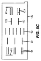
図5Cはこの実施形態における配送ヘッド10のためのガス方向付けプレート120の平面図である。金属前駆体材料(M)を提供する複数の方向付けチャンネル122は適切なサプライチャンバー112(この図に示していない)をベースプレート130に接続するようなパターンで配置される。対応する排気方向付けチャンネル123は方向付けチャンネル122付近に配置される。方向付けチャンネル90はもう一つの前駆体材料(O)を提供し、そして対応する排気方向付けチャンネル91を有する。方向付けチャンネル92はパージガス(I)を提供する。ここでも、図4及び5A〜5Dは1つの例示の実施形態を示し、多くの他の実施形態も可能であることを強調しなければならない。
FIG. 5C is a plan view of the
図5Dは配送ヘッド10のためのベースプレート130の平面図である。べースプレート130は排気チャンネル134が間に挿入された複数の延在射出チャンネル132を有する。
FIG. 5D is a plan view of the
図6は水平プレートから形成されたベースプレート130を示しそしてインプットポート104を示す斜視図である。図6の斜視図はアウトプット側から見たときのベースプレート130の外側表面を表し、ベースプレート130は延在射出チャンネル132及び延在排気チャンネル134を有する。図4を参照すると、図6の図はガスディフューザーユニット140に面する側から取ったものである。
FIG. 6 is a perspective view showing the
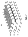
図7の分解図は図4の実施形態において及び下記に記載される他の実施形態において使用される、随意に存在しうるガスディフューザーユニット140の一実施形態を形成するために使用される部品の基本配置を示している。これらの部品は図8Aの平面図に示すノズルプレート142を含む。図6、7及び8Aの図面に示すように、ノズルプレート142はベースプレート130に対して取り付けられ、延在射出チャンネル132からのガスフローを得る。示した実施形態において、アウトプット通路143は必要とされる気相材料を提供する。順次の第一の排気スロット180は下記に記載されるように排気通路において提供される。
7 is an exploded view of the components used to form one embodiment of an optional
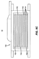
図8Bを参照すると、プレート142及び148(図7に示す)と共働して拡散するガスディフューザープレート146はノズルプレート142に対して取り付けられている。ノズルプレート142、ガスディフューザー146及びフェースプレート148の様々な通路の配置は必要量のガスフローの拡散を提供し、そして同時に、基板20の表面領域から離れる方向に排気ガスを効率的に方向付けるのに最適化されている。スロット182は排気ポートを提供する。示した実施形態において、第二のディフューザーアウトプット通路147を形成するガスサプライスロット及び排気スロット182はガスディフューザープレート146において交互になっている。
Referring to FIG. 8B, a
図8Cに示すとおり、フェースプレート148は、その後、基板20に対面する。ガスを提供するための第三のディフューザーアウトプット通路149及び排気スロット182もこの実施形態で交互になっている。
As shown in FIG. 8C, the
図8Dはガスディフューザーユニット140を通るガス配送通路に焦点が当てられており、図8Eは、対応して、ガス排気通路を示している。図8Dを参照すると、代表的なガスポートに組み合わせについて、一実施形態におけるアウトプットフローF2のための反応体ガスの徹底的な拡散のために使用される全体配置が示されている。ベースプレート130(図4)からのガスはノズルプレート142にある第一のアウトプット通路143を通して提供される。ガスは下流のガスディフューザープレート146にある第二のディフューザーアウトプット通路147に向かっていく。図8Dに示すとおり、一実施形態において、通路143と通路147との間に垂直オフセット(すなわち、図7に示す水平プレート配置を用い、垂直とは水平プレートの平面に対して法線方向)が存在することができ、それにより、背圧を発生させ、より均一なフローを容易に作り出す。その後、ガスはさらに下流のフェースプレート148にある第三のディフューザーアウトプット通路149に向かっていく。異なるアウトプット通路143,147及び149は空間的にずれているだけでなく、異なる幾何学形状を有し、それにより混合を最適化することができる。
FIG. 8D focuses on the gas delivery passage through the
随意のディフューザーユニットの非存在下に、ベースプレート中の延在射出チャンネル132は第三のディフューザーアウトプット通路149の代わりに配送ヘッド10のためのアウトプットチャンネル12として機能することができる。
In the absence of an optional diffuser unit, the
図8Eは、下流方向が供給ガスの場合と反対である同様の実施形態において、ガスを通気するために提供される排気パスを模式的にトレースしている。フローF3は順次の第三の排気スロット184、第二の排気スロット182及び第一の排気スロット180をそれぞれ通った通気ガスの通路を示す。ガスサプライのためのフローF2の回路のような混合パスとは異なり、図8E中に示す通気構成は表面からの使用済みガスの急速な移動が意図されている。このため、フローF3は基板表面から離れていく比較的に直接的な通気ガスである。
FIG. 8E schematically traces the exhaust path provided to vent the gas in a similar embodiment where the downstream direction is the opposite of that of the feed gas. Flow F3 shows vent gas passages through sequential
戻って図4を参照すると、コネクションプレート100、ガスチャンバープレート110、ガス方向付けプレート120及びベースプレート130として示している部品の組み合わせは配送アセンブリー150を提供するものとしてグループ分けできる。図4の図面及び座標軸配置を用いて、水平でなく垂直の孔付きプレートから形成される配送アセンブリーを含む配送アセンブリー150の別の実施形態が可能である。
Referring back to FIG. 4, the combination of components shown as
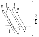
図9Aを参照すると、堆積アウトプット面36に対して垂直に配置された重なった孔付きプレートの積層体を用いた配送アセンブリー150に使用できる別の配列の底面図が示されている(すなわち、ガス射出面から見たもの)。説明の単純化のために、図9Aの「垂直形態」中に示す配送アセンブリー150の部分は2つの延在射出チャンネル152及び2つの延在排気チャンネル154を有する。図9A〜13Cの垂直プレート配列は多数の射出チャンネル及び排気チャンネルを提供するように容易に拡張することができる。図9A及び9Bのように、堆積アウトプット面36の平面に対して垂直に配置される孔付きプレートを用いて、各延在射出チャンネル152は下記に詳細に示すセパレータプレートと、そのセパレータプレートの間の中心にある反応体プレートで画定される側壁によって形成される。その後、孔の適当な位置合わせによって気相材料の供給源との流体連通が提供される。
Referring to FIG. 9A, there is shown a bottom view of another arrangement that can be used with a
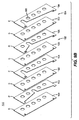
図9Bの分解図は図9Aに示している配送アセンブリー150の小さいセクションを形成するために使用される孔付きプレートの配置を示している。図9Cは、5つの射出ガス用延在チャンネル152を有し、積層された孔付きプレートを用いて形成された配送アセンブリー150を示す平面図である。次いで、図10A〜図13Cは様々な孔付きプレートを平面図及び斜視図の両方で示している。単純化のために、各タイプの孔付きプレートを文字で指定している:セパレータS、パージP、反応体R及び排気E。
The exploded view of FIG. 9B shows the arrangement of the perforated plates used to form the small section of the
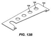
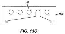
セパレータプレート160(S)が図9Bの左から右に示されており、また、図10A及び10Bにも示されている。セパレータプレートはガスを基板に向けて又は基板から離れていくように方向付けするために使用されるプレートの間に交互に存在する。パージプレート162(P)は図11A及び11Bに示されている。排気プレート164(E)は図12A及び12Bに示されている。反応体プレート166(R)は図13A及び13Bに示されている。図13Cは図13Aの反応体プレート166を水平にひっくり返すことにより得られる反応体プレート166’を示している。この交互の配向は必要ならば排気プレート164でも用いてよい。各孔付きプレートの孔168はプレートを重ねた際に整列しており、このため、図1を参照して説明したように、配送アセンブリー150を通してガスを延在射出アウトプットチャンネル152及び排気チャンネル154に通過させることができるダクトを形成する。
Separator plate 160 (S) is shown from left to right in FIG. 9B and is also shown in FIGS. 10A and 10B. Separator plates alternate between the plates used to direct the gas towards or away from the substrate. The purge plate 162 (P) is shown in FIGS. 11A and 11B. The exhaust plate 164 (E) is shown in FIGS. 12A and 12B. Reactor plate 166 (R) is shown in FIGS. 13A and 13B. FIG. 13C shows a reactant plate 166 'obtained by flipping the
図9Bに戻ると、配送アセンブリー150の一部のみが示されている。この部分のプレート構造は上記で指定した略文字を用いて示すことができる:すなわち、
S−P−S−E−S−R−S−E−(S)
(この配列の最後のセパレータプレートは図9A又は9Bには示していない)。この配列が示すとおり、セパレータプレート160(S)は側壁を形成することで各チャンネルを画定している。典型的なALD堆積のための2つの反応体ガスと必要なパージガスならびに排気チャンネルを提供するための最小配送アセンブリー150は下記の完全な略語シーケンスを用いて表される。
S−P−S−E1−S−R1−S−E1−S−P−S−E2−S−R2−S−E2−S−P−S−E1−S−R1−S−E1−S−P−S−E2−S−R2−S−E2−S−P−S−E1−S−R1−S−E1−S−P−S
Returning to FIG. 9B, only a portion of the
S-P-S-E-S-R-S-E- (S)
(The last separator plate in this arrangement is not shown in FIGS. 9A or 9B). As this arrangement shows, the separator plate 160 (S) defines each channel by forming sidewalls. A
S-P-S-E1-S-R1-S-E1-S-P-S-E2-S-R2-S-E2-S-P-S-E1-S-R1-S-E1-S- P-S-E2-S-R2-S-E2-S-P-S-E1-S-R1-S-E1-S-P-S
R1及びR2は使用される異なる2種の反応体ガスのための、異なる配向の反応体プレート166を表し、E1及びE2は対応して、異なる配向の排気プレート164を表す。
R1 and R2 represent differently oriented
排気プレート154は従来の意味の真空ポートである必要はなく、対応するアウトプットチャンネル12からフローを抜き出し、それにより、チャンネル内で均一フローパターンを促進するために単に供給されるものであってよい。隣接する延在射出チャンネル152のガス圧力の正反対の圧力より若干低い負の吸引で、均一なフローを促進させることができる。負の吸引は、たとえば、0.2〜1.0気圧の源(たとえば、真空ポンプ)での吸引圧で操作することができ、一方、典型的な真空は、たとえば、0.1気圧未満である。
The
配送ヘッド10により提供されるフローパターンを使用すると、堆積チャンバーに個々にガスをパルス化する、背景セクションで上述したような従来のアプローチに対して多くの利点がある。堆積装置の移動性が改良され、そして本発明の装置は基板の寸法が堆積ヘッドのサイズを超える高体積堆積用途に適する。流体動力学的性質も従来のアプローチよりも改良される。
Using the flow pattern provided by the
本発明で使用されるフロー構成では図1に示したとおり、配送ヘッド10と基板20との間の非常に小さい距離Dが可能になり、好ましくは1mm未満である。堆積アウトプット面36は基板表面に非常に近接して配置することができ、約1ミル(約0.025mm)以内とすることができる。近接配置は反応体ガスフローによって発生されるガス圧力によって容易になる。対照的に、CVD装置は有意に大きな分離距離を必要とする。上記で引用したYudovskyの米国特許第6,821,563号明細書に記載されているサイクル堆積などの以前のアプローチは基板表面に対する距離が0.5mm以上に限定されていたが、本発明の実施形態では0.5mm未満、たとえば、0.450mmで実施することができる。実際、基板表面に配送ヘッドをより近づけて配置することが本発明で好ましい。特に好ましい実施形態において、基板表面からの距離Dは0.20mm以下であることができ、好ましくは100μm未満である。
The flow configuration used in the present invention allows a very small distance D between the
積層プレートの実施形態において多数のプレートを組み立てる場合には、基板に送られるガスフローはガスフローを配送するすべてのチャンネル(I、M又はOチャンネル)にわたって均一である。これは孔付きプレートの適切な設計によって達成でき、たとえば、各射出アウトプットチャンネル又は排気チャンネルに再現可能な圧力損失を提供するように正確に機械加工された各プレートのフローパターンのある部分に流体制限を与えるなどによって達成されうる。一実施形態において、アウトプットチャンネル12は約10%以下の誤差範囲で、開口部の長さに沿って実質的に等価の圧力を示す。約5%以下の誤差又はさらには2%という小さい誤差を許容するような、より高度な許容限度を提供することもできる。
When assembling multiple plates in a laminated plate embodiment, the gas flow delivered to the substrate is uniform across all channels (I, M or O channels) that deliver the gas flow. This can be accomplished by proper design of the perforated plate, for example, by applying fluid to some part of the flow pattern of each plate precisely machined to provide reproducible pressure drop to each injection output channel or exhaust channel. This can be achieved by giving restrictions. In one embodiment, the
積層した孔付きプレートを用いる方法は本発明の物品を製造する特に有用な方法であるが、別の実施形態で有用であることができるこのような構造を製造する他の幾つかの方法が存在する。たとえば、装置は金属ブロックを直接的に機械加工することで製造でき、又は、幾つかの金属ブロックを互いに接着することで製造できる。さらに、内部成型形状を用いた成形技術も、当業者に理解されるとおり、使用されうる。装置はまた、いくつかの立体リソグラフィー技術のいずれかを用いて製造されうる。 While the method using laminated perforated plates is a particularly useful method of manufacturing the articles of the present invention, there are several other methods of manufacturing such structures that can be useful in alternative embodiments. To do. For example, the device can be manufactured by directly machining metal blocks, or it can be manufactured by bonding several metal blocks together. In addition, molding techniques using internally molded shapes can also be used, as will be appreciated by those skilled in the art. The device can also be manufactured using any of several stereolithographic techniques.
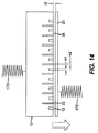
本発明の配送ヘッド10によって与えられる利点の1つは堆積アウトプット面36と基板20の表面との間に適切な分離距離(D)(図1)を維持することに関する。図14は、配送ヘッド10から射出されるガスフローの圧力を用いて距離Dを維持するための幾つかの重要な考慮点を示している。
One of the advantages provided by the
図14において、代表的な数のアウトプットチャンネル12及び排気チャンネル22を示している。1つ以上のアウトプットチャンネル12からの射出ガスの圧力はこの図で下向き矢印で示すとおりの力を発生している。この力が配送ヘッド10に有用なクッション又は「空気」支持(ガス流体支持)効果を与えるために、基板20に近接することができる、十分なランド面積、すなわち、堆積アウトプット面36にそった固体表面が存在しなければならない。ランド面積の百分率は堆積アウトプット面36の固体面積の相対量に対応しており、それにより、その下のガス圧力の蓄積が可能になる。最も単純な用語で、ランド面積は堆積アウトプット面36の合計面積−アウトプットチャンネル12及び排気チャンネル22の合計面積として計算できる。このことは幅w1のアウトプットチャンネル12又は幅w2の排気チャンネル22のガスフロー面積を除く合計面積をできるかぎり大きくしなければならないことを意味する。一実施形態において、95%のランド面積が提供される。他の実施形態は、たとえば、85%又は75%などの、より小さいランド面積値を用いる。分離力又はクッション力を変更しそれにより距離Dを変更するためにガスフロー速度の調節を用いることもできる。
In FIG. 14, a representative number of
配送ヘッド10が基板20上に距離Dを実質的に維持するように、ガス流体支持を提供することが有利であることが理解できる。これにより、あらゆる適切なタイプの輸送機構を用いても配送ヘッド10の本質的に摩擦を生じない移動が可能になる。配送ヘッド10は、配送ヘッド10が前後に導かれ、材料堆積の間に基板20の表面を横切ってさっと通過するときに、基板20の表面上を「浮遊」することができる。
It can be appreciated that it is advantageous to provide gas fluid support so that the
図14に示すとおり、配送ヘッド10は下方へのガス力が必要な分離を維持するために十分ではないほど重すぎることがある。このような場合には、スプリング170、磁石又は他のデバイスなどの補助リフティング部品を用いて持ち上げ力を補助することができる。他の場合には、逆の問題を生じるほどガス流が高すぎることがあり、それにより、追加の力を課さないと、基板20の表面から配送ヘッド10が大きな距離で離されすぎることがある。このような場合には、スプリング170は圧縮力を与えることができ、距離Dを維持するために追加の必要な力を提供する(図14の配置に対して下向き)。又は、スプリング170は下向きの力を補充するマグネット、エラストマースプリング又は他のデバイスであってよい。本発明のある実施形態において、配送ヘッド10は固定されていてよい。配送ヘッド10が固定されておりそして基板が浮遊されうる場合には、図14中にスプリング172によって示されるように、追加の力が基板20に適用されてよい。
As shown in FIG. 14, the
又は、配送ヘッド10は基板20に対して、特定の他の配向で配置されることができる。たとえば、基板20は空気支持効果によって重力に抗して支持されることができ、それにより、基板20は堆積の間に配送ヘッド10にそって移動されうる。基板20が配送ヘッド10の上方でクッションされている、基板20上での堆積のための空気支持効果を用いた一実施形態を図20に示す。
Alternatively, the
図20の別の実施形態は配送ヘッド10とガス流体支持98との間で方向Kで移動している基板20を示す。この実施形態において、配送ヘッド10は空気支持効果、又は、より適切には、ガス流体支持効果を有し、そして配送ヘッド10の堆積アウトプット面と基板20との間の望ましい距離Dを維持するためにガス流体支持98と共働している。ガス流体支持98は不活性ガスもしくは空気又はある他の気相材料のフローF4を用いて圧力を向けることができる。本堆積装置において、基板支持体又はホルダーは堆積の間に基板と接触していてよく、その基板支持体は基板を輸送する手段、たとえば、ローラーであってよい。このため、処理される基板の熱的遮断は本装置において必要ない。
Another embodiment of FIG. 20 shows the
堆積は反応性ガスの交互のシーケンスを示す堆積ヘッドの領域のみで起こるが、実際上の考慮によれば、堆積装置はコーティングセクションに基板を入れ又はコーティングセクションから基板を取り出し、また、図15の堆積装置60に示す堆積領域を超えて延びている基板の部分を場合により支持する領域を提供する、堆積ヘッドに隣接するセクションを有することが要求され、ここで、基板20の部分は拡大部分21a及び21bとして示される。定義の目的で、入り口セクション200は、基板の輸送方向を考慮して、堆積もしくはコーティングセクション220の前のセクションであり、出口セクション240は堆積もしくはコーティングセクション220の後のセクションである。
While deposition occurs only in the region of the deposition head that exhibits an alternating sequence of reactive gases, in practice considerations, the deposition apparatus places the substrate in or out of the coating section, and FIG. It is required to have a section adjacent to the deposition head that provides an area that optionally supports a portion of the substrate extending beyond the deposition area shown in the
堆積ヘッドはガス支持効果によって配送ヘッドを基板の近傍に維持しているので、入り口セクション及び出口セクションも同様の効果を用いることが便利である。これらのセクションは分配されたガス配送スロット(又は、より一般的にはポート)を有することができ、そのスロットは堆積セクションのものと非常に類似している。実際、入り口スロット及び出口スロットは、単一のガスのみを供給することを除いて、堆積領域のアウトプットスロットと同一であることがある環境下では可能である。 Since the deposition head maintains the delivery head in the vicinity of the substrate by a gas support effect, it is convenient to use a similar effect for the inlet and outlet sections. These sections can have distributed gas distribution slots (or more generally ports), which are very similar to those of the deposition section. In fact, the inlet and outlet slots are possible in an environment that may be identical to the output slot of the deposition area, except that only a single gas is supplied.
入り口セクション200及び出口セクション240には、薄膜の製造及び機能に悪影響を及ぼさない浮遊用ガスを供給することができる。多くの場合には、入り口セクション200及び出口セクション240用の浮遊ガスとして不活性ガスを使用することが望ましいことがある。又は、基板は堆積の前及び後に空気と遭遇する傾向があるので、場合によっては、これらのセクションの一方又は両方の浮遊ガスとして空気を使用することによってガス使用のコスト節約が達成されうる。
The
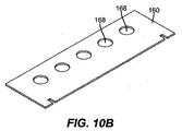
入り口セクション200及び出口セクション240は、場合により、追加のガス取り扱いを考慮することなく、単一のガス供給のみを用いることもできる。好ましい実施形態において、入り口セクション200及び出口セクション240の非堆積性アウトプット面には入り口セクション又は出口セクションの非堆積性アウトプット面にガスを供給する非堆積性アウトプット開口部252が配置されており、また、非堆積性アウトプット面の表面からガスを吸引するガス排気ポート254が配置されている。排気ポート254の使用により、より強固な基板の配置及び基板と非堆積性アウトプット面との適切なギャップの維持が可能である。
The
上記に示したとおり、入り口セクション200及び出口セクション240について、非堆積性アウトプット面はアウトプット開口部252及び排気ポート254を有することができ、それらは堆積もしくはコーティングセクションについて考えられるようなスロットの形態を取ることができる。しかしながら、これらの開口部はどんな便利な形状であってもよい。というのは、コーティングセクションとは対照的に、1つのタイプの開口部からのガスを別のタイプの開口部からのガスとを分離し、又は閉じ込めることがこれらのセクションでは要求さあれないからである。他のタイプの開口部の例は、幾つかを述べるとすると、正方形、五角形、又は、好ましくは円形の開口部がある。
As indicated above, for the
非堆積性アウトプット開口部252及び排気ポート254がスロットである場合には、スロットの好ましい配置では、各排気ポート又はチャンネル254は非堆積性アウトプット開口部252で各サイドが包囲され、また、同様に、各非堆積性アウトプット開口部252が各サイドで排気ポート254で包囲されている。好ましい実施形態において、入り口セクション及び出口セクションの最も遠い末端の開口部は非堆積性アウトプット開口部である。非堆積性アウトプット開口部252及び出口ポート254が円形開口部である場合には、これらの開口部は上記のタイプの交互の開口部を提供するような様式で配置できる。1つの好ましい配置は、各アウトプット開口部252が最も近い隣接部の排気ポート254で包囲されそして同様に各排気ポートは非堆積性アウトプット開口部252で包囲された正方形パターンの孔である。
If the
又は、入り口セクション及び出口セクションは非堆積性アウトプット面にガスを配送するために多孔性材料を用いることができる。 Alternatively, the inlet and outlet sections can use a porous material to deliver gas to the non-deposition output surface.
入り口セクション、出口セクション及びコーティングセクションは特定の予め選択された温度又は温度範囲に維持することができ、場合により、各セクションの異なる温度設定点とすることができる。 The inlet section, outlet section, and coating section can be maintained at specific preselected temperatures or temperature ranges, and in some cases can be a different temperature set point for each section.
コーティングヘッドからの交互のシーケンスのガスに繰り返して基板を暴露するいずれかの方法によって、膜のALD成長が起こるであろう。このような成長には従来技術において往復運動が考えられてきた。しかしながら、往復運動には、基板を載せそして基板の方向を繰り返し逆転させることができる複雑な機械装置が用いられる。往復運動でのあまり明確ではないがなおも大きな問題は、各ストロークの間に堆積領域から成長中の基板の少なくとも一部を引き出さなければならず、引き出された領域の制御されえない環境への暴露をもたらす可能性があることである。 Any method of repeatedly exposing the substrate to an alternating sequence of gases from the coating head will result in ALD growth of the film. Such growth has been conceived of reciprocating motion in the prior art. However, the reciprocating motion uses a complex mechanical device that can place a substrate and repeatedly reverse the direction of the substrate. A less obvious but still major problem with reciprocating motion is that during each stroke, at least a portion of the growing substrate must be pulled from the deposition area, leading to an uncontrolled environment of the extracted area. It can cause exposure.
上記の問題への本発明の解決法は、特定の薄膜のために要求される堆積量を受けるために、基板がコーティング領域を通した単一回の通過のみ又は単一回の二方向の通過のみを必要とする十分なALDサイクルのコーティング又は配送ヘッドを設計することを含む。このような形態では、1つの好ましい実施形態において、堆積目的で基板の方向を逆転させる必要なく、基板上のどの位置でも完全なALD成長を行うことができることが判る。 The solution of the present invention to the above problem is that the substrate is only a single pass through the coating region or a single bi-directional pass to receive the required deposition amount for a particular thin film. Design a coating or delivery head with a sufficient ALD cycle that only requires. In such a form, it can be seen that in one preferred embodiment, complete ALD growth can be performed anywhere on the substrate without having to reverse the orientation of the substrate for deposition purposes.
また、図15の実施形態の堆積装置60を再び参照すると、所望の厚さの完全な膜厚の完全な薄膜層は基板を入り口セクション200に入れ、基板を入り口セクション200からコーティングセクション220へそしてそれを通して輸送し、続けて基板を出口セクション240に輸送することで形成することができ、基板20は完成した薄膜とともに取り出すことができる。このことで、所望の膜厚が完成される前に基板をコーティング領域から取り出す理由がないという追加の利点がある。制御されない環境への暴露を回避することに加えて、単一回通過での連続成長は基板上のあらゆる所与の点での全体としての堆積速度を増加させるはずである。
Referring again to the
上記の一方向移動の別の利点は基板輸送に要求される機械装置が単純であることである。直線運動を生じさせるあらゆる種類の装置、たとえば、リニアモータ駆動リニアステージ、ロータリーモータ駆動リニアステージ、ベルトドライブ又は当業者に知られたとおりの直線運動を導入するあらゆる他の方法を使用して基板輸送を行うことができる。基板の移動を行う非接触方法も達成できる。このような方法として、方向付けされたガスストリームなどの粘性力、磁気力及び電気力が挙げられる。 Another advantage of the one-way movement described above is that the mechanical equipment required for substrate transport is simple. Substrate transport using any kind of device that produces linear motion, for example, linear motor driven linear stage, rotary motor driven linear stage, belt drive or any other method that introduces linear motion as known to those skilled in the art It can be performed. A non-contact method of moving the substrate can also be achieved. Such methods include viscous forces such as directed gas streams, magnetic forces and electrical forces.
装置は基板の方向を変更する必要がなく、ガス支持効果が低い摩擦力を生じさせるので、堆積領域を通る基板の輸送は、また、初期速度で基板を提供し、その後、その慣性によって少なくともある程度は堆積領域を通して基板を滑空させることで行える。基板に対する初期速度は上記の運動方法のいずれかによって与えることができる。 Since the apparatus does not need to change the orientation of the substrate and produces a frictional force with a low gas support effect, the transport of the substrate through the deposition area also provides the substrate at an initial speed and then at least in part due to its inertia. Can be done by gliding the substrate through the deposition area. The initial velocity for the substrate can be given by any of the above-described motion methods.
重力の効果により基板初期速度を与えることも可能である。このように、コーティングセクション、入り口セクション及び出口セクションは傾いていてよく、それにより、基板の運動の一部又はすべてを達成するために重力を与えることができる。さらに、これらのセクションの傾き角度は機械的に変更することができ、これにより、堆積の進行の間に、コーティングセクション、入り口セクション又は出口セクションの傾きを水平からあるレベルの傾きに変更することによって静止状態の基板を加速させることができる。 It is also possible to give the initial substrate speed by the effect of gravity. In this way, the coating section, the inlet section and the outlet section may be tilted so that gravity can be applied to achieve some or all of the movement of the substrate. In addition, the tilt angle of these sections can be changed mechanically, by changing the tilt of the coating section, inlet section or outlet section from horizontal to a certain level of tilt during the deposition process. A stationary substrate can be accelerated.
一方向の単一回の通過による堆積装置は基板輸送の単純さのために好ましいけれども、より小さい設置面積の堆積装置のためには二方向装置が好ましいことがある。二方向装置の場合には、入り口セクション及び出口セクションは一方向装置と同様の長さであるが、相対的に述べるならば、コーティングセクションはわずか半分の長さしか必要ない。再び図15を参照すると、このような実施形態において、基板20を入り口セクション200に入れ、コーティングセクション220へ入れそしてそれを通し、続けて基板を出口セクション240に入れ、基板の輸送方向を逆転させ、基板をコーティングセクション220に戻して通し、入り口セクション200に入れて輸送し、完成した薄膜とともに基板を取り出すことで所望の厚さの完全な薄膜層が形成できる。
While a one-way single pass deposition apparatus is preferred for simplicity of substrate transport, a two-way apparatus may be preferred for smaller footprint deposition apparatuses. In the case of a two-way device, the inlet and outlet sections are similar in length to the one-way device, but relatively speaking, the coating section needs only half the length. Referring again to FIG. 15, in such an embodiment, the
本発明のコーティングセクション220、入り口セクション200及び出口セクション240は多数の内部通路及び堆積アウトプット面開口部を有する複雑な機械装置である。しばしば、これらの装置は多数の結合された部品から形成されるであろう。さらに、単一回の通過による堆積を達成するために、コーティングセクションの長さ及び堆積アウトプット面スロットの数は非常に大きいことがある。たとえば、単一の堆積サイクルには8つの延在スロットが要求される:パージ−排気−第一の反応性ガス−排気−パージ−排気−第二の反応性ガス−排気。もし、単一の堆積サイクルが1Åの層厚を生じさせると仮定するならば、1000Åの層厚を達成するために、1000回の上記のサイクルが要求されるであろう。もし、各々の延在スロットがその隣接のものから0.025インチ離れているとさらに仮定するならば、堆積領域の合計長さは16.7フィートであろう。さらに、もし、入り口セクション及び出口セクションが基板を支持するために特定の合理的な長さである必要があるならば、これらのセクションは5フィートの長さを容易に超えることができるであろう。
The
このような大きな堆積領域を形成することは単一の一体物としての堆積ヘッドを形成することによって達成することが困難であることがある。幾つかの要因からこの困難さが生じる。まず第一に、このような長いヘッドは何千もの部品からなり、そしてうまくできたヘッドではこの多数の部品を、重大な欠陥又は許容されない欠陥を生じることなく、組み立てる必要があるであろう。さらに、非常に大きなヘッドを全体の堆積装置に取り付けそして取り扱うのに重大な問題があるであろう。最後に、もし、ヘッドが操作において損傷を受けるならば、単一の大きなヘッドを取り替えることは非常にコストが高くそして時間がかかるであろう。 Forming such a large deposition area can be difficult to achieve by forming the deposition head as a single unit. This difficulty arises from several factors. First of all, such a long head consists of thousands of parts, and a well-made head would need to assemble this many parts without causing serious or unacceptable defects. In addition, there will be significant problems in mounting and handling very large heads in the entire deposition apparatus. Finally, if the head is damaged in operation, replacing a single large head would be very costly and time consuming.
単一の大きな堆積ヘッドの代わりとなるのは独立のモジュールからヘッドを組み立てることである。モジュールは全セクションとすることができ、たとえば、入り口セクション、出口セクション又はコーティングセクションとすることができる。又は、所与のセクションは幾つかのモジュールから構成されることができる。図16はモジュール形態を用いる一実施形態の図を示す。図16において、入り口セクション200は4つのモジュール、202a、202b、202c及び202dからなる。堆積装置60のコーティングセクション220は5つのモジュール、222a、222b、222c、222d及び222eからなる。コーティングセクションの拡大部分は基板部分21cに対して近接している2つのモジュールを示しており、基板に対するモジュール面の位置のずれは改良された結果を得るための最大の望ましいずれ距離xx以内に維持される。これらのコーティングセクションモジュールは最終の堆積装置60の設計によって、同一であっても又は異なっていてもよい。実用上の目的で、複数のコーティングセクションモジュールの各々は単一のALDサイクルを完了するために適切な数のアウトプット開口部及び排気ポートを最小限含む。好ましくは、モジュールは1〜50の完全なALDサイクルが得られるように設計されている。図16は単一のモジュールを構成する出口セクション240を示している。最終の堆積装置の製造のためのモジュールの組み合わせが多く存在し、図16は単に例示の実施形態又は可能な配置を示すように与えられているにすぎず、その組み合わせは、もちろん、コーティングを行う特定の基板、特定のプロセス、関与する材料及び薄膜、ならびに、製造されるデバイスの特定のタイプによって決まり、そしてそれらに適合されるであろうということが当業者に理解されるはずである。
An alternative to a single large deposition head is to assemble the head from a separate module. A module can be an entire section, for example, an inlet section, an outlet section, or a coating section. Alternatively, a given section can consist of several modules. FIG. 16 shows a diagram of one embodiment using a modular configuration. In FIG. 16, the
1つの好ましい実施形態において、堆積装置は、たとえば、コーティングセクションに8又はそれ以上のモジュールを含み、好ましくは10〜100個のモジュールを含む。このようなモジュールの各々は実質的に別個にかつ独立に製造され、組み立てられそして堆積装置に配置される配送ヘッドを含むことができる。 In one preferred embodiment, the deposition apparatus includes, for example, 8 or more modules in the coating section, preferably 10 to 100 modules. Each such module can include a delivery head that is substantially separately and independently manufactured, assembled, and placed in a deposition apparatus.
モジュールの数がコーティングセクションを製造するのに収率にどのように影響を及ぼすことができるかを理解するために、8000のプレートから構成されるコーティングセクションの例を考える。200枚のプレートを組み立てる際に、アセンブリー中に2%の確率で欠陥を有するような欠陥率がアセンブリー中にあるものと仮定する。各200枚のプレートのモジュールとしてこのセクションを組み立てる際に、40個の動作モジュールが要求され、それゆえ、40個の使用可能なモジュールを生じるためには約41個のモジュールを組み立てることが必要であろう(約2%の廃棄加工品)。8000のプレートの単一の構造物を試みると、単一の構造物の動作の確率は0.9840=44%。結果として、1つの動作セクションを得るために約2つの完全なコーティングセクションが要求される(約50%の廃棄加工品)。本発明の一実施形態の本モジュールの態様はその問題を有意に回避し又は低減することができる。 To understand how the number of modules can affect the yield for manufacturing the coating section, consider the example of a coating section consisting of 8000 plates. Assume that when assembling 200 plates, there is a defect rate in the assembly that has a 2% probability of having defects in the assembly. When assembling this section as a module of 200 plates each, 40 motion modules are required, so it is necessary to assemble approximately 41 modules to produce 40 usable modules. Wow (approx. 2% waste products). Attempting a single structure of 8000 plates, the probability of single structure operation is 0.98 40 = 44%. As a result, about two complete coating sections are required to obtain one working section (about 50% waste product). The aspects of the module of an embodiment of the present invention can significantly avoid or reduce that problem.
好ましい実施形態において、本発明のコーティングセクション、入り口セクション及び出口セクションはすべてガス支持効果を用いて操作する。そのため、基板と堆積ヘッドとの間の分離は非常に小さくすることができ、ときに10ミクロンという小ささである。それゆえ、セクションの堆積アウトプット面は表面に不連続性がないことが非常に重要である。モジュール形態では、図16のコーティングセクションで例示されているセクションのモジュールは良好に位置合わせされた堆積アウトプット面を有しなければならない。この位置合わせを行いそして位置/高さの不整合が非常に小さくなるように、図16の挿入物の距離xxは小さくする必要がある。距離xxは10ミクロン未満にすべきであり、好ましくは5ミクロン未満であり、さらにより好ましくは2ミクロン未満である。 In a preferred embodiment, the coating section, inlet section and outlet section of the present invention are all operated using a gas support effect. Therefore, the separation between the substrate and the deposition head can be very small, sometimes as small as 10 microns. Therefore, it is very important that the deposition output surface of the section has no surface discontinuities. In modular form, the module in the section illustrated in the coating section of FIG. 16 must have a well-aligned deposition output surface. In order to perform this alignment and the position / height mismatch is very small, the insert distance xx of FIG. 16 needs to be small. The distance xx should be less than 10 microns, preferably less than 5 microns, and even more preferably less than 2 microns.
モジュールの適切な高さ配置を行うために幾つかの方法がある。モジュールを個々に位置調節手段の上に取り付けることができ、そして、所与のモジュールを設置するときに、位置調節手段を用いて、堆積アウトプット面の高さをある望ましい位置に調節することができる。高さ調節手段の例としては回転式マイクロメータポジショナー、焦電性ポジショナー及び当業界で既知の他の手段がある。 There are several ways to ensure proper module height placement. Modules can be individually mounted on top of the positioning means, and when installing a given module, the positioning means can be used to adjust the height of the deposition output surface to some desired position. it can. Examples of height adjustment means include rotary micrometer positioners, pyroelectric positioners and other means known in the art.
しばしば、単一の材料からなる薄膜をコーティングすることが望ましい。しかしながら、異なる材料の幾つかの層を含む完成膜が有用である薄膜が望ましい場合がある。モジュールコーティングセクションの場合、コーティングセクション内にある複数のモジュールが異なるガスを配送し、このため、すべてのモジュールが同一のコーティングを生じるものでないことも可能である。図17は、コーティングセクションのモジュールが異なる堆積化学物質を配送する堆積装置60の一実施形態を示している。コーティングセクション220は9個のモジュールから構成される。モジュール232aは第一の薄膜材料を形成する化学物質を配送するようになっており、モジュール232bは第二の薄膜材料を形成する化学物質を配送するようになっており、そしてモジュール232cは第三の薄膜材料を形成する化学物質を配送するようになっている。モジュール232a、232b及び232cは、出口セクション240に入る完成薄膜コーティングがそれぞれ第一の薄膜材料332a、第二の薄膜材料332b及び第三の薄膜材料332cの交互の薄膜層を全体の複数層の薄膜構造330(基板部分21dに対して示されている)に含むように配置されている。これらの層の各層の厚さはコーティングセクション220の対応するモジュール内のALDサイクルの数によって決定される。第一の材料、第二の材料及び第三の材料は上述のとおりのこのALD堆積装置を用いて適切に堆積されうるいかなる材料であってもよいことは当業者に理解されるべきである。図17は限定するものと解釈されるべきでなく、複数の薄膜を形成するための1つの可能な構成として作用すべきである。図17の出口セクション240、及び入り口セクション200のモジュール202a〜202dは上記の図面で説明したものと同様である。
Often it is desirable to coat a thin film of a single material. However, a thin film may be desirable where a finished film containing several layers of different materials is useful. In the case of a module coating section, it is possible that multiple modules within the coating section deliver different gases, so that not all modules produce the same coating. FIG. 17 illustrates one embodiment of a
平らな基板をコーティングする目的では、一般に、コーティング装置の堆積アウトプット面も平らであるものと考えられる。しかし、ある程度の曲率を有する堆積アウトプット面を有することが有利である可能性がある。 For the purpose of coating a flat substrate, it is generally considered that the deposition output surface of the coating apparatus is also flat. However, it may be advantageous to have a deposition output surface with a certain degree of curvature.
表面の曲率は一般に曲面の半径によって定義されうる。曲面の半径は円の一部が堆積アウトプット面の曲面に整合する円の半径である。表面の曲面が変化し、単一の半径で記載できない場合には、最大の曲面及び最小の曲面の半径を用いて、装置の曲面の特性半径を規定することができる。 The curvature of the surface can generally be defined by the radius of the curved surface. The radius of the curved surface is the radius of a circle where part of the circle matches the curved surface of the deposition output surface. If the curved surface changes and cannot be described with a single radius, the radius of the largest curved surface and the smallest curved surface can be used to define the characteristic radius of the curved surface of the device.
特定の基板では、基板の移動方向において特定の曲率の配送ヘッドを有することが有用なことがある。このことは、ヘッドの曲率がコーティングセクションの堆積アウトプット面から離れる方向に基板の前方縁を引っ張る傾向があるので、基板の前方縁に基板の残りの部分よりも小さい下向きの力を持たせることができるという有益な効果を有することができる。 For certain substrates, it may be useful to have a delivery head with a specific curvature in the direction of substrate movement. This is because the head curvature tends to pull the front edge of the substrate away from the deposition output surface of the coating section, so that the front edge of the substrate has a lower downward force than the rest of the substrate. Can have a beneficial effect.
ある基板では、基板の移動方向に垂直の方向に曲率を有することが有用なことがある。この曲率は波状効果を有し、基板の剛性を増加し、そしてより強健なコーティングをもたらす。 For some substrates, it may be useful to have curvature in a direction perpendicular to the direction of substrate movement. This curvature has a wavy effect, increases the stiffness of the substrate and results in a more robust coating.
モジュールタイプの堆積装置の場合、個々のモジュールの表面は曲面であっても又は曲面でなくてもよい。図18は堆積の間の基板の所望の弧に適合する弧に沿ってモジュールを配置しそして回転させる曲面堆積領域の例を示している。図18の部品は図16の部品に対応するが、モジュールに対して与えられる曲面はモジュールの曲面支持体250に整合している。
In the case of a module type deposition apparatus, the surface of each module may or may not be a curved surface. FIG. 18 shows an example of a curved deposition area in which the module is positioned and rotated along an arc that matches the desired arc of the substrate during deposition. The parts of FIG. 18 correspond to the parts of FIG. 16, but the curved surface provided to the module is aligned with the
あるプロセスにおいてある材料を堆積させるために、基板を加熱することが有利であることがある。図19A及び19Bは堆積装置の一実施形態の部品としてそれぞれ輻射式熱源及び対流式熱源を示している。輻射式熱源260は図19Aに示すようなIRランプ265、あるいは、石英ハロゲンランプのような当該技術分野において知られたあらゆる輻射式熱源から作られていてよい。図19Bに示す対流式熱源270は熱風ブロアを用いることができる。又は、対流式熱源270は冷風ブロアを用いて、基板を冷却するために用いることができる。図19A及び19Bの他の部品は図19A及び19Bに関して上述した部品を除いては図16の部品に対応する。本発明の装置はある実施形態において、室温又は室温付近の温度を含む広い範囲の温度にわたって基板上で堆積を行うことができる能力の点で利点がある。本発明の装置は真空環境で操作することができるが、大気圧又は大気圧付近の圧力での操作に特に適している。
It may be advantageous to heat the substrate to deposit a material in a process. 19A and 19B show a radiant heat source and a convective heat source, respectively, as components of one embodiment of the deposition apparatus. The radiant heat source 260 may be made from any radiant heat source known in the art such as an
好ましい実施形態において、ALDは大気圧又は大気圧付近の圧力及び広い範囲の雰囲気温度及び基板温度で、好ましくは、300℃未満の温度で行うことができる。好ましくは、汚染の可能性を最小にするために比較的にクリーンな環境が必要であった。しかし、本発明の装置の好ましい実施形態を用いるときに良好な性能を得るために完全な「クリーンルーム」条件又は不活性ガス充填包囲状態は必要ない。 In a preferred embodiment, ALD can be performed at or near atmospheric pressure and a wide range of ambient and substrate temperatures, preferably below 300 ° C. Preferably, a relatively clean environment was required to minimize the possibility of contamination. However, complete “clean room” conditions or inert gas filled enclosures are not required to obtain good performance when using preferred embodiments of the apparatus of the present invention.
図15をもう一度参照すると、原子層堆積(ALD)装置60は、比較的に良好に制御されそして汚染物のない環境を提供するためのチャンバー又はハウジング(図示しない)を場合により有することができる。堆積装置60は、また、供給ライン(図示していない)を通してコーティングセクション220に第一、第二及び第三の気相材料を提供するためのガスサプライ(図示していない)を含むことができる。好ましくは、これらのサプライラインは急速開放機構を有することができるであろう。また、その排気ラインも好ましくは急速開放機構を有する。単純化のために、随意に存在しうる真空蒸気回収装置及び他の補助部品は図15に示していないが、それらも使用することができる。このような蒸気回収装置は入り口セクション200及び出口セクション240において使用されるガスをリサイクルするために使用することができる。輸送副装置(図示していない)は入り口セクション200、コーティングセクション220及び出口セクション240の非堆積性アウトプット面に沿って基板20を輸送することができ、それは本開示で使用される座標軸系を用いてx軸方向に移動させる。移動制御ならびにバルブ及びその他の補助部品の全体の制御は、コンピュータ又は他の専用マイクロプロセッサーアセンブリーなどの制御ロジックプロセッサー、たとえば、PLC又はプログラム可能なロジックコンピュータによって与えられることができる。このようなコンピュータを用いたプロセス制御を堆積装置において用いて、コーティングセクションを通す単一回の一方向の通過で基板を移動させている間のみで、基板上に薄膜堆積を提供することができる。コーティングセクションに基板を通して移動させるため手段によって一方向の移動が提供されうる。又は、このような一方向の移動は薄膜堆積の間の配送ヘッドの機能又は操作が堆積装置を通した各基板の移動と組み合わせて制御されるプロセス制御デバイス又はスキームによっても少なくとも部分的に提供されうる。
Referring once again to FIG. 15, the atomic layer deposition (ALD)
ウェブ製造に特に有用であることができる別の実施形態において、ALD装置は多数の配送ヘッド又はデュアル配送ヘッドであって、その配送ヘッドが堆積を受ける基板の両側に配置されるものを有することができる。可とう性材料の可とう性配送ヘッドを1つ置きに提供することもできる。これにより、堆積表面に少なくともある程度のコンフォーマル性(共形性)を示す堆積装置を提供する。 In another embodiment that may be particularly useful for web manufacturing, the ALD apparatus may have multiple delivery heads or dual delivery heads, the delivery heads being located on either side of the substrate to be deposited. it can. It is also possible to provide every other flexible delivery head of flexible material. This provides a deposition apparatus that exhibits at least some conformality (conformality) on the deposition surface.
さらに別の実施形態において、配送ヘッドの1つ以上のアウトプットチャンネルを用いて上記において引用しそして参照により取り込んだ米国特許出願第11/392,006号明細書によって開示されている横方向ガスフロー配置を用いることができる。このような実施形態において、配送ヘッドと基板との間の分離を支持するガス圧は、たとえば、パージガスを射出するチャンネル(図2〜3BにIとして示しているチャンネル)などの幾つかのアウトプットチャンネルによって維持されうる。次いで、反応体ガスを射出する1つ以上のアウトプットチャンネル(図2〜3BにO又はMとして示しているチャンネル)のために横方向のフローを用いる。 In yet another embodiment, the lateral gas flow disclosed by US patent application Ser. No. 11 / 392,006, cited above and incorporated by reference, using one or more output channels of the delivery head. An arrangement can be used. In such an embodiment, the gas pressure that supports the separation between the delivery head and the substrate may be several outputs such as, for example, a channel (indicated as I in FIGS. 2-3B) for injecting purge gas. Can be maintained by channel. The lateral flow is then used for one or more output channels (channels shown as O or M in FIGS. 2-3B) that inject reactant gas.
又、基板の表面から配送ヘッドを少なくとも部分的に分離するために空気支持効果を用いることができるが、配送ヘッドの堆積アウトプット面から基板を持ち上げ又は空中に浮揚させるために本発明の装置を代わりに用いることができる。たとえば、プラテンを含む他のタイプの基板ホルダーを代わりに用いることができる。 An air support effect can also be used to at least partially separate the delivery head from the surface of the substrate, but the apparatus of the present invention can be used to lift or levitate the substrate from the deposition output surface of the delivery head. Can be used instead. For example, other types of substrate holders including platens can be used instead.
部品リスト
10 配送ヘッド
12 アウトプットチャンネル
14,16,18 ガスインレット導管
20 基板
21a,21b,21c,21d 基板の部分
22 排気チャンネル
24 排気導管
36 堆積アウトプット面
60 原子層堆積(ALD)装置
90 前駆体材料の方向付けチャンネル
91 排気方向付けチャンネル
92 パージガスの方向付けチャンネル
96 基板支持体
98 ガス流体支持
100 コネクションプレート
102 方向付けチャンバー
104 インプットポート
110 ガスチャンバープレート
112,113,115 サプライチャンバー
114,116 排気チャンバー
120 ガス方向付けプレート
122 前駆体材料の方向付けチャンネル
123 排気方向付けチャンネル
130 ベースプレート
132 延在射出チャンネル
134 延在排気チャンネル
140 ガスディフューザーユニット
142 ノズルプレート
143,147,149 第一、第二、第三のディフューザーアウトプット通路
146 ガスディフューザープレート
148 フェースプレート
150 配送アセンブリー
152 延在射出チャンネル
154 延在排気チャンネル
160 セパレータプレート
162 パージプレート
164 排気プレート
166,166’ 反応体プレート
168 開口部
170,172 スプリング
180 順次の第一の排気スロット
182 順次の第二の排気スロット
184 順次の第三の排気スロット
200 入り口セクション
202a,202b,202c,202d 入り口セクションモジュール
220 コーティングセクション
222a,222b,222c,222d,222e コーティングセクションモジュール
232a 第一の薄膜材料に適合したモジュール
232b 第二の薄膜材料に適合したモジュール
232c 第三の薄膜材料に適合したモジュール
240 出口セクション
250 モジュールのための曲面支持体
252 アウトプット開口部
254 排気ポート
260 輻射式熱源
265 IRランプ
270 対流式熱源
330 完成した薄膜
332a 第一の薄膜材料の薄膜
332b 第二の薄膜材料の薄膜
332c 第三の薄膜材料の薄膜
A 矢印
D 距離
E 排気プレート
F1,F2,F3,F4 ガスフロー
H 高さ
I 第三の不活性気相材料
K 方向
M 第二の反応体気相材料
O 第一の反応体気相材料
P パージプレート
R 反応体プレート
S セパレータプレート
X 矢印
Parts List 10 Delivery Head 12 Output Channel 14, 16, 18 Gas Inlet Conduit 20 Substrate 21a, 21b, 21c, 21d Substrate 22 Exhaust Channel 24 Exhaust Conduit 36 Deposition Output Surface 60 Atomic Layer Deposition (ALD) Device 90 Precursor Body material directing channel 91 Exhaust directing channel 92 Purge gas directing channel 96 Substrate support 98 Gas fluid support 100 Connection plate 102 Orienting chamber 104 Input port 110 Gas chamber plate 112,113,115 Supply chamber 114,116 Exhaust Chamber 120 Gas directing plate 122 Precursor material directing channel 123 Exhaust directing channel 130 Base plate 132 Extended injection channel 134 Extended exhaust channel 140 Gas diffuser unit 142 Nozzle plate 143, 147, 149 First, second and third diffuser output passages 146 Gas diffuser plate 148 Face plate 150 Delivery assembly 152 Extended injection channel 154 Extended exhaust channel 160 Separator plate 162 Purge plate 164 Exhaust plate 166, 166 'Reactor plate 168 Opening 170, 172 Spring 180 Sequential first exhaust slot 182 Sequential second exhaust slot 184 Sequential third exhaust slot 200 Inlet section 202a, 202b, 202c, 202d Entrance section module 220 Coating section 222a, 222b, 222c, 222 , 222e Coating section module 232a Module adapted to the first thin film material 232b Module adapted to the second thin film material 232c Module adapted to the third thin film material 240 Exit section 250 Curved support for module 252 Output opening Part 254 Exhaust port 260 Radiation heat source 265 IR lamp 270 Convective heat source 330 Completed thin film 332a First thin film material thin film 332b Second thin film material thin film 332c Third thin film material thin film A Arrow D Distance E Exhaust plate F1, F2, F3, F4 Gas flow H Height I Third inert gas phase material K direction M Second reactant gas phase material O First reactant gas phase material P Purge plate R Reactor plate S Separator Plate X Arrow
Claims (35)
(A)入り口セクション、
(B)(i)それぞれ第一の気相材料、第二の気相材料及び第三の気相材料のための第一の源、第二の源及び第三の源を少なくとも含む、それぞれ複数の気相材料のための複数の源、
(ii)薄膜堆積を受ける基板に前記複数の気相材料を配送するための配送ヘッドであって、
(a)前記第一の気相材料、第二の気相材料及び第三の気相材料をそれぞれ受けるための第一のインレットポート、第二のインレットポート及び第三のインレットポートを少なくとも含む、複数のインレットポート、及び、
(b)前記基板から距離をおいて離れた堆積アウトプット面であって、前記第一の気相材料、第二の気相材料及び第三の気相材料の各々のための実質的に平行に延在しているアウトプット開口部を含む、堆積アウトプット面、
を含み、前記堆積アウトプット面におけるアウトプット開口部から、前記第一の気相材料、第二の気相材料及び第三の気相材料を同時に配送するように設計されている配送ヘッド、
を含むコーティングセクション、
(C)出口セクション、
(D)前記コーティングセクションを通る一方向通路に前記基板を移動させるための手段、及び、
(E)薄膜堆積の間に、前記基板の表面と、前記配送ヘッドの堆積アウトプット面との間に実質的に均一な距離を維持するための手段、
を含み、
前記コーティングセクション中の配送ヘッドは、薄膜堆積のための基板表面への1つ以上の気相材料のフローを提供するとともに、基板表面から配送ヘッドの堆積アウトプット面を分離する力の少なくとも一部をも提供するように設計されており、
場合により、入り口セクション及び/又は出口セクションは、堆積装置の通路の少なくとも一部を通過している間に、基板の表面に非反応性ガスのガスフローを提供するように設計された、複数の非堆積性アウトプット開口部を有する非堆積性アウトプット面を各々含み、
前記配送ヘッドはコーティングセクションを通して単一回の一方向の通過での基板の移動の間のみで基板上に薄膜堆積を行うように設計されている、堆積装置。 A deposition apparatus for sequentially depositing a thin film of a solid material on a substrate,
(A) Entrance section,
(B) (i) a plurality of each including at least a first source, a second source and a third source for the first gas phase material, the second gas phase material and the third gas phase material, respectively. Multiple sources for gas phase materials,
(ii) a delivery head for delivering the plurality of vapor phase materials to a substrate undergoing thin film deposition,
(a) including at least a first inlet port, a second inlet port and a third inlet port for receiving the first gas phase material, the second gas phase material and the third gas phase material, respectively. Multiple inlet ports, and
(b) a deposition output surface spaced from the substrate and substantially parallel for each of the first vapor phase material, the second vapor phase material and the third vapor phase material; A deposition output surface, including an output opening extending to
A delivery head designed to simultaneously deliver the first vapor phase material, the second vapor phase material and the third vapor phase material from an output opening in the deposition output surface,
Including coating section,
(C) Exit section,
(D) means for moving the substrate into a one-way path through the coating section; and
(E) means for maintaining a substantially uniform distance between the surface of the substrate and the deposition output surface of the delivery head during thin film deposition;
Including
The delivery head in the coating section provides a flow of one or more vapor phase materials to the substrate surface for thin film deposition and at least a portion of the force separating the delivery output surface of the delivery head from the substrate surface. Is also designed to provide
In some cases, the inlet section and / or the outlet section are designed to provide a gas flow of non-reactive gas to the surface of the substrate while passing through at least a portion of the passage of the deposition apparatus. Each including a non-depositing output surface having a non-depositing output opening;
The deposition apparatus, wherein the delivery head is designed to deposit a thin film on a substrate only during the movement of the substrate in a single unidirectional pass through the coating section.
(A)基板を入り口セクションに輸送すること、
(B)前記基板を前記入り口セクションからコーティングセクションに輸送すること、
(C)前記基板を前記コーティングセクションを通して輸送すること、ここで、前記コーティングセクションは、(i)それぞれ第一の気相材料、第二の気相材料及び第三の気相材料のための第一の源、第二の源及び第三の源を少なくとも含む、それぞれ複数の気相材料のための複数の源、
(ii)薄膜堆積を受ける基板に前記気相材料を配送するための配送ヘッドであって、
(a)前記第一の気相材料、第二の気相材料及び第三の気相材料をそれぞれ受けるための第一のインレットポート、第二のインレットポート及び第三のインレットポートを少なくとも含む、複数のインレットポート、及び、
(b)前記基板から距離をおいて離れた堆積アウトプット面であって、前記第一の気相材料、第二の気相材料及び第三の気相材料の各々のための複数の実質的に平行に延在しているアウトプット開口部を含む、堆積アウトプット面、
を含み、前記堆積アウトプット面におけるアウトプット開口部から、前記第一の気相材料、第二の気相材料及び第三の気相材料を同時に配送するように設計されている配送ヘッド、
を含み、薄膜堆積の間に、前記配送ヘッドの堆積アウトプット面と基板表面との間は実質的に均一な距離が維持されており、薄膜堆積のための基板表面への配送ヘッドからの1つ以上の気相材料のフローは基板表面から配送ヘッドのアウトプット面を分離するための力の少なくとも一部を提供する、及び、
(D)前記コーティングセクションから少なくとも部分的に出口セクション中に前記基板を輸送すること、
を含み、
少なくとも1種の薄膜材料の所望の厚さの完成した薄膜は、基板を入り口セクションからコーティングセクションを通して出口セクションに単一回、一方向に通過させることで、又は、基板を入り口セクションからコーティングセクションを通して出口セクションに一回のみ通過させ、そしてコーティングセクションを通して入口セクションに一回のみ戻すことにより、単一回、二方向に通過させることで、前記基板上に形成される、方法。 A method for depositing a thin film of a solid material on a substrate, comprising:
(A) transport the substrate to the entry section;
(B) transporting the substrate from the entrance section to the coating section;
(C) transporting the substrate through the coating section, wherein the coating section comprises: (i) a first gas phase material, a second gas phase material, and a third gas phase material, respectively. A plurality of sources for each of a plurality of vapor phase materials, including at least one source, a second source and a third source;
(ii) a delivery head for delivering the vapor phase material to a substrate undergoing thin film deposition,
(a) including at least a first inlet port, a second inlet port and a third inlet port for receiving the first gas phase material, the second gas phase material and the third gas phase material, respectively. Multiple inlet ports, and
(b) a deposition output surface spaced from the substrate, wherein a plurality of substantial outputs for each of the first vapor phase material, the second vapor phase material and the third vapor phase material; A deposition output surface, including an output opening extending parallel to the
A delivery head designed to simultaneously deliver the first vapor phase material, the second vapor phase material and the third vapor phase material from an output opening in the deposition output surface,
A substantially uniform distance is maintained between the deposition output surface of the delivery head and the substrate surface during thin film deposition, and 1 from the delivery head to the substrate surface for thin film deposition. The flow of one or more vapor phase materials provides at least a portion of the force to separate the output surface of the delivery head from the substrate surface; and
(D) transporting the substrate from the coating section at least partially into the exit section;
Including
A finished thin film of the desired thickness of at least one thin film material can be obtained by passing the substrate from the inlet section through the coating section through the coating section in a single direction to the outlet section, or through the substrate through the coating section. A method of forming on the substrate by passing it through the outlet section only once and passing it through the coating section only once into the inlet section, in a single pass in two directions.
基板上で300℃以下の温度で金属酸化物をベースとする材料を少なくとも一層形成することを含み、該金属酸化物をベースとする材料は第一の反応性ガスが有機金属前駆体化合物を含みかつ第二の反応性ガスが反応性酸素含有気相材料を含む少なくとも2つの反応性ガスの反応生成物である、請求項24記載の方法。 Used to produce a semiconductor or dielectric thin film comprising a metal oxide based material for use in a transistor on a substrate;
Forming at least one layer of a metal oxide-based material on a substrate at a temperature of 300 ° C. or less, wherein the metal oxide-based material includes a first reactive gas comprising an organometallic precursor compound. 25. The method of claim 24, wherein the second reactive gas is a reaction product of at least two reactive gases comprising a reactive oxygen-containing gas phase material.
Applications Claiming Priority (2)
| Application Number | Priority Date | Filing Date | Title |
|---|---|---|---|
| US11/861,359 US8398770B2 (en) | 2007-09-26 | 2007-09-26 | Deposition system for thin film formation |
| PCT/US2008/010752 WO2009042044A1 (en) | 2007-09-26 | 2008-09-16 | Process and deposition system for thin film formation with gas delivery head having spatial separation of reactive gases and movement of the substrate passed the delivery head |
Publications (2)
| Publication Number | Publication Date |
|---|---|
| JP2010541236A true JP2010541236A (en) | 2010-12-24 |
| JP2010541236A5 JP2010541236A5 (en) | 2011-11-10 |
Family
ID=40099005
Family Applications (1)
| Application Number | Title | Priority Date | Filing Date |
|---|---|---|---|
| JP2010526893A Pending JP2010541236A (en) | 2007-09-26 | 2008-09-16 | Method and deposition apparatus for thin film formation using a gas delivery head that spatially separates reactive gases and with movement of a substrate through the delivery head |
Country Status (6)
| Country | Link |
|---|---|
| US (1) | US8398770B2 (en) |
| EP (1) | EP2191037A1 (en) |
| JP (1) | JP2010541236A (en) |
| CN (1) | CN101809193A (en) |
| TW (1) | TW200934886A (en) |
| WO (1) | WO2009042044A1 (en) |
Cited By (9)
| Publication number | Priority date | Publication date | Assignee | Title |
|---|---|---|---|---|
| JP2010540774A (en) * | 2007-09-26 | 2010-12-24 | イーストマン コダック カンパニー | Manufacturing method of optical film |
| JP2013506762A (en) * | 2009-09-30 | 2013-02-28 | サイノス・テクノロジー・インコーポレイテツド | Deposition reactor for forming a thin film on a curved surface |
| JP2014508225A (en) * | 2011-03-01 | 2014-04-03 | アプライド マテリアルズ インコーポレイテッド | Apparatus and process for atomic layer deposition |
| JP2014508221A (en) * | 2011-01-31 | 2014-04-03 | ネーデルランドセ・オルガニサティ・フォール・トゥーヘパスト−ナトゥールウェテンスハッペライク・オンデルズーク・テーエヌオー | Equipment for atomic layer deposition |
| KR20150120400A (en) * | 2013-02-20 | 2015-10-27 | 어플라이드 머티어리얼스, 인코포레이티드 | Apparatus and methods for carousel atomic layer deposition |
| KR101575844B1 (en) | 2014-05-09 | 2015-12-08 | 제주대학교 산학협력단 | Head for atomic layer deposition and atomic layer deposition device having the same |
| KR101787854B1 (en) | 2009-07-30 | 2017-10-18 | 네덜란제 오르가니자티에 포오르 토에게파스트-나투우르베텐샤펠리즈크 온데르조에크 테엔오 | Apparatus and method for atomic layer deposition |
| WO2017222350A1 (en) * | 2016-06-24 | 2017-12-28 | 주식회사 넥서스비 | Gas module for atomic layer deposition apparatus, atomic layer deposition apparatus, and atomic layer deposition method using same |
| JP2018160619A (en) * | 2017-03-23 | 2018-10-11 | 東芝メモリ株式会社 | Semiconductor manufacturing device |
Families Citing this family (97)
| Publication number | Priority date | Publication date | Assignee | Title |
|---|---|---|---|---|
| US11136667B2 (en) * | 2007-01-08 | 2021-10-05 | Eastman Kodak Company | Deposition system and method using a delivery head separated from a substrate by gas pressure |
| US20080166880A1 (en) * | 2007-01-08 | 2008-07-10 | Levy David H | Delivery device for deposition |
| US8211231B2 (en) * | 2007-09-26 | 2012-07-03 | Eastman Kodak Company | Delivery device for deposition |
| US8398770B2 (en) * | 2007-09-26 | 2013-03-19 | Eastman Kodak Company | Deposition system for thin film formation |
| US8182608B2 (en) * | 2007-09-26 | 2012-05-22 | Eastman Kodak Company | Deposition system for thin film formation |
| US7972898B2 (en) * | 2007-09-26 | 2011-07-05 | Eastman Kodak Company | Process for making doped zinc oxide |
| US9238867B2 (en) | 2008-05-20 | 2016-01-19 | Asm International N.V. | Apparatus and method for high-throughput atomic layer deposition |
| US20090291209A1 (en) | 2008-05-20 | 2009-11-26 | Asm International N.V. | Apparatus and method for high-throughput atomic layer deposition |
| US9048344B2 (en) | 2008-06-13 | 2015-06-02 | Kateeva, Inc. | Gas enclosure assembly and system |
| US8383202B2 (en) | 2008-06-13 | 2013-02-26 | Kateeva, Inc. | Method and apparatus for load-locked printing |
| US9604245B2 (en) | 2008-06-13 | 2017-03-28 | Kateeva, Inc. | Gas enclosure systems and methods utilizing an auxiliary enclosure |
| US10434804B2 (en) | 2008-06-13 | 2019-10-08 | Kateeva, Inc. | Low particle gas enclosure systems and methods |
| US10442226B2 (en) | 2008-06-13 | 2019-10-15 | Kateeva, Inc. | Gas enclosure assembly and system |
| US8899171B2 (en) | 2008-06-13 | 2014-12-02 | Kateeva, Inc. | Gas enclosure assembly and system |
| GB0816186D0 (en) * | 2008-09-05 | 2008-10-15 | Aviza Technologies Ltd | Gas delivery device |
| US20100037820A1 (en) * | 2008-08-13 | 2010-02-18 | Synos Technology, Inc. | Vapor Deposition Reactor |
| US8470718B2 (en) * | 2008-08-13 | 2013-06-25 | Synos Technology, Inc. | Vapor deposition reactor for forming thin film |
| EP2159304A1 (en) * | 2008-08-27 | 2010-03-03 | Nederlandse Organisatie voor toegepast- natuurwetenschappelijk onderzoek TNO | Apparatus and method for atomic layer deposition |
| EP3471130A1 (en) | 2008-12-04 | 2019-04-17 | Veeco Instruments Inc. | Chemical vapor deposition flow inlet elements and methods |
| FR2956869B1 (en) * | 2010-03-01 | 2014-05-16 | Alex Hr Roustaei | SYSTEM FOR PRODUCING HIGH CAPACITY FLEXIBLE FILM FOR PHOTOVOLTAIC AND OLED CELLS BY CYCLIC LAYER DEPOSITION |
| US8758512B2 (en) * | 2009-06-08 | 2014-06-24 | Veeco Ald Inc. | Vapor deposition reactor and method for forming thin film |
| US8657959B2 (en) * | 2009-07-31 | 2014-02-25 | E I Du Pont De Nemours And Company | Apparatus for atomic layer deposition on a moving substrate |
| US20110023775A1 (en) * | 2009-07-31 | 2011-02-03 | E.I. Du Pont De Nemours And Company | Apparatus for atomic layer deposition |
| US20110097490A1 (en) * | 2009-10-27 | 2011-04-28 | Kerr Roger S | Fluid distribution manifold including compliant plates |
| US20110097494A1 (en) * | 2009-10-27 | 2011-04-28 | Kerr Roger S | Fluid conveyance system including flexible retaining mechanism |
| US20110097493A1 (en) * | 2009-10-27 | 2011-04-28 | Kerr Roger S | Fluid distribution manifold including non-parallel non-perpendicular slots |
| US20110097488A1 (en) * | 2009-10-27 | 2011-04-28 | Kerr Roger S | Fluid distribution manifold including mirrored finish plate |
| US20110097492A1 (en) * | 2009-10-27 | 2011-04-28 | Kerr Roger S | Fluid distribution manifold operating state management system |
| US20110097491A1 (en) * | 2009-10-27 | 2011-04-28 | Levy David H | Conveyance system including opposed fluid distribution manifolds |
| US20110097489A1 (en) * | 2009-10-27 | 2011-04-28 | Kerr Roger S | Distribution manifold including multiple fluid communication ports |
| US20110097487A1 (en) * | 2009-10-27 | 2011-04-28 | Kerr Roger S | Fluid distribution manifold including bonded plates |
| EP2360293A1 (en) | 2010-02-11 | 2011-08-24 | Nederlandse Organisatie voor toegepast -natuurwetenschappelijk onderzoek TNO | Method and apparatus for depositing atomic layers on a substrate |
| EP2362002A1 (en) * | 2010-02-18 | 2011-08-31 | Nederlandse Organisatie voor toegepast -natuurwetenschappelijk onderzoek TNO | Continuous patterned layer deposition |
| EP2362411A1 (en) | 2010-02-26 | 2011-08-31 | Nederlandse Organisatie voor toegepast -natuurwetenschappelijk onderzoek TNO | Apparatus and method for reactive ion etching |
| NL2005049C2 (en) * | 2010-07-07 | 2012-01-10 | Levitech B V | Method and apparatus for contactlessly advancing substrates. |
| FI20105905A0 (en) * | 2010-08-30 | 2010-08-30 | Beneq Oy | Spray head and device |
| US8486192B2 (en) | 2010-09-30 | 2013-07-16 | Soitec | Thermalizing gas injectors for generating increased precursor gas, material deposition systems including such injectors, and related methods |
| US8133806B1 (en) | 2010-09-30 | 2012-03-13 | S.O.I.Tec Silicon On Insulator Technologies | Systems and methods for forming semiconductor materials by atomic layer deposition |
| JP5496073B2 (en) * | 2010-12-21 | 2014-05-21 | 三菱電機株式会社 | Microcrystalline semiconductor thin film manufacturing apparatus and microcrystalline semiconductor thin film manufacturing method |
| EP2481832A1 (en) * | 2011-01-31 | 2012-08-01 | Nederlandse Organisatie voor toegepast -natuurwetenschappelijk onderzoek TNO | Apparatus for atomic layer deposition |
| EP2481833A1 (en) | 2011-01-31 | 2012-08-01 | Nederlandse Organisatie voor toegepast -natuurwetenschappelijk onderzoek TNO | Apparatus for atomic layer deposition |
| US8840958B2 (en) * | 2011-02-14 | 2014-09-23 | Veeco Ald Inc. | Combined injection module for sequentially injecting source precursor and reactant precursor |
| US20120225207A1 (en) * | 2011-03-01 | 2012-09-06 | Applied Materials, Inc. | Apparatus and Process for Atomic Layer Deposition |
| US20120225203A1 (en) * | 2011-03-01 | 2012-09-06 | Applied Materials, Inc. | Apparatus and Process for Atomic Layer Deposition |
| EP2688850B1 (en) * | 2011-03-23 | 2018-02-21 | Pilkington Group Limited | Method of depositing zinc oxide coatings by chemical vapor deposition |
| TR201903701T4 (en) | 2011-03-23 | 2019-04-22 | Pilkington Group Ltd | The apparatus for deposition of thin film coatings and the deposition method for using this apparatus. |
| US20120269967A1 (en) * | 2011-04-22 | 2012-10-25 | Applied Materials, Inc. | Hot Wire Atomic Layer Deposition Apparatus And Methods Of Use |
| US9120344B2 (en) | 2011-08-09 | 2015-09-01 | Kateeva, Inc. | Apparatus and method for control of print gap |
| KR101780431B1 (en) * | 2011-08-09 | 2017-09-21 | 카티바, 인크. | Face-down printing apparatus and method |
| EP2557198A1 (en) | 2011-08-10 | 2013-02-13 | Nederlandse Organisatie voor toegepast -natuurwetenschappelijk onderzoek TNO | Method and apparatus for depositing atomic layers on a substrate |
| US10066297B2 (en) * | 2011-08-31 | 2018-09-04 | Alta Devices, Inc. | Tiled showerhead for a semiconductor chemical vapor deposition reactor |
| US9175393B1 (en) * | 2011-08-31 | 2015-11-03 | Alta Devices, Inc. | Tiled showerhead for a semiconductor chemical vapor deposition reactor |
| JP2013082959A (en) * | 2011-10-07 | 2013-05-09 | Sony Corp | Self-limiting reaction deposition apparatus and self-limiting reaction deposition method |
| JP5931091B2 (en) * | 2012-01-16 | 2016-06-08 | 株式会社アルバック | Deposition equipment |
| NL2008592C2 (en) * | 2012-04-03 | 2013-10-07 | Solaytec B V | Method for producing a photocell. |
| DE102012207172A1 (en) * | 2012-04-30 | 2013-10-31 | Osram Gmbh | DEVICE AND METHOD FOR THE SURFACE TREATMENT OF A SUBSTRATE AND METHOD FOR PRODUCING AN OPTOELECTRONIC COMPONENT |
| TWI565825B (en) * | 2012-06-07 | 2017-01-11 | 索泰克公司 | Gas injection components for deposition systems and related methods |
| US9512519B2 (en) * | 2012-12-03 | 2016-12-06 | Taiwan Semiconductor Manufacturing Company, Ltd. | Atomic layer deposition apparatus and method |
| TWI683382B (en) * | 2013-03-15 | 2020-01-21 | 應用材料股份有限公司 | Carousel gas distribution assembly with optical measurements |
| NL2010471C2 (en) * | 2013-03-18 | 2014-09-24 | Levitech B V | Substrate processing apparatus. |
| US9214254B2 (en) | 2013-09-26 | 2015-12-15 | Eastman Kodak Company | Ultra-thin AZO with nano-layer alumina passivation |
| TWI480406B (en) * | 2013-11-28 | 2015-04-11 | Metal Ind Res & Dev Ct | Deposition apparatus and conveyer module |
| WO2015100375A1 (en) | 2013-12-26 | 2015-07-02 | Kateeva, Inc. | Thermal treatment of electronic devices |
| JP6534390B2 (en) * | 2014-01-14 | 2019-06-26 | ザ バッテリーズ エスピー. ゼット オー.オー.The Batteries Sp. z o.o. | Thin film coating method and production line for its implementation |
| JP6113923B2 (en) | 2014-01-21 | 2017-04-12 | カティーバ, インコーポレイテッド | Apparatus and techniques for encapsulation of electronic devices |
| US9343678B2 (en) | 2014-01-21 | 2016-05-17 | Kateeva, Inc. | Apparatus and techniques for electronic device encapsulation |
| KR102390045B1 (en) | 2014-04-30 | 2022-04-22 | 카티바, 인크. | Gas cushion apparatus and techniques for substrate coating |
| CN104046960B (en) * | 2014-06-24 | 2016-08-17 | 北京七星华创电子股份有限公司 | A kind of gas distributor being applied to film deposition techniques |
| US11220737B2 (en) | 2014-06-25 | 2022-01-11 | Universal Display Corporation | Systems and methods of modulating flow during vapor jet deposition of organic materials |
| US11267012B2 (en) * | 2014-06-25 | 2022-03-08 | Universal Display Corporation | Spatial control of vapor condensation using convection |
| EP2960059B1 (en) | 2014-06-25 | 2018-10-24 | Universal Display Corporation | Systems and methods of modulating flow during vapor jet deposition of organic materials |
| MX2014013233A (en) * | 2014-10-30 | 2016-05-02 | Ct Investig Materiales Avanzados Sc | Injection nozzle for aerosols and their method of use to deposit different coatings via vapor chemical deposition assisted by aerosol. |
| JP6570147B2 (en) | 2014-11-26 | 2019-09-04 | カティーバ, インコーポレイテッド | Environmentally controlled coating system |
| KR102420015B1 (en) * | 2015-08-28 | 2022-07-12 | 삼성전자주식회사 | Shower head of Combinatorial Spatial Atomic Layer Deposition apparatus |
| US10566534B2 (en) | 2015-10-12 | 2020-02-18 | Universal Display Corporation | Apparatus and method to deliver organic material via organic vapor-jet printing (OVJP) |
| CH712199A1 (en) * | 2016-03-07 | 2017-09-15 | Fofitec Ag | Device for depositing thin layers on a substrate and roll material with a substrate having such layers. |
| US10294562B2 (en) | 2016-04-05 | 2019-05-21 | Aixtron Se | Exhaust manifold in a CVD reactor |
| US11174548B2 (en) | 2016-06-03 | 2021-11-16 | The Batteries Sp .Z.O.O. | Thin film coating method and the manufacturing line for its implementation |
| US10388721B2 (en) | 2017-01-24 | 2019-08-20 | International Business Machines Corporation | Conformal capacitor structure formed by a single process |
| US10501848B2 (en) | 2017-03-14 | 2019-12-10 | Eastman Kodak Company | Deposition system with modular deposition heads |
| US10550476B2 (en) | 2017-03-14 | 2020-02-04 | Eastman Kodak Company | Heated gas-bearing backer |
| US11248292B2 (en) | 2017-03-14 | 2022-02-15 | Eastman Kodak Company | Deposition system with moveable-position web guides |
| US20180265977A1 (en) | 2017-03-14 | 2018-09-20 | Eastman Kodak Company | Deposition system with vacuum pre-loaded deposition head |
| US10422038B2 (en) * | 2017-03-14 | 2019-09-24 | Eastman Kodak Company | Dual gas bearing substrate positioning system |
| US10895011B2 (en) | 2017-03-14 | 2021-01-19 | Eastman Kodak Company | Modular thin film deposition system |
| US10435788B2 (en) | 2017-03-14 | 2019-10-08 | Eastman Kodak | Deposition system with repeating motion profile |
| US10584413B2 (en) | 2017-03-14 | 2020-03-10 | Eastman Kodak Company | Vertical system with vacuum pre-loaded deposition head |
| US20180265970A1 (en) * | 2017-03-14 | 2018-09-20 | Eastman Kodak Company | Porous gas-bearing backer |
| US10400332B2 (en) * | 2017-03-14 | 2019-09-03 | Eastman Kodak Company | Deposition system with interlocking deposition heads |
| KR102595355B1 (en) | 2017-12-28 | 2023-10-30 | 삼성디스플레이 주식회사 | Deposition apparatus and depositon method using the same |
| JP7296699B2 (en) * | 2018-07-02 | 2023-06-23 | 東京エレクトロン株式会社 | GAS SUPPLY SYSTEM, PLASMA PROCESSING APPARATUS, AND GAS SUPPLY SYSTEM CONTROL METHOD |
| FR3084275B1 (en) * | 2018-07-30 | 2020-07-31 | Centre Nat Rech Scient | COMPACT HEAD AND STEAM DEPOSIT SYSTEM |
| US11306396B2 (en) * | 2018-11-30 | 2022-04-19 | Meidensha Corporation | Oxide film forming device |
| TW202045753A (en) * | 2019-06-04 | 2020-12-16 | 金碳洁股份有限公司 | Cyclic epitaxy deposition system |
| CN110791748A (en) * | 2019-10-15 | 2020-02-14 | 江苏卓高新材料科技有限公司 | Microporous film surface deposition device and method |
| WO2021119829A1 (en) * | 2019-12-18 | 2021-06-24 | Musselman Kevin P | Apparatus and method for thin film deposition |
| JP7098677B2 (en) | 2020-03-25 | 2022-07-11 | 株式会社Kokusai Electric | Manufacturing methods and programs for substrate processing equipment and semiconductor equipment |
Citations (6)
| Publication number | Priority date | Publication date | Assignee | Title |
|---|---|---|---|---|
| JPS63226917A (en) * | 1987-03-17 | 1988-09-21 | Fujitsu Ltd | Vapor-phase treatment system for semiconductor |
| JPH08239295A (en) * | 1995-03-03 | 1996-09-17 | Digital Ueebu:Kk | Production of crystal and apparatus therefor |
| JP2003324070A (en) * | 2002-04-30 | 2003-11-14 | Suzuki Motor Corp | Method and device of manufacturing thin film |
| JP2004319484A (en) * | 2003-04-11 | 2004-11-11 | Eastman Kodak Co | Method and device for forming transparent moisture-proof layer, and moisture-proof oled device |
| JP2005089781A (en) * | 2003-09-12 | 2005-04-07 | Mitsui Eng & Shipbuild Co Ltd | Thin film deposition system |
| JP2005109041A (en) * | 2003-09-29 | 2005-04-21 | Tadahiro Omi | Production device system |
Family Cites Families (56)
| Publication number | Priority date | Publication date | Assignee | Title |
|---|---|---|---|---|
| CH628600A5 (en) * | 1979-02-14 | 1982-03-15 | Siv Soc Italiana Vetro | PROCESS FOR CONTINUOUSLY DEPOSITING, ON THE SURFACE OF A SUBSTRATE CARRIED AT HIGH TEMPERATURE, A LAYER OF A SOLID MATERIAL AND INSTALLATION FOR THE IMPLEMENTATION OF THIS PROCESS. |
| FI57975C (en) | 1979-02-28 | 1980-11-10 | Lohja Ab Oy | OVER ANCHORING VIDEO UPDATE FOR AVAILABILITY |
| US4590042A (en) * | 1984-12-24 | 1986-05-20 | Tegal Corporation | Plasma reactor having slotted manifold |
| DE3869793D1 (en) * | 1987-01-27 | 1992-05-14 | Asahi Glass Co Ltd | GAS SUPPLY PIPE FOR REACTIVE DEPOSITION FROM THE GAS PHASE. |
| DE4011933C2 (en) * | 1990-04-12 | 1996-11-21 | Balzers Hochvakuum | Process for the reactive surface treatment of a workpiece and treatment chamber therefor |
| CA2016970A1 (en) * | 1990-05-16 | 1991-11-16 | Prasad N. Gadgil | Inverted diffusion stagnation point flow reactor for vapor deposition of thin films |
| US5136975A (en) * | 1990-06-21 | 1992-08-11 | Watkins-Johnson Company | Injector and method for delivering gaseous chemicals to a surface |
| US5122391A (en) * | 1991-03-13 | 1992-06-16 | Watkins-Johnson Company | Method for producing highly conductive and transparent films of tin and fluorine doped indium oxide by APCVD |
| DE69213340T2 (en) * | 1991-05-30 | 1997-03-27 | Hitachi Ltd | Valve and its use in a device made of semiconductor material |
| US5393563A (en) * | 1991-10-29 | 1995-02-28 | Ellis, Jr.; Frank B. | Formation of tin oxide films on glass substrates |
| US5413671A (en) * | 1993-08-09 | 1995-05-09 | Advanced Micro Devices, Inc. | Apparatus and method for removing deposits from an APCVD system |
| US5589002A (en) * | 1994-03-24 | 1996-12-31 | Applied Materials, Inc. | Gas distribution plate for semiconductor wafer processing apparatus with means for inhibiting arcing |
| US6022414A (en) * | 1994-07-18 | 2000-02-08 | Semiconductor Equipment Group, Llc | Single body injector and method for delivering gases to a surface |
| US6200389B1 (en) * | 1994-07-18 | 2001-03-13 | Silicon Valley Group Thermal Systems Llc | Single body injector and deposition chamber |
| US5688359A (en) * | 1995-07-20 | 1997-11-18 | Micron Technology, Inc. | Muffle etch injector assembly |
| JPH0945624A (en) * | 1995-07-27 | 1997-02-14 | Tokyo Electron Ltd | Leaf-type heat treating system |
| US5728224A (en) * | 1995-09-13 | 1998-03-17 | Tetra Laval Holdings & Finance S.A. | Apparatus and method for manufacturing a packaging material using gaseous phase atmospheric photo chemical vapor deposition to apply a barrier layer to a moving web substrate |
| JP3360265B2 (en) * | 1996-04-26 | 2002-12-24 | 東京エレクトロン株式会社 | Plasma processing method and plasma processing apparatus |
| US5938851A (en) * | 1997-04-14 | 1999-08-17 | Wj Semiconductor Equipment Group, Inc. | Exhaust vent assembly for chemical vapor deposition systems |
| US6126753A (en) * | 1998-05-13 | 2000-10-03 | Tokyo Electron Limited | Single-substrate-processing CVD apparatus and method |
| US6289842B1 (en) * | 1998-06-22 | 2001-09-18 | Structured Materials Industries Inc. | Plasma enhanced chemical vapor deposition system |
| US6206973B1 (en) * | 1999-04-23 | 2001-03-27 | Silicon Valley Group Thermal System Llc | Chemical vapor deposition system and method |
| US6245192B1 (en) * | 1999-06-30 | 2001-06-12 | Lam Research Corporation | Gas distribution apparatus for semiconductor processing |
| JP4487338B2 (en) * | 1999-08-31 | 2010-06-23 | 東京エレクトロン株式会社 | Film forming apparatus and film forming method |
| KR20010062209A (en) * | 1999-12-10 | 2001-07-07 | 히가시 데쓰로 | Processing apparatus with a chamber having therein a high-etching resistant sprayed film |
| US6503330B1 (en) * | 1999-12-22 | 2003-01-07 | Genus, Inc. | Apparatus and method to achieve continuous interface and ultrathin film during atomic layer deposition |
| JP3578398B2 (en) * | 2000-06-22 | 2004-10-20 | 古河スカイ株式会社 | Gas dispersion plate for film formation and method of manufacturing the same |
| CN1328766C (en) * | 2001-01-22 | 2007-07-25 | 东京毅力科创株式会社 | Process system and process method |
| SG94753A1 (en) * | 2001-02-06 | 2003-03-18 | Inst Of High Performance Compu | Microvalve devices |
| TW548724B (en) * | 2001-07-13 | 2003-08-21 | Asml Us Inc | Modular injector and exhaust assembly |
| KR20030038396A (en) * | 2001-11-01 | 2003-05-16 | 에이에스엠엘 유에스, 인코포레이티드 | System and method for preferential chemical vapor deposition |
| CN100362634C (en) * | 2002-01-24 | 2008-01-16 | 住友精密工业株式会社 | Ozone processing device |
| US6793733B2 (en) * | 2002-01-25 | 2004-09-21 | Applied Materials Inc. | Gas distribution showerhead |
| US20040065255A1 (en) * | 2002-10-02 | 2004-04-08 | Applied Materials, Inc. | Cyclical layer deposition system |
| US6821563B2 (en) * | 2002-10-02 | 2004-11-23 | Applied Materials, Inc. | Gas distribution system for cyclical layer deposition |
| US7064089B2 (en) | 2002-12-10 | 2006-06-20 | Semiconductor Energy Laboratory Co., Ltd. | Plasma treatment apparatus and method for plasma treatment |
| US7601223B2 (en) * | 2003-04-29 | 2009-10-13 | Asm International N.V. | Showerhead assembly and ALD methods |
| US20050103265A1 (en) * | 2003-11-19 | 2005-05-19 | Applied Materials, Inc., A Delaware Corporation | Gas distribution showerhead featuring exhaust apertures |
| US7456429B2 (en) * | 2006-03-29 | 2008-11-25 | Eastman Kodak Company | Apparatus for atomic layer deposition |
| US7413982B2 (en) * | 2006-03-29 | 2008-08-19 | Eastman Kodak Company | Process for atomic layer deposition |
| US7789961B2 (en) * | 2007-01-08 | 2010-09-07 | Eastman Kodak Company | Delivery device comprising gas diffuser for thin film deposition |
| US20080166880A1 (en) * | 2007-01-08 | 2008-07-10 | Levy David H | Delivery device for deposition |
| US11136667B2 (en) * | 2007-01-08 | 2021-10-05 | Eastman Kodak Company | Deposition system and method using a delivery head separated from a substrate by gas pressure |
| US8207063B2 (en) | 2007-01-26 | 2012-06-26 | Eastman Kodak Company | Process for atomic layer deposition |
| US7572686B2 (en) * | 2007-09-26 | 2009-08-11 | Eastman Kodak Company | System for thin film deposition utilizing compensating forces |
| US8030212B2 (en) * | 2007-09-26 | 2011-10-04 | Eastman Kodak Company | Process for selective area deposition of inorganic materials |
| US8211231B2 (en) * | 2007-09-26 | 2012-07-03 | Eastman Kodak Company | Delivery device for deposition |
| US20090079328A1 (en) * | 2007-09-26 | 2009-03-26 | Fedorovskaya Elena A | Thin film encapsulation containing zinc oxide |
| US7858144B2 (en) * | 2007-09-26 | 2010-12-28 | Eastman Kodak Company | Process for depositing organic materials |
| US7851380B2 (en) * | 2007-09-26 | 2010-12-14 | Eastman Kodak Company | Process for atomic layer deposition |
| US7972898B2 (en) * | 2007-09-26 | 2011-07-05 | Eastman Kodak Company | Process for making doped zinc oxide |
| US8398770B2 (en) * | 2007-09-26 | 2013-03-19 | Eastman Kodak Company | Deposition system for thin film formation |
| US8017183B2 (en) * | 2007-09-26 | 2011-09-13 | Eastman Kodak Company | Organosiloxane materials for selective area deposition of inorganic materials |
| US8182608B2 (en) * | 2007-09-26 | 2012-05-22 | Eastman Kodak Company | Deposition system for thin film formation |
| US20090081356A1 (en) * | 2007-09-26 | 2009-03-26 | Fedorovskaya Elena A | Process for forming thin film encapsulation layers |
| US20090095222A1 (en) * | 2007-10-16 | 2009-04-16 | Alexander Tam | Multi-gas spiral channel showerhead |
-
2007
- 2007-09-26 US US11/861,359 patent/US8398770B2/en active Active
-
2008
- 2008-09-16 CN CN200880109104A patent/CN101809193A/en active Pending
- 2008-09-16 JP JP2010526893A patent/JP2010541236A/en active Pending
- 2008-09-16 WO PCT/US2008/010752 patent/WO2009042044A1/en active Application Filing
- 2008-09-16 EP EP08834610A patent/EP2191037A1/en not_active Withdrawn
- 2008-09-25 TW TW097136923A patent/TW200934886A/en unknown
Patent Citations (6)
| Publication number | Priority date | Publication date | Assignee | Title |
|---|---|---|---|---|
| JPS63226917A (en) * | 1987-03-17 | 1988-09-21 | Fujitsu Ltd | Vapor-phase treatment system for semiconductor |
| JPH08239295A (en) * | 1995-03-03 | 1996-09-17 | Digital Ueebu:Kk | Production of crystal and apparatus therefor |
| JP2003324070A (en) * | 2002-04-30 | 2003-11-14 | Suzuki Motor Corp | Method and device of manufacturing thin film |
| JP2004319484A (en) * | 2003-04-11 | 2004-11-11 | Eastman Kodak Co | Method and device for forming transparent moisture-proof layer, and moisture-proof oled device |
| JP2005089781A (en) * | 2003-09-12 | 2005-04-07 | Mitsui Eng & Shipbuild Co Ltd | Thin film deposition system |
| JP2005109041A (en) * | 2003-09-29 | 2005-04-21 | Tadahiro Omi | Production device system |
Cited By (14)
| Publication number | Priority date | Publication date | Assignee | Title |
|---|---|---|---|---|
| JP2010540774A (en) * | 2007-09-26 | 2010-12-24 | イーストマン コダック カンパニー | Manufacturing method of optical film |
| KR101787854B1 (en) | 2009-07-30 | 2017-10-18 | 네덜란제 오르가니자티에 포오르 토에게파스트-나투우르베텐샤펠리즈크 온데르조에크 테엔오 | Apparatus and method for atomic layer deposition |
| KR101787773B1 (en) | 2009-07-30 | 2017-10-18 | 네덜란제 오르가니자티에 포오르 토에게파스트-나투우르베텐샤펠리즈크 온데르조에크 테엔오 | Apparatus and method for atomic layer deposition |
| JP2013506762A (en) * | 2009-09-30 | 2013-02-28 | サイノス・テクノロジー・インコーポレイテツド | Deposition reactor for forming a thin film on a curved surface |
| JP2014508221A (en) * | 2011-01-31 | 2014-04-03 | ネーデルランドセ・オルガニサティ・フォール・トゥーヘパスト−ナトゥールウェテンスハッペライク・オンデルズーク・テーエヌオー | Equipment for atomic layer deposition |
| JP2014508225A (en) * | 2011-03-01 | 2014-04-03 | アプライド マテリアルズ インコーポレイテッド | Apparatus and process for atomic layer deposition |
| JP2016510945A (en) * | 2013-02-20 | 2016-04-11 | アプライド マテリアルズ インコーポレイテッドApplied Materials,Incorporated | Apparatus and method for carousel atomic layer deposition |
| KR20170084363A (en) * | 2013-02-20 | 2017-07-19 | 어플라이드 머티어리얼스, 인코포레이티드 | Apparatus and methods for carousel atomic layer deposition |
| KR20150120400A (en) * | 2013-02-20 | 2015-10-27 | 어플라이드 머티어리얼스, 인코포레이티드 | Apparatus and methods for carousel atomic layer deposition |
| KR102147372B1 (en) | 2013-02-20 | 2020-08-24 | 어플라이드 머티어리얼스, 인코포레이티드 | Apparatus and methods for carousel atomic layer deposition |
| KR102201946B1 (en) | 2013-02-20 | 2021-01-11 | 어플라이드 머티어리얼스, 인코포레이티드 | Apparatus and methods for carousel atomic layer deposition |
| KR101575844B1 (en) | 2014-05-09 | 2015-12-08 | 제주대학교 산학협력단 | Head for atomic layer deposition and atomic layer deposition device having the same |
| WO2017222350A1 (en) * | 2016-06-24 | 2017-12-28 | 주식회사 넥서스비 | Gas module for atomic layer deposition apparatus, atomic layer deposition apparatus, and atomic layer deposition method using same |
| JP2018160619A (en) * | 2017-03-23 | 2018-10-11 | 東芝メモリ株式会社 | Semiconductor manufacturing device |
Also Published As
| Publication number | Publication date |
|---|---|
| TW200934886A (en) | 2009-08-16 |
| WO2009042044A1 (en) | 2009-04-02 |
| US20090081885A1 (en) | 2009-03-26 |
| EP2191037A1 (en) | 2010-06-02 |
| CN101809193A (en) | 2010-08-18 |
| US8398770B2 (en) | 2013-03-19 |
Similar Documents
| Publication | Publication Date | Title |
|---|---|---|
| JP2010541236A (en) | Method and deposition apparatus for thin film formation using a gas delivery head that spatially separates reactive gases and with movement of a substrate through the delivery head | |
| JP5346027B2 (en) | Deposition equipment for thin film formation | |
| US10351954B2 (en) | Deposition system and method using a delivery head separated from a substrate by gas pressure | |
| US8420168B2 (en) | Delivery device for deposition | |
| TWI419992B (en) | Delivery device for thin film deposition | |
| US20080166880A1 (en) | Delivery device for deposition | |
| US20110097493A1 (en) | Fluid distribution manifold including non-parallel non-perpendicular slots | |
| US20110097494A1 (en) | Fluid conveyance system including flexible retaining mechanism | |
| US20110097492A1 (en) | Fluid distribution manifold operating state management system | |
| US20110097489A1 (en) | Distribution manifold including multiple fluid communication ports | |
| US20110097490A1 (en) | Fluid distribution manifold including compliant plates | |
| US20110097487A1 (en) | Fluid distribution manifold including bonded plates | |
| US20110097491A1 (en) | Conveyance system including opposed fluid distribution manifolds | |
| US20110097488A1 (en) | Fluid distribution manifold including mirrored finish plate | |
| US20140206137A1 (en) | Deposition system for thin film formation |
Legal Events
| Date | Code | Title | Description |
|---|---|---|---|
| A521 | Written amendment |
Free format text: JAPANESE INTERMEDIATE CODE: A523 Effective date: 20110916 |
|
| A621 | Written request for application examination |
Free format text: JAPANESE INTERMEDIATE CODE: A621 Effective date: 20110916 |
|
| A977 | Report on retrieval |
Free format text: JAPANESE INTERMEDIATE CODE: A971007 Effective date: 20130424 |
|
| A131 | Notification of reasons for refusal |
Free format text: JAPANESE INTERMEDIATE CODE: A131 Effective date: 20130507 |
|
| A02 | Decision of refusal |
Free format text: JAPANESE INTERMEDIATE CODE: A02 Effective date: 20131008 |