JP2010539521A - Optical component, component manufacturing method, and optoelectronic device provided with the component - Google Patents
Optical component, component manufacturing method, and optoelectronic device provided with the component Download PDFInfo
- Publication number
- JP2010539521A JP2010539521A JP2010523267A JP2010523267A JP2010539521A JP 2010539521 A JP2010539521 A JP 2010539521A JP 2010523267 A JP2010523267 A JP 2010523267A JP 2010523267 A JP2010523267 A JP 2010523267A JP 2010539521 A JP2010539521 A JP 2010539521A
- Authority
- JP
- Japan
- Prior art keywords
- optical component
- molding material
- resin molding
- surface layer
- component
- Prior art date
- Legal status (The legal status is an assumption and is not a legal conclusion. Google has not performed a legal analysis and makes no representation as to the accuracy of the status listed.)
- Pending
Links
Images


Classifications
-
- C—CHEMISTRY; METALLURGY
- C08—ORGANIC MACROMOLECULAR COMPOUNDS; THEIR PREPARATION OR CHEMICAL WORKING-UP; COMPOSITIONS BASED THEREON
- C08J—WORKING-UP; GENERAL PROCESSES OF COMPOUNDING; AFTER-TREATMENT NOT COVERED BY SUBCLASSES C08B, C08C, C08F, C08G or C08H
- C08J7/00—Chemical treatment or coating of shaped articles made of macromolecular substances
- C08J7/12—Chemical modification
-
- H—ELECTRICITY
- H01—ELECTRIC ELEMENTS
- H01L—SEMICONDUCTOR DEVICES NOT COVERED BY CLASS H10
- H01L2224/00—Indexing scheme for arrangements for connecting or disconnecting semiconductor or solid-state bodies and methods related thereto as covered by H01L24/00
- H01L2224/01—Means for bonding being attached to, or being formed on, the surface to be connected, e.g. chip-to-package, die-attach, "first-level" interconnects; Manufacturing methods related thereto
- H01L2224/42—Wire connectors; Manufacturing methods related thereto
- H01L2224/47—Structure, shape, material or disposition of the wire connectors after the connecting process
- H01L2224/48—Structure, shape, material or disposition of the wire connectors after the connecting process of an individual wire connector
- H01L2224/4805—Shape
- H01L2224/4809—Loop shape
- H01L2224/48091—Arched
-
- H—ELECTRICITY
- H01—ELECTRIC ELEMENTS
- H01L—SEMICONDUCTOR DEVICES NOT COVERED BY CLASS H10
- H01L2224/00—Indexing scheme for arrangements for connecting or disconnecting semiconductor or solid-state bodies and methods related thereto as covered by H01L24/00
- H01L2224/01—Means for bonding being attached to, or being formed on, the surface to be connected, e.g. chip-to-package, die-attach, "first-level" interconnects; Manufacturing methods related thereto
- H01L2224/42—Wire connectors; Manufacturing methods related thereto
- H01L2224/47—Structure, shape, material or disposition of the wire connectors after the connecting process
- H01L2224/48—Structure, shape, material or disposition of the wire connectors after the connecting process of an individual wire connector
- H01L2224/481—Disposition
- H01L2224/48151—Connecting between a semiconductor or solid-state body and an item not being a semiconductor or solid-state body, e.g. chip-to-substrate, chip-to-passive
- H01L2224/48221—Connecting between a semiconductor or solid-state body and an item not being a semiconductor or solid-state body, e.g. chip-to-substrate, chip-to-passive the body and the item being stacked
- H01L2224/48245—Connecting between a semiconductor or solid-state body and an item not being a semiconductor or solid-state body, e.g. chip-to-substrate, chip-to-passive the body and the item being stacked the item being metallic
- H01L2224/48247—Connecting between a semiconductor or solid-state body and an item not being a semiconductor or solid-state body, e.g. chip-to-substrate, chip-to-passive the body and the item being stacked the item being metallic connecting the wire to a bond pad of the item
-
- H—ELECTRICITY
- H01—ELECTRIC ELEMENTS
- H01L—SEMICONDUCTOR DEVICES NOT COVERED BY CLASS H10
- H01L33/00—Semiconductor devices with at least one potential-jump barrier or surface barrier specially adapted for light emission; Processes or apparatus specially adapted for the manufacture or treatment thereof or of parts thereof; Details thereof
- H01L33/48—Semiconductor devices with at least one potential-jump barrier or surface barrier specially adapted for light emission; Processes or apparatus specially adapted for the manufacture or treatment thereof or of parts thereof; Details thereof characterised by the semiconductor body packages
- H01L33/52—Encapsulations
- H01L33/56—Materials, e.g. epoxy or silicone resin
Landscapes
- Chemical & Material Sciences (AREA)
- General Chemical & Material Sciences (AREA)
- Health & Medical Sciences (AREA)
- Chemical Kinetics & Catalysis (AREA)
- Medicinal Chemistry (AREA)
- Polymers & Plastics (AREA)
- Organic Chemistry (AREA)
- Led Device Packages (AREA)
- Casting Or Compression Moulding Of Plastics Or The Like (AREA)
- Encapsulation Of And Coatings For Semiconductor Or Solid State Devices (AREA)
Abstract
本発明は、規定された形態を有する光学コンポーネントに関する。この光学コンポーネントには、付着を低減する化学修飾された表面層を有する樹脂成形材料が含まれている。 The present invention relates to an optical component having a defined configuration. The optical component includes a resin molding material having a chemically modified surface layer that reduces adhesion.
Description
本発明は、規定の形態を有する光学コンポーネント、該コンポーネント製造方法および該コンポーネントが設けられた光電子素子に関する。 The present invention relates to an optical component having a specified form, a method for manufacturing the component, and an optoelectronic device provided with the component.
背景技術
本願は、ドイツ連邦共和国特許出願第102007041889.4号および第102007052133.4号の優先権を主張するものであり、その開示内容は参照により本願に含まれるものとする。
BACKGROUND This application claims the priority of German patent applications 1020070418899.4 and 102007052133.4, the disclosure of which is hereby incorporated by reference.
光電子素子内には、付着性の表面を有する光学コンポーネントが存在する可能性がある。このような表面によって、汚染物質または例えば塵埃のような粒子がその表面上に付着する、またはコンポーネント自体がほかのコンポーネントに付着するようになる。このような付着が品質上の問題を引き起こしてしまう。 There may be optical components within the optoelectronic device that have adherent surfaces. Such a surface allows contaminants or particles such as dust to adhere to the surface, or the component itself to adhere to other components. Such adhesion causes quality problems.
本発明の課題は、上述の欠点に関して改善された光学コンポーネントを提供することである。 The object of the present invention is to provide an improved optical component with respect to the above-mentioned drawbacks.
前記課題は、請求項1に記載の光学コンポーネントによって解決される。さらに別の請求項には、この光学コンポーネント製造方法およびそのコンポーネントが設けられた光電子素子について記載されている。 The object is solved by an optical component according to claim 1. Yet another claim describes this method of manufacturing an optical component and an optoelectronic device provided with the component.
本発明の実施形態によると、規定の形態を有する光学コンポーネントには、付着を低減する表面層を有する樹脂成形材料が含まれている。付着を低減するこの表面層は、化学修飾されている。したがって、この種の光学コンポーネントは粒子付着による汚染物質を低減する。 According to an embodiment of the present invention, an optical component having a defined form includes a resin molding material having a surface layer that reduces adhesion. This surface layer that reduces adhesion is chemically modified. Thus, this type of optical component reduces contaminants due to particle adhesion.
表面層と同じ樹脂成形材料からこのコンポーネントを成形することができる。この場合、表面層の樹脂成形材料は化学修飾されている。したがって、このコンポーネント上に付加層を配置する必要はなく、ただ樹脂成形材料の表面層を化学修飾によって形成すればよい。化学修飾として、表面層をフッ素化することができる。光学コンポーネントを例えば塵埃粒子に対して付着を低減するように構成することができる。 This component can be molded from the same resin molding material as the surface layer. In this case, the resin molding material of the surface layer is chemically modified. Therefore, it is not necessary to arrange an additional layer on this component, and the surface layer of the resin molding material may be formed by chemical modification. As a chemical modification, the surface layer can be fluorinated. The optical component can be configured to reduce adhesion to, for example, dust particles.
光学コンポーネントは光と相互に作用し、つまりはこのコンポーネントを光学活性的にさせるか、または光学的に操作することができる。したがって、光学コンポーネントは光を成形したり、光を案内したりまたは光を変換したりするように作用させることができる。光学コンポーネントは、その光学的な作用を例えば散乱、屈折、反射、偏向および回折の形態として有することができる。 The optical component interacts with the light, i.e. it can be made optically active or optically manipulated. Thus, the optical component can act to shape the light, guide the light, or convert the light. An optical component can have its optical effects in the form of scattering, refraction, reflection, deflection and diffraction, for example.
光学コンポーネントを放射に対して透過性または反射性にすることができる。それ故に、この光学コンポーネントを光電子素子内で使用することができる。そこにおいて、放出または受容される放射の放射路に透過性のコンポーネントを配置することができる。 The optical component can be transmissive or reflective to radiation. This optical component can therefore be used in optoelectronic devices. There, a transmissive component can be placed in the radiation path of the emitted or received radiation.
注型材料またはレンズとしてコンポーネントを成形することができる。それ故に、このコンポーネントは例えば光電子素子内の光学コンポーネントとして使用されるのに適している。このコンポーネントが注型材料として成形されている場合には、例えば半導体層列用の注型材料としてコンポーネントを使用することができる。 Components can be molded as casting materials or lenses. This component is therefore suitable for use as an optical component, for example in an optoelectronic device. If this component is molded as a casting material, it can be used, for example, as a casting material for a semiconductor layer sequence.
付着を低減する表面層を有する樹脂成形材料が含まれているレンズは、殊に温度および放射に対し安定しており、放出および受容される放射に対して透過性である。 Lenses containing a resin molding material having a surface layer that reduces adhesion are particularly stable to temperature and radiation and are transmissive to emitted and accepted radiation.
光学コンポーネント内に存在する樹脂成形材料には、シリコーン樹脂とエポキシ樹脂とシリコーン基および/またはエポキシ基を有する複合樹脂とを含有するグループから選択される材料が含まれている。これらの材料は透過性であり、注型材料またはレンズとして成形するのに適している。 The resin molding material present in the optical component includes a material selected from the group including a silicone resin, an epoxy resin, and a composite resin having a silicone group and / or an epoxy group. These materials are permeable and are suitable for molding as casting materials or lenses.
さらに本発明は、上述の特性を備えた光学コンポーネントの製造方法にも関する。すなわち、この種の方法は、A)樹脂成形材料を準備するステップと、B)樹脂成形材料を成形して光学コンポーネントを形成するステップと、C)光学コンポーネント上に樹脂成形材料の付着を低減する表面層を形成するステップとを含んでいる。この方法を所期のように比較的簡単に転換することができる。 The invention further relates to a method of manufacturing an optical component having the above-mentioned characteristics. That is, this type of method includes A) preparing a resin molding material, B) molding the resin molding material to form an optical component, and C) reducing adhesion of the resin molding material on the optical component. Forming a surface layer. This method can be changed relatively easily as expected.
この方法の場合、ステップA)において、シリコーン樹脂とエポキシ樹脂とシリコーン基および/またはエポキシ基を有する複合樹脂とを含有するグループから選択される樹脂成形材料を準備することができる。ステップB)において、レンズまたは注型材料として樹脂成形材料を成形することができる。成形するために、例えば射出成型法または注型法を使用することができる。これによって、所期のようにコンポーネントを所望の形態に形成することができる。 In the case of this method, in step A), a resin molding material selected from the group containing a silicone resin, an epoxy resin, and a composite resin having a silicone group and / or an epoxy group can be prepared. In step B), a resin molding material can be molded as a lens or casting material. For molding, for example, an injection molding method or a casting method can be used. As a result, the component can be formed into a desired shape as expected.
ステップC)において、付着を低減する表面層を形成するために、樹脂成形材料の表面層を化学修飾することができる。ステップC)において化学修飾するために、樹脂成形材料をプラズマにさらすことができる。このプラズマには、CF4,C2F6,NF3およびSF6を含むグループから選択可能なフッ素含有化合物を含有させることができる。これらの化合物はフッ素含有であり、シリコーン樹脂またはエポキシ樹脂をフッ素化するために用いられる。例えば樹脂成形材料中に含まれる炭素原子をフッ素化することができる。これによって、樹脂成形材料の表面に50nmよりわずかな厚さを有する薄層を形成するテフロン化合物が生じる。さらに、フッ素含有化合物を含むプラズマは、例えばアルゴンのような不活性ガスを含み、したがって、フッ素含有化合物を必要に応じて希釈する(verduennen)ことができる。この場合、アルゴン対フッ素含有化合物の割合を1:9と9:1の間とすることができる。1〜30分間、有利には5〜30分間、樹脂成形材料をプラズマにさらすことができる。このことを室温で行うことができ、この場合、プラズマ処理中40℃〜50℃まで樹脂成形材料を熱することができる。プラズマに低圧プラズマを含めることができるので、樹脂成形材料を約0.1mbarの圧力でプラズマにさらすことができる。 In step C), the surface layer of the resin molding material can be chemically modified in order to form a surface layer that reduces adhesion. The resin molding material can be exposed to plasma for chemical modification in step C). The plasma can contain a fluorine-containing compound that can be selected from the group comprising CF 4 , C 2 F 6 , NF 3 and SF 6 . These compounds contain fluorine and are used to fluorinate silicone resins or epoxy resins. For example, carbon atoms contained in the resin molding material can be fluorinated. This produces a Teflon compound that forms a thin layer having a thickness of less than 50 nm on the surface of the resin molding material. Furthermore, the plasma containing the fluorine-containing compound contains an inert gas, such as argon, so that the fluorine-containing compound can be diluted as needed. In this case, the ratio of argon to fluorine-containing compound can be between 1: 9 and 9: 1. The resin molding material can be exposed to the plasma for 1 to 30 minutes, preferably 5 to 30 minutes. This can be done at room temperature, in which case the resin molding material can be heated to between 40 ° C. and 50 ° C. during the plasma treatment. Since the plasma can include a low pressure plasma, the resin molding material can be exposed to the plasma at a pressure of about 0.1 mbar.
さらに、フッ素含有化合物はプラズマ処理中重合し、付加層として樹脂成形材料の修飾される表面層に析出されるということが可能となる。この付加層をテフロンの様にし、50nmよりわずかな厚さとすることができる。 Further, it becomes possible that the fluorine-containing compound is polymerized during the plasma treatment and deposited as an additional layer on the surface layer to be modified of the resin molding material. This additional layer can be made of Teflon and have a thickness slightly smaller than 50 nm.
さらに本発明は、放射を放出するまたは放射を受容する半導体層列と、上述の特性を備えた光学コンポーネントとが設けられている光電子素子に関する。この場合、光学コンポーネントは放出または受容される放射の放射路に配置されている。光電子素子は、レンズとして成形されている光学コンポーネントを含むことができる。さらにこの光電子素子は、注型材料として成形されている光学コンポーネントも含むことができる。この光電子素子は半導体層列を含むことができ、この場合、注型材料によって半導体層列が封入されている。この半導体層列は、例えば発光ダイオード(LED)であってもよい。 The invention further relates to an optoelectronic device provided with a semiconductor layer sequence emitting or receiving radiation and an optical component with the above-mentioned properties. In this case, the optical component is arranged in the radiation path of the emitted or received radiation. The optoelectronic element can include an optical component that is shaped as a lens. The optoelectronic device can also include an optical component that is molded as a casting material. The optoelectronic device can comprise a semiconductor layer sequence, in which case the semiconductor layer sequence is encapsulated by a casting material. This semiconductor layer sequence may be, for example, a light emitting diode (LED).
図面に基づき、本発明を詳細に説明する。 The present invention will be described in detail with reference to the drawings.
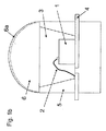
図1aには、光電子素子の概略側面図が示されている。この光電子素子には、半導体層列1が設けられており、これは例えばLEDであってもよく、直接でもボンディングワイヤ2を介してでもその都度導電ストリップ4と電子的にコンタクトされている。半導体層列並びにボンディングワイヤは、ケーシング5内にある注型材料3に囲まれている。ケーシング5には斜めにされた側面を設けることができ、この側面は、送出される放射の反射の改善に役立つ。注型材料3は、エポキシ樹脂とシリコーン樹脂とシリコーン基および/またはエポキシ基を有する複合樹脂とを含有する樹脂成形材料から成形することができ、例えばフッ素含有化合物を含むプラズマで処理されている。これによって、注型材料3には、例えば塵埃粒子のような汚染物質に対して付着を低減する表面層3aが含まれている。
FIG. 1a shows a schematic side view of an optoelectronic device. The optoelectronic element is provided with a semiconductor layer sequence 1, which may be, for example, an LED and is in electronic contact with the conductive strip 4 each time, either directly or via a
ケーシングおよび注型材料の上部には、レンズ6を設けることができる。このことは図1bに示されている。レンズ6には、エポキシ樹脂およびシリコーン樹脂を含む樹脂成形材料が含まれている。また、レンズとして成形される樹脂成形材料も次の方法で処理することができる。すなわち、例えばフッ素含有化合物を含むプラズマにレンズをさらす方法によって処理することができるのである。したがって、レンズにも付着を低減する表面層6aが含まれており、この表面層6aは、フッ素化化合物を含み、例えば塵埃のような汚染物質に対して付着を低減する。
A
図2には、樹脂成形材料から成形されまだ光電子素子に取り付けられていないレンズの写真が示されている。レンズは並びあって支持部材に取り付けられている。図2の個々の写真の配置は、ホルダ上のレンズの配置に相当する。第1の列Rのレンズは、処理されていない表面を有するシリコーン含有レンズである。第2の列Aおよび第3の列Bのレンズは、2つの製造物バッチ(Herstellungscharge)における上述の方法に対応してCF4プラズマで処理されひいては付着を低減する表面層を有するシリコーン含有レンズである。 FIG. 2 shows a photograph of a lens molded from a resin molding material and not yet attached to the optoelectronic element. The lenses are lined up and attached to the support member. The arrangement of the individual photographs in FIG. 2 corresponds to the arrangement of the lenses on the holder. The lenses in the first row R are silicone-containing lenses having an untreated surface. Second column A and the third row B lenses, two product batches silicone containing lenses having a surface layer treated with CF 4 plasma in response to the above-described method for reducing the turn attachment in (Herstellungscharge) is there.
下方から、エポキシ樹脂内に注入されたグラスファイバ織物(Glasfasergewebe)を含むレンズが、細かい塵埃の粒子で埃まみれにされている。このことは図2で矢印によって示されている。したがって全列において、一番下の行で最も多量の細かい塵埃がレンズ上に存在し、塵埃のソースからいっそう大きく間隔を取ると、つまり上部の行においてこの塵埃が除去される。しかしながら、処理されていない表面を有するレンズを用いた列Rにおいて、処理されたレンズを用いた行AおよびBの場合よりも著しく高い塵埃の濃度が生じている(白い面参照)。したがって、レンズ表面の処理によって付着を低減する表面層ひいては汚染物質に対して強いコンポーネントとなるということを示しているといえる。 From below, a lens containing glass fiber fabric (Glasfasergewebe) injected into an epoxy resin is dusted with fine dust particles. This is indicated by the arrows in FIG. Therefore, in all the rows, the finest amount of fine dust is present on the lens in the bottom row, and this dust is removed in the upper row when it is further spaced from the dust source. However, in column R using a lens having an untreated surface, a much higher dust concentration is produced than in the case of rows A and B using a treated lens (see white surface). Therefore, it can be said that the surface layer that reduces adhesion by the treatment of the lens surface, and thus a component resistant to contaminants.
図1および図2に示した例および実施形態を任意に変更することができる。さらに、本願はこれらの例に制限されず、ここでは記載されていないさらに別の実施形態も可能であるということを考慮することができる。 The examples and embodiments shown in FIGS. 1 and 2 can be arbitrarily changed. Further, it can be considered that the present application is not limited to these examples, and further embodiments not described herein are possible.
Claims (15)
付着を低減する化学修飾された表面層(3a,6a)を有する樹脂成形材料を含んでいることを特徴とする、
光学コンポーネント。 Has a prescribed form,
Characterized in that it contains a resin molding material having a chemically modified surface layer (3a, 6a) to reduce adhesion,
Optical component.
A)樹脂成形材料を準備するステップと、
B)前記樹脂成形材料を成形して光学コンポーネントを形成するステップと、
C)前記光学コンポーネント上に前記樹脂成形材料の付着を低減する表面層(3a,6a)を形成するステップ
とを含んでいることを特徴とする、
製造方法。 In the manufacturing method of the optical component of any one of Claim 1 to 8,
A) preparing a resin molding material;
B) molding the resin molding material to form an optical component;
C) forming a surface layer (3a, 6a) for reducing adhesion of the resin molding material on the optical component,
Production method.
光電子素子。 A semiconductor layer sequence emitting or receiving radiation and an optical component according to any one of claims 1 to 8 in the radiation path of the emitted or received radiation,
Optoelectronic device.
Applications Claiming Priority (3)
| Application Number | Priority Date | Filing Date | Title |
|---|---|---|---|
| DE102007041889 | 2007-09-04 | ||
| DE102007052133A DE102007052133A1 (en) | 2007-09-04 | 2007-10-31 | Optical component, method for producing the component and optoelectronic component with the component |
| PCT/DE2008/001353 WO2009030193A1 (en) | 2007-09-04 | 2008-08-14 | Optical component, method for producing said component, and optoelectronic assembly unit comprising said component |
Publications (2)
| Publication Number | Publication Date |
|---|---|
| JP2010539521A true JP2010539521A (en) | 2010-12-16 |
| JP2010539521A5 JP2010539521A5 (en) | 2012-02-16 |
Family
ID=40299222
Family Applications (1)
| Application Number | Title | Priority Date | Filing Date |
|---|---|---|---|
| JP2010523267A Pending JP2010539521A (en) | 2007-09-04 | 2008-08-14 | Optical component, component manufacturing method, and optoelectronic device provided with the component |
Country Status (8)
| Country | Link |
|---|---|
| US (1) | US8194326B2 (en) |
| EP (1) | EP2185952B1 (en) |
| JP (1) | JP2010539521A (en) |
| KR (1) | KR20100057042A (en) |
| CN (1) | CN101796435B (en) |
| DE (1) | DE102007052133A1 (en) |
| TW (1) | TWI382504B (en) |
| WO (1) | WO2009030193A1 (en) |
Cited By (1)
| Publication number | Priority date | Publication date | Assignee | Title |
|---|---|---|---|---|
| JP2015079926A (en) * | 2013-09-10 | 2015-04-23 | 旭化成ケミカルズ株式会社 | Optical device and manufacturing method of the same |
Families Citing this family (5)
| Publication number | Priority date | Publication date | Assignee | Title |
|---|---|---|---|---|
| WO2014155247A1 (en) * | 2013-03-27 | 2014-10-02 | Koninklijke Philips N.V. | Retrofit organic light emitting diode (oled) light source |
| CN107250227A (en) * | 2014-10-20 | 2017-10-13 | 道康宁东丽株式会社 | Optical component, optical semiconductor device and lighting apparatus |
| JP6446280B2 (en) * | 2015-01-28 | 2018-12-26 | 日立オートモティブシステムズ株式会社 | Electronic equipment |
| DE102015103335A1 (en) * | 2015-03-06 | 2016-09-08 | Osram Opto Semiconductors Gmbh | Optoelectronic device and method for producing an optoelectronic device |
| CN109411587B (en) * | 2018-12-10 | 2020-11-27 | 浙江单色电子科技有限公司 | Production method of purple light LED containing silica gel lens and purple light LED |
Citations (2)
| Publication number | Priority date | Publication date | Assignee | Title |
|---|---|---|---|---|
| JPS5599932A (en) * | 1979-01-24 | 1980-07-30 | Hitachi Ltd | Surface treatment of organic high polymer |
| JP2007051053A (en) * | 2005-07-21 | 2007-03-01 | Sony Corp | Metal oxide nanoparticle, method for producing the same, light-emitting element assembly, and optical material |
Family Cites Families (11)
| Publication number | Priority date | Publication date | Assignee | Title |
|---|---|---|---|---|
| US4125319A (en) * | 1976-05-03 | 1978-11-14 | Eastman Kodak Company | Active light control device |
| DE69624923T2 (en) * | 1995-08-11 | 2003-08-21 | Daikin Ind Ltd | ORGANIC FLUORINE POLYMERS CONTAINING SILICON AND THEIR USE |
| CN100530758C (en) * | 1998-03-17 | 2009-08-19 | 精工爱普生株式会社 | Thin film pattering substrate and surface treatment |
| ATE344805T1 (en) * | 1999-09-08 | 2006-11-15 | Daikin Ind Ltd | FLUORCHEMICAL ADHESIVE MATERIAL AND LAYERED PRODUCT OBTAINED THEREFROM |
| EP1487916A4 (en) * | 2002-03-07 | 2006-05-24 | Petroferm Inc | Dust repellant compositions |
| JP4506070B2 (en) * | 2002-11-01 | 2010-07-21 | コニカミノルタホールディングス株式会社 | Method for forming antiglare layer, method for producing antiglare film, and ink jet device for forming antiglare layer |
| DE102004019973B4 (en) * | 2004-02-29 | 2006-07-13 | Osram Opto Semiconductors Gmbh | Method for producing a contamination-protected, optoelectronic component and contamination-protected, optoelectronic component |
| JP4496394B2 (en) * | 2004-03-31 | 2010-07-07 | 日本ゼオン株式会社 | Weatherproof lens or prism |
| US6991826B2 (en) * | 2004-04-20 | 2006-01-31 | 3M Innovative Properties Company | Antisoiling coatings for antireflective substrates |
| JP4539518B2 (en) * | 2005-03-31 | 2010-09-08 | セイコーエプソン株式会社 | Electro-optical device and method of manufacturing electro-optical device |
| JP2006285104A (en) * | 2005-04-04 | 2006-10-19 | Dainippon Printing Co Ltd | Color filter and method for manufacturing color filter |
-
2007
- 2007-10-31 DE DE102007052133A patent/DE102007052133A1/en not_active Ceased
-
2008
- 2008-08-14 JP JP2010523267A patent/JP2010539521A/en active Pending
- 2008-08-14 KR KR1020107005554A patent/KR20100057042A/en not_active Application Discontinuation
- 2008-08-14 US US12/676,266 patent/US8194326B2/en active Active
- 2008-08-14 CN CN200880105671.7A patent/CN101796435B/en active Active
- 2008-08-14 WO PCT/DE2008/001353 patent/WO2009030193A1/en active Application Filing
- 2008-08-14 EP EP08801176.2A patent/EP2185952B1/en active Active
- 2008-08-27 TW TW097132784A patent/TWI382504B/en active
Patent Citations (2)
| Publication number | Priority date | Publication date | Assignee | Title |
|---|---|---|---|---|
| JPS5599932A (en) * | 1979-01-24 | 1980-07-30 | Hitachi Ltd | Surface treatment of organic high polymer |
| JP2007051053A (en) * | 2005-07-21 | 2007-03-01 | Sony Corp | Metal oxide nanoparticle, method for producing the same, light-emitting element assembly, and optical material |
Cited By (1)
| Publication number | Priority date | Publication date | Assignee | Title |
|---|---|---|---|---|
| JP2015079926A (en) * | 2013-09-10 | 2015-04-23 | 旭化成ケミカルズ株式会社 | Optical device and manufacturing method of the same |
Also Published As
| Publication number | Publication date |
|---|---|
| EP2185952A1 (en) | 2010-05-19 |
| WO2009030193A1 (en) | 2009-03-12 |
| EP2185952B1 (en) | 2018-12-12 |
| CN101796435B (en) | 2015-08-19 |
| CN101796435A (en) | 2010-08-04 |
| KR20100057042A (en) | 2010-05-28 |
| US8194326B2 (en) | 2012-06-05 |
| TWI382504B (en) | 2013-01-11 |
| DE102007052133A1 (en) | 2009-03-05 |
| TW200913183A (en) | 2009-03-16 |
| US20100220396A1 (en) | 2010-09-02 |
Similar Documents
| Publication | Publication Date | Title |
|---|---|---|
| JP2010539521A (en) | Optical component, component manufacturing method, and optoelectronic device provided with the component | |
| TWI497746B (en) | Led package and method for fabricating the same | |
| US8092735B2 (en) | Method of making a light emitting device having a molded encapsulant | |
| JP2017167533A (en) | Method of manufacturing passive optical components, and devices having the same | |
| JP6370353B2 (en) | Method for manufacturing optical module having silicone optical system, optical module and use thereof | |
| EP1760800A2 (en) | Radiation emitting device and method of manufacturing the same | |
| US7064424B2 (en) | Optical surface mount technology package | |
| TW201610398A (en) | Light emitter and light detector modules including vertical alignment features | |
| US20080224159A1 (en) | Optical Element, Optoelectronic Component Comprising Said Element, and the Production Thereof | |
| US7696525B2 (en) | Surface mounting device-type light emitting diode | |
| JP2006519896A (en) | High refractive index polysiloxane with optical transparency and high temperature resistance | |
| CN1780727A (en) | Conformal coatings for micro-optical elements | |
| JP6643755B2 (en) | Deep ultraviolet light emitting module | |
| JP2017017110A (en) | Semiconductor light emitting element emitting deep ultraviolet light, light emitting module including semiconductor light emitting element, and manufacturing method of semiconductor light emitting element | |
| JP2010539521A5 (en) | ||
| JP6129297B2 (en) | Method for producing an optical module having a polymer optical system, optical module and use thereof | |
| CN105340093B (en) | Optoelectronic semiconductor component | |
| US8828755B2 (en) | Light-emitting element package and fabrication method thereof | |
| US8531045B2 (en) | Component packaging and assembly | |
| JP2874420B2 (en) | Resin-sealed electronic components | |
| JP4296147B2 (en) | Optical semiconductor device and method of manufacturing optical semiconductor device | |
| US20220020902A1 (en) | Method for Producing an Optoelectronic Device | |
| JP2013004699A (en) | Optical semiconductor element and method for manufacturing the same | |
| TWI763643B (en) | Light-emitting module with semiconductor light-emitting element emitting deep ultraviolet light | |
| WO2008114894A1 (en) | Light emitting diode with microlens |
Legal Events
| Date | Code | Title | Description |
|---|---|---|---|
| RD04 | Notification of resignation of power of attorney |
Free format text: JAPANESE INTERMEDIATE CODE: A7424 Effective date: 20101228 |
|
| A521 | Request for written amendment filed |
Free format text: JAPANESE INTERMEDIATE CODE: A523 Effective date: 20110815 |
|
| A621 | Written request for application examination |
Free format text: JAPANESE INTERMEDIATE CODE: A621 Effective date: 20110815 |
|
| A521 | Request for written amendment filed |
Free format text: JAPANESE INTERMEDIATE CODE: A523 Effective date: 20111222 |
|
| A131 | Notification of reasons for refusal |
Free format text: JAPANESE INTERMEDIATE CODE: A131 Effective date: 20130208 |
|
| A977 | Report on retrieval |
Free format text: JAPANESE INTERMEDIATE CODE: A971007 Effective date: 20130213 |
|
| A601 | Written request for extension of time |
Free format text: JAPANESE INTERMEDIATE CODE: A601 Effective date: 20130507 |
|
| A602 | Written permission of extension of time |
Free format text: JAPANESE INTERMEDIATE CODE: A602 Effective date: 20130514 |
|
| A521 | Request for written amendment filed |
Free format text: JAPANESE INTERMEDIATE CODE: A523 Effective date: 20130604 |
|
| A02 | Decision of refusal |
Free format text: JAPANESE INTERMEDIATE CODE: A02 Effective date: 20130729 |