JP2010534937A - Double-side cooled integrated power device package, module and manufacturing method - Google Patents
Double-side cooled integrated power device package, module and manufacturing method Download PDFInfo
- Publication number
- JP2010534937A JP2010534937A JP2010518317A JP2010518317A JP2010534937A JP 2010534937 A JP2010534937 A JP 2010534937A JP 2010518317 A JP2010518317 A JP 2010518317A JP 2010518317 A JP2010518317 A JP 2010518317A JP 2010534937 A JP2010534937 A JP 2010534937A
- Authority
- JP
- Japan
- Prior art keywords
- clip
- drain
- power device
- integrated power
- lead frame
- Prior art date
- Legal status (The legal status is an assumption and is not a legal conclusion. Google has not performed a legal analysis and makes no representation as to the accuracy of the status listed.)
- Pending
Links
Images


Classifications
-
- H—ELECTRICITY
- H01—ELECTRIC ELEMENTS
- H01L—SEMICONDUCTOR DEVICES NOT COVERED BY CLASS H10
- H01L23/00—Details of semiconductor or other solid state devices
- H01L23/34—Arrangements for cooling, heating, ventilating or temperature compensation ; Temperature sensing arrangements
- H01L23/42—Fillings or auxiliary members in containers or encapsulations selected or arranged to facilitate heating or cooling
-
- H—ELECTRICITY
- H01—ELECTRIC ELEMENTS
- H01L—SEMICONDUCTOR DEVICES NOT COVERED BY CLASS H10
- H01L23/00—Details of semiconductor or other solid state devices
- H01L23/28—Encapsulations, e.g. encapsulating layers, coatings, e.g. for protection
- H01L23/31—Encapsulations, e.g. encapsulating layers, coatings, e.g. for protection characterised by the arrangement or shape
- H01L23/3107—Encapsulations, e.g. encapsulating layers, coatings, e.g. for protection characterised by the arrangement or shape the device being completely enclosed
-
- H—ELECTRICITY
- H01—ELECTRIC ELEMENTS
- H01L—SEMICONDUCTOR DEVICES NOT COVERED BY CLASS H10
- H01L23/00—Details of semiconductor or other solid state devices
- H01L23/34—Arrangements for cooling, heating, ventilating or temperature compensation ; Temperature sensing arrangements
- H01L23/36—Selection of materials, or shaping, to facilitate cooling or heating, e.g. heatsinks
-
- H—ELECTRICITY
- H01—ELECTRIC ELEMENTS
- H01L—SEMICONDUCTOR DEVICES NOT COVERED BY CLASS H10
- H01L23/00—Details of semiconductor or other solid state devices
- H01L23/48—Arrangements for conducting electric current to or from the solid state body in operation, e.g. leads, terminal arrangements ; Selection of materials therefor
- H01L23/488—Arrangements for conducting electric current to or from the solid state body in operation, e.g. leads, terminal arrangements ; Selection of materials therefor consisting of soldered or bonded constructions
- H01L23/495—Lead-frames or other flat leads
- H01L23/49517—Additional leads
- H01L23/49524—Additional leads the additional leads being a tape carrier or flat leads
-
- H—ELECTRICITY
- H01—ELECTRIC ELEMENTS
- H01L—SEMICONDUCTOR DEVICES NOT COVERED BY CLASS H10
- H01L23/00—Details of semiconductor or other solid state devices
- H01L23/48—Arrangements for conducting electric current to or from the solid state body in operation, e.g. leads, terminal arrangements ; Selection of materials therefor
- H01L23/488—Arrangements for conducting electric current to or from the solid state body in operation, e.g. leads, terminal arrangements ; Selection of materials therefor consisting of soldered or bonded constructions
- H01L23/495—Lead-frames or other flat leads
- H01L23/49541—Geometry of the lead-frame
- H01L23/49548—Cross section geometry
-
- H—ELECTRICITY
- H01—ELECTRIC ELEMENTS
- H01L—SEMICONDUCTOR DEVICES NOT COVERED BY CLASS H10
- H01L23/00—Details of semiconductor or other solid state devices
- H01L23/48—Arrangements for conducting electric current to or from the solid state body in operation, e.g. leads, terminal arrangements ; Selection of materials therefor
- H01L23/488—Arrangements for conducting electric current to or from the solid state body in operation, e.g. leads, terminal arrangements ; Selection of materials therefor consisting of soldered or bonded constructions
- H01L23/495—Lead-frames or other flat leads
- H01L23/49541—Geometry of the lead-frame
- H01L23/49562—Geometry of the lead-frame for devices being provided for in H01L29/00
-
- H—ELECTRICITY
- H01—ELECTRIC ELEMENTS
- H01L—SEMICONDUCTOR DEVICES NOT COVERED BY CLASS H10
- H01L23/00—Details of semiconductor or other solid state devices
- H01L23/48—Arrangements for conducting electric current to or from the solid state body in operation, e.g. leads, terminal arrangements ; Selection of materials therefor
- H01L23/488—Arrangements for conducting electric current to or from the solid state body in operation, e.g. leads, terminal arrangements ; Selection of materials therefor consisting of soldered or bonded constructions
- H01L23/495—Lead-frames or other flat leads
- H01L23/49575—Assemblies of semiconductor devices on lead frames
-
- H—ELECTRICITY
- H01—ELECTRIC ELEMENTS
- H01L—SEMICONDUCTOR DEVICES NOT COVERED BY CLASS H10
- H01L24/00—Arrangements for connecting or disconnecting semiconductor or solid-state bodies; Methods or apparatus related thereto
- H01L24/01—Means for bonding being attached to, or being formed on, the surface to be connected, e.g. chip-to-package, die-attach, "first-level" interconnects; Manufacturing methods related thereto
- H01L24/34—Strap connectors, e.g. copper straps for grounding power devices; Manufacturing methods related thereto
- H01L24/36—Structure, shape, material or disposition of the strap connectors prior to the connecting process
- H01L24/37—Structure, shape, material or disposition of the strap connectors prior to the connecting process of an individual strap connector
-
- H—ELECTRICITY
- H01—ELECTRIC ELEMENTS
- H01L—SEMICONDUCTOR DEVICES NOT COVERED BY CLASS H10
- H01L24/00—Arrangements for connecting or disconnecting semiconductor or solid-state bodies; Methods or apparatus related thereto
- H01L24/01—Means for bonding being attached to, or being formed on, the surface to be connected, e.g. chip-to-package, die-attach, "first-level" interconnects; Manufacturing methods related thereto
- H01L24/34—Strap connectors, e.g. copper straps for grounding power devices; Manufacturing methods related thereto
- H01L24/39—Structure, shape, material or disposition of the strap connectors after the connecting process
- H01L24/40—Structure, shape, material or disposition of the strap connectors after the connecting process of an individual strap connector
-
- H—ELECTRICITY
- H01—ELECTRIC ELEMENTS
- H01L—SEMICONDUCTOR DEVICES NOT COVERED BY CLASS H10
- H01L2224/00—Indexing scheme for arrangements for connecting or disconnecting semiconductor or solid-state bodies and methods related thereto as covered by H01L24/00
- H01L2224/01—Means for bonding being attached to, or being formed on, the surface to be connected, e.g. chip-to-package, die-attach, "first-level" interconnects; Manufacturing methods related thereto
- H01L2224/02—Bonding areas; Manufacturing methods related thereto
- H01L2224/04—Structure, shape, material or disposition of the bonding areas prior to the connecting process
- H01L2224/05—Structure, shape, material or disposition of the bonding areas prior to the connecting process of an individual bonding area
- H01L2224/0554—External layer
- H01L2224/0555—Shape
- H01L2224/05552—Shape in top view
- H01L2224/05554—Shape in top view being square
-
- H—ELECTRICITY
- H01—ELECTRIC ELEMENTS
- H01L—SEMICONDUCTOR DEVICES NOT COVERED BY CLASS H10
- H01L2224/00—Indexing scheme for arrangements for connecting or disconnecting semiconductor or solid-state bodies and methods related thereto as covered by H01L24/00
- H01L2224/01—Means for bonding being attached to, or being formed on, the surface to be connected, e.g. chip-to-package, die-attach, "first-level" interconnects; Manufacturing methods related thereto
- H01L2224/10—Bump connectors; Manufacturing methods related thereto
- H01L2224/15—Structure, shape, material or disposition of the bump connectors after the connecting process
- H01L2224/16—Structure, shape, material or disposition of the bump connectors after the connecting process of an individual bump connector
- H01L2224/161—Disposition
- H01L2224/16151—Disposition the bump connector connecting between a semiconductor or solid-state body and an item not being a semiconductor or solid-state body, e.g. chip-to-substrate, chip-to-passive
- H01L2224/16221—Disposition the bump connector connecting between a semiconductor or solid-state body and an item not being a semiconductor or solid-state body, e.g. chip-to-substrate, chip-to-passive the body and the item being stacked
- H01L2224/16245—Disposition the bump connector connecting between a semiconductor or solid-state body and an item not being a semiconductor or solid-state body, e.g. chip-to-substrate, chip-to-passive the body and the item being stacked the item being metallic
-
- H—ELECTRICITY
- H01—ELECTRIC ELEMENTS
- H01L—SEMICONDUCTOR DEVICES NOT COVERED BY CLASS H10
- H01L2224/00—Indexing scheme for arrangements for connecting or disconnecting semiconductor or solid-state bodies and methods related thereto as covered by H01L24/00
- H01L2224/01—Means for bonding being attached to, or being formed on, the surface to be connected, e.g. chip-to-package, die-attach, "first-level" interconnects; Manufacturing methods related thereto
- H01L2224/26—Layer connectors, e.g. plate connectors, solder or adhesive layers; Manufacturing methods related thereto
- H01L2224/31—Structure, shape, material or disposition of the layer connectors after the connecting process
- H01L2224/32—Structure, shape, material or disposition of the layer connectors after the connecting process of an individual layer connector
- H01L2224/3205—Shape
- H01L2224/32057—Shape in side view
-
- H—ELECTRICITY
- H01—ELECTRIC ELEMENTS
- H01L—SEMICONDUCTOR DEVICES NOT COVERED BY CLASS H10
- H01L2224/00—Indexing scheme for arrangements for connecting or disconnecting semiconductor or solid-state bodies and methods related thereto as covered by H01L24/00
- H01L2224/01—Means for bonding being attached to, or being formed on, the surface to be connected, e.g. chip-to-package, die-attach, "first-level" interconnects; Manufacturing methods related thereto
- H01L2224/26—Layer connectors, e.g. plate connectors, solder or adhesive layers; Manufacturing methods related thereto
- H01L2224/31—Structure, shape, material or disposition of the layer connectors after the connecting process
- H01L2224/32—Structure, shape, material or disposition of the layer connectors after the connecting process of an individual layer connector
- H01L2224/321—Disposition
- H01L2224/32151—Disposition the layer connector connecting between a semiconductor or solid-state body and an item not being a semiconductor or solid-state body, e.g. chip-to-substrate, chip-to-passive
- H01L2224/32221—Disposition the layer connector connecting between a semiconductor or solid-state body and an item not being a semiconductor or solid-state body, e.g. chip-to-substrate, chip-to-passive the body and the item being stacked
- H01L2224/32245—Disposition the layer connector connecting between a semiconductor or solid-state body and an item not being a semiconductor or solid-state body, e.g. chip-to-substrate, chip-to-passive the body and the item being stacked the item being metallic
-
- H—ELECTRICITY
- H01—ELECTRIC ELEMENTS
- H01L—SEMICONDUCTOR DEVICES NOT COVERED BY CLASS H10
- H01L2224/00—Indexing scheme for arrangements for connecting or disconnecting semiconductor or solid-state bodies and methods related thereto as covered by H01L24/00
- H01L2224/01—Means for bonding being attached to, or being formed on, the surface to be connected, e.g. chip-to-package, die-attach, "first-level" interconnects; Manufacturing methods related thereto
- H01L2224/34—Strap connectors, e.g. copper straps for grounding power devices; Manufacturing methods related thereto
- H01L2224/36—Structure, shape, material or disposition of the strap connectors prior to the connecting process
- H01L2224/37—Structure, shape, material or disposition of the strap connectors prior to the connecting process of an individual strap connector
- H01L2224/37001—Core members of the connector
- H01L2224/37099—Material
- H01L2224/371—Material with a principal constituent of the material being a metal or a metalloid, e.g. boron [B], silicon [Si], germanium [Ge], arsenic [As], antimony [Sb], tellurium [Te] and polonium [Po], and alloys thereof
- H01L2224/37138—Material with a principal constituent of the material being a metal or a metalloid, e.g. boron [B], silicon [Si], germanium [Ge], arsenic [As], antimony [Sb], tellurium [Te] and polonium [Po], and alloys thereof the principal constituent melting at a temperature of greater than or equal to 950°C and less than 1550°C
- H01L2224/37147—Copper [Cu] as principal constituent
-
- H—ELECTRICITY
- H01—ELECTRIC ELEMENTS
- H01L—SEMICONDUCTOR DEVICES NOT COVERED BY CLASS H10
- H01L2224/00—Indexing scheme for arrangements for connecting or disconnecting semiconductor or solid-state bodies and methods related thereto as covered by H01L24/00
- H01L2224/01—Means for bonding being attached to, or being formed on, the surface to be connected, e.g. chip-to-package, die-attach, "first-level" interconnects; Manufacturing methods related thereto
- H01L2224/34—Strap connectors, e.g. copper straps for grounding power devices; Manufacturing methods related thereto
- H01L2224/39—Structure, shape, material or disposition of the strap connectors after the connecting process
- H01L2224/40—Structure, shape, material or disposition of the strap connectors after the connecting process of an individual strap connector
- H01L2224/4005—Shape
- H01L2224/4009—Loop shape
- H01L2224/40095—Kinked
-
- H—ELECTRICITY
- H01—ELECTRIC ELEMENTS
- H01L—SEMICONDUCTOR DEVICES NOT COVERED BY CLASS H10
- H01L2224/00—Indexing scheme for arrangements for connecting or disconnecting semiconductor or solid-state bodies and methods related thereto as covered by H01L24/00
- H01L2224/01—Means for bonding being attached to, or being formed on, the surface to be connected, e.g. chip-to-package, die-attach, "first-level" interconnects; Manufacturing methods related thereto
- H01L2224/34—Strap connectors, e.g. copper straps for grounding power devices; Manufacturing methods related thereto
- H01L2224/39—Structure, shape, material or disposition of the strap connectors after the connecting process
- H01L2224/40—Structure, shape, material or disposition of the strap connectors after the connecting process of an individual strap connector
- H01L2224/401—Disposition
- H01L2224/40151—Connecting between a semiconductor or solid-state body and an item not being a semiconductor or solid-state body, e.g. chip-to-substrate, chip-to-passive
- H01L2224/40221—Connecting between a semiconductor or solid-state body and an item not being a semiconductor or solid-state body, e.g. chip-to-substrate, chip-to-passive the body and the item being stacked
- H01L2224/40245—Connecting between a semiconductor or solid-state body and an item not being a semiconductor or solid-state body, e.g. chip-to-substrate, chip-to-passive the body and the item being stacked the item being metallic
-
- H—ELECTRICITY
- H01—ELECTRIC ELEMENTS
- H01L—SEMICONDUCTOR DEVICES NOT COVERED BY CLASS H10
- H01L2224/00—Indexing scheme for arrangements for connecting or disconnecting semiconductor or solid-state bodies and methods related thereto as covered by H01L24/00
- H01L2224/01—Means for bonding being attached to, or being formed on, the surface to be connected, e.g. chip-to-package, die-attach, "first-level" interconnects; Manufacturing methods related thereto
- H01L2224/42—Wire connectors; Manufacturing methods related thereto
- H01L2224/47—Structure, shape, material or disposition of the wire connectors after the connecting process
- H01L2224/48—Structure, shape, material or disposition of the wire connectors after the connecting process of an individual wire connector
- H01L2224/481—Disposition
- H01L2224/48151—Connecting between a semiconductor or solid-state body and an item not being a semiconductor or solid-state body, e.g. chip-to-substrate, chip-to-passive
- H01L2224/48221—Connecting between a semiconductor or solid-state body and an item not being a semiconductor or solid-state body, e.g. chip-to-substrate, chip-to-passive the body and the item being stacked
- H01L2224/48245—Connecting between a semiconductor or solid-state body and an item not being a semiconductor or solid-state body, e.g. chip-to-substrate, chip-to-passive the body and the item being stacked the item being metallic
- H01L2224/48247—Connecting between a semiconductor or solid-state body and an item not being a semiconductor or solid-state body, e.g. chip-to-substrate, chip-to-passive the body and the item being stacked the item being metallic connecting the wire to a bond pad of the item
-
- H—ELECTRICITY
- H01—ELECTRIC ELEMENTS
- H01L—SEMICONDUCTOR DEVICES NOT COVERED BY CLASS H10
- H01L2224/00—Indexing scheme for arrangements for connecting or disconnecting semiconductor or solid-state bodies and methods related thereto as covered by H01L24/00
- H01L2224/01—Means for bonding being attached to, or being formed on, the surface to be connected, e.g. chip-to-package, die-attach, "first-level" interconnects; Manufacturing methods related thereto
- H01L2224/42—Wire connectors; Manufacturing methods related thereto
- H01L2224/47—Structure, shape, material or disposition of the wire connectors after the connecting process
- H01L2224/49—Structure, shape, material or disposition of the wire connectors after the connecting process of a plurality of wire connectors
- H01L2224/491—Disposition
- H01L2224/4912—Layout
- H01L2224/49171—Fan-out arrangements
-
- H—ELECTRICITY
- H01—ELECTRIC ELEMENTS
- H01L—SEMICONDUCTOR DEVICES NOT COVERED BY CLASS H10
- H01L2224/00—Indexing scheme for arrangements for connecting or disconnecting semiconductor or solid-state bodies and methods related thereto as covered by H01L24/00
- H01L2224/73—Means for bonding being of different types provided for in two or more of groups H01L2224/10, H01L2224/18, H01L2224/26, H01L2224/34, H01L2224/42, H01L2224/50, H01L2224/63, H01L2224/71
- H01L2224/732—Location after the connecting process
- H01L2224/73251—Location after the connecting process on different surfaces
- H01L2224/73253—Bump and layer connectors
-
- H—ELECTRICITY
- H01—ELECTRIC ELEMENTS
- H01L—SEMICONDUCTOR DEVICES NOT COVERED BY CLASS H10
- H01L2224/00—Indexing scheme for arrangements for connecting or disconnecting semiconductor or solid-state bodies and methods related thereto as covered by H01L24/00
- H01L2224/73—Means for bonding being of different types provided for in two or more of groups H01L2224/10, H01L2224/18, H01L2224/26, H01L2224/34, H01L2224/42, H01L2224/50, H01L2224/63, H01L2224/71
- H01L2224/732—Location after the connecting process
- H01L2224/73251—Location after the connecting process on different surfaces
- H01L2224/73255—Bump and strap connectors
-
- H—ELECTRICITY
- H01—ELECTRIC ELEMENTS
- H01L—SEMICONDUCTOR DEVICES NOT COVERED BY CLASS H10
- H01L2224/00—Indexing scheme for arrangements for connecting or disconnecting semiconductor or solid-state bodies and methods related thereto as covered by H01L24/00
- H01L2224/80—Methods for connecting semiconductor or other solid state bodies using means for bonding being attached to, or being formed on, the surface to be connected
- H01L2224/83—Methods for connecting semiconductor or other solid state bodies using means for bonding being attached to, or being formed on, the surface to be connected using a layer connector
- H01L2224/8338—Bonding interfaces outside the semiconductor or solid-state body
- H01L2224/83385—Shape, e.g. interlocking features
-
- H—ELECTRICITY
- H01—ELECTRIC ELEMENTS
- H01L—SEMICONDUCTOR DEVICES NOT COVERED BY CLASS H10
- H01L2224/00—Indexing scheme for arrangements for connecting or disconnecting semiconductor or solid-state bodies and methods related thereto as covered by H01L24/00
- H01L2224/80—Methods for connecting semiconductor or other solid state bodies using means for bonding being attached to, or being formed on, the surface to be connected
- H01L2224/83—Methods for connecting semiconductor or other solid state bodies using means for bonding being attached to, or being formed on, the surface to be connected using a layer connector
- H01L2224/838—Bonding techniques
- H01L2224/83801—Soldering or alloying
-
- H—ELECTRICITY
- H01—ELECTRIC ELEMENTS
- H01L—SEMICONDUCTOR DEVICES NOT COVERED BY CLASS H10
- H01L2224/00—Indexing scheme for arrangements for connecting or disconnecting semiconductor or solid-state bodies and methods related thereto as covered by H01L24/00
- H01L2224/80—Methods for connecting semiconductor or other solid state bodies using means for bonding being attached to, or being formed on, the surface to be connected
- H01L2224/84—Methods for connecting semiconductor or other solid state bodies using means for bonding being attached to, or being formed on, the surface to be connected using a strap connector
- H01L2224/848—Bonding techniques
- H01L2224/84801—Soldering or alloying
-
- H—ELECTRICITY
- H01—ELECTRIC ELEMENTS
- H01L—SEMICONDUCTOR DEVICES NOT COVERED BY CLASS H10
- H01L24/00—Arrangements for connecting or disconnecting semiconductor or solid-state bodies; Methods or apparatus related thereto
- H01L24/01—Means for bonding being attached to, or being formed on, the surface to be connected, e.g. chip-to-package, die-attach, "first-level" interconnects; Manufacturing methods related thereto
- H01L24/42—Wire connectors; Manufacturing methods related thereto
- H01L24/47—Structure, shape, material or disposition of the wire connectors after the connecting process
- H01L24/48—Structure, shape, material or disposition of the wire connectors after the connecting process of an individual wire connector
-
- H—ELECTRICITY
- H01—ELECTRIC ELEMENTS
- H01L—SEMICONDUCTOR DEVICES NOT COVERED BY CLASS H10
- H01L24/00—Arrangements for connecting or disconnecting semiconductor or solid-state bodies; Methods or apparatus related thereto
- H01L24/01—Means for bonding being attached to, or being formed on, the surface to be connected, e.g. chip-to-package, die-attach, "first-level" interconnects; Manufacturing methods related thereto
- H01L24/42—Wire connectors; Manufacturing methods related thereto
- H01L24/47—Structure, shape, material or disposition of the wire connectors after the connecting process
- H01L24/49—Structure, shape, material or disposition of the wire connectors after the connecting process of a plurality of wire connectors
-
- H—ELECTRICITY
- H01—ELECTRIC ELEMENTS
- H01L—SEMICONDUCTOR DEVICES NOT COVERED BY CLASS H10
- H01L24/00—Arrangements for connecting or disconnecting semiconductor or solid-state bodies; Methods or apparatus related thereto
- H01L24/80—Methods for connecting semiconductor or other solid state bodies using means for bonding being attached to, or being formed on, the surface to be connected
- H01L24/84—Methods for connecting semiconductor or other solid state bodies using means for bonding being attached to, or being formed on, the surface to be connected using a strap connector
-
- H—ELECTRICITY
- H01—ELECTRIC ELEMENTS
- H01L—SEMICONDUCTOR DEVICES NOT COVERED BY CLASS H10
- H01L2924/00—Indexing scheme for arrangements or methods for connecting or disconnecting semiconductor or solid-state bodies as covered by H01L24/00
- H01L2924/0001—Technical content checked by a classifier
- H01L2924/00014—Technical content checked by a classifier the subject-matter covered by the group, the symbol of which is combined with the symbol of this group, being disclosed without further technical details
-
- H—ELECTRICITY
- H01—ELECTRIC ELEMENTS
- H01L—SEMICONDUCTOR DEVICES NOT COVERED BY CLASS H10
- H01L2924/00—Indexing scheme for arrangements or methods for connecting or disconnecting semiconductor or solid-state bodies as covered by H01L24/00
- H01L2924/01—Chemical elements
- H01L2924/01005—Boron [B]
-
- H—ELECTRICITY
- H01—ELECTRIC ELEMENTS
- H01L—SEMICONDUCTOR DEVICES NOT COVERED BY CLASS H10
- H01L2924/00—Indexing scheme for arrangements or methods for connecting or disconnecting semiconductor or solid-state bodies as covered by H01L24/00
- H01L2924/01—Chemical elements
- H01L2924/01006—Carbon [C]
-
- H—ELECTRICITY
- H01—ELECTRIC ELEMENTS
- H01L—SEMICONDUCTOR DEVICES NOT COVERED BY CLASS H10
- H01L2924/00—Indexing scheme for arrangements or methods for connecting or disconnecting semiconductor or solid-state bodies as covered by H01L24/00
- H01L2924/01—Chemical elements
- H01L2924/01013—Aluminum [Al]
-
- H—ELECTRICITY
- H01—ELECTRIC ELEMENTS
- H01L—SEMICONDUCTOR DEVICES NOT COVERED BY CLASS H10
- H01L2924/00—Indexing scheme for arrangements or methods for connecting or disconnecting semiconductor or solid-state bodies as covered by H01L24/00
- H01L2924/01—Chemical elements
- H01L2924/01015—Phosphorus [P]
-
- H—ELECTRICITY
- H01—ELECTRIC ELEMENTS
- H01L—SEMICONDUCTOR DEVICES NOT COVERED BY CLASS H10
- H01L2924/00—Indexing scheme for arrangements or methods for connecting or disconnecting semiconductor or solid-state bodies as covered by H01L24/00
- H01L2924/01—Chemical elements
- H01L2924/01024—Chromium [Cr]
-
- H—ELECTRICITY
- H01—ELECTRIC ELEMENTS
- H01L—SEMICONDUCTOR DEVICES NOT COVERED BY CLASS H10
- H01L2924/00—Indexing scheme for arrangements or methods for connecting or disconnecting semiconductor or solid-state bodies as covered by H01L24/00
- H01L2924/01—Chemical elements
- H01L2924/01027—Cobalt [Co]
-
- H—ELECTRICITY
- H01—ELECTRIC ELEMENTS
- H01L—SEMICONDUCTOR DEVICES NOT COVERED BY CLASS H10
- H01L2924/00—Indexing scheme for arrangements or methods for connecting or disconnecting semiconductor or solid-state bodies as covered by H01L24/00
- H01L2924/01—Chemical elements
- H01L2924/01029—Copper [Cu]
-
- H—ELECTRICITY
- H01—ELECTRIC ELEMENTS
- H01L—SEMICONDUCTOR DEVICES NOT COVERED BY CLASS H10
- H01L2924/00—Indexing scheme for arrangements or methods for connecting or disconnecting semiconductor or solid-state bodies as covered by H01L24/00
- H01L2924/01—Chemical elements
- H01L2924/01033—Arsenic [As]
-
- H—ELECTRICITY
- H01—ELECTRIC ELEMENTS
- H01L—SEMICONDUCTOR DEVICES NOT COVERED BY CLASS H10
- H01L2924/00—Indexing scheme for arrangements or methods for connecting or disconnecting semiconductor or solid-state bodies as covered by H01L24/00
- H01L2924/01—Chemical elements
- H01L2924/01046—Palladium [Pd]
-
- H—ELECTRICITY
- H01—ELECTRIC ELEMENTS
- H01L—SEMICONDUCTOR DEVICES NOT COVERED BY CLASS H10
- H01L2924/00—Indexing scheme for arrangements or methods for connecting or disconnecting semiconductor or solid-state bodies as covered by H01L24/00
- H01L2924/01—Chemical elements
- H01L2924/01047—Silver [Ag]
-
- H—ELECTRICITY
- H01—ELECTRIC ELEMENTS
- H01L—SEMICONDUCTOR DEVICES NOT COVERED BY CLASS H10
- H01L2924/00—Indexing scheme for arrangements or methods for connecting or disconnecting semiconductor or solid-state bodies as covered by H01L24/00
- H01L2924/01—Chemical elements
- H01L2924/01078—Platinum [Pt]
-
- H—ELECTRICITY
- H01—ELECTRIC ELEMENTS
- H01L—SEMICONDUCTOR DEVICES NOT COVERED BY CLASS H10
- H01L2924/00—Indexing scheme for arrangements or methods for connecting or disconnecting semiconductor or solid-state bodies as covered by H01L24/00
- H01L2924/01—Chemical elements
- H01L2924/01079—Gold [Au]
-
- H—ELECTRICITY
- H01—ELECTRIC ELEMENTS
- H01L—SEMICONDUCTOR DEVICES NOT COVERED BY CLASS H10
- H01L2924/00—Indexing scheme for arrangements or methods for connecting or disconnecting semiconductor or solid-state bodies as covered by H01L24/00
- H01L2924/01—Chemical elements
- H01L2924/01082—Lead [Pb]
-
- H—ELECTRICITY
- H01—ELECTRIC ELEMENTS
- H01L—SEMICONDUCTOR DEVICES NOT COVERED BY CLASS H10
- H01L2924/00—Indexing scheme for arrangements or methods for connecting or disconnecting semiconductor or solid-state bodies as covered by H01L24/00
- H01L2924/013—Alloys
- H01L2924/014—Solder alloys
-
- H—ELECTRICITY
- H01—ELECTRIC ELEMENTS
- H01L—SEMICONDUCTOR DEVICES NOT COVERED BY CLASS H10
- H01L2924/00—Indexing scheme for arrangements or methods for connecting or disconnecting semiconductor or solid-state bodies as covered by H01L24/00
- H01L2924/10—Details of semiconductor or other solid state devices to be connected
- H01L2924/11—Device type
- H01L2924/13—Discrete devices, e.g. 3 terminal devices
- H01L2924/1304—Transistor
- H01L2924/1305—Bipolar Junction Transistor [BJT]
-
- H—ELECTRICITY
- H01—ELECTRIC ELEMENTS
- H01L—SEMICONDUCTOR DEVICES NOT COVERED BY CLASS H10
- H01L2924/00—Indexing scheme for arrangements or methods for connecting or disconnecting semiconductor or solid-state bodies as covered by H01L24/00
- H01L2924/10—Details of semiconductor or other solid state devices to be connected
- H01L2924/11—Device type
- H01L2924/13—Discrete devices, e.g. 3 terminal devices
- H01L2924/1304—Transistor
- H01L2924/1306—Field-effect transistor [FET]
- H01L2924/13091—Metal-Oxide-Semiconductor Field-Effect Transistor [MOSFET]
-
- H—ELECTRICITY
- H01—ELECTRIC ELEMENTS
- H01L—SEMICONDUCTOR DEVICES NOT COVERED BY CLASS H10
- H01L2924/00—Indexing scheme for arrangements or methods for connecting or disconnecting semiconductor or solid-state bodies as covered by H01L24/00
- H01L2924/10—Details of semiconductor or other solid state devices to be connected
- H01L2924/11—Device type
- H01L2924/14—Integrated circuits
-
- H—ELECTRICITY
- H01—ELECTRIC ELEMENTS
- H01L—SEMICONDUCTOR DEVICES NOT COVERED BY CLASS H10
- H01L2924/00—Indexing scheme for arrangements or methods for connecting or disconnecting semiconductor or solid-state bodies as covered by H01L24/00
- H01L2924/15—Details of package parts other than the semiconductor or other solid state devices to be connected
- H01L2924/181—Encapsulation
-
- H—ELECTRICITY
- H01—ELECTRIC ELEMENTS
- H01L—SEMICONDUCTOR DEVICES NOT COVERED BY CLASS H10
- H01L2924/00—Indexing scheme for arrangements or methods for connecting or disconnecting semiconductor or solid-state bodies as covered by H01L24/00
- H01L2924/30—Technical effects
- H01L2924/301—Electrical effects
- H01L2924/30107—Inductance
Abstract
互いに離間した第1及び第2のパッドと、前記第1及び第2のパットの間に配置された1つ又はそれ以上の共通ソース−ドレインリードと、前記第1及び第2のパッドにそれぞれフリップチップ取り付けされた第1及び第2のトランジスタと、を備えるリードフレーム構造を有する集積電力デバイスモジュールであって、前記第2のトランジスタのソースは前記1つ又はそれ以上の共通ソース−ドレインリードに電気的に接続され、前記第1のトランジスタのドレインに取り付けられ且つ前記1つ又はそれ以上の共通ソース−ドレインリードに電気的に接続された第1のクリップを含む。別の実施例においては、部分的に包含された電力方形平面無リードパッケージは、露出された上部熱ドレインクリップを有し、上部熱ドレインクリップは前記に対して実質的に垂直であり、上部熱ドレインクリップを露出させる折りたたまれたスタッドを備え、露出された熱電源パッドを有する。 First and second pads spaced apart from each other, one or more common source-drain leads disposed between the first and second pads, and flipped to the first and second pads, respectively An integrated power device module having a leadframe structure comprising first and second transistors mounted on a chip, wherein the source of the second transistor is electrically connected to the one or more common source-drain leads. And a first clip attached to the drain of the first transistor and electrically connected to the one or more common source-drain leads. In another embodiment, the partially enclosed power square planar lead free package has an exposed upper thermal drain clip, the upper thermal drain clip being substantially perpendicular to the upper thermal drain clip. A folded stud that exposes the drain clip and has an exposed thermal power pad.
Description
この出願は、2007年7月27日に提出された米国特許出願通し番号11/829,793に関して優先権を主張する。 This application claims priority with respect to US patent application serial number 11 / 829,793, filed July 27, 2007.
この発明は、広くは、半導体デバイスのパッケージに関し、特に両側冷却集積電力デバイスモジュール及びその製造方法に関する。 The present invention generally relates to semiconductor device packages, and more particularly to a double-sided cooled integrated power device module and a method of manufacturing the same.
短いリードを備えた半導体のための小さいパッケージが、小型の電気回路を形成するために要望されている。しかしながら、そのような小さいパッケージは、電気回路内で用いられるパッケージされた電力デバイスからの熱拡散に関する問題を生じさせる。多くの場合、リードの熱拡散容量のみでは、電力デバイスの確かな動作を提供するには充分でない。これまでは、ヒートシンクが、熱拡散を促進するためにそのようなデバイスに取り付けられていた。 Small packages for semiconductors with short leads are desired to form small electrical circuits. However, such small packages create problems with heat spreading from packaged power devices used in electrical circuits. In many cases, the thermal diffusion capacity of the leads alone is not sufficient to provide reliable operation of the power device. In the past, heat sinks have been attached to such devices to facilitate thermal diffusion.
小型の回路を構成するもう1つの要因は、従来のパッケージにおけるワイヤボンドのために要求される空間の大きさである。それゆえに、パッケージのための回路基板上の領域の大きさを最小化しつつ、熱を効率的に拡散する電力デバイスのためのパッケージを提供することが望まれている。 Another factor that constitutes a small circuit is the amount of space required for wire bonding in conventional packages. Therefore, it is desirable to provide a package for a power device that efficiently spreads heat while minimizing the size of the area on the circuit board for the package.
共通の高い電流の入力又は出力端子を有する2つの電力デバイスの配置が、同期バックコンバータのような回路に見出される。同期バックコンバータは、一般に携帯電話、持ち運びできるコンピュータ、デジタルカメラ、ルータその他の持ち運びできる電子デバイスのための電力供給源として用いられる。同期バックコンバータは、プログラマブルグリッドアレイ集積回路、マイクロプロセッサ、デジタル信号プロセッシング集積回路その他の回路へ電力を供給するためにDC電圧レベルをシフトし、その一方でバッテリ出力を安定させ、ノイズをフィルタリングし、リップルを低減する。これらのデバイスは、また、データコミュニケーション、テレコミュニケーション、ポイントオブロード(point-of-load)、コンピュータ関連アプリケーションの広い範囲で、高電流マルチフェイズ電力を供給するために用いられる。 An arrangement of two power devices with a common high current input or output terminal is found in circuits such as synchronous buck converters. Synchronous buck converters are commonly used as a power source for mobile phones, portable computers, digital cameras, routers and other portable electronic devices. Synchronous buck converters shift DC voltage levels to power programmable grid array integrated circuits, microprocessors, digital signal processing integrated circuits and other circuits while stabilizing battery output and filtering noise, Reduce ripple. These devices are also used to provide high current multiphase power in a wide range of data communications, telecommunications, point-of-load, and computer related applications.
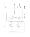
図1は、典型的な同期バックコンバータ10のブロック図である。当該コンバータは、パルス幅調整(PWM)IC16によって操作されるハイ側FET12とロー側FET14を有する。Q1及びQ2デバイス12、14は、プリント回路基板(PCB)上のハイ側FET12のソースをロー側FET14のドレインに接続することによって生じる寄生の抵抗18及びインダクタンス20を減少させるための最適なレイアウトを要する分離したデバイスとして構成され得る。
FIG. 1 is a block diagram of a typical
公開番号2005/0285238A1よって2005年12月29日に公開された発明者Joshi他による米国特許出願には、ロー側ランドとハイ側ランドを明確にするリードフレーム構造を含む集積トランジスタモジュールが開示されている。ロー側トランジスタはロー側ランド上に搭載され、そのドレインは、ロー側ランドに電気的に接続されている。ハイ側トランジスタは、ハイ側ランド上に搭載され、そのソースはハイ側ランドに電気的に接続されている。リードフレーム構造の階段状部分は、ロー及びハイ側のランドに電気的に接続しており、それゆえ、また、ロー側トランジスタのドレインとハイ側トランジスタのソースに接続している。 US patent application by inventor Joshi et al. Published December 29, 2005 by publication number 2005 / 0285238A1 discloses an integrated transistor module including a lead frame structure that defines a low side land and a high side land. Yes. The low-side transistor is mounted on the low-side land, and its drain is electrically connected to the low-side land. The high-side transistor is mounted on the high-side land, and its source is electrically connected to the high-side land. The stepped portion of the lead frame structure is electrically connected to the low and high side lands and is therefore also connected to the drain of the low side transistor and the source of the high side transistor.
後述の特許公開公報の集積トランジスタモジュールは意図された用途には有用であるが、モジュールのフットプリントは産業界において共通でない。 The integrated transistor modules of the patent publications described below are useful for their intended use, but the module footprint is not common in the industry.
それゆえ、これらの問題の解決法を提供する同期バックコンバータ回路のような回路で用いることができる改良された集積電力デバイスモジュールが必要である。 Therefore, there is a need for an improved integrated power device module that can be used in circuits such as synchronous buck converter circuits that provide a solution to these problems.
本願発明によれば、これらの問題の解決法が提供される。 The present invention provides a solution to these problems.
本願発明の一態様によれば、互いに離間した第1及び第2のパッドと、前記第1及び第2のパッドの間に配置された1つ以上の共通ソース−ドレインリードと、を有するリードフレーム構造と、前記第1及び第2のパッドにそれぞれフリップチップ取り付けされている第1及び第2のトランジスタと、前記第1のトランジスタのドレインに取り付けられ且つ前記1つ以上の共通ソース−ドレインリードに電気的に接続されている第1のクリップと、を含み、前記第2のトランジスタのソースが前記1つ以上の共通ソース−ドレインリードに電気的に接続されている集積電力デバイスモジュールが提供される。 According to one aspect of the present invention, a lead frame having first and second pads spaced apart from each other, and one or more common source-drain leads disposed between the first and second pads. A structure, first and second transistors flip-chip attached to the first and second pads, respectively, and attached to a drain of the first transistor and to the one or more common source-drain leads. An integrated power device module comprising: a first clip electrically connected; wherein a source of the second transistor is electrically connected to the one or more common source-drain leads. .
本願発明の別の一態様によれば、互いに離間した第1及び第2のパッドと、前記第1及び第2のパッドの間に配置された1つ以上の共通ソース−ドレインリードと、前記第2のパッドの外側に配置された1つ以上のドレインリードと、を有するリードフレーム構造と、記第1及び第2のパッドにフリップチップ取り付けされている第1及び第2のトランジスタと、前記第1のトランジスタのドレインに取り付けられ且つ前記1つ以上の共通ソース−ドレインリードに電気的に接続されている第1のクリップと、前記第2のトランジスタのドレインに取り付けられ、且つ前記第2のパッドの外側に配置された前記1つ以上のドレインリードに電気的に接続されている第2のクリップと、前記リードフレーム構造、前記トランジスタ及び前記クリップを包埋するモールド材と、を含んで前記モジュールを形成し、前記第2のトランジスタのソースが前記1つ以上の共通ソース−ドレインリードに電気的に接続されている集積電力デバイスモジュールが提供される。 According to another aspect of the present invention, the first and second pads spaced apart from each other, one or more common source-drain leads disposed between the first and second pads, and the first A lead frame structure having one or more drain leads disposed outside the two pads; first and second transistors flip-chip attached to the first and second pads; A first clip attached to a drain of one transistor and electrically connected to the one or more common source-drain leads; and attached to a drain of the second transistor and the second pad A second clip electrically connected to the one or more drain leads disposed outside the lead frame structure, the transistor, and the clip. An integrated power device module comprising: a mold material that embeds the substrate; and forming the module, wherein a source of the second transistor is electrically connected to the one or more common source-drain leads. Is done.
本願発明の別の一態様によれば、互いに離間した第1及び第2のパッドと、前記第1及び第2のパッドの間に配置される1つ以上の共通ソース−ドレインリードと、前記第2のパッドの外側に配置される1つ以上のドレインリードと、を有するリードフレーム構造を提供するステップと、第1及び第2のトランジスタをそれぞれ前記第1及び第2のパッドにフリップチップ取り付けるフリップチップ取り付けステップと、第1のクリップを前記第1のトランジスタのドレインに取り付け、前記第1のクリップを前記1つ以上の共通ソース−ドレインリードに電気的に接続するステップと、第2のクリップを前記第2のトランジスタのドレインに取り付け、前記第2のクリップを前記第2のパッドの外側に配置された前記1つ以上のドレインリードに電気的に接続するステップと、前記リードフレーム構造、前記トランジスタ及び前記クリップをモールド材で包埋して前記モジュールを形成するステップと、を含み、前記フリップチップ取り付けステップにおいて、前記第2のトランジスタのソースを前記1つ以上の共通ソース−ドレインリードに電気的に接続する集積電力デバイスモジュールの製造方法が提供される。 According to another aspect of the present invention, the first and second pads spaced apart from each other, one or more common source-drain leads disposed between the first and second pads, and the first Providing a lead frame structure having one or more drain leads disposed outside the two pads, and flip-chip attaching the first and second transistors to the first and second pads, respectively. Attaching a chip; attaching a first clip to a drain of the first transistor; electrically connecting the first clip to the one or more common source-drain leads; and a second clip The one or more drain reservoirs attached to the drain of the second transistor and having the second clip disposed outside the second pad. A step of electrically connecting the lead frame structure, the transistor and the clip with a molding material to form the module, wherein in the flip chip mounting step, the second step A method of manufacturing an integrated power device module is provided that electrically connects a source of a transistor to the one or more common source-drain leads.
本願発明の別の一態様によれば、熱クリップの露出された上部に対して実質的に垂直である複数の屈曲部を備える露出された上部熱クリップと、露出された熱リードフレーム構造パッドとを有する部分的に包埋された半導体パッケージが提供される。 According to another aspect of the present invention, an exposed upper thermal clip comprising a plurality of bends that are substantially perpendicular to the exposed upper portion of the thermal clip, and an exposed thermal leadframe structure pad. A partially embedded semiconductor package is provided.
本願発明の別の一態様によれば、制御セグメント、第1高電流セグメント及び第2高電流セグメントの3つの分離したセグメントを有する共面リードフレーム構造を提供し、半導体デバイスを制御セグメントと第1電流セグメントの2つに取り付け、クリップを複数の屈曲部を有するリードフレーム構造の反対側の半導体デバイスの片側に取り付け、その複数の屈曲部は第2電流セグメントに取り付けられ、モールド材を用いてリードフレーム構造、半導体デバイス及びクリップを部分的に包埋してパッケージを形成する部分的に包埋された半導体パッケージの製造方法が提供される。 According to another aspect of the present invention, a coplanar leadframe structure having three separate segments, a control segment, a first high current segment, and a second high current segment, is provided, the semiconductor device being connected to the control segment and the first segment. Attached to two of the current segments, the clip is attached to one side of the semiconductor device on the opposite side of the lead frame structure having a plurality of bends, the plurality of bends being attached to the second current segment, and using a molding material A method of manufacturing a partially embedded semiconductor package is provided in which a frame structure, a semiconductor device and a clip are partially embedded to form a package.
前述の及び他の態様、特性、利点、及び発明は、一般に、添付図面に関連してなされる以下のより詳細な説明から、より良く理解される。 The foregoing and other aspects, features, advantages, and inventions will be better understood from the following more detailed description, generally taken in conjunction with the accompanying drawings.
明確さ及び適当と考えられる目的のため、参照数字は、対応するものを示すために図面において繰り返えされると認められる。また、図面における様々な対象の相対的な寸法は、幾つかの場合においては、発明をより明確に示すために変更されている。 For purposes of clarity and appropriateness, it will be appreciated that reference numerals will be repeated in the drawings to indicate corresponding things. Also, the relative dimensions of various objects in the drawings have been changed in some cases to more clearly illustrate the invention.
発明の実施例は、半導体ダイパッケージと半導体ダイパッケージの製造方法を対象としたものである。発明の実施例による半導体ダイパッケージは、基板と、基板上に搭載された半導体ダイと、を含む。半導体ダイは、接着剤又は他の好適な付着材を用いて基板に取り付けられても良い。半導体ダイパッケージにおいては、半導体ダイの下表面及び/又は上表面は、基板の導電領域に電気的に結合されても良い。モールド材が半導体ダイを包埋しても良い。以下に、より詳細に説明されるように、発明の複数の実施例による基板は、異なる実施例における異なる構成とすることができる。 Embodiments of the invention are directed to semiconductor die packages and methods for manufacturing semiconductor die packages. A semiconductor die package according to an embodiment of the invention includes a substrate and a semiconductor die mounted on the substrate. The semiconductor die may be attached to the substrate using an adhesive or other suitable adhesive. In a semiconductor die package, the lower surface and / or the upper surface of the semiconductor die may be electrically coupled to a conductive region of the substrate. The mold material may embed the semiconductor die. As will be described in more detail below, substrates according to embodiments of the invention may be configured differently in different embodiments.
基板はいくつかの好適な構成を有する。しかしながら、発明の好ましい実施例においては、基板はリードフレーム構造とモールド材とを含む。典型的には、リードフレーム構造の少なくとも1つの表面が、モールド材の外側の表面とほぼ共面になっている。幾つかの実施例においては、リードフレーム構造の対向する主表面の両方が、基板におけるモールド材の対向する外側の表面とほぼ共面になっている。 The substrate has several suitable configurations. However, in a preferred embodiment of the invention, the substrate includes a lead frame structure and a mold material. Typically, at least one surface of the lead frame structure is substantially coplanar with the outer surface of the mold material. In some embodiments, both opposing major surfaces of the leadframe structure are substantially coplanar with the opposing outer surfaces of the mold material on the substrate.
用語「リードフレーム構造」とは、リードフレームに由来する構造ということができる。リードフレーム構造は、例えば当該技術分野で知られているスタンピング工程によって形成される。典型的なリードフレーム構造は、また、所定のパターンを形成するための連続的な導電シートをエッチングすることによって形成され得る。それゆえ、発明の実施例においては、半導体ダイパッケージ内のリードフレーム構造は、連続的な金属の構造又は不連続的な金属の構造としても良い。 The term “lead frame structure” may be referred to as a structure derived from a lead frame. The lead frame structure is formed by, for example, a stamping process known in the art. A typical leadframe structure can also be formed by etching a continuous conductive sheet to form a predetermined pattern. Therefore, in an embodiment of the invention, the lead frame structure in the semiconductor die package may be a continuous metal structure or a discontinuous metal structure.
発明の実施例によるリードフレーム構造は、最初は、連結バーによって一体に接続されたリードフレーム構造の配置における多くのリードフレーム構造のうちの1つであっても良い。半導体ダイパッケージの製造工程中で、リードフレーム構造配置は、互いに分離独立したリードフレーム構造に切断されても良い。この切断の結果として、最終的な半導体ダイパッケージにおけるリードフレーム構造(例えばソースリードやゲートリード)は、電気的に又は機械的に互いに結合しないようにしても良い。別の実施例においては、リードフレーム構造の配置は、発明の実施例による半導体ダイパッケージの製造をするときには用いられない。 The lead frame structure according to an embodiment of the invention may initially be one of many lead frame structures in an arrangement of lead frame structures connected together by a connecting bar. During the manufacturing process of the semiconductor die package, the lead frame structure arrangement may be cut into lead frame structures that are separated from each other. As a result of this cutting, the lead frame structure (eg, source lead or gate lead) in the final semiconductor die package may not be electrically or mechanically coupled to each other. In another embodiment, the lead frame structure arrangement is not used when manufacturing a semiconductor die package according to an embodiment of the invention.
発明の実施例によるリードフレーム構造は、好適な材料からなり、好適な形状を有し、好適な厚さを有するようにしても良い。典型的なリードフレーム構造材は、例えば銅、アルミニウム、金などの金属を含む。リードフレーム構造は、また、例えば金、クロム、銀、パラジウム、ニッケルなどのめっき層を含む。 Leadframe structures according to embodiments of the invention may be made of a suitable material, have a suitable shape, and have a suitable thickness. Typical leadframe structural materials include metals such as copper, aluminum, and gold. The lead frame structure also includes a plating layer such as gold, chromium, silver, palladium, nickel, and the like.
発明の実施例による半導体ダイパッケージは、また、いくつかの好適な構成を有する。例えば、リードフレーム構造は、また、約1mmよりも小さい(例えば約0.5mmよりも小さい)厚さを含むいくつかの好適な厚さを有する。更に、リードフレーム構造は、ダイ取り付けパッド(DAP)を形成し得るダイ取り付け領域を有しても良い。リードは、ダイ取り付け領域から遠ざかるように横に伸びても良い。それらは、また、ダイ取り付け領域を形成する表面と共面をなす表面を有しても良い。 The semiconductor die package according to the embodiments of the invention also has several suitable configurations. For example, the lead frame structure also has a number of suitable thicknesses including a thickness of less than about 1 mm (eg, less than about 0.5 mm). Further, the lead frame structure may have a die attach area that can form a die attach pad (DAP). The lead may extend laterally away from the die attach area. They may also have a surface that is coplanar with the surface forming the die attach area.
基板に用いられるモールド材は好適な材料からなる。好適なモールド材は、ビフェニールを基礎とした材料と、多機能架橋エポキシ樹脂合成材料とを含む。好適なモールド材は、リードフレーム構造上に液状又は半固体状で堆積され、その後、それらを固めるための対策が施される。 The molding material used for the substrate is made of a suitable material. Suitable mold materials include biphenyl based materials and multifunctional cross-linked epoxy resin composite materials. Suitable mold materials are deposited in liquid or semi-solid form on the lead frame structure and then measures are taken to harden them.
基板上に搭載された半導体ダイは、いくつかの好適な半導体デバイスを含んでも良い。好適なデバイスは垂直なデバイスを含む。垂直なデバイスは、電流がダイを通じて垂直に流れるように、少なくとも、ダイの一方の側に入力を、ダイの他方の側に出力を有する。典型的な半導体デバイスは、また、2004年12月29日に提出された米国特許出願番号11/026,276に記載されており、当該出願は、全ての目的のためにその全体を参照することによって、ここに取り入れられる。 A semiconductor die mounted on a substrate may include a number of suitable semiconductor devices. Suitable devices include vertical devices. A vertical device has at least an input on one side of the die and an output on the other side of the die so that current flows vertically through the die. A typical semiconductor device is also described in US patent application Ser. No. 11 / 026,276, filed Dec. 29, 2004, which is hereby incorporated by reference in its entirety for all purposes. Is incorporated here.
垂直電力トランジスタは、VDMOSトランジスタと垂直バイポーラトランジスタとを含む。VDMOSトランジスタは、拡散によって形成された2つ又はそれ以上の半導体領域を有するMOSFETである。それは、ソース領域、ドレイン領域及びゲートを有する。そのデバイスは垂直であり、ソース領域とドレイン領域とが半導体ダイの対向する表面にある。ゲートは、トレンチゲート構造又はプラナーゲート構造であり、ソース領域と同じ表面に形成される。トレンチゲート構造はプラナーゲート構造に比較して狭く、占める空間が小さいので、トレンチゲート構造が望ましい。動作中、VDMOSデバイスにおけるソース領域からドレイン領域への電流の流れは、ダイ表面に対してほぼ垂直である。 The vertical power transistor includes a VDMOS transistor and a vertical bipolar transistor. A VDMOS transistor is a MOSFET having two or more semiconductor regions formed by diffusion. It has a source region, a drain region and a gate. The device is vertical and the source and drain regions are on opposite surfaces of the semiconductor die. The gate has a trench gate structure or a planar gate structure and is formed on the same surface as the source region. The trench gate structure is desirable because the trench gate structure is narrower and occupies less space than the planar gate structure. In operation, the current flow from the source region to the drain region in the VDMOS device is substantially perpendicular to the die surface.
モールド材は、半導体ダイを包埋するために用いられる。モールド材は、上記のモールド材と同一又は異なる種類の材料からなるものでも良い。いくつかの実施例においては、モールド材が、少なくとも部分的に、基板と、基板上の1つ以上の半導体ダイスを覆う。モールド材は、周辺環境にさらされることによる潜在的な損傷から1つ以上の半導体ダイを保護するのに用いられる。 The mold material is used to embed a semiconductor die. The mold material may be made of the same or different kind of material as the mold material. In some embodiments, the molding material at least partially covers the substrate and one or more semiconductor dies on the substrate. The mold material is used to protect one or more semiconductor dies from potential damage from exposure to the surrounding environment.
いくつかの好適な工程が、1つ又は複数の半導体ダイ及び/又は1つ又は複数の半導体ダイスを支持する基板を包埋するのに用いられる。例えば、半導体ダイと基板がモールディングダイに置かれても良く、モールド材が半導体ダイ及び/又は基板の少なくとも一部の周囲に形成されても良い。明確なモールディング状態は、当該技術分野における通常の知識を有する者に知られている。 Several suitable processes are used to embed one or more semiconductor dies and / or a substrate that supports one or more semiconductor dies. For example, the semiconductor die and the substrate may be placed on the molding die, and the molding material may be formed around at least a part of the semiconductor die and / or the substrate. Clear molding conditions are known to those with ordinary knowledge in the art.
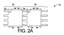
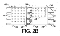
図2Aは、本願発明の一実施例による両側冷却集積電力デバイスモジュールを形成するのに用いられる種類の2つのリードフレーム構造32及び34の平面図30である。リードフレーム構造32及び34は、図2A−2Cに示される接続バー36を有する。接続バー36は、包埋処理の後の個別化工程において取除かれるものであり、図を雑然とさせるのを避けるために他の図には示されていない。接続バーは、リードフレーム構造32及び34を1群として配置し且つ1つのリール内に組み立てられるようにするものである。図2Bに示されるように、半田ペースト38は、2つのクリップ40及び42に半田付けされるリードフレーム構造32及び34のリードに用いられる。2つの電力デバイス44及び46は、裏返しにされ、それぞれリードフレーム構造32及び34上に配置される。電力デバイス44及び46は、チップの製造中に半田によって覆われる。図2Cにおける2つのクリップ40及び42は、それぞれ、リードフレーム構造32及び34と電力デバイス44及び46を覆うように配置されている。モジュールは、電力デバイス44及び46をリードフレーム構造32及び34に接合するため、及びリードフレーム構造32及び34の適当なリード上及び電力デバイス44及び46の後ろ側のそれぞれに半田ペーストをリフローするために加熱される。本願発明は、複数のMOSFET又は単独のMOSFETに限定されないが、議論を簡単にするために、電力デバイス44及び46は、以下、MOSFET44及び46として参照される。例えば、FET12及び14のソース及びドレインを横切るダイオードは、電力デバイス44及び46の部分でも良い。
FIG. 2A is a
図2Bに見られるように、リード48及び50は、それぞれ、MOSFET44及び46のそれぞれのゲートに接続されている。これらのリードは、個別化工程後、リードフレーム構造32及び34のそれぞれの残余から電気的に分離される。リード48及び50に接続されていないリードフレーム構造32及び34の部分は、それぞれ、MOSFET44及び46のソースに接続されている。MOSFET44及び46のドレインは、それぞれクリップ40及び42に半田付けされている。
As seen in FIG. 2B, leads 48 and 50 are connected to respective gates of
クリップ40及び42は、平面部材52と、リフロー半田付け工程中に半田ペースト38でリードに半田付けされた複数の下方に伸長したリード54とを有する。その結果、MOSFET44のソースは、クリップ40によりMOSFET46のドレインに接続される。
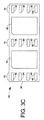
図3A、3B及び3Cは、例えばエポキシのようなモールド材68で部分的に包埋された、図2Cに示される構造である集積電力デバイスモジュール66の、それぞれ上面図60、断面側面図62及び底面図64である。断面図3Bは、図3Aにおける線3B−3Bに沿ったものである。平面部材52は、図3Aにおけるモジュール66の上部において露出されている。図3Cに示されるように、モジュール66の底部は、リードフレーム構造32及び34の部分である露出されたソースパッド78及び80に沿って、リードランド72、74及び76の列を有する。リード82、84及び86は、ソースパッド78であるMOSFET44のソースに接続されている。リード88、90及び92は、MOSFET44のドレインとMOSFET46のソースの共通接続部であり、リード94、96、98及び100は、クリップ42によってMOSFET46のエミッタに接続されている。
FIGS. 3A, 3B, and 3C show a
モジュール66は、2つの別個のFET12及び14を、FET12がMOSFET44によって置き換えられ且つFET14がMOSFET46によって置き換えられたモジュール66に置き換えることによって、図1の同期バックコンバータ10に用いるのに適当となるものである。モジュール66を用いることによって、低い側のMOSFET44のドレインの、高い側のMOSFET46のソースへの電気的な接続を提供するクリップ40を有し、2つのMOSFET44及び46は共に物理的により近づき、寄生の抵抗18及びインダクタンス20は実質的に低減される。その上、電力FETの冷却は、上表面56が包埋されていないクリップ40及び42の固有の熱効果特性によって改善されている。2つのデバイスのソースが、それらが取り付けられているリードフレーム構造を経由して露出されているので、冷却は両側冷却によってより改善されている。単一の半田リフローが、複合の半田リフローよりも要望されているので、モジュール66の製造方法は、また、半田接合の信頼性を向上させる。
図4A、4B及び4Cは、本願発明の別の実施例による両側冷却集積電力デバイスモジュール102の底面図及び側面断面図である。底面図4Aは、ソースパッド114及び116に沿った、リードランド106、108、110及び112の4つの列を示している。モジュール102が製造されたときには、列108及び110のリードは、図4B及び4Cに示されるように一体に接続されている。しかし、それらは、図4B及び4Cに示される線118に沿ってモジュール102を切断することによって、モジュール102が2つの分離した単一の電力デバイスモジュールに分割され、列108のリードが列110のリードから分離するように設計されている。断面図4B及び4Cは、それぞれ図4Aの線4B−4B及び4C−4Cに沿って得られたものである。図4Cでは、リードランド120、122及び124は、MOSFET36及び38のためのゲートランドである。モジュール102が線118に沿って分割された場合には、リードランド122は分離される。
4A, 4B, and 4C are a bottom view and a side cross-sectional view of a double-sided cooled integrated
図5は、本願発明の別の実施例による、リードが設けられた両側冷却集積電力デバイスモジュール140の断面図である。モジュール140は、ランドパッド144と一体化された外部リード142をモジュール140の端部に有する。ランドパッド144は、先の実施例のようにモジュール140の底部において露出されているが、モジュール140の底面の上のモジュール140の端部に存在する第1の水平部146へ向かって上ることによってモールド材の外に伸長しており、それからモジュール140の底面におおよそ整列している第2の水平部148へ向かって下っている。このリードが設けられたモジュール140は、したがって、リードパッケージフットプリントを収容することができる。外部リード142は、線150及び152でモジュール140の端部を切断することによりリードレスモジュールを形成するために除去されても良い。
FIG. 5 is a cross-sectional view of a double-sided cooled integrated power device module 140 provided with leads according to another embodiment of the present invention. The module 140 has
図6A及び6Bは、本願発明の別の実施例による両側冷却集積電力デバイスモジュール164を形成するための図4Cに示されるモジュールの変形のそれぞれの断面側面図160及び162である。2つのMOSFET36及び38のドレインは、共通ドレインを形成するために一体に接続されている。図6Aにおいては、MOSFET36及び38を分離するためにリードフレーム構造168にスワンカット166が形成されている。図6Bにおいては、電気的及び熱的伝導ヒートシンク170が、共通ドレイン接続を形成するためのクリップ44及び46の平面部材54に取り付けられている。
6A and 6B are cross-sectional
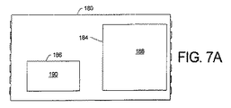
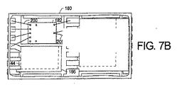
図7A、7B及び7Cは、本願発明の別の実施例による両側冷却集積電力デバイスモジュール180のそれぞれ上面図、部分断面上面図、底面図である。当該実施例は、それぞれカスタマイズされたクリップ184及び186を有する2つのMOSFET44及び46を操作するため、MOSFET44のドレインをMOSFET46のソースに接続するため、及びMOSFET44及び46のための冷却を提供するための制御IC182を含む。図7Aは、モジュール180の上部において露出されたクリップ184及び186の平面部材188及び190の各々を表す上面図である。図7Cに示されるように、モジュール180は、モールド材198の端部を越えて伸長している端部リードランドと共に、リードランド192、194及び196の3つの列を有する。図7Bは、モジュール180の部分断面の上面図である。制御IC182は、列192における幾つかのリードランドへの、及びMOSFET46のゲート及びソースへの、複数のワイヤボンド200を有する。クリップ184及び186の形態、及びモジュール180のフットプリントは、本願発明の柔軟性を説明する先に記載されたモジュールとは異なる。
7A, 7B and 7C are a top view, a partial cross-sectional top view and a bottom view, respectively, of a double side cooled integrated
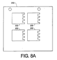
図8Aは、本願発明の実施例の1つの用途のために、良く知られた操作方法を用いて金属フレームから穴開けされる4つのクリップ202の輪郭を示す金属板200の上面図である。このように、クリップ202は、集合して配置され且つ1つのリールで作製され得る。図8Bは、図8Aに示される金属板から押し出され、図3Bで用いられたクリップに成形された後の2つのクリップ202の側面図である。図8Bに示されるように、クリップ202は、半田付けの向上のためにそれらに形成された溝204を有する。
FIG. 8A is a top view of the
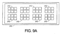
図9Aは、複数の部分的に包埋されたモジュール212のブロックモールド210の上面図である。図5に示されるリードが設けられたモジュール140の事例のモールドの場合、モジュール140は、個別化されたモジュールとして形成される。図9Bは、ブロックモールド210から個別化された後の図3A−3Cに示される包埋されたモジュール66の種類の底面図である。いずれのリードレスモジュールもブロックモールド210内に形成され得ると認められる。
FIG. 9A is a top view of a
図10は、本願発明の別の実施例による電力半導体パッケージ300の等角部分断面図である。パッケージ300は、3つの分離セグメント、つまり、制御セグメントすなわちゲートセグメント302、第1電流キャリーセグメントすなわちソースセグメント304、及び第2電流キャリーセグメントすなわちドレインセグメント306からなるリードフレーム構造を有する。ゲートセグメント302は、モールド材310を越えて伸長する外部リード308を含み且つゲートセグメント302のより厚い部分312の部分である。垂直表面314は、ゲートセグメント302のより厚い部分312の部分とより薄い部分316との間の境界を明示している。
FIG. 10 is an isometric partial cross-sectional view of a
ソースセグメント304は、ソースセグメント304の3つのより厚い部分320の部分であり且つモールド材310を越えて伸長する3つの外部リード318を有する。垂直表面322は、ソースセグメント304のより厚い部分320とより薄い部分324との間の境界を明示している。より薄い部分324は、実質的に下方に横たわっているソースセグメント304の本体の部分であり、半導体デバイス326に取り付けられている。別のより厚い部分328は、ソースセグメント304の本体の部分の下に伸長している。ソースセグメント304は、半導体パッケージ300が組み立てられるときに適所にあってソースセグメントを保持するのに用いられる2つの連結バー330及び332(図11に示される)を有する。
ドレインセグメント306は、ドレインセグメント306の4つのより厚い部分336の部分であり且つモールド材310を越えて伸長する4つの外部リード334を有する。垂直表面338は、ドレインセグメント306のより厚い部分336とより薄い部分340との間の境界を明示している。
半導体デバイス326は、ソースセグメント304だけでなくゲートセグメント302にも取り付けられている。半導体デバイスは、半田バンプ342及び半田344によってゲートセグメント302にそのゲートが取り付けられ且つ半田バンプ346及び半田344によってソースセグメント304にそのソースが取り付けられたフリップチップパワーMOSFETでも良い。なお、それらの全てが図10に示されているわけではない。
The
半導体デバイス300の上部への取り付けは、上表面352と各々が分岐端356を有する3つの屈曲部354とを有するドレインクリップ350であり得るスタッド又はクリップ350によってなされる。分岐部356は、半田344によってエミッタセグメント306に取り付けられる。分岐部356の各々は、半導体デバイス326上の半田バンプの形状に似せて形作られた丸み部360(図11及び15に示される)に終わる。ドレインクリップ350は、クリップの3つの上端上の中間部に沿った切り取り領域362を形成するためにハーフエッチングされる。切り取り領域362は、モールド材310と共にドレインクリップ350を適所にしっかり固定するのを助ける。モールド材310は、ドレインクリップ350の上表面352及びゲートセグメント302のより厚い部分312、ソースセグメント304のより厚い部分320及び328、及びドレインセグメント306のより厚い部分336を露出させつつ、パッケージ300の上部から底部へ伸長している。
Attachment to the top of the
図11は、図10に示される電力半導体パッケージ300の分解図であり、モールド材310を除いて残存しているパッケージ300の構成要素の全体図を提供している。
FIG. 11 is an exploded view of the
図12は、パッケージ300の個別化に先立ってリードフレームの部分372に接続されたリードフレーム構造セグメント302、304及び306と共に輪郭で示されるモールド材310と共に、半導体パッケージ300を示す上面図370である。図12に示されるように、エミッタセグメント306のより厚い部分336とより薄い部分340との間の直角エッジ338は、外部リード334の端部に対して平行になっているだけでなく、図12において伸長している。切断線374は、パッケージ300が個別化された後における外部リード308、318及び334の端部の位置を示す。
FIG. 12 is a
図13及び14は、図10に示される半導体パッケージ300のそれぞれ等角上面図及び等角底面図である。図14に示されるように、リードフレーム構造のゲートセグメント302、ソースセグメント304及びエミッタセグメント306のより厚い部分は、パッケージ300の底部において露出されている。一方、3つのセグメント302、304及び306のより薄いセグメントはモールド材310内に包まれている。ソースセグメント304のより厚い部分328の露出された表面は、ドレインリード318に接続されており、MOSFET326のソースへの電気的な接続のためのドレインリード318に代えて又は加えて用いられても良い。露出された表面380は、また、半導体ダイ326から離れる方向への付加的な熱導電を提供するためにプリント回路基板(PCB)上の金属島に半田付けされても良い。
13 and 14 are an isometric top view and an isometric bottom view, respectively, of the
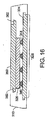
図15は、図13に示される線15−15に沿って得られた第1の図式的断面図である。 FIG. 15 is a first schematic cross-sectional view taken along line 15-15 shown in FIG.
図16は、図13に示される線16−16に沿って得られた第2の図式的断面図である。 FIG. 16 is a second schematic cross-sectional view taken along line 16-16 shown in FIG.
図17は、輪郭で表されるモールド材310を伴う、図10に示される半導体パッケージ300の等角上面図である。
FIG. 17 is an isometric top view of the
図18は、輪郭で表されるモールド材310を伴う、図10に示される半導体パッケージ300の等角底面図である。
18 is an isometric bottom view of the
図19A、19B、19C、19D、19E、19F、19G、19H、19I、19J、19K及び19Lは、パッケージ300の組み立ての様々な段階における図10に示される半導体パッケージ300の等角図である。図19Aは、クリップ350の底を表す。単一のクリップ350のみが表されているものの、クリップ350は、組立工程の当該部分を通じて別のクリップ350に取り付けられていると理解される。半導体ダイ326は、クリップ350上に軟ろうを置き、軟ろう上の適所に半導体ダイ326を置き、半導体ダイ326とクリップ350との間に半田接合を形成するために半田をリフローすることによって、その背面をクリップ350に向けて半田付けされる。
19A, 19B, 19C, 19D, 19E, 19F, 19G, 19H, 19I, 19J, 19K and 19L are isometric views of the
次に、銅バンプ又はウエハレベルボールドロップが、図19Cに示されるように半田バンプ342及び246を形成するために半導体ダイの上面に置かれる。図19Dにおいて、クリップ510は、自身に取り付けられた他のクリップから分離又は個別化される。 A copper bump or wafer level ball drop is then placed on the top surface of the semiconductor die to form solder bumps 342 and 246 as shown in FIG. 19C. In FIG. 19D, clip 510 is separated or individualized from other clips attached to it.
図19Eは、半田ペーストが部分372上に置かれた後における、図12に示されるリードフレームの部分372を示す。図19Dに示される組み立て物は、部分372を覆うように置かれ、図19Fに示される組み立て物を形成するための半田ペーストをリフローすることによって部分372に半田付けされる。半田ペーストをリフローするために必要とされる熱量は、図19Bに示されるクリップ350上に置かれた軟ろうを軟化させるのに必要とされる熱量よりも少ない。それゆえ、クリップ350と半導体ダイ326との間の接合は不安定にならない。
FIG. 19E shows the
次に、モールド材310は、図19Gに示されるようなフィルム補助モールディングを用いて、図19Fに示される組み立て物の上にモールドされる。この組み立て物は、それから、ウエハジェットデフラッシュ(図19H)及びレーザーマーキング(図19I)を受ける。
Next, the
パッケージ300は、それから、図19Jに示される組み立て物を形成するためにリードフレームから個別化される。組み立て物は、それから、検査され(図19K)、梱包され積荷される(図19L)。
本願発明は、ある好ましい実施例との特定の関係において詳細に記述されたが、本願発明の精神及び範囲内において変形及び変更がもたらされると理解される。 Although the present invention has been described in detail with particular reference to certain preferred embodiments, it will be understood that variations and modifications can be effected within the spirit and scope of the invention.
Claims (24)
互いに離間した第1及び第2のパッドと、前記第1及び第2のパッドの間に配置された1つ以上の共通ソース−ドレインリードと、を有するリードフレーム構造と、
前記第1及び第2のパッドにそれぞれフリップチップ取り付けされている第1及び第2のトランジスタと、
前記第1のトランジスタのドレインに取り付けられ且つ前記1つ以上の共通ソース−ドレインリードに電気的に接続されている第1のクリップと、を含み、
前記第2のトランジスタのソースが前記1つ以上の共通ソース−ドレインリードに電気的に接続されていることを特徴とする集積電力デバイスモジュール。 An integrated power device module comprising:
A lead frame structure having first and second pads spaced apart from each other, and one or more common source-drain leads disposed between the first and second pads;
First and second transistors flip-chip attached to the first and second pads, respectively;
A first clip attached to a drain of the first transistor and electrically connected to the one or more common source-drain leads;
An integrated power device module, wherein the source of the second transistor is electrically connected to the one or more common source-drain leads.
互いに離間した第1及び第2のパッドと、前記第1及び第2のパッドの間に配置された1つ以上の共通ソース−ドレインリードと、前記第2のパッドの外側に配置された1つ以上のドレインリードと、を有するリードフレーム構造と、
前記第1及び第2のパッドにフリップチップ取り付けされている第1及び第2のトランジスタと、
前記第1のトランジスタのドレインに取り付けられ且つ前記1つ以上の共通ソース−ドレインリードに電気的に接続されている第1のクリップと、
前記第2のトランジスタのドレインに取り付けられ、且つ前記第2のパッドの外側に配置された前記1つ以上のドレインリードに電気的に接続されている第2のクリップと、
前記リードフレーム構造、前記トランジスタ及び前記クリップを包埋するモールド材と、を含んで前記モジュールを形成し、
前記第2のトランジスタのソースが前記1つ以上の共通ソース−ドレインリードに電気的に接続されていることを特徴とする集積電力デバイスモジュール。 An integrated power device module comprising:
First and second pads spaced apart from each other, one or more common source-drain leads disposed between the first and second pads, and one disposed outside the second pad A lead frame structure having the above drain lead;
First and second transistors flip-chip attached to the first and second pads;
A first clip attached to a drain of the first transistor and electrically connected to the one or more common source-drain leads;
A second clip attached to the drain of the second transistor and electrically connected to the one or more drain leads disposed outside the second pad;
Forming the module including the lead frame structure, the transistor and a molding material embedding the clip;
An integrated power device module, wherein the source of the second transistor is electrically connected to the one or more common source-drain leads.
互いに離間した第1及び第2のパッドを有するリードフレーム構造と、前記第1及び第2のパッドの間に配置される1つ以上の共通ソース−ドレインリードと、前記第2のパッドの外側に配置される1つ以上のドレインリードと、を提供するステップと、
第1及び第2のトランジスタをそれぞれ前記第1及び第2のパッドにフリップチップ取り付けるフリップチップ取り付けステップと、
第1のクリップを前記第1のトランジスタのドレインに取り付け、前記第1のクリップを前記1つ以上の共通ソース−ドレインリードに電気的に接続するステップと、
第2のクリップを前記第2のトランジスタのドレインに取り付け、前記第2のクリップを前記第2のパッドの外側に配置された前記1つ以上のドレインリードに電気的に接続するステップと、
モールド材で前記リードフレーム構造、前記トランジスタ及び前記クリップを包埋して前記モジュールを形成するステップと、を含み、
前記フリップチップ取り付けステップにおいては、前記第2のトランジスタのソースを前記1つ以上の共通ソース−ドレインリードに電気的に接続することを特徴とする集積電力デバイスモジュールの製造方法。 A method for manufacturing an integrated power device module, comprising:
A lead frame structure having first and second pads spaced apart from each other, one or more common source-drain leads disposed between the first and second pads, and outside the second pad. Providing one or more drain leads to be disposed;
A flip chip attaching step for flip chip attaching the first and second transistors to the first and second pads, respectively;
Attaching a first clip to the drain of the first transistor and electrically connecting the first clip to the one or more common source-drain leads;
Attaching a second clip to the drain of the second transistor, and electrically connecting the second clip to the one or more drain leads disposed outside the second pad;
Embedding the lead frame structure, the transistor and the clip with a molding material to form the module,
In the flip chip mounting step, the source of the second transistor is electrically connected to the one or more common source-drain leads.
制御セグメント、第1高電流セグメント及び第2高電流セグメントの3つの分離したセグメントを有する共面リードフレーム構造を提供するステップと、
半導体デバイスを前記制御セグメントと前記第1高電流セグメントの2つに取り付けるステップと、
クリップを複数の屈曲部を有する前記リードフレーム構造の反対側の半導体デバイスの片側に取り付けて、前記複数の屈曲部を前記第2高電流セグメントに取り付けるステップと、
前記リードフレーム構造、前記半導体デバイス及び前記クリップをモールド材で部分的に包埋して前記パッケージを形成するステップと、を含むことを特徴とする部分的に包埋された半導体パッケージの製造方法。 A method of manufacturing a partially embedded semiconductor package, comprising:
Providing a coplanar leadframe structure having three separate segments: a control segment, a first high current segment and a second high current segment;
Attaching a semiconductor device to two of the control segment and the first high current segment;
Attaching a clip to one side of a semiconductor device opposite the leadframe structure having a plurality of bends, and attaching the plurality of bends to the second high current segment;
Forming the package by partially embedding the lead frame structure, the semiconductor device and the clip with a molding material, and manufacturing the partially embedded semiconductor package.
Applications Claiming Priority (2)
| Application Number | Priority Date | Filing Date | Title |
|---|---|---|---|
| US11/829,793 US7663211B2 (en) | 2006-05-19 | 2007-07-27 | Dual side cooling integrated power device package and module with a clip attached to a leadframe in the package and the module and methods of manufacture |
| PCT/US2008/070611 WO2009017999A2 (en) | 2007-07-27 | 2008-07-21 | Dual side cooling integrated power device package and module and methods of manufacture |
Publications (2)
| Publication Number | Publication Date |
|---|---|
| JP2010534937A true JP2010534937A (en) | 2010-11-11 |
| JP2010534937A5 JP2010534937A5 (en) | 2011-12-15 |
Family
ID=40316927
Family Applications (1)
| Application Number | Title | Priority Date | Filing Date |
|---|---|---|---|
| JP2010518317A Pending JP2010534937A (en) | 2007-07-27 | 2008-07-21 | Double-side cooled integrated power device package, module and manufacturing method |
Country Status (8)
| Country | Link |
|---|---|
| US (1) | US7663211B2 (en) |
| JP (1) | JP2010534937A (en) |
| KR (1) | KR101324905B1 (en) |
| CN (2) | CN107068641A (en) |
| DE (1) | DE112008001657T5 (en) |
| MY (1) | MY149499A (en) |
| TW (1) | TWI450373B (en) |
| WO (1) | WO2009017999A2 (en) |
Families Citing this family (46)
| Publication number | Priority date | Publication date | Assignee | Title |
|---|---|---|---|---|
| US7663211B2 (en) | 2006-05-19 | 2010-02-16 | Fairchild Semiconductor Corporation | Dual side cooling integrated power device package and module with a clip attached to a leadframe in the package and the module and methods of manufacture |
| US7800219B2 (en) * | 2008-01-02 | 2010-09-21 | Fairchild Semiconductor Corporation | High-power semiconductor die packages with integrated heat-sink capability and methods of manufacturing the same |
| US8063472B2 (en) * | 2008-01-28 | 2011-11-22 | Fairchild Semiconductor Corporation | Semiconductor package with stacked dice for a buck converter |
| US8193618B2 (en) * | 2008-12-12 | 2012-06-05 | Fairchild Semiconductor Corporation | Semiconductor die package with clip interconnection |
| US7816784B2 (en) * | 2008-12-17 | 2010-10-19 | Fairchild Semiconductor Corporation | Power quad flat no-lead semiconductor die packages with isolated heat sink for high-voltage, high-power applications, systems using the same, and methods of making the same |
| US8049312B2 (en) * | 2009-01-12 | 2011-11-01 | Texas Instruments Incorporated | Semiconductor device package and method of assembly thereof |
| US8278756B2 (en) * | 2010-02-24 | 2012-10-02 | Inpaq Technology Co., Ltd. | Single chip semiconductor coating structure and manufacturing method thereof |
| TWI427717B (en) * | 2010-12-28 | 2014-02-21 | Alpha & Omega Semiconductor Cayman Ltd | A method of flip chip package |
| US8344464B2 (en) | 2011-05-19 | 2013-01-01 | International Rectifier Corporation | Multi-transistor exposed conductive clip for high power semiconductor packages |
| US9717146B2 (en) | 2012-05-22 | 2017-07-25 | Intersil Americas LLC | Circuit module such as a high-density lead frame array (HDA) power module, and method of making same |
| US8759956B2 (en) * | 2012-07-05 | 2014-06-24 | Infineon Technologies Ag | Chip package and method of manufacturing the same |
| US9478484B2 (en) | 2012-10-19 | 2016-10-25 | Infineon Technologies Austria Ag | Semiconductor packages and methods of formation thereof |
| US8963303B2 (en) | 2013-02-22 | 2015-02-24 | Stmicroelectronics S.R.L. | Power electronic device |
| US9070721B2 (en) | 2013-03-15 | 2015-06-30 | Semiconductor Components Industries, Llc | Semiconductor devices and methods of making the same |
| JP6147588B2 (en) * | 2013-07-01 | 2017-06-14 | ルネサスエレクトロニクス株式会社 | Semiconductor device |
| US9536800B2 (en) | 2013-12-07 | 2017-01-03 | Fairchild Semiconductor Corporation | Packaged semiconductor devices and methods of manufacturing |
| US9355942B2 (en) * | 2014-05-15 | 2016-05-31 | Texas Instruments Incorporated | Gang clips having distributed-function tie bars |
| US9673097B2 (en) | 2015-05-11 | 2017-06-06 | Texas Instruments Incorporated | Integrated clip and lead and method of making a circuit |
| CN106601694B (en) * | 2015-10-16 | 2020-09-15 | 台达电子工业股份有限公司 | Stack structure and manufacturing method thereof |
| US9496208B1 (en) | 2016-02-25 | 2016-11-15 | Texas Instruments Incorporated | Semiconductor device having compliant and crack-arresting interconnect structure |
| DE102016107792B4 (en) | 2016-04-27 | 2022-01-27 | Infineon Technologies Ag | Pack and semi-finished product with a vertical connection between support and bracket and method of making a pack and a batch of packs |
| US10189535B1 (en) * | 2016-10-12 | 2019-01-29 | Arnott T&P Holding, Llc | Motorcycle display unit system and method |
| DE102016220553A1 (en) * | 2016-10-20 | 2018-04-26 | Robert Bosch Gmbh | power module |
| KR102213604B1 (en) | 2017-02-15 | 2021-02-05 | 매그나칩 반도체 유한회사 | Semiconductor Package Device |
| US10121742B2 (en) * | 2017-03-15 | 2018-11-06 | Amkor Technology, Inc. | Method of forming a packaged semiconductor device using ganged conductive connective assembly and structure |
| US10727151B2 (en) * | 2017-05-25 | 2020-07-28 | Infineon Technologies Ag | Semiconductor chip package having a cooling surface and method of manufacturing a semiconductor package |
| KR102153159B1 (en) | 2017-06-12 | 2020-09-08 | 매그나칩 반도체 유한회사 | Multi-Chip Package of Power Semiconductor |
| US10319670B2 (en) | 2017-10-20 | 2019-06-11 | Semiconductor Components Industries, Llc | Package including multiple semiconductor devices |
| KR20190071111A (en) * | 2017-12-14 | 2019-06-24 | 삼성전자주식회사 | An apparatus for x-ray inspection, and a method for manufacturing a semiconductor device using the same |
| US10916931B2 (en) * | 2018-01-15 | 2021-02-09 | Infineon Technologies Ag | Temperature sensing and fault detection for paralleled double-side cooled power modules |
| US10553517B2 (en) | 2018-01-18 | 2020-02-04 | Semiconductor Components Industries, Llc | High power module semiconductor package with multiple submodules |
| US10438877B1 (en) | 2018-03-13 | 2019-10-08 | Semiconductor Components Industries, Llc | Multi-chip packages with stabilized die pads |
| CN108646159B (en) * | 2018-03-14 | 2020-06-16 | 北京工业大学 | Micro welding spot thermoelectric coupling test method |
| US10665525B2 (en) | 2018-05-01 | 2020-05-26 | Semiconductor Components Industries, Llc | Heat transfer for power modules |
| US10991670B2 (en) | 2018-09-28 | 2021-04-27 | Semiconductor Components Industries, Llc | Semiconductor device assemblies including spacer with embedded semiconductor die |
| US11075137B2 (en) | 2018-05-02 | 2021-07-27 | Semiconductor Components Industries, Llc | High power module package structures |
| US10872848B2 (en) * | 2018-10-25 | 2020-12-22 | Infineon Technologies Ag | Semiconductor package with leadframe interconnection structure |
| DE102018130147A1 (en) | 2018-11-28 | 2020-05-28 | Infineon Technologies Ag | SEMICONDUCTOR DEVICE AND METHOD FOR PRODUCING A SEMICONDUCTOR DEVICE |
| IT201800020998A1 (en) | 2018-12-24 | 2020-06-24 | St Microelectronics Srl | Process for manufacturing semiconductor devices and corresponding semiconductor device |
| US11222832B2 (en) | 2019-02-11 | 2022-01-11 | Semiconductor Components Industries, Llc | Power semiconductor device package |
| US11515244B2 (en) | 2019-02-21 | 2022-11-29 | Infineon Technologies Ag | Clip frame assembly, semiconductor package having a lead frame and a clip frame, and method of manufacture |
| US10964628B2 (en) * | 2019-02-21 | 2021-03-30 | Infineon Technologies Ag | Clip frame assembly, semiconductor package having a lead frame and a clip frame, and method of manufacture |
| US11121055B2 (en) * | 2020-01-10 | 2021-09-14 | Semiconductor Components Industries, Llc | Leadframe spacer for double-sided power module |
| DE102020108916A1 (en) * | 2020-03-31 | 2021-09-30 | Infineon Technologies Ag | Package with clip and connector over electronic components |
| DE102020214912A1 (en) | 2020-11-27 | 2022-06-02 | Robert Bosch Gesellschaft mit beschränkter Haftung | Switching device, electrical energy store, device and method for producing a switching device |
| EP4270476A1 (en) * | 2022-04-29 | 2023-11-01 | Infineon Technologies Austria AG | Semiconductor package and method for marking a semiconductor package |
Citations (4)
| Publication number | Priority date | Publication date | Assignee | Title |
|---|---|---|---|---|
| WO2001015230A1 (en) * | 1999-08-25 | 2001-03-01 | Hitachi, Ltd. | Electronic device |
| JP2002076245A (en) * | 2000-09-04 | 2002-03-15 | Sanyo Electric Co Ltd | Circuit device and its manufacturing method |
| JP2002124596A (en) * | 2000-10-18 | 2002-04-26 | Hitachi Ltd | Semiconductor device and production method therefor |
| WO2006058030A2 (en) * | 2004-11-23 | 2006-06-01 | Siliconix Incorporated | Semiconductor package including die interposed between cup-shaped lead frame and lead frame having mesas and valleys |
Family Cites Families (23)
| Publication number | Priority date | Publication date | Assignee | Title |
|---|---|---|---|---|
| US4961106A (en) * | 1987-03-27 | 1990-10-02 | Olin Corporation | Metal packages having improved thermal dissipation |
| US5796159A (en) * | 1995-11-30 | 1998-08-18 | Analog Devices, Inc. | Thermally efficient integrated circuit package |
| JPH09326463A (en) * | 1996-05-09 | 1997-12-16 | Oki Electric Ind Co Ltd | Resin-sealed semiconductor device |
| KR100421033B1 (en) * | 2000-11-22 | 2004-03-04 | 페어차일드코리아반도체 주식회사 | Power package with high thermal transferability |
| US7345342B2 (en) | 2001-01-30 | 2008-03-18 | Fairchild Semiconductor Corporation | Power semiconductor devices and methods of manufacture |
| US6777800B2 (en) * | 2002-09-30 | 2004-08-17 | Fairchild Semiconductor Corporation | Semiconductor die package including drain clip |
| TWI265611B (en) * | 2003-03-11 | 2006-11-01 | Siliconware Precision Industries Co Ltd | Semiconductor package with heatsink |
| US6867481B2 (en) * | 2003-04-11 | 2005-03-15 | Fairchild Semiconductor Corporation | Lead frame structure with aperture or groove for flip chip in a leaded molded package |
| JP2007066922A (en) * | 2003-11-28 | 2007-03-15 | Renesas Technology Corp | Semiconductor integrated circuit device |
| US6917098B1 (en) * | 2003-12-29 | 2005-07-12 | Texas Instruments Incorporated | Three-level leadframe for no-lead packages |
| JP2005217072A (en) * | 2004-01-28 | 2005-08-11 | Renesas Technology Corp | Semiconductor device |
| US7301235B2 (en) * | 2004-06-03 | 2007-11-27 | International Rectifier Corporation | Semiconductor device module with flip chip devices on a common lead frame |
| US7501702B2 (en) * | 2004-06-24 | 2009-03-10 | Fairchild Semiconductor Corporation | Integrated transistor module and method of fabricating same |
| US7622934B2 (en) | 2004-07-23 | 2009-11-24 | Electronic Bio Sciences, Llc | Method and apparatus for sensing a time varying current passing through an ion channel |
| JP2006073655A (en) * | 2004-08-31 | 2006-03-16 | Toshiba Corp | Semiconductor module |
| US7298134B2 (en) | 2004-10-12 | 2007-11-20 | Elster Electricity, Llc | Electrical-energy meter adaptable for optical communication with various external devices |
| US7394150B2 (en) * | 2004-11-23 | 2008-07-01 | Siliconix Incorporated | Semiconductor package including die interposed between cup-shaped lead frame and lead frame having mesas and valleys |
| US7503695B2 (en) * | 2004-12-01 | 2009-03-17 | Anderson Dale A | Device and method for holding open decoy bags |
| US7256479B2 (en) | 2005-01-13 | 2007-08-14 | Fairchild Semiconductor Corporation | Method to manufacture a universal footprint for a package with exposed chip |
| US7476976B2 (en) * | 2005-02-23 | 2009-01-13 | Texas Instruments Incorporated | Flip chip package with advanced electrical and thermal properties for high current designs |
| US7285849B2 (en) * | 2005-11-18 | 2007-10-23 | Fairchild Semiconductor Corporation | Semiconductor die package using leadframe and clip and method of manufacturing |
| TW200739758A (en) * | 2005-12-09 | 2007-10-16 | Fairchild Semiconductor Corporaton | Device and method for assembling a top and bottom exposed packaged semiconductor |
| US7663211B2 (en) | 2006-05-19 | 2010-02-16 | Fairchild Semiconductor Corporation | Dual side cooling integrated power device package and module with a clip attached to a leadframe in the package and the module and methods of manufacture |
-
2007
- 2007-07-27 US US11/829,793 patent/US7663211B2/en active Active
-
2008
- 2008-07-15 TW TW097126810A patent/TWI450373B/en active
- 2008-07-21 CN CN201710166570.1A patent/CN107068641A/en active Pending
- 2008-07-21 DE DE112008001657T patent/DE112008001657T5/en not_active Withdrawn
- 2008-07-21 JP JP2010518317A patent/JP2010534937A/en active Pending
- 2008-07-21 KR KR1020097027384A patent/KR101324905B1/en active IP Right Grant
- 2008-07-21 CN CN200880016686.6A patent/CN101681897B/en not_active Expired - Fee Related
- 2008-07-21 MY MYPI20095511A patent/MY149499A/en unknown
- 2008-07-21 WO PCT/US2008/070611 patent/WO2009017999A2/en active Application Filing
Patent Citations (4)
| Publication number | Priority date | Publication date | Assignee | Title |
|---|---|---|---|---|
| WO2001015230A1 (en) * | 1999-08-25 | 2001-03-01 | Hitachi, Ltd. | Electronic device |
| JP2002076245A (en) * | 2000-09-04 | 2002-03-15 | Sanyo Electric Co Ltd | Circuit device and its manufacturing method |
| JP2002124596A (en) * | 2000-10-18 | 2002-04-26 | Hitachi Ltd | Semiconductor device and production method therefor |
| WO2006058030A2 (en) * | 2004-11-23 | 2006-06-01 | Siliconix Incorporated | Semiconductor package including die interposed between cup-shaped lead frame and lead frame having mesas and valleys |
Also Published As
| Publication number | Publication date |
|---|---|
| DE112008001657T5 (en) | 2010-06-10 |
| WO2009017999A2 (en) | 2009-02-05 |
| CN101681897A (en) | 2010-03-24 |
| KR20100039293A (en) | 2010-04-15 |
| TW200913201A (en) | 2009-03-16 |
| WO2009017999A3 (en) | 2009-04-02 |
| CN101681897B (en) | 2017-04-12 |
| MY149499A (en) | 2013-09-13 |
| US20080023807A1 (en) | 2008-01-31 |
| KR101324905B1 (en) | 2013-11-04 |
| TWI450373B (en) | 2014-08-21 |
| CN107068641A (en) | 2017-08-18 |
| US7663211B2 (en) | 2010-02-16 |
Similar Documents
| Publication | Publication Date | Title |
|---|---|---|
| US7663211B2 (en) | Dual side cooling integrated power device package and module with a clip attached to a leadframe in the package and the module and methods of manufacture | |
| US7618896B2 (en) | Semiconductor die package including multiple dies and a common node structure | |
| US8513059B2 (en) | Pre-molded clip structure | |
| US7777315B2 (en) | Dual side cooling integrated power device module and methods of manufacture | |
| US8278149B2 (en) | Package with multiple dies | |
| US20120181675A1 (en) | Semiconductor die package and method for making the same | |
| US7501702B2 (en) | Integrated transistor module and method of fabricating same | |
| US20130181332A1 (en) | Package leadframe for dual side assembly | |
| TW201005887A (en) | Four mosfet full bridge module | |
| US20090127677A1 (en) | Multi-Terminal Package Assembly For Semiconductor Devices | |
| KR101157305B1 (en) | Dual side cooling integrated transistor module and methodes of manufacture | |
| KR20220007878A (en) | Electronic devices with double-sided cooling | |
| US8198134B2 (en) | Dual side cooling integrated power device module and methods of manufacture |
Legal Events
| Date | Code | Title | Description |
|---|---|---|---|
| A621 | Written request for application examination |
Free format text: JAPANESE INTERMEDIATE CODE: A621 Effective date: 20110622 |
|
| A521 | Request for written amendment filed |
Free format text: JAPANESE INTERMEDIATE CODE: A523 Effective date: 20111027 |
|
| A977 | Report on retrieval |
Free format text: JAPANESE INTERMEDIATE CODE: A971007 Effective date: 20121207 |
|
| A131 | Notification of reasons for refusal |
Free format text: JAPANESE INTERMEDIATE CODE: A131 Effective date: 20121218 |
|
| A02 | Decision of refusal |
Free format text: JAPANESE INTERMEDIATE CODE: A02 Effective date: 20130521 |