JP2010510685A - Optical adhesive composition for LED light source - Google Patents
Optical adhesive composition for LED light source Download PDFInfo
- Publication number
- JP2010510685A JP2010510685A JP2009538443A JP2009538443A JP2010510685A JP 2010510685 A JP2010510685 A JP 2010510685A JP 2009538443 A JP2009538443 A JP 2009538443A JP 2009538443 A JP2009538443 A JP 2009538443A JP 2010510685 A JP2010510685 A JP 2010510685A
- Authority
- JP
- Japan
- Prior art keywords
- light source
- oxide
- led light
- led
- oxide nanoparticles
- Prior art date
- Legal status (The legal status is an assumption and is not a legal conclusion. Google has not performed a legal analysis and makes no representation as to the accuracy of the status listed.)
- Withdrawn
Links
Images


Classifications
-
- H—ELECTRICITY
- H01—ELECTRIC ELEMENTS
- H01L—SEMICONDUCTOR DEVICES NOT COVERED BY CLASS H10
- H01L33/00—Semiconductor devices with at least one potential-jump barrier or surface barrier specially adapted for light emission; Processes or apparatus specially adapted for the manufacture or treatment thereof or of parts thereof; Details thereof
- H01L33/48—Semiconductor devices with at least one potential-jump barrier or surface barrier specially adapted for light emission; Processes or apparatus specially adapted for the manufacture or treatment thereof or of parts thereof; Details thereof characterised by the semiconductor body packages
- H01L33/58—Optical field-shaping elements
-
- F—MECHANICAL ENGINEERING; LIGHTING; HEATING; WEAPONS; BLASTING
- F21—LIGHTING
- F21V—FUNCTIONAL FEATURES OR DETAILS OF LIGHTING DEVICES OR SYSTEMS THEREOF; STRUCTURAL COMBINATIONS OF LIGHTING DEVICES WITH OTHER ARTICLES, NOT OTHERWISE PROVIDED FOR
- F21V7/00—Reflectors for light sources
- F21V7/0091—Reflectors for light sources using total internal reflection
-
- F—MECHANICAL ENGINEERING; LIGHTING; HEATING; WEAPONS; BLASTING
- F21—LIGHTING
- F21Y—INDEXING SCHEME ASSOCIATED WITH SUBCLASSES F21K, F21L, F21S and F21V, RELATING TO THE FORM OR THE KIND OF THE LIGHT SOURCES OR OF THE COLOUR OF THE LIGHT EMITTED
- F21Y2115/00—Light-generating elements of semiconductor light sources
- F21Y2115/10—Light-emitting diodes [LED]
-
- H—ELECTRICITY
- H01—ELECTRIC ELEMENTS
- H01L—SEMICONDUCTOR DEVICES NOT COVERED BY CLASS H10
- H01L2924/00—Indexing scheme for arrangements or methods for connecting or disconnecting semiconductor or solid-state bodies as covered by H01L24/00
- H01L2924/0001—Technical content checked by a classifier
- H01L2924/0002—Not covered by any one of groups H01L24/00, H01L24/00 and H01L2224/00
Landscapes
- Engineering & Computer Science (AREA)
- Microelectronics & Electronic Packaging (AREA)
- General Engineering & Computer Science (AREA)
- Manufacturing & Machinery (AREA)
- Computer Hardware Design (AREA)
- Power Engineering (AREA)
- Led Device Packages (AREA)
- Adhesives Or Adhesive Processes (AREA)
Abstract
光学接着組成物、及び前記組成物を含むLED光源、並びに前記LED光源の製造方法が開示されている。LED光源は、LEDダイと、前記LEDダイに光学的に結合された光学部品と、非晶質オルガノポリシロキサン網状組織を含む接着層と、を備えていてよく、前記オルガノポリシロキサン網状組織は、式:
(R1SiO1.5)n
(前記式中、R1は有機基であり、nは少なくとも10の整数である)に由来するシルセスキオキサン部分を含んでおり、前記接着層によって、前記LEDダイと前記光学部品が互いに接着されている。LED光源の効率は、前記光学部品として光学抽出装置を用いると高めることができる。An optical adhesive composition, an LED light source including the composition, and a method for manufacturing the LED light source are disclosed. The LED light source may comprise an LED die, an optical component optically coupled to the LED die, and an adhesive layer comprising an amorphous organopolysiloxane network, wherein the organopolysiloxane network is formula:
(R 1 SiO 1.5 ) n
(Wherein R 1 is an organic group and n is an integer of at least 10), and the LED die and the optical component are bonded to each other by the adhesive layer. Has been. The efficiency of the LED light source can be increased by using an optical extraction device as the optical component.
Description
(関連出願の相互参照)
本出願は、2006年11月20日出願の米国仮特許出願第60/866448号の利益を主張するものであって、その開示内容を全て本明細書に参照として組み込む。
(Cross-reference of related applications)
This application claims the benefit of US Provisional Patent Application No. 60 / 866,448, filed on Nov. 20, 2006, the entire disclosure of which is incorporated herein by reference.
(発明の分野)
本発明は、LED光源類、特に、光学接着組成物を用いてLEDダイに結合された光学要素を有するLED光源に関する。
(Field of Invention)
The present invention relates to LED light sources, and in particular to LED light sources having optical elements bonded to an LED die using an optical adhesive composition.
LED光源類は、従来の光源類の輝度、出力、及び可動寿命を提供する、固有の潜在能力を有している。残念なことに、LED光源は、LEDダイとしばしば称される半導体材料内で光を発生して、LED光源の輝度を実質的に低下させずに、又はLED光源の見かけ上の放射面積を実質的に増加させずにLEDダイから有効に光を抽出するのが困難なことがある。この問題点は、LEDダイ内で発生する光のほとんどが完全に内部反射して、ダイから抜け出すことができず、そのため、輝度を低下させることがあるように、多くの場合、LEDダイ(屈折率nが2.4以上)と大気(n=1)との間の大きな屈折率のずれが原因である。 LED light sources have the inherent potential to provide the brightness, power, and service life of conventional light sources. Unfortunately, LED light sources generate light in a semiconductor material often referred to as an LED die, which does not substantially reduce the brightness of the LED light source or substantially reduce the apparent emission area of the LED light source. It may be difficult to extract light effectively from the LED die without increasing it. The problem is that most of the light generated in the LED die is totally internally reflected and cannot escape from the die, thus often reducing the brightness so that the LED die (refractive This is caused by a large refractive index shift between the ratio n of 2.4 or more and the atmosphere (n = 1).
LEDダイから光を抽出するこれまでの方法としては、LEDダイを封入する封止物質類の利用が挙げられる。封止物質類は、ダイとその周囲との界面での屈折率のずれが小さくなるように、典型的には大気よりも高い屈折率(典型的なエポキシ封止物質類の場合、nは約1.5)を有している。その結果、光が浪費されなくなって、光源の輝度がより高くなる。しかしながら、効率と輝度を更に高める必要がある。加えて、封止物質類は、LEDダイで発生した熱からの大きな温度変化の影響を受け易く、それが、多くの温度サイクル中にダイを損傷し得る応力を引き起こす。封止物質類は、黄変することがあり、そうでない場合は、経時的に劣化する可能性がある。 Conventional methods for extracting light from LED dies include the use of sealing materials that encapsulate the LED dies. Encapsulants typically have a higher index of refraction than the atmosphere (in the case of typical epoxy encapsulants, n is about n) so that the index shift at the die / periphery interface is small. 1.5). As a result, light is not wasted and the brightness of the light source is higher. However, there is a need to further increase efficiency and brightness. In addition, encapsulants are susceptible to large temperature changes from the heat generated by the LED die, which causes stress that can damage the die during many temperature cycles. Sealing materials can turn yellow, otherwise they can degrade over time.
抽出装置類を更に用いて、LEDダイ類から光を抽出してもよい。これら光学部品類は、典型的には、透明なポリマー類又はガラス類であって、LEDダイの表面と接触して又は近接して配置される。抽出装置とLEDダイとは、LEDダイから光を抽出することができるように光学的に結合されている。抽出装置類は、典型的には、LEDダイの放射主表面と実質的に一致する大きさ及び形の入力面を有している。しかしながら、抽出装置類の利用は、抽出装置とLEDダイとの接着障害によって妨げられていた。既知の接着方法類は、LED光源類の機能に悪影響を及ぼす場合がある高温(350℃超)及び高圧を必要とする。既知の接着方法はまた、化学気相成膜法、様々なエピタキシー形態等のような複雑な製造プロセスをも必要としており、そのことが、用途を選択するための前記方法の実用性を制限する。 Extractors may further be used to extract light from the LED dies. These optical components are typically transparent polymers or glasses that are placed in contact with or in close proximity to the surface of the LED die. The extraction device and the LED die are optically coupled so that light can be extracted from the LED die. The extraction devices typically have an input surface that is sized and shaped to substantially coincide with the main emitting surface of the LED die. However, the use of the extraction devices has been hindered by an adhesion failure between the extraction device and the LED die. Known bonding methods require high temperatures (above 350 ° C.) and high pressure that can adversely affect the function of LED light sources. Known bonding methods also require complex manufacturing processes such as chemical vapor deposition, various epitaxy forms, etc., which limit the practicality of the method for selecting applications. .
本明細書には、光学接着組成物、及び前記組成物を含むLED光源が開示される。LED光源は、LEDダイと、前記LEDダイに光学的に結合された光学部品と、非晶質オルガノポリシロキサン網状組織を含む接着層と、を含んでいてよく、前記オルガノポリシロキサン網状組織は、
(R1SiO1.5)n
(前記式中、R1は有機基であり、nは少なくとも10の整数である)に由来するシルセスキオキサン部分を含んでおり、前記接着層によって、前記LEDダイと前記光学部品とが互いに結合されているものである。
Disclosed herein is an optical adhesive composition and an LED light source comprising the composition. The LED light source may include an LED die, an optical component optically coupled to the LED die, and an adhesive layer including an amorphous organopolysiloxane network, wherein the organopolysiloxane network is
(R 1 SiO 1.5 ) n
(Wherein R 1 is an organic group and n is an integer of at least 10), and the LED die and the optical component are connected to each other by the adhesive layer. It is what is combined.
非晶質オルガノポリシロキサン網状組織は、金属酸化物ナノ粒子類と表面変性剤とを含む、表面変性された金属酸化物ナノ粒子類を含んでいてよい。有用な金属酸化物ナノ粒子類としては、酸化ジルコニウム、酸化チタン、酸化亜鉛、酸化タンタル、酸化ニオブ、酸化ランタン、酸化ストロンチウム、酸化イットリウム、酸化ハフニウム、酸化スズ、酸化アンチモン、及びこれらの組み合わせが挙げられる。これらの混成酸化物を使用してもよい。1つの特別な例では、金属酸化物ナノ粒子類は、屈折率が約1.8を超える結晶性酸化ジルコニウムナノ粒子類を含む。有用な表面変性剤類としては、カルボン酸類、ホスホン酸類、アルコキシシラン類、又はこれらの組み合わせ若しくは混合物が挙げられる。 The amorphous organopolysiloxane network may include surface-modified metal oxide nanoparticles including metal oxide nanoparticles and a surface modifier. Useful metal oxide nanoparticles include zirconium oxide, titanium oxide, zinc oxide, tantalum oxide, niobium oxide, lanthanum oxide, strontium oxide, yttrium oxide, hafnium oxide, tin oxide, antimony oxide, and combinations thereof. It is done. These mixed oxides may be used. In one particular example, the metal oxide nanoparticles include crystalline zirconium oxide nanoparticles having a refractive index greater than about 1.8. Useful surface modifiers include carboxylic acids, phosphonic acids, alkoxysilanes, or combinations or mixtures thereof.
光学部品は、典型的には、LEDダイの内部からの光の流出を容易にすることによって光源の効率を高める、光学抽出装置である。 The optical component is typically an optical extraction device that increases the efficiency of the light source by facilitating the outflow of light from the interior of the LED die.
更に、本明細書には、光学接着組成物を用いたLED光源の製造方法も開示されている。前記方法は、a)LEDダイを供給する工程と、b)光学部品を供給する工程と、c)式(R1SiO1.5)n(OR4)n+2を有するシルセスキオキサンと、式(R2)2Si(OR3)2を有するジアルコキシシランとを含む光学接着組成物(前記式中、R1〜R4は有機基であり、nは少なくとも5の整数である。)を供給する工程と、d)前記LEDダイ及び前記光学部品を光学接着組成物と接触させることによって、前記LEDダイと前記光学部品とを互いに接着する工程と、を含む。 Further, the present specification also discloses a method for producing an LED light source using the optical adhesive composition. The method includes: a) supplying an LED die; b) supplying an optical component; c) a silsesquioxane having the formula (R 1 SiO 1.5 ) n (OR 4 ) n + 2 ; An optical adhesive composition comprising (R 2 ) 2 Si (OR 3 ) 2 and a dialkoxysilane (wherein R 1 to R 4 are organic groups, and n is an integer of at least 5). And d) adhering the LED die and the optical component to each other by bringing the LED die and the optical component into contact with an optical adhesive composition.
本明細書に開示されているLED光源は、エッジ発光式又は直接照明型のどちらであってもよいバックライト照明標識、及び液晶ディスプレイのためのような様々な照明用途に有用であり得る。本明細書に開示されているLED光源はまた、LED看板、自動車用途、投影用途、並びに建築照明、ムード照明、及び芸術的な照明を包含する汎用の照明のための光源として使用してもよい。 The LED light sources disclosed herein can be useful in a variety of lighting applications, such as for backlight illumination signs that can be either edge-emitting or direct illumination, and for liquid crystal displays. The LED light sources disclosed herein may also be used as light sources for LED signage, automotive applications, projection applications, and general lighting including architectural lighting, mood lighting, and artistic lighting. .
本発明のこれら及び他の態様は、以下の「発明を実施するための形態」から明らかになるであろう。しかし、上記要約は、請求項に記載された主題に関する限定と解釈されるべきではなく、この主題は、添付の特許請求の範囲によってのみ規定され、出願中に補正することができる。 These and other aspects of the invention will become apparent from the following Detailed Description. However, the above summary should not be construed as a limitation on the claimed subject matter, which is defined solely by the appended claims and may be amended during application.
以下に記載される図面と関連して次の「発明を実施するための形態」及び「実施例」を考慮することにより、本発明をより完全に理解し得る。図面は、請求項に記載された主題に関する限定として決して解釈されるべきではなく、その主題は、本明細書に記載される特許請求の範囲によってのみ規定される。
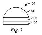
図1は、接着層106によって互いに接着されたLEDダイ102と光学部品104とを含む、代表的なLED光源100の概略断面図を表している。接着層は、非晶質ケイ酸塩網状組織中に表面変性された金属酸化物ナノ粒子類を含む。一般に、LEDダイと光学部品とは、LEDダイによって放射される光が、光学部品へ伝播されてそこへ到達することができるように、光学的に結合されている。光学部品は、光が前記部品の特別な性質に応じて様々な方向に出入り可能な抽出装置であってもよい。
FIG. 1 represents a schematic cross-sectional view of an exemplary
便宜上、LEDダイは、一般的には図1で表されるが、当該技術分野において既知の従来の設計特徴類を包含することもできる。例えば、LEDダイは、窒化物類、例えば、AlN、GaN、InN;リン化物類、例えば、InGaP、AlP、GaP、InP;並びに他のもの、例えば、AlAs、GaAs、InAs、AlSb、GaSb、及びInSbを包含するIII−V族半導体類から典型的に作製される、別個のp型及びn型半導体層を包含することができる。LEDダイはまた、II−VI族半導体、例えば、ZnS、ZnSe、CdSe、及びCdTe;IV族半導体類Ge、Si、及び炭化物類、例えば、SiCから作製することもできる。LEDダイはまた、緩衝層類と、基材層類と、上板層類とを含んでいてもよい。LEDダイの屈折率は、その中に存在する光源の典型的な放射波長では約1.7〜約4.1までの範囲である。 For convenience, the LED die is generally represented in FIG. 1, but can also include conventional design features known in the art. For example, LED dies include nitrides such as AlN, GaN, InN; phosphides such as InGaP, AlP, GaP, InP; and others such as AlAs, GaAs, InAs, AlSb, GaSb, and others. Separate p-type and n-type semiconductor layers can be included, typically made from III-V semiconductors including InSb. LED dies can also be made from II-VI semiconductors such as ZnS, ZnSe, CdSe, and CdTe; IV semiconductors Ge, Si, and carbides such as SiC. The LED die may also include buffer layers, substrate layers, and top plate layers. The refractive index of the LED die ranges from about 1.7 to about 4.1 at the typical emission wavelength of the light source present therein.
矩形のLEDダイが示されているが、切頭型の逆ピラミッドの形を成す、角度のついた側面を有するLEDダイのような、他の既知の形状も考えられる。LEDダイとの電気接点は、便宜上示されていないが、電源を供給してデバイスを作動させるためにいずれか1つ以上の表面上に設けることもできる。例としては、はんだリフロー、ワイヤボンディング、テープ自動化ボンディング(TAB)、又はフリップチップボンディングが挙げられる。構成要素又はチップの個々の層及びその他の機能的要素は、通常、ウェファースケールで形成されており、その後、仕上がったウェファーを個々の部品片にダイスカットして、複数のLEDダイをもたらすことができる。LEDダイは、表面実装、チップオンボード、又は他の既知の実装形態を構成するように構成されてもよい。 Although a rectangular LED die is shown, other known shapes are also conceivable, such as LED dies with angled sides in the form of a truncated inverted pyramid. The electrical contacts with the LED die are not shown for convenience, but can be provided on any one or more surfaces to provide power and operate the device. Examples include solder reflow, wire bonding, tape automated bonding (TAB), or flip chip bonding. Individual layers of components or chips and other functional elements are typically formed on a wafer scale, and the finished wafer can then be diced into individual piece pieces to yield multiple LED dies. it can. The LED die may be configured to constitute surface mount, chip on board, or other known implementation.
本明細書に開示されている光学部品類は、比較的高い屈折率を有する固体の透明な物質から作製されている。光学部品類に好適な材料としては、光学ガラス等の無機材料類、例えば、ショット・ノース・アメリカ社(Schott North America, Inc.)から入手可能なショット(Schott)ガラス型LASF35又はN−LAF34、及び米国特許出願第11/381518号(レザーデイル(Leatherdale)ら)に記載されているものが挙げられ、前記特許出願の開示内容を本明細書に参照として組み込む。他の好適な無機材料類としては、セラミックス、例えば、サファイア、酸化亜鉛、酸化ジルコニウム、ダイアモンド、及び炭化ケイ素が挙げられる。サファイア、酸化亜鉛、ダイアモンド、及び炭化ケイ素は、これらの材料が比較的高い熱伝導率(0.2〜5.0W/cm K)を更に有することから、特に有用である。光学部品は更に、熱硬化性の高屈折率ポリマー類、例えば、アクリル樹脂、エポキシ樹脂、シリコーン樹脂、ポリカーボネート類、及び多環式化合物類、又は熱可塑性の高屈折率ポリマー類、例えば、ポリカーボネート類、及び環状オレフィン類を含んでいてもよい。光学部品は、熱硬化性又は熱可塑性ポリマーを、酸化ジルコニウム、酸化亜鉛、酸化チタン、及び硫化亜鉛を包含するセラミックナノ粒子類と組み合わせて含む場合もある。 The optical components disclosed herein are made from a solid transparent material having a relatively high refractive index. Suitable materials for the optical components include inorganic materials such as optical glass, such as Schott glass type LASF35 or N-LAF34 available from Schott North America, Inc. And in US patent application Ser. No. 11 / 38,518 (Leatherdale et al.), The disclosure of which is incorporated herein by reference. Other suitable inorganic materials include ceramics such as sapphire, zinc oxide, zirconium oxide, diamond, and silicon carbide. Sapphire, zinc oxide, diamond, and silicon carbide are particularly useful because these materials also have a relatively high thermal conductivity (0.2-5.0 W / cm K). The optical component further includes thermosetting high refractive index polymers such as acrylic resins, epoxy resins, silicone resins, polycarbonates, and polycyclic compounds, or thermoplastic high refractive index polymers such as polycarbonates. And cyclic olefins. The optical component may include a thermosetting or thermoplastic polymer in combination with ceramic nanoparticles including zirconium oxide, zinc oxide, titanium oxide, and zinc sulfide.
抽出装置の屈折率は、LEDダイの放射波長では、少なくとも約1.5、例えば、約1.8を超える又は約2を超えてよい。一例では、光学部品の屈折率はLEDダイの光放射面の屈折率と同一であっても、ほぼ同じであっても、又はそれ以下であってもよい。これによって、光を最大限抽出することができる。例えば、屈折率は約0.2以内であってよい。あるいは、抽出装置の屈折率は、LEDダイの光放射面の屈折率よりも大きくあるいは小さくすることができる。例えば、LEDダイの光放射面が1.75である場合、抽出装置の屈折率は1.7、1.75、1.9、2.1、又は2.3であってよい。 The refractive index of the extraction device may be at least about 1.5, such as greater than about 1.8 or greater than about 2, at the emission wavelength of the LED die. In one example, the refractive index of the optical component may be the same as, substantially the same as, or less than the refractive index of the light emitting surface of the LED die. Thereby, light can be extracted to the maximum extent. For example, the refractive index may be within about 0.2. Alternatively, the refractive index of the extraction device can be greater or less than the refractive index of the light emitting surface of the LED die. For example, if the light emitting surface of the LED die is 1.75, the refractive index of the extraction device may be 1.7, 1.75, 1.9, 2.1, or 2.3.
一例では、光学部品は、少なくとも約1.7の屈折率を有する光学ガラスを含む。別の例では、光学部品は、米国特許出願第11/381518号(レザーデイル(Leatherdale)ら)に記載されているような、屈折率が少なくとも約2.0、好ましくは少なくとも2.1、2.2、2.3以上のガラス又はガラス−セラミック材料を含む。一般に、これら材料は、B2O3を20重量%未満、SiO2を20重量%未満、及びP2O5を40重量%未満含む。場合によって、次の材料は20重量%未満に制限される:As2O3、Bi2O3、GeO2、NaO、TeO2、V2O5、SiO2、B2O3、及びP2O5。有用なガラス類又はガラス−セラミック材料類は、Al2O3、TiO2、希土類酸化物類、又はアルカリ土類金属酸化物類等の少なくとも2つの金属酸化物を含む。これら材料類の結晶化温度Txは、好ましくはそれらのガラス転位温度Tgよりも少なくとも5℃高く、そのことが、前記材料の光学部品への封止を助長する。 In one example, the optical component includes an optical glass having a refractive index of at least about 1.7. In another example, the optical component has a refractive index of at least about 2.0, preferably at least 2.1, 2 as described in US patent application Ser. No. 11 / 38,518 (Leatherdale et al.). .2, 2.3 or more glass or glass-ceramic materials. Generally, these materials, B 2 O 3 less than 20 wt%, including SiO 2 less than 20 wt%, and the P 2 O 5 less than 40 wt%. In some cases, the following materials are limited to less than 20% by weight: As 2 O 3 , Bi 2 O 3 , GeO 2 , NaO, TeO 2 , V 2 O 5 , SiO 2 , B 2 O 3 , and P 2. O 5 . Useful glasses or glass - ceramic material such may, Al 2 O 3, TiO 2, including rare earth oxides, or alkaline earth metal oxides of at least two metal oxides and the like. The crystallization temperature T x of these materials is preferably at least 5 ° C. higher than their glass transition temperature T g , which facilitates sealing of the material to optical components.
光学部品の一例は、LEDダイから出る光を抽出するのに使用可能な抽出装置である。一般に、抽出装置は、光の角度分布を調節して、第1光放射パターンを第二の異なる光放射パターンへと変化させる。抽出装置の形によって、放射された光のパターンは、一般に順方向に向いており、抽出装置の周囲を循環していても、幾分対称又は非対称な分布でその側方へ向かっていてもよい。 An example of an optical component is an extraction device that can be used to extract light exiting an LED die. In general, the extraction device adjusts the angular distribution of light to change the first light emission pattern to a second different light emission pattern. Depending on the shape of the extraction device, the emitted light pattern is generally forward-oriented and may circulate around the extraction device or be directed to its side in a somewhat symmetric or asymmetric distribution. .
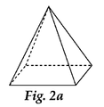
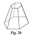
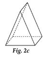
光学部品は、米国特許出願第11/381324号(レザーデイル(Leatherdale)ら)に記載されているような集束性抽出装置(converging extractor)を備えていてよく、この特許出願の開示内容を本明細書に参照として組み込む。集束性抽出装置類(converging extractors)は、少なくとも1つの集束面と、底部と、頂点とを有しており、頂点は、少なくとも一部が底面の上に配置されて、底面よりも小さな表面積を有しており、また、少なくとも一つの集束面は、底面から頂点に向かって集束している。集束性抽出装置(converging extractor)の形は、ピラミッド状、多面体、くさび形、円錐形等、又は幾つかのそれらの組み合わせであることができる。底面は、あらゆる形、例えば、正方形、円形、対称、非対称、規則的、又は不規則にすることができる。頂点は、点、線、又は平坦な若しくは丸みを帯びた表面である場合があり、それは底面の上にあって、底面の中心にあるか又はその中心から離れて歪んでいる。集束性抽出装置(converging extractor)の場合、底面は典型的には、LEDダイと隣接して、一般にはLEDダイと平行に配置されている。更に、底面とLEDダイは、大きさが実質上一致していてもよく、又は底面をLEDダイよりも小さくあるいは大きくすることもできる。 The optical component may comprise a converging extractor as described in US patent application Ser. No. 11 / 38,324 (Leatherdale et al.), The disclosure of which is hereby incorporated by reference. Incorporated in the book as a reference. Converging extractors have at least one focusing surface, a bottom, and a vertex, the vertex being at least partially disposed on the bottom surface and having a smaller surface area than the bottom surface. And at least one focusing surface converges from the bottom surface toward the apex. The shape of the converging extractor can be a pyramid, polyhedron, wedge, cone, etc., or some combination thereof. The bottom surface can be any shape, for example, square, circular, symmetric, asymmetric, regular, or irregular. A vertex may be a point, a line, or a flat or rounded surface, which is above the bottom surface and is distorted at or off the center of the bottom surface. In the case of a converging extractor, the bottom surface is typically located adjacent to the LED die and generally parallel to the LED die. Further, the bottom surface and the LED die may be substantially coincident in size, or the bottom surface may be smaller or larger than the LED die.
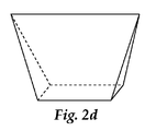
図2a〜2dは、代表的な集束性抽出装置類(converging extractors)の斜視図を示しており、図2aは、四面ピラミッドを示しており、図2bは、六面多角形を示しており、及び図2c及び2dは、頂点(線)が底面よりも上に配置され、頂点がそれぞれ、中心に揃っている及び中心から離れて歪んでいる、くさび形を示している。図2dに示す抽出装置は更に、光を平行にするように作用する2つの発散面をも有しており、集束面によって、その光の向きを前記面の方へ変えることができる。集束性抽出装置類(converging extractors)の別の例は、米国特許出願第11/381324号(レザーデイル(Leatherdale)ら)に示されている。 2a-2d show perspective views of typical converging extractors, FIG. 2a shows a four-sided pyramid, FIG. 2b shows a six-sided polygon, And FIGS. 2c and 2d show a wedge shape in which the vertices (lines) are located above the bottom and the vertices are centered and distorted away from the center, respectively. The extraction device shown in FIG. 2d also has two diverging surfaces that act to collimate the light, and the light can be redirected by the focusing surface toward the surface. Another example of converging extractors is shown in US patent application Ser. No. 11 / 38,324 (Leatherdale et al.).
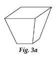
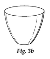
光学部品は、米国特許出願第2006/0091784 A1号(コナー(Connor)ら)、同第2006/0091411 A1号(オーダーカーク(Ouderkirk)ら)、同第2006/0091798 A1号(オーダーカークら)、及び同第2006/0092532 A1号(オーダーカークら)に記載されているような発散性抽出装置(a diverging extractor)を備えていてもよく、これら公報の開示内容を本明細書に参照として組み込む。発散性抽出装置(a diverging extractor)は、少なくとも1つの発散面と、入力面と、入力面よりも広い出力面とを有している。発散性抽出装置類(diverging extractors)は、一般に、先細り形状に成形されている。図3a〜3cは、代表的な発散性抽出装置類(diverging extractors)を表しており、図3aは、4つの面を有する切頭型の逆多角形の斜視図を表しており、図3bは、放物線状の側壁を有する、切頭型の逆先細り形状の斜視図を表しており、図3cは、凸状の出力面を有する、切頭型の逆円錐の概略断面図を表している。 The optical components are US Patent Application Nos. 2006/0091784 A1 (Connor et al.), 2006/0091411 A1 (Ouderkirk et al.), 2006/0091798 A1 (Order Kirk et al.), And a diverging extractor as described in US 2006/0092532 A1 (Order Kirk et al.), The disclosures of which are incorporated herein by reference. A diverging extractor has at least one diverging surface, an input surface, and an output surface wider than the input surface. Diverging extractors are generally shaped into a tapered shape. 3a-3c represent representative diverging extractors, FIG. 3a represents a truncated inverted polygon perspective view with four faces, and FIG. Fig. 3c represents a perspective view of a truncated inverted taper with a parabolic side wall, and Fig. 3c represents a schematic cross-sectional view of a truncated inverted cone having a convex output surface.
発散性抽出装置類(diverging extractors)の例は更に、米国特許出願第11/381518号(レザーデイル(Leatherdale)ら)に以前記載した図4a及び4bにも表されている。これら抽出装置の表面は、LEDダイの中心軸に沿った順方向ではなく、LEDダイからの光を主に横方向に向きを変えるように配置されている。側面放射LED類は、光を短距離に亙って横方向に広がらせて、ディスプレイの表示画面全域に明るい領域と暗い領域又はホットスポット類を回避することができるため、液晶ディスプレイパネル類用の薄型の直接照明型バックライトでの使用に特に適している。 Examples of diverging extractors are also represented in FIGS. 4a and 4b previously described in US patent application Ser. No. 11 / 38,518 (Leatherdale et al.). The surfaces of these extraction devices are arranged to redirect the light from the LED die mainly in the lateral direction rather than in the forward direction along the central axis of the LED die. Side-emitting LEDs can spread light laterally over short distances and avoid bright and dark areas or hot spots across the display screen of the display. It is particularly suitable for use with a thin direct illumination backlight.
図4aは、くさび形抽出装置400の概略断面図である。抽出装置400は、入力面402と、出力面404と、側面406a及び406bとを有している。入力面と出力面は、互いに十分な角度で、通常は約90度で配置されていてよい。この配置により、入力面から入ってくる光線408aは、一方又は両方の側面に(完全に内部反射で、又は反射物質若しくはコーティング(図示せず)の助けを借りて)反射して、光線408bで示されるように、ほぼ横方向に向きを変える。光線408bは、その後、出力面から出る。平面図で提供される抽出装置400の形又は外辺部は、長方形状、台形、パイ型、半円型、又はいずれかのこれらの組み合わせを包含する、様々な形体をとることができる。
FIG. 4 a is a schematic cross-sectional view of the wedge-shaped
図4bは、別のくさび形抽出装置410の概略断面図である。抽出装置410は、入力面412と、出力面414と、側面416とを有している。抽出装置410は、抽出装置400を側面406aと一致する縦軸の周りで回転させた形を有することができる。場合によっては、この抽出装置は、2つの抽出装置400をそれらの各側面406aで結合することによって複合構造で製造することができる。異なる複合構造では、仮想線418によって、抽出装置410を構成する別個の光学体間で起こり得る界面又は境界が表されている。
FIG. 4 b is a schematic cross-sectional view of another wedge-shaped
抽出装置400と同様に、抽出装置410の入力面と出力面は、互いに十分な角度で、名目上約90度で配置されている。LEDから入力面を通って入ってくる光は、一方又は両方の側面に(完全に内部反射で、又は反射物質若しくはコーティング(図示せず)の助けを借りて)反射して、ほぼ横方向に向きを変えた後、出力面から出て行く。平面図(図示せず)によれば、抽出装置410は、例えば、多角形(例えば、正方形又は長方形)、円形、及び楕円形を包含する、あらゆる多数の形を有することができる。円形及び楕円形の形状又は外辺部では、入力面から入ってくる光は、環状の出力光を形成するように向きを変える。
Similar to the
集束性抽出装置類(converging extractors)と同様に、発散性抽出装置(a diverging extractor)の入力面は、典型的に、LEDダイに最も接近して、通常LEDダイと平行して配置される。更に、入力面とLEDダイは、大きさが実質上一致していてもよく、又は入力面をLEDダイよりも小さくあるいは大きくすることもできる発散性抽出装置類(diverging extractors)の他の例は、米国特許第7,009,213 B2号及び米国特許第6,679,621 B2号に記載されている。 Similar to converging extractors, the input surface of a diverging extractor is typically placed closest to the LED die and usually parallel to the LED die. Further, other examples of diverging extractors where the input surface and the LED die may be substantially coincident in size, or the input surface can be smaller or larger than the LED die are: U.S. Pat. No. 7,009,213 B2 and U.S. Pat. No. 6,679,621 B2.
上述のように、LEDダイは、交互に並んだ半導体層を備える。最外層のうち一つは、光放射層と称される場合もあり、また、この層は、光放射面と称される場合がある最も外側の表面を有している。また上述のように、光学部品は光入力面も備える。一つの有用な構造では、LED光源は、例えば図1に示すように光放射面及び光入力面が接着層と接触するように、互いに接着されたLEDダイと光学部品とを備える。 As described above, the LED die includes alternating semiconductor layers. One of the outermost layers is sometimes referred to as a light emitting layer, and this layer has an outermost surface, sometimes referred to as a light emitting surface. As described above, the optical component also includes a light input surface. In one useful structure, the LED light source comprises an LED die and an optical component bonded together such that the light emitting surface and the light input surface are in contact with the adhesive layer, for example as shown in FIG.
光学接着組成物を用いて、接着層を形成する。光学接着組成物は、式(R1SiO1.5)n(OR4)n+2を有するシルセスキオキサンと、式(R2)2Si(OR3)2を有するジアルコキシシラン(前記式中、R1〜R4は有機基であり、nは少なくとも5の整数である。)とを含む。R1は、アルキル基、アルキルアリール基、アリールアルキル基、アリール基、アルコール基、ポリグリコール基、又はポリエーテル基、例えば、メチル基、エチル基、プロピル基、フェニル基、又はナフチル基であり得る。R1及びR2は、同一又は異なっていてよく、それらは、メチル、フェニル、それらの組み合わせ、及びそれらの混合物からなる群より独立して選択されてもよい。例えば、R1及びR2は共にフェニルを含んでもよい。R3及びR4は、同一又は異なっていてよく、それらは、アルキル基、アセトキシ基、メトキシエトキシ基、並びにそれらの組み合わせ、及びそれらの混合物からなる群より独立して選択されてもよい。例えば、R3及びR4は共にメチルを含んでいてよい。更に、nは、少なくとも10又は少なくとも20であってもよい。 An adhesive layer is formed using the optical adhesive composition. The optical adhesive composition comprises silsesquioxane having the formula (R 1 SiO 1.5 ) n (OR 4 ) n + 2 and dialkoxysilane having the formula (R 2 ) 2 Si (OR 3 ) 2 (in the above formula) , R 1 to R 4 are organic groups, and n is an integer of at least 5. R 1 can be an alkyl group, an alkylaryl group, an arylalkyl group, an aryl group, an alcohol group, a polyglycol group, or a polyether group, such as a methyl group, an ethyl group, a propyl group, a phenyl group, or a naphthyl group. . R 1 and R 2 may be the same or different and they may be independently selected from the group consisting of methyl, phenyl, combinations thereof, and mixtures thereof. For example, R 1 and R 2 may both include phenyl. R 3 and R 4 may be the same or different, and they may be independently selected from the group consisting of alkyl groups, acetoxy groups, methoxyethoxy groups, and combinations thereof and mixtures thereof. For example, R 3 and R 4 may both contain methyl. Further, n may be at least 10 or at least 20.
LEDダイと光学部品との間の接着層は、LEDダイと光学部品を互いに接着するときに形成される。光学接着組成物は、反応が進むと非晶質オルガノポリシロキサン網状組織を形成すると考えられる。熱を加えることによって反応が促進する場合がある。非晶質オルガノポリシロキサン網状組織は、オルガノシロキサン前駆体類の縮合に由来する化学結合網状組織を指す。一例では、非晶質オルガノポリシロキサン網状組織は、(R2)2Si(OR3)2を含むD単位に本質的に由来する。 The adhesive layer between the LED die and the optical component is formed when the LED die and the optical component are bonded to each other. The optical adhesive composition is believed to form an amorphous organopolysiloxane network as the reaction proceeds. The reaction may be accelerated by applying heat. Amorphous organopolysiloxane network refers to a chemical bond network derived from condensation of organosiloxane precursors. In one example, the amorphous organopolysiloxane network is essentially derived from D units comprising (R 2 ) 2 Si (OR 3 ) 2 .
シルセスキオキサン類又はポリシルセスキオキサン類は、3個の架橋性酸素原子で配位されたケイ素を有する、基本分子単位に由来する。このため、シルセスキオキサン類は、多種多様な複雑な三次元形状を形成することができる。様々なポリシルセスキオキサン類、例えば、ポリメチルシルセスキオキサン、ポリフェニルシルセスキオキサン、及びポリメチルフェニルシルセスキオキサンを使用することができる。好適な具体的なポリシルセスキオキサン類としては、オハイオ州コロンブス(Columbus)のテクネグラス(Techneglas)から標識GR653L、GR654L、及びGR650Fとして販売されているポリメチルシルセスキオキサン;オハイオ州コロンブスのテクネグラスから標識GR950Fとして販売されているポリフェニルシルセスキオキサン;及びオハイオ州コロンブスのテクネグラスから標識GR908Fとして販売されているポリメチルフェニルシルセスキオキサンが挙げられるが、これらに限定されない。 Silsesquioxanes or polysilsesquioxanes are derived from basic molecular units having silicon coordinated by three crosslinkable oxygen atoms. For this reason, silsesquioxanes can form a wide variety of complex three-dimensional shapes. Various polysilsesquioxanes can be used, such as polymethylsilsesquioxane, polyphenylsilsesquioxane, and polymethylphenylsilsesquioxane. Suitable specific polysilsesquioxanes include polymethylsilsesquioxanes sold under the labels GR653L, GR654L, and GR650F from Techneglas, Columbus, Ohio; Techneglass, Columbus, Ohio Polyphenylsilsesquioxane sold as GR GR from the United States; and polymethyl phenyl silsesquioxane sold as GR GR from the technegrass of Columbus, Ohio.
光学接着組成物は更に、別のアルコキシシラン類、例えば、次の式:
(R1)x−Si−(OR2)y
(前記式中、R1は、アルキル基、アルキルアリール基、アリールアルキル基、アリール基、アルコール基、ポリグリコール基、又はポリエーテル基、又はこれらの組み合わせ若しくは混合物であってよく;R2は、アルキル基、アセトキシ基、又はメトキシエトキシ基、あるいはこれらの混合物であってよく、x+y=4であるとすれば、それぞれ、x=0〜3及びy=4〜1である)を有するテトラアルコキシシラン類及びアルキルトリアルコキシシラン類を含んでいてもよい。モノ−、ジ−、トリ−、及びテトラアルコキシシランを包含する1つ以上のアルコキシシラン類を添加することで、オルガノシロキサン網状組織の架橋密度を制御してもよく、また、可撓性及び接着促進を包含する、オルガノシロキサン網状組織の物理特性を制御してもよい。かかるアルコキシシラン類の例としては、テトラエトキシシラン、テトラメトキシシラン、メチルトリエトキシシラン、及びメチルトリメトキシシランが挙げられるが、これらに限定されない。かかる成分は、約0〜50重量%の量で存在していてよい。
The optical adhesive composition further comprises other alkoxysilanes, such as the following formula:
(R 1) x -Si- (OR 2) y
(Wherein, R 1 represents an alkyl group, an alkylaryl group, an arylalkyl group, an aryl group, an alcohol group, polyglycol group or polyether group or may be a combination of these or mixtures,,; R 2 is A tetraalkoxysilane having an alkyl group, an acetoxy group, or a methoxyethoxy group, or a mixture thereof, where x + y = 4, x = 0-3 and y = 4-1, respectively. And alkyltrialkoxysilanes. The addition density of one or more alkoxysilanes including mono-, di-, tri-, and tetraalkoxysilanes may be added to control the crosslink density of the organosiloxane network, as well as flexibility and adhesion The physical properties of the organosiloxane network, including promotion, may be controlled. Examples of such alkoxysilanes include, but are not limited to, tetraethoxysilane, tetramethoxysilane, methyltriethoxysilane, and methyltrimethoxysilane. Such components may be present in an amount of about 0-50% by weight.
光学接着組成物の粘度を低減し、光学接着組成物のより薄い層をLED放射面又は光学部品のいずれかの上に配置させるために、様々な溶媒類を光学接着組成物に好適に使用するもできる。かかる溶媒類の例としては、アルコール類、ケトン類、エーテル類、アセテート類等が挙げられる。代表的な溶媒類としては、メタノール、エタノール、ブタノール、及び1−メトキシ−2−プロパノールが挙げられる。トルエンやキシレン類等のような芳香族溶媒類が、シルセスキオキサン及びアルコキシシラン中にアリール特性を有する配合物類にとって有用な場合もある。 Various solvents are preferably used in the optical adhesive composition to reduce the viscosity of the optical adhesive composition and to place a thinner layer of optical adhesive composition on either the LED emitting surface or the optical component. You can also. Examples of such solvents include alcohols, ketones, ethers, acetates and the like. Representative solvents include methanol, ethanol, butanol, and 1-methoxy-2-propanol. Aromatic solvents such as toluene and xylenes may be useful for formulations having aryl properties in silsesquioxane and alkoxysilane.
基材への接着性を高めるため、流動特性を調節して基材のコーティングを増強させるため、又は組成物中の構成成分の縮合反応を触媒作用してオルガノポリシロキサン網状組織を形成するために、添加物類を光学接着組成物に添加してもよい。好適な触媒類の例としては、酸類、塩基類、及び金属類の有機錯体類が挙げられる。一つの特別な例では、触媒は、酢酸等の有機酸である。 To increase adhesion to the substrate, to adjust the flow properties to enhance the coating of the substrate, or to catalyze the condensation reaction of the components in the composition to form an organopolysiloxane network Additives may be added to the optical adhesive composition. Examples of suitable catalysts include acids, bases, and organic complexes of metals. In one particular example, the catalyst is an organic acid such as acetic acid.
光学組成物は更に、表面変性された金属酸化物ナノ粒子類を含んでいてもよい。表面変性された金属酸化物ナノ粒子類は、酸化ジルコニウム、酸化チタン、酸化亜鉛、酸化タンタル、酸化ニオブ、酸化ランタン、酸化ストロンチウム、酸化イットリウム、酸化ハフニウム、酸化スズ、酸化アンチモン、及びこれらの組み合わせからなる群より選択される金属酸化物ナノ粒子を含んでいてよい。金属酸化物ナノ粒子類は更に、酸化ケイ素、酸化アルミニウム、酸化ジルコニウム、酸化チタン、酸化亜鉛、酸化タンタル、酸化ニオブ、酸化ランタン、酸化ストロンチウム、酸化イットリウム、酸化ハフニウム、酸化スズ、酸化アンチモン、及びこれらの組み合わせからなる群より選択される少なくとも2つの金属酸化物類の混成金属酸化物ナノ粒子類を含んでいてもよい。酸化チタンナノ粒子類は、ルチル型であっても、アナターゼ型であってもよい。混成金属酸化物ナノ粒子類の特別な例としては、酸化ケイ素と酸化ジルコニウムを含むもの、酸化ケイ素と酸化チタンとを含むもの、酸化ケイ素と酸化ジルコニウムと酸化チタンとを含むものが挙げられる。使用される特別な金属酸化物ナノ粒子類は、屈折率、光学組成物中での相溶性、費用等の様々な因子に左右され得る。 The optical composition may further comprise surface-modified metal oxide nanoparticles. Surface-modified metal oxide nanoparticles include zirconium oxide, titanium oxide, zinc oxide, tantalum oxide, niobium oxide, lanthanum oxide, strontium oxide, yttrium oxide, hafnium oxide, tin oxide, antimony oxide, and combinations thereof. Metal oxide nanoparticles selected from the group may be included. Metal oxide nanoparticles further include silicon oxide, aluminum oxide, zirconium oxide, titanium oxide, zinc oxide, tantalum oxide, niobium oxide, lanthanum oxide, strontium oxide, yttrium oxide, hafnium oxide, tin oxide, antimony oxide, and the like. It may contain hybrid metal oxide nanoparticles of at least two metal oxides selected from the group consisting of: The titanium oxide nanoparticles may be rutile or anatase. Specific examples of hybrid metal oxide nanoparticles include those containing silicon oxide and zirconium oxide, those containing silicon oxide and titanium oxide, and those containing silicon oxide, zirconium oxide and titanium oxide. The particular metal oxide nanoparticles used can depend on various factors such as refractive index, compatibility in the optical composition, cost, and the like.
金属酸化物ナノ粒子類は、金属酸化物ナノ粒子類と接着層及び/又は光学組成物中の他の構成成分類との相溶性を高めるために、1つ以上の表面変性剤類で表面変性されている。例えば、酸化ジルコニウムナノ粒子類は、pH2〜4までの水性酸性環境では安定であり、表面変性を利用して、光学組成物の水性塩基性環境中でのナノ粒子の凝集を防ぐことができる。表面変性は、金属酸化物ナノ粒子類と、ナノ粒子類の表面に付着する表面変性剤(類)やその表面特性を修正する表面変性剤(類)との反応を伴う。 Metal oxide nanoparticles can be surface modified with one or more surface modifiers to enhance the compatibility of the metal oxide nanoparticles with the adhesive layer and / or other components in the optical composition. Has been. For example, zirconium oxide nanoparticles are stable in aqueous acidic environments up to pH 2-4, and surface modification can be used to prevent aggregation of the nanoparticles in the aqueous basic environment of the optical composition. Surface modification involves the reaction of metal oxide nanoparticles with surface modifier (s) that adhere to the surface of the nanoparticles and surface modifier (s) that modify their surface properties.
表面変性剤類は、式A−Bで表すことができ、ここで、A基は、金属酸化物ナノ粒子の表面に付着可能であり、B基は、相溶化基である。一般に、A基は、特定の金属酸化物及び光学組成物の性質を考慮して選択する必要がある。すなわち、表面変性された金属酸化物ナノ粒子類は、非常に塩基性の高い環境でも相溶性が保持されるように、安定でなければならない。有用なA基としては、カルボン酸類、ホスホン酸類、アルコキシシラン類、並びにこれらの組み合わせ及び混合物が挙げられる。アルコキシシラン類は、次の式:
−Si−(OR5)z
(前記式中、R5はアルキル基、アセトキシ基、メトキシエトキシ基、又はこれらの混合物であり、z=1〜3である)で表すことができる。
Surface modifiers can be represented by the formula AB, where the A group can be attached to the surface of the metal oxide nanoparticles and the B group is a compatibilizing group. In general, the A group should be selected in view of the specific metal oxide and the properties of the optical composition. That is, the surface-modified metal oxide nanoparticles must be stable so that compatibility is maintained even in a very basic environment. Useful A groups include carboxylic acids, phosphonic acids, alkoxysilanes, and combinations and mixtures thereof. Alkoxysilanes have the following formula:
-Si- (OR 5) z
(In the above formula, R 5 represents an alkyl group, an acetoxy group, a methoxyethoxy group, or a mixture thereof, and z = 1 to 3).
有用なB基は、金属酸化物ナノ粒子類を光学組成物に相溶化させる親水性基(例としては、アルコール類、ポリグリコール類、及びポリエーテル類が挙げられる)、及び/又は疎水性基(例えばアルキル基)である。表面変性剤類の例としては、ポリエチレングリコールアルコキシシラン類、及びポリエチレングリコール様のカルボン酸誘導体類、例えば、2[−2−(2−メトキシエトキシ)エトキシ]酢酸、及び(2−メトキシエトキシ)酢酸が挙げられる。 Useful B groups are hydrophilic groups that compatibilize the metal oxide nanoparticles in the optical composition (examples include alcohols, polyglycols, and polyethers), and / or hydrophobic groups. (For example, an alkyl group). Examples of surface modifiers include polyethylene glycol alkoxysilanes and polyethylene glycol-like carboxylic acid derivatives such as 2 [-2- (2-methoxyethoxy) ethoxy] acetic acid and (2-methoxyethoxy) acetic acid Is mentioned.
表面変性された金属酸化物ナノ粒子類は、光の波長よりも小さな平均粒度、例えば約300nm未満の平均粒度を有している。 Surface-modified metal oxide nanoparticles have an average particle size that is smaller than the wavelength of light, for example, an average particle size of less than about 300 nm.
用いる場合、表面変性された金属酸化物ナノ粒子類は、重量基準で、オルガノポリシロキサン前駆体の供給源の半分より多い量で存在していてよい。LEDダイと光学部品を互いに接着することで形成される接着層について、表面変性された金属酸化物ナノ粒子類は、接着層の重量に対して約1〜約95重量%までの量で存在していてよい。典型的に、接着層の総重量に対して約40〜約95重量%までの表面変性された金属酸化物ナノ粒子類を有することが望ましい。使用される特定の量は、以下に記載するような接着層に関する所望の屈折率によって一部決定される。しかしながら、接着層内のナノ粒子類の量が多すぎると、LEDダイと光学部品との間で好適な接着が達成し難く、加えて、LED光源の効率が損なわれる場合もある。 When used, the surface-modified metal oxide nanoparticles may be present in an amount greater than half of the organopolysiloxane precursor source on a weight basis. For adhesive layers formed by adhering LED dies and optical components to each other, the surface modified metal oxide nanoparticles are present in an amount from about 1 to about 95 weight percent based on the weight of the adhesive layer. It may be. Typically, it is desirable to have from about 40 to about 95 weight percent surface-modified metal oxide nanoparticles based on the total weight of the adhesive layer. The particular amount used is determined in part by the desired refractive index for the adhesive layer as described below. However, if the amount of nanoparticles in the adhesive layer is too large, it is difficult to achieve suitable adhesion between the LED die and the optical component, and in addition, the efficiency of the LED light source may be impaired.
特に、表面変性された金属酸化物ナノ粒子類は、米国特許第6,376,590 B2号に記載されているナノ粒子のような、屈折率が少なくとも約1.8、好ましくは少なくとも約2.0の非常に結晶性の高いジルコニアナノ粒子を含み、前記特許公報の開示内容を本明細書に参照として組み込む。非常に結晶性の高い酸化ジルコニウムナノ粒子類を、式A−Bに関する上述の1つ以上のアルコキシシラン類で表面変性することによって光学組成物に組み込むことができる。非常に結晶性の高い酸化ジルコニウムナノ粒子類は、式A−Bに関する上述の1つ以上のカルボン酸類で表面変性することによって光学組成物に組み込まれてもよい。非常に結晶性の高い酸化ジルコニウムナノ粒子類の平均粒度は約100nm未満である。 In particular, the surface modified metal oxide nanoparticles have a refractive index of at least about 1.8, preferably at least about 2.1, such as the nanoparticles described in US Pat. No. 6,376,590 B2. 0 containing very highly crystalline zirconia nanoparticles, the disclosure of which is incorporated herein by reference. Highly crystalline zirconium oxide nanoparticles can be incorporated into the optical composition by surface modification with one or more alkoxysilanes as described above for Formulas AB. Very highly crystalline zirconium oxide nanoparticles may be incorporated into the optical composition by surface modification with one or more carboxylic acids as described above for Formula AB. The average particle size of very highly crystalline zirconium oxide nanoparticles is less than about 100 nm.
上述のジルコニアナノ粒子類の屈折率は、非晶質ジルコニアの屈折率よりも極めて大きい。ケイ酸塩網状組織に組み込んで非晶質ケイ酸塩網状組織を提供すると、ジルコニアナノ粒子類は、接着層の屈折率の向上をもたらす。そのため、接着層の光学特性は、接着される特定のLEDダイと光学部品とに依存して、以下に記載するように調節してよい。特に、ケイ酸塩網状組織の屈折率は約1.4であり、表面変性された酸化ジルコニウムナノ粒子類の場合は約1.8〜約2.1である。表面変性された金属酸化物ナノ粒子類は更に、屈折率が約2.0を超える、好ましくは約2.2を超える結晶性酸化チタンナノ粒子類を含んでいてもよい。 The refractive index of the above-mentioned zirconia nanoparticles is much larger than that of amorphous zirconia. When incorporated into a silicate network to provide an amorphous silicate network, the zirconia nanoparticles provide an increase in the refractive index of the adhesive layer. Thus, the optical properties of the adhesive layer may be adjusted as described below, depending on the particular LED die and optical component being bonded. In particular, the refractive index of the silicate network is about 1.4, and in the case of surface-modified zirconium oxide nanoparticles is about 1.8 to about 2.1. The surface modified metal oxide nanoparticles may further comprise crystalline titanium oxide nanoparticles having a refractive index greater than about 2.0, preferably greater than about 2.2.
LED光源の動作効率は、LEDダイと光学部品とが光学結合される程度と直接関与している。本開示内容全体を通して、LEDダイの屈折率への言及は、LEDダイの光放射層の屈折率への言及であることを留意すべきである。LEDダイと光学部品とが光学結合される程度は、接着層の厚さ、並びに接着層、LEDダイ、及び光学部品の屈折率を包含する幾つかの因子に左右される。一般に、接着層の屈折率は、接着層の厚さが、大気中の放射光の波長よりも実質的に小さい、例えば約50nm未満である場合、LEDダイと光学部品との間の光学結合にはあまり重要ではない。厚さが増加するにつれて、接着層の屈折率は、光学結合と関連して更に重要となる。 The operational efficiency of the LED light source is directly related to the degree to which the LED die and the optical component are optically coupled. It should be noted that throughout the present disclosure, reference to the refractive index of the LED die is a reference to the refractive index of the light emitting layer of the LED die. The degree to which the LED die and the optical component are optically coupled depends on several factors including the thickness of the adhesive layer and the refractive index of the adhesive layer, the LED die, and the optical component. In general, the refractive index of the adhesive layer is such that when the thickness of the adhesive layer is substantially less than the wavelength of the emitted light in the atmosphere, for example, less than about 50 nm, the optical coupling between the LED die and the optical component. Is not very important. As the thickness increases, the refractive index of the adhesive layer becomes more important in connection with optical coupling.
接着層は、50nm未満の厚さを有していてよいが、それは通常、約50nmより大きく、例えば、約200nm又は300nmまで、あるいは10μm又は100μmまでである。接着層は、約5nm〜約300nmまで、又は約50nm超〜約100μmまでの厚さを有していてよい。LEDダイと光学部品との間の光学結合を最適化するために、接着層の厚さは、望ましくは、第1表面と第2表面との間の接触面積全体で実質的に均一である。接着層の必要最小限の厚さは、接着される表面の平坦さ又は不規則性に左右される場合がある。 The adhesive layer may have a thickness of less than 50 nm, but it is usually greater than about 50 nm, for example up to about 200 nm or 300 nm, or up to 10 μm or 100 μm. The adhesive layer may have a thickness from about 5 nm to about 300 nm, or from more than about 50 nm to about 100 μm. In order to optimize the optical coupling between the LED die and the optical component, the thickness of the adhesive layer is desirably substantially uniform across the contact area between the first surface and the second surface. The minimum required thickness of the adhesive layer may depend on the flatness or irregularity of the surface to be bonded.
効率を最大にするために、接着層の屈折率は、LEDダイの光放射面(又は前述のような光放射層)の屈折率と、例えば、約0.2以内で正確に一致している。接着層の屈折率が小さすぎると、LEDダイによって放射される光はダイ内に閉じ込められることとなり、接着層自体が非吸収性であっても吸収され失われる。接着層の屈折率を光放射層の屈折率まで高めることにより、LEDによって放射される光の大部分は、接着層が放射光の一部を吸収したとしても、ダイから出て光学部品と結合することができる。 In order to maximize efficiency, the refractive index of the adhesive layer exactly matches the refractive index of the light emitting surface of the LED die (or the light emitting layer as described above), for example, within about 0.2. . If the refractive index of the adhesive layer is too small, the light emitted by the LED die will be confined within the die and will be absorbed and lost even if the adhesive layer itself is non-absorbing. By increasing the refractive index of the adhesive layer to the refractive index of the light emitting layer, the majority of the light emitted by the LED exits from the die and couples with the optical components, even if the adhesive layer absorbs some of the emitted light can do.
上述のように、LEDダイ、又は光放射層のの屈折率は、LEDダイの放射波長では約1.7〜約4.1までの範囲である。表面変性された金属酸化物ナノ粒子類を有しない非晶質オルガノポリシロキサン網状組織の屈折率は、約1.4を超える。表面変性された金属酸化物ナノ粒子類を用いることで、屈折率が約2.4まで向上する。一例では、接着層の屈折率は、LEDダイの放射波長では少なくとも約1.5、例えば、約1.8を超え、又は約2を超える。 As described above, the refractive index of the LED die, or light emitting layer, ranges from about 1.7 to about 4.1 at the emission wavelength of the LED die. The refractive index of the amorphous organopolysiloxane network without surface-modified metal oxide nanoparticles is greater than about 1.4. By using surface-modified metal oxide nanoparticles, the refractive index is improved to about 2.4. In one example, the refractive index of the adhesive layer is at least about 1.5, such as greater than about 1.8, or greater than about 2, at the emission wavelength of the LED die.
特別な例では、LEDダイは、1.9を超える屈折率を有する光放射層を備えており、接着層の厚さは約50nm〜約100μmである。別の例では、LEDダイは、屈折率が1.9以下の光放射層を備えており、接着層の厚さは、約5nm超〜約300nmまでである。 In a particular example, the LED die comprises a light emitting layer having a refractive index greater than 1.9, and the thickness of the adhesive layer is from about 50 nm to about 100 μm. In another example, the LED die includes a light emitting layer having a refractive index of 1.9 or less, and the thickness of the adhesive layer is greater than about 5 nm to about 300 nm.
接着層は、LEDダイによって放射される特定波長の光を実質的に透過する。多くの場合、少なくとも約70%の透過率が望ましく、透過路程長(接着層の厚さ)及び吸収係数を最適化することによって得られる場合もある。 The adhesive layer substantially transmits the specific wavelength of light emitted by the LED die. In many cases, a transmittance of at least about 70% is desirable and may be obtained by optimizing the path length (adhesive layer thickness) and absorption coefficient.
本明細書にはLED光源の製造方法も開示しており、この方法は、a)LEDダイを供給する工程と、b)光学部品を供給する工程と、c)式(R1SiO1.5)n(OR4)n+2を有するシルセスキオキサンと、式(R2)2Si(OR3)2を有するジアルコキシシラン(前記式中、R1〜R4は有機基であり、nは少なくとも5の整数である)と、式(R2)2Si(OR3)2を有するジアルコキシシランとを含む光学接着組成物を供給する工程と、d)LEDダイと光学部品を光学接着組成物に接触させることによって、LEDダイと光学部品を互いに接着する工程と、を含む。 The present specification also discloses a method of manufacturing an LED light source, which includes a) a step of supplying an LED die, b) a step of supplying optical components, and c) a formula (R 1 SiO 1.5 ) N (OR 4 ) Silsesquioxane having n + 2 and dialkoxysilane having the formula (R 2 ) 2 Si (OR 3 ) 2 (wherein R 1 to R 4 are organic groups, n is And an optical adhesive composition comprising a dialkoxysilane having the formula (R 2 ) 2 Si (OR 3 ) 2 , and d) the LED die and the optical component are optically bonded. Adhering the LED die and the optical component to each other by contacting the object.
光学組成物は、LEDダイ又は光学部品のどちらかあるいはこれら両方の1つ以上の表面に、ピペットを用いて、又はディップコーティング、スピンコーティング、エアゾール分配、流し込み、分散、水中溶射によって、又は光学組成物の浴中で表面を結合することによって、あるいは他の同様の方法によって適用してもよい。その後、前記組成物が各表面全体に広がって均質な層を形成するように、それら表面を接触させて光学組成物を挟み込む。気泡が形成される場合、気泡は、減圧することによって取り除くことができる。組立体を次に、それが接着不調を生じることなく処理できるようになるまで、室温で放置させ、これは、数分〜数日であってよい。外部圧縮力又は真空を利用して、接着プロセスを迅速化しても、及び/又は良好な接着を促進してもよい。 The optical composition may be applied to one or more surfaces of either the LED die or the optical component or both using a pipette or by dip coating, spin coating, aerosol dispensing, pouring, dispersion, spraying in water, or optical composition It may be applied by bonding the surfaces in a bath of things or by other similar methods. Thereafter, the optical composition is sandwiched by bringing the surfaces into contact so that the composition spreads over each surface to form a homogeneous layer. If bubbles are formed, they can be removed by reducing the pressure. The assembly is then allowed to stand at room temperature until it can be processed without causing adhesion failure, which may be from minutes to days. External compression forces or vacuum may be utilized to speed up the bonding process and / or promote good bonding.
熱を加えて、接着層の形成及び/又は強化を迅速化してもよいが、組立体の温度は、あらゆる構成要素類の中で最も低いガラス転位温度よりも低く保持しなければならない。約300℃未満、例えば、約200℃未満、又は150℃以下の温度を典型的に使用する。LEDダイと光学部品との熱膨張係数の差によって生じる残留応力及び界面での複屈折を最小限にするために、可能な限り最低の温度を使用することが望ましい。場合によって、接着層の温度は、光源の操作中に達するであろう温度を超えないように注意しなければならない。 Heat may be applied to speed up the formation and / or strengthening of the adhesive layer, but the temperature of the assembly must be kept below the lowest glass transition temperature of all components. Temperatures of less than about 300 ° C, such as less than about 200 ° C, or 150 ° C or less are typically used. It is desirable to use the lowest possible temperature to minimize residual stresses and birefringence at the interface caused by differences in the coefficient of thermal expansion between the LED die and the optical component. In some cases, care must be taken that the temperature of the adhesive layer does not exceed the temperature that would be reached during operation of the light source.
光学接着組成物はまた、LED光源用の封止物質として使用されてもよい。封止物質は、LEDダイと接触させてそれを封入する。 The optical adhesive composition may also be used as a sealing material for LED light sources. The encapsulating material contacts the LED die and encapsulates it.
封止物質は、封止物質が非晶質オルガノポリシロキサン網状組織を含むように、反応した光学接着組成物を含んでいてよく、前記オルガノポリシロキサン網状組織は、(R1SiO1.5)n(前記式中、R1は有機基であり、nは少なくとも10の整数である)に由来するシルセスキオキサン部分を含む。 The encapsulating material may comprise a reacted optical adhesive composition such that the encapsulating material comprises an amorphous organopolysiloxane network, wherein the organopolysiloxane network is (R 1 SiO 1.5 ) a silsesquioxane moiety derived from n (wherein R 1 is an organic group and n is an integer of at least 10).
LED光源は、a)LEDダイを供給する工程と、b)本明細書に記載の光学接着組成物類を供給する工程と、c)LEDダイを前記工程b)で供給された前記組成物のうちいずれかと接触させることによって、組立体を形成する工程と、d)所望により、前記組立体を加熱する工程と、を含む方法によって作製される。 An LED light source comprising: a) a step of supplying an LED die; b) a step of supplying an optical adhesive composition as described herein; and c) an LED die of the composition supplied in step b). It is made by a method comprising the step of forming an assembly by contact with any one of them, and d) optionally heating the assembly.
表面変性された酸化ジルコニウムナノ粒子類は、次のようにして調製した。23重量%ジルコニアゾル(水中固形分25.5重量%であって、固形分は酸化ジルコニウムと酢酸である)100gと、1−メトキシ−2−プロパノール100gと、2−[2−(2−メトキシエトキシ)エトキシ]酢酸(MEEAA)5.45gとを混合して、酸化ジルコニウム1gにつきMEAA1.2ミリモルを有する混合物を得た)。混合物をロータリーエバポレーターに配置して、溶媒を除去した。乾燥した固体が得られ、これを更に60℃において約12時間真空乾燥させた。得られた乾燥粉末をメタノール229.5gに分散させて、ナノ粒子12重量%を有する半透明の液体を形成した。 Surface-modified zirconium oxide nanoparticles were prepared as follows. 23% by weight of zirconia sol (solid content in water is 25.5% by weight, the solid content is zirconium oxide and acetic acid), 100 g of 1-methoxy-2-propanol, 2- [2- (2-methoxy Ethoxy) ethoxy] acetic acid (MEEAA) was mixed with 5.45 g to give a mixture having 1.2 mmol MEAA / g zirconium oxide). The mixture was placed on a rotary evaporator to remove the solvent. A dry solid was obtained, which was further vacuum dried at 60 ° C. for about 12 hours. The obtained dry powder was dispersed in 229.5 g of methanol to form a translucent liquid having 12% by weight of nanoparticles.
ポリ(フェニルシロキサン(C6H5SiO1.5)xガラス樹脂片(テクネグラス(Techneglas)製のGR−950)50gとアセトン115gとを含むシロキサン溶液は、透明な溶液が得られるまでこれら2成分を30分間かき混ぜることによって調製した。 A siloxane solution containing 50 g of poly (phenylsiloxane (C 6 H 5 SiO 1.5 ) x glass resin piece (GR-950 manufactured by Techneglas) and 115 g of acetone is a combination of these two components until a clear solution is obtained. Was prepared by stirring for 30 minutes.
ナノ粒子溶液10gと、シロキサン溶液0.43gと、ジフェニルジメトキシシラン0.3gとを混合することによって、混合物を調製した。ロータリーエバポレーターを用いて溶媒を除去すると、光学接着組成物である粘稠な半透明物質が得られた。
光学ガラス類(LAH−51及びLAH−66、いずれもオハラ社(O’Hara Corp.)製)と、研磨していないサファイア基材(ルビコン・テクノロジー(Rubicon Technology)製)とをアセトン中で11分間、次いでエタノール中で11分間超音波洗浄した。洗浄した表面を乾燥させた。
A mixture was prepared by mixing 10 g nanoparticle solution, 0.43 g siloxane solution, and 0.3 g diphenyldimethoxysilane. When the solvent was removed using a rotary evaporator, a viscous translucent material that was an optical adhesive composition was obtained.
Optical glass (LAH-51 and LAH-66, both manufactured by O'Hara Corp.) and an unpolished sapphire substrate (manufactured by Rubicon Technology) in acetone Sonicate for 11 minutes and then in ethanol for 11 minutes. The cleaned surface was dried.
次いで、光学接着組成物を用いて、各光学ガラスをサファイア基材に接着した。光学ガラスの表面に光学接着組成物を適用して、前記光学接着組成物にサファイア基材を一枚接触させた。適度な圧力を10秒間加えた。結合した試料を、室温で24時間放置した。結合した試料を次に、80℃で4時間加熱し、続いて120℃で4時間加熱した。 Subsequently, each optical glass was adhere | attached on the sapphire base material using the optical adhesive composition. An optical adhesive composition was applied to the surface of the optical glass, and a single sapphire substrate was brought into contact with the optical adhesive composition. A moderate pressure was applied for 10 seconds. The bound sample was left at room temperature for 24 hours. The bonded sample was then heated at 80 ° C. for 4 hours, followed by heating at 120 ° C. for 4 hours.
室温まで冷却させた後、各組立体における接着強さは、ガラスとサファイアとの間に新たに形成された接着を損なわずに処理できるほど十分に高かった。 After cooling to room temperature, the bond strength in each assembly was high enough to be processed without damaging the newly formed bond between glass and sapphire.
光学接着組成物によるLEDの封入
電極付きの京セラ(Kyocera)セラミックパッケージ(京セラ・アメリカ社(Kyocera America, Inc.)、部品番号KD−LA2707−A)に、クリーXT(Cree XT)ダイ(クリー社(Cree Inc.)、部品番号C460XT290−0119−A)を、水性ハロゲン化物フラックス(スーペリア(Superior)30番、スーペリア・フラックス・アンド・マニュファクチュアリング社(Superior Flux & Mfg. Co.))を用いて接着した。LEDパッケージは、0.03mm(1ミル)の金のワイヤを用いてクリーXT(Cree XT)ダイをワイヤボンディングすること(クリック・アンド・ソファ・インダストリーズ社(Kulicke and Soffa Industries, Inc.)4524デジタルシリーズの手動式ワイヤボンディング装置)によって完成した。使用前に、各パッケージは、封入せずにOL 770分光放射計(オプトロニクス・ラボラトリーズ社(Optronics Laboratories, Inc.))を用いて20mAの定電流で試験した。
Encapsulation of LEDs with optical adhesive composition Kyocera ceramic package with electrodes (Kyocera America, Inc., part number KD-LA2707-A), Cree XT (Cree XT) die (Cree) (Cree Inc.), part number C460XT290-0119-A) using an aqueous halide flux (Superior # 30, Superior Flux & Mfg. Co.) Glued. The LED package is wire bonded to a Cree XT die using 0.03 mm (1 mil) gold wire (Kulicke and Soffa Industries, Inc.) 4524 Digital Series manual wire bonding equipment). Prior to use, each package was unsealed and tested at a constant current of 20 mA using an OL 770 spectroradiometer (Optronics Laboratories, Inc.).
京セラ(Kyocera)LEDパッケージ(発光最大約460nm)に、光学接着組成物を約2ミリグラム(mg)入れる。未硬化の封止組成物を有するLEDパッケージを80℃で4時間加熱し、続いて120℃で4時間加熱する。硬化した封止物質は、ピンセットの先を用いた精査に従って、硬化している。LEDの効率は、OL 770分光放射計を用いて測定し、封止前のLEDに比べて増強している。 About 2 milligrams (mg) of optical adhesive composition is placed in a Kyocera LED package (up to about 460 nm emission). The LED package with the uncured sealing composition is heated at 80 ° C. for 4 hours, followed by heating at 120 ° C. for 4 hours. The cured sealing material is cured according to a scrutiny using the tip of the tweezers. The efficiency of the LED is measured using an OL 770 spectroradiometer and is enhanced compared to the LED before sealing.
本発明の趣旨及び範囲から逸脱することなく、本発明の様々な修正及び変更を行えることが当業者には明白であろう。本発明は、本明細書で述べる例示的な実施形態及び実施例によって不当に限定されないこと、また、こうした実施例及び実施形態は、以下に記述する特許請求の範囲のみに限定されるものである、本発明の範疇でのみ例示として示されていることを理解されたい。 It will be apparent to those skilled in the art that various modifications and variations can be made in the present invention without departing from the spirit and scope of the invention. The present invention is not unduly limited by the exemplary embodiments and examples described herein, and such examples and embodiments are limited only to the claims set forth below. It should be understood that these are shown as examples only within the scope of the present invention.
Claims (47)
LEDダイと、
前記LEDダイと光学的に結合した光学部品と、
非晶質オルガノポリシロキサン網状組織を含む接着層と、を含み、前記オルガノポリシロキサン網状組織が式:
(R1SiO1.5)n
(前記式中、R1は有機基であり、nは少なくとも10の整数である。)に由来するシルセスキオキサン部分を含み、
前記接着層が、前記LEDダイと前記光学部品とを互いに接着している、LED光源。 An LED light source, wherein the LED light source is
An LED die,
An optical component optically coupled to the LED die;
An adhesive layer comprising an amorphous organopolysiloxane network, wherein the organopolysiloxane network has the formula:
(R 1 SiO 1.5 ) n
(Wherein R 1 is an organic group and n is an integer of at least 10), including a silsesquioxane moiety derived from
The LED light source, wherein the adhesive layer bonds the LED die and the optical component to each other.
(R2)2Si(OR3)2を含む、請求項1に記載のLED光源。 The amorphous organopolysiloxane network is essentially derived from D-units, the D-units being
The LED light source according to claim 1, comprising (R 2 ) 2 Si (OR 3 ) 2 .
a)LEDダイを供給する工程と、
b)光学部品を供給する工程と、
c)式(R1SiO1.5)n(OR4)n+2を有するシルセスキオキサンと、式(R2)2Si(OR3)2を有するジアルコキシシランとを含む光学接着組成物(前記式中、R1〜R4は有機基であり、nは少なくとも5の整数である。)を供給する工程と、
d)前記LEDダイと前記光学部品とを共に、前記LEDダイ及び前記光学部品を前記光学接着組成物に接触させることによって接着する工程と、を含む、方法。 A method of manufacturing an LED light source, the method comprising:
a) supplying an LED die;
b) supplying an optical component;
c) Optical adhesive composition comprising silsesquioxane having formula (R 1 SiO 1.5 ) n (OR 4 ) n + 2 and dialkoxysilane having formula (R 2 ) 2 Si (OR 3 ) 2 Wherein R 1 to R 4 are organic groups, and n is an integer of at least 5.
d) bonding the LED die and the optical component together by bringing the LED die and the optical component into contact with the optical adhesive composition.
表面変性された金属酸化物ナノ粒子類と、
式(R1SiO1.5)n(OR4)n+2を有するシルセスキオキサンと、
式(R2)2Si(OR3)2を有するジアルコキシシランと、を含み、前記式中、R1〜R4が有機基であり、nが、少なくとも5の整数である、光学接着組成物。 An optical adhesive composition, wherein the optical adhesive composition is
Surface-modified metal oxide nanoparticles,
Silsesquioxane having the formula (R 1 SiO 1.5 ) n (OR 4 ) n + 2 ;
A dialkoxysilane having the formula (R 2 ) 2 Si (OR 3 ) 2 , wherein R 1 to R 4 are organic groups, and n is an integer of at least 5. object.
LEDダイと;
前記LEDダイと接触してそれを封入する封止物質と、を含み、前記封止物質が、請求項32に記載の前記光学接着組成物を含む、LED光源。 An LED light source, wherein the LED light source is
An LED die;
An LED light source comprising: an encapsulant that contacts and encapsulates the LED die, wherein the encapsulant comprises the optical adhesive composition of claim 32.
LEDダイと、
前記LEDダイと接触してそれを封入する封止物質と、を含み、前記封止物質が、非晶質オルガノポリシロキサン網状組織を含み、前記オルガノポリシロキサン網状組織が、式:
(R1SiO1.5)n
(前記式中、R1は有機基であり、nは、少なくとも10の整数である。)に由来するシルセスキオキサン部分を含む、LED光源。 An LED light source, wherein the LED light source is
An LED die,
A sealing material in contact with and encapsulating the LED die, the sealing material comprising an amorphous organopolysiloxane network, wherein the organopolysiloxane network is of the formula:
(R 1 SiO 1.5 ) n
An LED light source comprising a silsesquioxane moiety derived from (wherein R 1 is an organic group and n is an integer of at least 10).
(R2)2Si(OR3)2を含む、請求項43に記載のLED光源。 The amorphous organopolysiloxane network is essentially derived from D-units, the D-units being
(R 2) 2 Si containing (OR 3) 2, LED light source according to claim 43.
a)LEDダイを供給する工程と、
b)本明細書に記載の前記光学接着組成物のうちのいずれかを供給する工程と、
c)前記LEDダイを前記工程b)で供給される前記組成物のうちのいずれかと接触させることにより、組立体を形成する工程と、
d)所望により、前記組立体を加熱する工程と、を含む、方法。 A method of manufacturing an LED light source, the method comprising:
a) supplying an LED die;
b) supplying any of the optical adhesive compositions described herein;
c) contacting the LED die with any of the compositions supplied in step b) to form an assembly;
d) optionally heating the assembly.
Applications Claiming Priority (2)
| Application Number | Priority Date | Filing Date | Title |
|---|---|---|---|
| US86644806P | 2006-11-20 | 2006-11-20 | |
| PCT/US2007/083874 WO2008063884A1 (en) | 2006-11-20 | 2007-11-07 | Optical bonding composition for led light source |
Publications (2)
| Publication Number | Publication Date |
|---|---|
| JP2010510685A true JP2010510685A (en) | 2010-04-02 |
| JP2010510685A5 JP2010510685A5 (en) | 2010-11-18 |
Family
ID=39430044
Family Applications (1)
| Application Number | Title | Priority Date | Filing Date |
|---|---|---|---|
| JP2009538443A Withdrawn JP2010510685A (en) | 2006-11-20 | 2007-11-07 | Optical adhesive composition for LED light source |
Country Status (7)
| Country | Link |
|---|---|
| US (1) | US8013345B2 (en) |
| EP (1) | EP2087532A1 (en) |
| JP (1) | JP2010510685A (en) |
| KR (1) | KR101450929B1 (en) |
| CN (1) | CN101548398A (en) |
| TW (1) | TW200835766A (en) |
| WO (1) | WO2008063884A1 (en) |
Cited By (1)
| Publication number | Priority date | Publication date | Assignee | Title |
|---|---|---|---|---|
| JP2015528829A (en) * | 2012-06-14 | 2015-10-01 | コーニンクレッカ フィリップス エヌ ヴェ | Optical composition |
Families Citing this family (21)
| Publication number | Priority date | Publication date | Assignee | Title |
|---|---|---|---|---|
| EP2727925B1 (en) | 2007-04-17 | 2016-04-06 | Kaneka Corporation | Polyhedral polysiloxane modified product and composition using the modified product |
| JP5814512B2 (en) * | 2009-03-31 | 2015-11-17 | キヤノン株式会社 | OPTICAL MEMBER, ITS MANUFACTURING METHOD, AND OPTICAL SYSTEM |
| KR101749889B1 (en) | 2009-08-12 | 2017-06-22 | 코닌클리케 필립스 엔.브이. | Optical composition |
| US20110062469A1 (en) * | 2009-09-17 | 2011-03-17 | Koninklijke Philips Electronics N.V. | Molded lens incorporating a window element |
| TWI401825B (en) | 2009-11-27 | 2013-07-11 | Ind Tech Res Inst | A bonding method for led chip and bonded led |
| DE102010006072A1 (en) * | 2010-01-28 | 2011-08-18 | OSRAM Opto Semiconductors GmbH, 93055 | Optoelectronic semiconductor device and use of an optoelectronic semiconductor device in a motor vehicle headlamp |
| KR101774306B1 (en) | 2010-05-28 | 2017-09-04 | 가부시키가이샤 가네카 | Polysiloxane composition, hardened material and optical device |
| CN103119048B (en) * | 2010-09-22 | 2016-06-01 | 株式会社钟化 | The polysiloxane-modified body of polyhedral structure, polyhedral structure polysiloxanes system: compositions, solidfied material and luminescent semiconductor device |
| CN202056570U (en) * | 2011-01-20 | 2011-11-30 | 木林森股份有限公司 | Surface-mounted LED (light-emitting diode) with lens |
| US8450445B2 (en) * | 2011-08-17 | 2013-05-28 | Rohm And Haas Electronic Materials Llc | Light emitting diode manufacturing method |
| DE102011111917A1 (en) * | 2011-08-30 | 2013-02-28 | Osram Opto Semiconductors Gmbh | Semiconductor light-emitting device has semiconductor chip that emits monochromatic visible light in wavelength region with respect to light decoupling surface, in which transparent matrix material with silicone and filler are formed |
| US8912024B2 (en) | 2011-11-18 | 2014-12-16 | Invensas Corporation | Front facing piggyback wafer assembly |
| US8900974B2 (en) | 2011-11-18 | 2014-12-02 | Invensas Corporation | High yield substrate assembly |
| DE102012108104A1 (en) * | 2012-08-31 | 2014-03-06 | Osram Opto Semiconductors Gmbh | Optoelectronic device e.g. LED device has beam shaping element that is coupled to semiconductor chip, and through which portion of light emitted from semiconductor chip during operation of electromagnetic radiation is passed |
| TWI480344B (en) | 2012-11-05 | 2015-04-11 | Ind Tech Res Inst | White coating composition, and device employing a coating made of the composition |
| KR101560062B1 (en) * | 2012-11-28 | 2015-10-15 | 주식회사 엘지화학 | Light emitting diode |
| KR102091994B1 (en) | 2012-12-21 | 2020-03-23 | 다우 실리콘즈 코포레이션 | Layered polymer structures and methods |
| US9878954B2 (en) * | 2013-09-13 | 2018-01-30 | 3M Innovative Properties Company | Vacuum glazing pillars for insulated glass units |
| TWI660008B (en) * | 2014-08-26 | 2019-05-21 | 日商琳得科股份有限公司 | Curable composition, method for producing curable composition, cured product, method for using curable composition, and optical device |
| US9946084B2 (en) | 2015-08-10 | 2018-04-17 | Corning Incorporated | Methods for making optical devices |
| TWI735496B (en) * | 2015-12-22 | 2021-08-11 | 日商琳得科股份有限公司 | Curable composition, production method of curable composition, cured product and use method of curable composition |
Family Cites Families (57)
| Publication number | Priority date | Publication date | Assignee | Title |
|---|---|---|---|---|
| DE69715504T2 (en) | 1996-04-26 | 2003-06-05 | Dow Corning Toray Silicone | Electrically conductive silicone rubber composition and its application for the production of semiconductor devices |
| JP3950493B2 (en) | 1996-04-26 | 2007-08-01 | 東レ・ダウコーニング株式会社 | Conductive silicone rubber composition, method for manufacturing semiconductor device, and semiconductor device |
| AU3137097A (en) | 1996-05-16 | 1997-12-05 | Lockheed Martin Energy Systems, Inc. | Low temperature material bonding technique |
| US5777433A (en) | 1996-07-11 | 1998-07-07 | Hewlett-Packard Company | High refractive index package material and a light emitting device encapsulated with such material |
| US5693565A (en) * | 1996-07-15 | 1997-12-02 | Dow Corning Corporation | Semiconductor chips suitable for known good die testing |
| US6548176B1 (en) | 1997-04-03 | 2003-04-15 | The Board Of Trustees Of The Leland Stanford Junior University | Hydroxide-catalyzed bonding |
| US6784463B2 (en) * | 1997-06-03 | 2004-08-31 | Lumileds Lighting U.S., Llc | III-Phospide and III-Arsenide flip chip light-emitting devices |
| US6340824B1 (en) | 1997-09-01 | 2002-01-22 | Kabushiki Kaisha Toshiba | Semiconductor light emitting device including a fluorescent material |
| US6291839B1 (en) | 1998-09-11 | 2001-09-18 | Lulileds Lighting, U.S. Llc | Light emitting device having a finely-patterned reflective contact |
| US6307218B1 (en) | 1998-11-20 | 2001-10-23 | Lumileds Lighting, U.S., Llc | Electrode structures for light emitting devices |
| US6455100B1 (en) | 1999-04-13 | 2002-09-24 | Elisha Technologies Co Llc | Coating compositions for electronic components and other metal surfaces, and methods for making and using the compositions |
| US6376590B2 (en) | 1999-10-28 | 2002-04-23 | 3M Innovative Properties Company | Zirconia sol, process of making and composite material |
| JP2001139894A (en) | 1999-11-15 | 2001-05-22 | Dow Corning Toray Silicone Co Ltd | Adhesive silicone sheet and semiconductor device |
| US7064355B2 (en) * | 2000-09-12 | 2006-06-20 | Lumileds Lighting U.S., Llc | Light emitting diodes with improved light extraction efficiency |
| US7053419B1 (en) | 2000-09-12 | 2006-05-30 | Lumileds Lighting U.S., Llc | Light emitting diodes with improved light extraction efficiency |
| TWI250190B (en) * | 2001-10-03 | 2006-03-01 | Dow Corning Toray Silicone | Adhesive sheet of cross-linked silicone, method of manufacturing thereof, and device |
| US6836602B2 (en) | 2001-10-26 | 2004-12-28 | Corning Incorporated | Direct bonding of optical components |
| US6791120B2 (en) | 2002-03-26 | 2004-09-14 | Sanyo Electric Co., Ltd. | Nitride-based semiconductor device and method of fabricating the same |
| KR20020035819A (en) | 2002-04-25 | 2002-05-15 | 주식회사 포스기술 | Water-proof and dust-free LED matrix module having a reflector plane capable of playing a role of a radiator plate and forming process thereof |
| US6679621B2 (en) | 2002-06-24 | 2004-01-20 | Lumileds Lighting U.S., Llc | Side emitting LED and lens |
| GB0217900D0 (en) | 2002-08-02 | 2002-09-11 | Qinetiq Ltd | Optoelectronic devices |
| TW200406829A (en) | 2002-09-17 | 2004-05-01 | Adv Lcd Tech Dev Ct Co Ltd | Interconnect, interconnect forming method, thin film transistor, and display device |
| US7118438B2 (en) | 2003-01-27 | 2006-10-10 | 3M Innovative Properties Company | Methods of making phosphor based light sources having an interference reflector |
| WO2004077580A2 (en) * | 2003-02-26 | 2004-09-10 | Cree, Inc. | White light source using emitting diode and phosphor and method of fabrication |
| TW200427111A (en) | 2003-03-12 | 2004-12-01 | Shinetsu Chemical Co | Material for coating/protecting light-emitting semiconductor and the light-emitting semiconductor device |
| US7078735B2 (en) | 2003-03-27 | 2006-07-18 | Sanyo Electric Co., Ltd. | Light-emitting device and illuminator |
| US7286296B2 (en) | 2004-04-23 | 2007-10-23 | Light Prescriptions Innovators, Llc | Optical manifold for light-emitting diodes |
| JP4645071B2 (en) * | 2003-06-20 | 2011-03-09 | 日亜化学工業株式会社 | Package molded body and semiconductor device using the same |
| DE102004063978B4 (en) * | 2003-07-17 | 2019-01-24 | Toyoda Gosei Co., Ltd. | Light-emitting device |
| US7009213B2 (en) | 2003-07-31 | 2006-03-07 | Lumileds Lighting U.S., Llc | Light emitting devices with improved light extraction efficiency |
| US6942360B2 (en) | 2003-10-01 | 2005-09-13 | Enertron, Inc. | Methods and apparatus for an LED light engine |
| JP4332407B2 (en) | 2003-10-31 | 2009-09-16 | シャープ株式会社 | Semiconductor light emitting device and manufacturing method thereof |
| KR100592327B1 (en) | 2003-12-19 | 2006-06-21 | 주식회사 코스텍시스 | Light emitting diode module for electronic device |
| JP4231418B2 (en) * | 2004-01-07 | 2009-02-25 | 株式会社小糸製作所 | Light emitting module and vehicle lamp |
| KR100574628B1 (en) | 2004-03-10 | 2006-04-28 | 서울반도체 주식회사 | LED module using Color film |
| US7070300B2 (en) | 2004-06-04 | 2006-07-04 | Philips Lumileds Lighting Company, Llc | Remote wavelength conversion in an illumination device |
| TWI374552B (en) | 2004-07-27 | 2012-10-11 | Cree Inc | Ultra-thin ohmic contacts for p-type nitride light emitting devices and methods of forming |
| JP2006066449A (en) | 2004-08-24 | 2006-03-09 | Toshiba Corp | Semiconductor light emitting device |
| US20060091411A1 (en) | 2004-10-29 | 2006-05-04 | Ouderkirk Andrew J | High brightness LED package |
| US7404756B2 (en) | 2004-10-29 | 2008-07-29 | 3M Innovative Properties Company | Process for manufacturing optical and semiconductor elements |
| US7304425B2 (en) | 2004-10-29 | 2007-12-04 | 3M Innovative Properties Company | High brightness LED package with compound optical element(s) |
| US7330319B2 (en) | 2004-10-29 | 2008-02-12 | 3M Innovative Properties Company | High brightness LED package with multiple optical elements |
| US7329982B2 (en) | 2004-10-29 | 2008-02-12 | 3M Innovative Properties Company | LED package with non-bonded optical element |
| US20060091412A1 (en) | 2004-10-29 | 2006-05-04 | Wheatley John A | Polarized LED |
| US7192795B2 (en) * | 2004-11-18 | 2007-03-20 | 3M Innovative Properties Company | Method of making light emitting device with silicon-containing encapsulant |
| US20060186428A1 (en) * | 2005-02-23 | 2006-08-24 | Tan Kheng L | Light emitting device with enhanced encapsulant adhesion using siloxane material and method for fabricating the device |
| US20060226429A1 (en) | 2005-04-08 | 2006-10-12 | Sigalas Mihail M | Method and apparatus for directional organic light emitting diodes |
| KR20080003876A (en) | 2005-04-14 | 2008-01-08 | 코닌클리즈케 필립스 일렉트로닉스 엔.브이. | Light-emitting device |
| US7494519B2 (en) | 2005-07-28 | 2009-02-24 | 3M Innovative Properties Company | Abrasive agglomerate polishing method |
| US7169031B1 (en) | 2005-07-28 | 2007-01-30 | 3M Innovative Properties Company | Self-contained conditioning abrasive article |
| US7594845B2 (en) | 2005-10-20 | 2009-09-29 | 3M Innovative Properties Company | Abrasive article and method of modifying the surface of a workpiece |
| CN101313417B (en) | 2005-11-22 | 2011-04-20 | 3M创新有限公司 | Arrays of light emitting articles and method of manufacturing same |
| US7285791B2 (en) * | 2006-03-24 | 2007-10-23 | Goldeneye, Inc. | Wavelength conversion chip for use in solid-state lighting and method for making same |
| US7525126B2 (en) | 2006-05-02 | 2009-04-28 | 3M Innovative Properties Company | LED package with converging optical element |
| US20070257270A1 (en) | 2006-05-02 | 2007-11-08 | 3M Innovative Properties Company | Led package with wedge-shaped optical element |
| US7423297B2 (en) | 2006-05-03 | 2008-09-09 | 3M Innovative Properties Company | LED extractor composed of high index glass |
| US7525162B2 (en) * | 2007-09-06 | 2009-04-28 | International Business Machines Corporation | Orientation-optimized PFETS in CMOS devices employing dual stress liners |
-
2007
- 2007-11-07 EP EP07864009A patent/EP2087532A1/en not_active Withdrawn
- 2007-11-07 JP JP2009538443A patent/JP2010510685A/en not_active Withdrawn
- 2007-11-07 KR KR1020097012537A patent/KR101450929B1/en not_active IP Right Cessation
- 2007-11-07 US US12/514,626 patent/US8013345B2/en not_active Expired - Fee Related
- 2007-11-07 CN CNA2007800431142A patent/CN101548398A/en active Pending
- 2007-11-07 WO PCT/US2007/083874 patent/WO2008063884A1/en active Application Filing
- 2007-11-19 TW TW096143724A patent/TW200835766A/en unknown
Cited By (1)
| Publication number | Priority date | Publication date | Assignee | Title |
|---|---|---|---|---|
| JP2015528829A (en) * | 2012-06-14 | 2015-10-01 | コーニンクレッカ フィリップス エヌ ヴェ | Optical composition |
Also Published As
| Publication number | Publication date |
|---|---|
| US8013345B2 (en) | 2011-09-06 |
| TW200835766A (en) | 2008-09-01 |
| EP2087532A1 (en) | 2009-08-12 |
| WO2008063884A1 (en) | 2008-05-29 |
| CN101548398A (en) | 2009-09-30 |
| KR101450929B1 (en) | 2014-10-14 |
| KR20090082496A (en) | 2009-07-30 |
| US20100025711A1 (en) | 2010-02-04 |
Similar Documents
| Publication | Publication Date | Title |
|---|---|---|
| JP2010510685A (en) | Optical adhesive composition for LED light source | |
| JP2010510671A (en) | Optical adhesive composition for LED light source | |
| TWI657599B (en) | Fluorescent substance composition, fluorescent substance sheet, fluorescent substance sheet laminate and led chip using them, led package and method for producing the same | |
| TWI653314B (en) | Light emitting apparatus using composite material, method of manufacturing composite material, and optical film | |
| TWI653495B (en) | Led lighting unit | |
| US9166129B2 (en) | Batwing LED with remote phosphor configuration | |
| US20070241661A1 (en) | High light output lamps having a phosphor embedded glass/ceramic layer | |
| US20060113895A1 (en) | Light emitting device with multiple layers of quantum dots and method for making the device | |
| CN100568552C (en) | Luminaire and manufacture method with layer of photonic crystals of band embedded photoluminescent material | |
| JP2006332682A (en) | Light-emitting device having area of photonic crystal layer and diffusion material, and method for manufacturing same | |
| TWI686963B (en) | Laminate, light-emitting device and manufacturing method thereof, flash lamp and mobile terminal | |
| KR20070110257A (en) | Optically reliable nanoparticle based nanocomposite hri encapsulant and photonic waveguiding material | |
| JP6469004B2 (en) | Optical composition | |
| JP2005109059A (en) | Light-emitting element and manufacturing method thereof | |
| TWI674684B (en) | Light-emitting device and manufacturing method thereof | |
| TWI659834B (en) | Laminate body and method for producing light-emitting device using the same | |
| JP2001024236A (en) | Semiconductor light emitting device | |
| JP2010500747A (en) | Nanoparticle-based inorganic binding materials | |
| TWI476956B (en) | Semiconductor light-emitting device and method of manufacturing the same | |
| JP7323763B2 (en) | Light-emitting device and method for manufacturing light-emitting device | |
| JP2015111626A (en) | Light-emitting device and method of manufacturing the same | |
| CN106935697B (en) | Light emitting device and method for manufacturing the same | |
| KR102561705B1 (en) | Light emitting diode package and manufacturing method thereof | |
| KR102160774B1 (en) | Light emitting device package and method for mafacturing the same |
Legal Events
| Date | Code | Title | Description |
|---|---|---|---|
| A521 | Written amendment |
Free format text: JAPANESE INTERMEDIATE CODE: A523 Effective date: 20100929 |
|
| A621 | Written request for application examination |
Free format text: JAPANESE INTERMEDIATE CODE: A621 Effective date: 20100929 |
|
| A761 | Written withdrawal of application |
Free format text: JAPANESE INTERMEDIATE CODE: A761 Effective date: 20110524 |