JP2010161237A - Method of manufacturing semiconductor device - Google Patents
Method of manufacturing semiconductor device Download PDFInfo
- Publication number
- JP2010161237A JP2010161237A JP2009002930A JP2009002930A JP2010161237A JP 2010161237 A JP2010161237 A JP 2010161237A JP 2009002930 A JP2009002930 A JP 2009002930A JP 2009002930 A JP2009002930 A JP 2009002930A JP 2010161237 A JP2010161237 A JP 2010161237A
- Authority
- JP
- Japan
- Prior art keywords
- heat treatment
- silicon substrate
- silicon region
- silicon
- epitaxial layer
- Prior art date
- Legal status (The legal status is an assumption and is not a legal conclusion. Google has not performed a legal analysis and makes no representation as to the accuracy of the status listed.)
- Pending
Links
Images
Landscapes
- Recrystallisation Techniques (AREA)
Abstract
【課題】結晶欠陥の種類や量を制御することで、所望のスイッチング特性が実現可能となる半導体装置を製造する方法を提供する。
【解決手段】本方法は、シリコン領域形成工程(S30)と、熱処理工程(S32)と、注入工程(S36)を備えている。シリコン領域形成工程では、不純物が含有されているシリコン基板と、シリコン基板の表面に堆積されているエピタキシャル層と、からなるシリコン領域を形成する。熱処理工程では、シリコン領域を熱処理する。素子構造形成工程では、熱処理工程後に、シリコン領域内に半導体装置の素子構造を形成する。注入工程では、熱処理工程後に、シリコン領域内に荷電粒子を注入する。熱処理工程では、熱処理条件を制御することによって、シリコン基板からエピタキシャル層に拡散される不純物の濃度や拡散速度を制御することができる。
【選択図】図2A method of manufacturing a semiconductor device capable of realizing desired switching characteristics by controlling the type and amount of crystal defects is provided.
The method includes a silicon region forming step (S30), a heat treatment step (S32), and an implantation step (S36). In the silicon region forming step, a silicon region including a silicon substrate containing impurities and an epitaxial layer deposited on the surface of the silicon substrate is formed. In the heat treatment step, the silicon region is heat treated. In the element structure forming step, the element structure of the semiconductor device is formed in the silicon region after the heat treatment step. In the implantation step, charged particles are implanted into the silicon region after the heat treatment step. In the heat treatment step, the concentration and diffusion rate of impurities diffused from the silicon substrate to the epitaxial layer can be controlled by controlling the heat treatment conditions.
[Selection] Figure 2
Description
本発明は、半導体装置の製造方法に関する。 The present invention relates to a method for manufacturing a semiconductor device.
シリコン基板内の所定の領域に結晶欠陥を形成することで、シリコン基板内におけるキャリアのライフタイムを制御する技術が知られている。この技術では、シリコン基板内に形成された結晶欠陥が正孔トラップ又は電子トラップとして機能する。正孔トラップ又は電子トラップにキャリアが捕獲されることによって、キャリアの再結合が促進されて半導体装置のスイッチング特性が改善される。 A technique for controlling the lifetime of carriers in a silicon substrate by forming crystal defects in a predetermined region in the silicon substrate is known. In this technique, crystal defects formed in the silicon substrate function as hole traps or electron traps. By trapping carriers in the hole trap or the electron trap, recombination of carriers is promoted, and the switching characteristics of the semiconductor device are improved.
シリコン基板内に結晶欠陥を形成する技術では、一般的に、結晶欠陥を形成する領域(以下、ライフタイム制御領域と称する)に酸素や炭素などの不純物を導入し、その後にライフタイム制御領域に電子線やイオン線などの粒子線を照射する。これによって、シリコン基板内に結晶欠陥が形成され、キャリアのライフタイム制御機能を得ることができる。このような技術の従来例として、例えば特許文献1が挙げられる。 In a technique for forming crystal defects in a silicon substrate, generally, an impurity such as oxygen or carbon is introduced into a region where crystal defects are formed (hereinafter referred to as a lifetime control region), and then the lifetime control region is introduced. Irradiate particle beam such as electron beam and ion beam. Thereby, crystal defects are formed in the silicon substrate, and a carrier lifetime control function can be obtained. As a conventional example of such a technique, for example, Patent Document 1 is cited.
上記した特許文献1の製造方法では、例えばCZ(Czokralski)法又はFZ(Floating Zone)法によって製造されたシリコン基板を利用する。CZ法又はFZ法によって製造されたシリコン基板には、所定の濃度以上の酸素や炭素などの不純物が予め含有されている。このため、CZ法又はFZ法によって製造されたシリコン基板内に結晶欠陥を形成すると、結晶欠陥の種類や量がシリコン基板内に予め含有されている酸素や炭素の濃度によって決定される。CZ法又はFZ法によって製造されたシリコン基板を利用すると、シリコン基板内に形成される結晶欠陥の種類や量を制御することができず、所望のスイッチング特性を得ることができない。 In the manufacturing method of Patent Document 1 described above, a silicon substrate manufactured by, for example, a CZ (Czokralski) method or an FZ (Floating Zone) method is used. A silicon substrate manufactured by the CZ method or the FZ method contains impurities such as oxygen and carbon having a predetermined concentration or more in advance. For this reason, when a crystal defect is formed in a silicon substrate manufactured by the CZ method or the FZ method, the type and amount of the crystal defect are determined by the concentration of oxygen or carbon previously contained in the silicon substrate. When a silicon substrate manufactured by the CZ method or the FZ method is used, the type and amount of crystal defects formed in the silicon substrate cannot be controlled, and desired switching characteristics cannot be obtained.
本発明は上記の課題に鑑みて提案されたものである。本発明は、結晶欠陥の種類や量を制御可能にすることで、所望のスイッチング特性が実現可能となる半導体装置を製造する方法を提供する。 The present invention has been proposed in view of the above problems. The present invention provides a method of manufacturing a semiconductor device in which desired switching characteristics can be realized by making it possible to control the type and amount of crystal defects.
本発明の半導体装置の製造方法は、シリコン領域形成工程と、熱処理工程と、注入工程を備えている。シリコン領域形成工程では、不純物が含有されているシリコン基板と、シリコン基板の表面に堆積されているエピタキシャル層と、からなるシリコン領域を形成する。熱処理工程では、シリコン領域形成工程後に、シリコン領域を熱処理する。注入工程では、熱処理工程後に、シリコン領域内に荷電粒子を注入する。 The method for manufacturing a semiconductor device of the present invention includes a silicon region forming step, a heat treatment step, and an implantation step. In the silicon region forming step, a silicon region including a silicon substrate containing impurities and an epitaxial layer deposited on the surface of the silicon substrate is formed. In the heat treatment step, the silicon region is heat-treated after the silicon region formation step. In the implantation step, charged particles are implanted into the silicon region after the heat treatment step.
本方法では、熱処理工程により、シリコン基板内の不純物がエピタキシャル層に拡散される。このとき、熱処理条件を制御することによって、シリコン基板からエピタキシャル層に拡散される不純物の濃度や拡散速度を制御することができる。注入工程では、シリコン領域のエピタキシャル層内に荷電粒子が注入されて、エピタキシャル層内に結晶欠陥が形成される(ライフタイム制御領域が形成される)。熱処理条件を制御することで、シリコン基板内に予め含有されている不純物の濃度に依存することなく、エピタキシャル層内の不純物濃度が制御でき、エピタキシャル層内の結晶欠陥の種類や量を制御することができる。これによって、所望のキャリアのライフタイム制御機能を得ることができる。 In this method, the impurities in the silicon substrate are diffused into the epitaxial layer by the heat treatment step. At this time, by controlling the heat treatment conditions, the concentration and diffusion rate of impurities diffused from the silicon substrate to the epitaxial layer can be controlled. In the implantation step, charged particles are implanted into the epitaxial layer in the silicon region, and crystal defects are formed in the epitaxial layer (a lifetime control region is formed). By controlling the heat treatment conditions, the impurity concentration in the epitaxial layer can be controlled without depending on the concentration of impurities previously contained in the silicon substrate, and the type and amount of crystal defects in the epitaxial layer can be controlled. Can do. Thereby, a lifetime control function of a desired carrier can be obtained.
本発明の方法によると、結晶欠陥の種類や量を制御することができ、所望のスイッチング特性を備えた半導体装置を製造することができる。 According to the method of the present invention, the type and amount of crystal defects can be controlled, and a semiconductor device having desired switching characteristics can be manufactured.
以下、本発明の実施の形態について詳細に説明する。
(形態1)不純物の拡散範囲に応じて、エピタキシャル層の厚みを制御する。
(形態2)熱処理工程とシリコン領域の表面に熱酸化膜を形成する工程を同一の工程で実施する。
(形態3)ライフタイム制御領域を形成する位置および製造後の半導体装置に要求されるデバイス特性に応じて、熱処理工程における熱処理条件を制御する。
(形態4)素子構造を形成するときに実施する熱処理を考慮して、素子構造形成前の熱処理工程における熱処理条件を決定する。
Hereinafter, embodiments of the present invention will be described in detail.
(Embodiment 1) The thickness of the epitaxial layer is controlled in accordance with the impurity diffusion range.
(Mode 2) The heat treatment step and the step of forming a thermal oxide film on the surface of the silicon region are performed in the same step.
(Mode 3) The heat treatment conditions in the heat treatment step are controlled according to the position where the lifetime control region is formed and the device characteristics required for the semiconductor device after manufacture.
(Embodiment 4) The heat treatment conditions in the heat treatment step before forming the element structure are determined in consideration of the heat treatment performed when the element structure is formed.
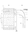
図1(a)に、実施例の製造方法で製造されたダイオード8の断面図を示す。ダイオード8はPINダイオードである。ダイオード8は、シリコン領域6と、アノード電極10と、カソード電極22を備えている。シリコン領域6は、シリコン基板2と、シリコン基板2の表面に堆積されているエピタキシャル層4によって構成されている。シリコン領域6内には、酸素と炭素が含有されている。エピタキシャル層4の表面側には、p−型のアノード層12が形成されている。エピタキシャル層4の裏面側とシリコン基板2の表面側には、n−型のドリフト層18が形成されている。シリコン基板2の裏面側には、n+型のカソード層20が形成されている。エピタキシャル層4内であってアノード層12の下方には、ライフタイム制御領域14が形成されている。ライフタイム制御領域14には、複数の結晶欠陥16が形成されている。アノード電極10は、シリコン領域6の表面に設けられており、アノード層12と接触している。カソード電極22は、シリコン基板6の裏面に設けられており、カソード層20と接触している。ダイオード8では、ライフタイム制御領域14内に形成されている結晶欠陥16が正孔トラップ又は電子トラップとして機能する。正孔トラップ又は電子トラップにキャリアが捕獲されることによって、キャリアの再結合が促進される。
FIG. 1A shows a cross-sectional view of a
図1(b)に、ダイオード8のシリコン領域6内に含有されている酸素と炭素の濃度をダイオード8の深さ方向にプロファイルした結果を示す。参照符号24は、炭素濃度のプロファイル結果を示している。参照符号26は、酸素濃度のプロファイル結果を示している。図1(b)の横軸は不純物濃度を示しており、図の左側に向かうほど不純物濃度が低い。図1(b)の縦軸はダイオード8の深さ方向における位置を示している。図1(b)に示すように、シリコン基板2内では、酸素濃度と炭素濃度は一定である。エピタキシャル層4内では、酸素濃度と炭素濃度はいずれもシリコン基板2から上方に離れるにつれて低下している。炭素濃度はライフタイム制御領域14の下方のエピタキシャル層4内で検出限界以下となっている。このため、ライフタイム制御領域14内には酸素のみ含有されている。ダイオード8では、酸素を欠陥形成要因とする結晶欠陥16がライフタイム制御領域14内に形成され、スイッチング特性が改善されている。
FIG. 1B shows a result of profiling the concentration of oxygen and carbon contained in the
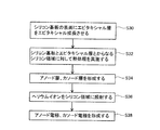
図2に、ダイオード8の製造方法のフローチャートを示す。以下では、ダイオード8を製造する方法を説明する。まず、CZ法又はFZ法によって製造されたシリコン基板2を準備する。シリコン基板2内には、所定の濃度の酸素と炭素が予め含有されている。次に、S30では、準備したシリコン基板2の表面にエピタキシャル層4をエピタキシャル成長させて、シリコン基板2と、シリコン基板2の表面に堆積されているエピタキシャル層4と、からなるシリコン領域6を形成する(シリコン領域形成工程)。シリコン領域形成工程では、エピタキシャル層4をシリコン基板2の表面にエピタキシャル成長させるときにエピタキシャル層4の厚みを制御することで、後述する熱処理工程で酸素と炭素がエピタキシャル層4まで拡散するときの酸素と炭素の拡散範囲を制御することができる。
FIG. 2 shows a flowchart of the manufacturing method of the
次に、S32では、シリコン領域6を熱処理する(熱処理工程)。熱処理工程は拡散炉内で実施することができる。これによって、シリコン基板2内に含有されている酸素と炭素がエピタキシャル層4まで拡散される。このとき、処理時間、処理温度などの熱処理条件を制御することによって、酸素と炭素がエピタキシャル層4まで拡散するときの拡散範囲、拡散速度、拡散濃度などを制御することができる。このため、ライフタイム制御領域14を形成する深さおよび製造後のダイオード8に要求されるデバイス特性に応じて、熱処理工程における熱処理条件を制御することが好ましい。本実施例の製造方法では、ライフタイム制御領域14を形成する深さに、炭素が殆ど含有されず、かつ、酸素が多く含有されるように熱処理条件を制御する。
Next, in S32, the
次に、S34では、シリコン領域6の表面にパターニングされた熱酸化膜を形成し、シリコン領域6の表面からボロンなどのp型の不純物を注入して熱処理する。これによって、エピタキシャル層4の表面側にアノード層12を形成する。なお、上述した熱処理工程とシリコン領域6の表面に熱酸化膜を形成する工程を同一の工程で実施してもよい。同一の工程とすることで、製造工程を短縮することができる。次に、シリコン領域6の裏面からリンなどのn型の不純物を注入して熱処理する。これによって、シリコン基板2の裏面側にカソード層18を形成する。なお、アノード層12とカソード層18を形成するときの熱処理においてもシリコン領域6内の酸素と炭素が拡散される。このため、これらの熱処理を考慮して、熱処理工程における熱処理条件を決定することが好ましい。
Next, in S34, a patterned thermal oxide film is formed on the surface of the
次に、S36では、シリコン領域6の表面からアルミホイル膜を介してヘリウムイオン30を照射する(注入工程)。アルミホイル膜をアブソーバとして利用することで、ヘリウムイオン30をシリコン領域6内の所定の深さ(ライフタイム制御領域14を形成する深さ)に注入することができる。これによって、ライフタイム制御領域14を形成する深さに複数の原子空孔が形成される。形成された原子空孔とライフタイム制御領域14を形成する深さに含有されている酸素とが結合することによって、ライフタイム制御領域14に複数の結晶欠陥16が形成される。注入工程では、ヘリウムイオン30の照射条件を制御することによって、ライフタイム制御領域14内に形成される結晶欠陥16の量を制御することができる。なお、注入工程ではシリコン領域6の裏面からヘリウムイオン30を照射してもよい。
Next, in S36, helium ions 30 are irradiated from the surface of the
S38では、シリコン領域6の表面にアノード層12と接するアノード電極10を形成する。さらに、シリコン領域6の裏面にカソード層20と接するカソード電極22を形成する。これによって、図1(a)に示すダイオード8が完成する。なお、本実施例では、注入工程の後にアノード電極10とカソード電極22を形成しているが、アノード電極10とカソード電極22を形成した後に注入工程を実施してもよい。
In S38, the
本実施例の方法によると、熱処理工程の熱処理条件を制御することで、シリコン基板2内に予め含有されている酸素と炭素の濃度に依存することなく、エピタキシャル層4内に形成される結晶欠陥16の種類や量を制御することができる。CZ法又はFZ法によって製造されたシリコン基板2を利用してダイオード8を製造した場合でも、製造後に良好なキャリアのライフタイム制御機能を得ることができ、所望のスイッチング特性を得ることができる。
また、本実施例の製造方法によると、エピタキシャル層4内に形成される結晶欠陥16の種類を制御することができるため、リーク電流の増加などデバイス特性を悪化させる結晶欠陥16を排除することができる。
さらに、本実施例の製造方法によると、外部からエピタキシャル層4内に酸素又は炭素などの不純物を導入しなくても、エピタキシャル層4内に不純物を含有させることができる。このため、外部からエピタキシャル層4内に不純物を導入するための加速装置などの特別な装置を準備する必要がない。
According to the method of the present embodiment, by controlling the heat treatment conditions of the heat treatment step, crystal defects formed in the epitaxial layer 4 without depending on the concentrations of oxygen and carbon previously contained in the
In addition, according to the manufacturing method of the present embodiment, the types of
Further, according to the manufacturing method of the present embodiment, impurities can be contained in the epitaxial layer 4 without introducing impurities such as oxygen or carbon into the epitaxial layer 4 from the outside. For this reason, it is not necessary to prepare a special device such as an acceleration device for introducing impurities into the epitaxial layer 4 from the outside.
なお、本実施例の製造方法では、シリコン領域形成工程で、シリコン基板2の表面にエピタキシャル層4をエピタキシャル成長させてシリコン領域6を形成したが、シリコン基板2の表面に予めエピタキシャル層4が堆積されているシリコン領域6を準備してもよい。
In the manufacturing method of the present embodiment, the
以上、本発明の実施例について詳細に説明したが、これらは例示に過ぎず、特許請求の範囲を限定するものではない。特許請求の範囲に記載の技術には、以上に例示した具体例を様々に変形、変更したものが含まれる。
本明細書または図面に説明した技術要素は、単独であるいは各種の組合せによって技術的有用性を発揮するものであり、出願時請求項記載の組合せに限定されるものではない。また、本明細書または図面に例示した技術は複数目的を同時に達成し得るものであり、そのうちの一つの目的を達成すること自体で技術的有用性を持つものである。
As mentioned above, although the Example of this invention was described in detail, these are only illustrations and do not limit a claim. The technology described in the claims includes various modifications and changes of the specific examples illustrated above.
The technical elements described in this specification or the drawings exhibit technical usefulness alone or in various combinations, and are not limited to the combinations described in the claims at the time of filing. In addition, the technology exemplified in this specification or the drawings can achieve a plurality of objects at the same time, and has technical usefulness by achieving one of the objects.
2:シリコン基板
4:エピタキシャル層
6:シリコン領域
8:ダイオード
10:アノード電極
12:アノード層
14:ライフタイム制御領域
16:結晶欠陥
18:ドリフト層
20:カソード層
22:カソード電極
S30〜S38:製造方法
2: Silicon substrate 4: Epitaxial layer 6: Silicon region 8: Diode 10: Anode electrode 12: Anode layer 14: Lifetime control region 16: Crystal defect 18: Drift layer 20: Cathode layer 22: Cathode electrodes S30 to S38: Manufacturing Method
Claims (1)
そのシリコン領域形成工程後に、シリコン領域を熱処理する熱処理工程と、
その熱処理工程後に、シリコン領域内に荷電粒子を注入する注入工程を備えていることを特徴とする半導体装置の製造方法。 A silicon region forming step of forming a silicon region comprising a silicon substrate containing impurities and an epitaxial layer deposited on the surface of the silicon substrate;
After the silicon region forming step, a heat treatment step for heat treating the silicon region;
A method of manufacturing a semiconductor device, comprising an injection step of injecting charged particles into a silicon region after the heat treatment step.
Priority Applications (1)
| Application Number | Priority Date | Filing Date | Title |
|---|---|---|---|
| JP2009002930A JP2010161237A (en) | 2009-01-08 | 2009-01-08 | Method of manufacturing semiconductor device |
Applications Claiming Priority (1)
| Application Number | Priority Date | Filing Date | Title |
|---|---|---|---|
| JP2009002930A JP2010161237A (en) | 2009-01-08 | 2009-01-08 | Method of manufacturing semiconductor device |
Publications (1)
| Publication Number | Publication Date |
|---|---|
| JP2010161237A true JP2010161237A (en) | 2010-07-22 |
Family
ID=42578201
Family Applications (1)
| Application Number | Title | Priority Date | Filing Date |
|---|---|---|---|
| JP2009002930A Pending JP2010161237A (en) | 2009-01-08 | 2009-01-08 | Method of manufacturing semiconductor device |
Country Status (1)
| Country | Link |
|---|---|
| JP (1) | JP2010161237A (en) |
Cited By (2)
| Publication number | Priority date | Publication date | Assignee | Title |
|---|---|---|---|---|
| US8698285B2 (en) | 2009-12-16 | 2014-04-15 | Toyota Jidosha Kabushiki Kaisha | Reverse recovery using oxygen-vacancy defects |
| JP2015216371A (en) * | 2014-05-09 | 2015-12-03 | インフィネオン テクノロジーズ アーゲーInfineon Technologies Ag | Method for forming semiconductor device, and semiconductor device |
Citations (5)
| Publication number | Priority date | Publication date | Assignee | Title |
|---|---|---|---|---|
| JPS60198735A (en) * | 1984-03-22 | 1985-10-08 | Matsushita Electronics Corp | Manufacture of semiconductor device |
| JP2006190896A (en) * | 2005-01-07 | 2006-07-20 | Renesas Technology Corp | Epitaxial silicon wafer and its manufacturing method, and semiconductor device and its manufacturing method |
| JP2007251003A (en) * | 2006-03-17 | 2007-09-27 | Toyota Central Res & Dev Lab Inc | Semiconductor device and manufacturing method thereof |
| JP2008147633A (en) * | 2006-12-01 | 2008-06-26 | Applied Materials Inc | Formation and processing of epitaxial layers containing silicon and carbon |
| JP2008177296A (en) * | 2007-01-17 | 2008-07-31 | Toyota Central R&D Labs Inc | Semiconductor device, PN diode, IGBT, and manufacturing method thereof |
-
2009
- 2009-01-08 JP JP2009002930A patent/JP2010161237A/en active Pending
Patent Citations (5)
| Publication number | Priority date | Publication date | Assignee | Title |
|---|---|---|---|---|
| JPS60198735A (en) * | 1984-03-22 | 1985-10-08 | Matsushita Electronics Corp | Manufacture of semiconductor device |
| JP2006190896A (en) * | 2005-01-07 | 2006-07-20 | Renesas Technology Corp | Epitaxial silicon wafer and its manufacturing method, and semiconductor device and its manufacturing method |
| JP2007251003A (en) * | 2006-03-17 | 2007-09-27 | Toyota Central Res & Dev Lab Inc | Semiconductor device and manufacturing method thereof |
| JP2008147633A (en) * | 2006-12-01 | 2008-06-26 | Applied Materials Inc | Formation and processing of epitaxial layers containing silicon and carbon |
| JP2008177296A (en) * | 2007-01-17 | 2008-07-31 | Toyota Central R&D Labs Inc | Semiconductor device, PN diode, IGBT, and manufacturing method thereof |
Cited By (4)
| Publication number | Priority date | Publication date | Assignee | Title |
|---|---|---|---|---|
| US8698285B2 (en) | 2009-12-16 | 2014-04-15 | Toyota Jidosha Kabushiki Kaisha | Reverse recovery using oxygen-vacancy defects |
| US8846544B2 (en) | 2009-12-16 | 2014-09-30 | Toyota Jidosha Kabushiki Kaisha | Reverse recovery using oxygen-vacancy defects |
| JP2015216371A (en) * | 2014-05-09 | 2015-12-03 | インフィネオン テクノロジーズ アーゲーInfineon Technologies Ag | Method for forming semiconductor device, and semiconductor device |
| US9847229B2 (en) | 2014-05-09 | 2017-12-19 | Infineon Technologies Ag | Method for forming a semiconductor device and semiconductor device |
Similar Documents
| Publication | Publication Date | Title |
|---|---|---|
| JP7400874B2 (en) | Semiconductor device and manufacturing method | |
| CN102737967B (en) | Semiconductor device and substrate with chalcogen doped region | |
| EP2930741B1 (en) | Method for manufacturing semiconductor device | |
| CN107408581B (en) | Semiconductor device and method of manufacturing the same | |
| JP6610768B2 (en) | Semiconductor device | |
| JP7351380B2 (en) | semiconductor equipment | |
| JP4919700B2 (en) | Semiconductor device and manufacturing method thereof | |
| KR101916931B1 (en) | Semiconductor epitaxial wafer, method for producing same, and method for manufacturing solid-state imaging element | |
| JP5203667B2 (en) | Manufacturing method of semiconductor device | |
| JP2018137454A (en) | Semiconductor device and manufacturing method of semiconductor device | |
| JP6109432B2 (en) | Method for manufacturing power semiconductor device | |
| JPWO2013046378A1 (en) | IGBT and its manufacturing method | |
| JP5261324B2 (en) | Semiconductor device and manufacturing method thereof | |
| WO2015129430A1 (en) | Semiconductor device and method of manufacturing semiconductor device | |
| JPWO2017002619A1 (en) | Semiconductor device and manufacturing method thereof | |
| JP5528515B2 (en) | SiC bipolar semiconductor device | |
| JP2025179234A (en) | Semiconductor device and method for manufacturing the same | |
| JP2009141304A (en) | Semiconductor device and manufacturing method thereof | |
| JP2010161237A (en) | Method of manufacturing semiconductor device | |
| JP4858527B2 (en) | Manufacturing method of semiconductor device | |
| JP6365790B2 (en) | Semiconductor device and manufacturing method of semiconductor device | |
| JP6976493B1 (en) | Semiconductor devices and their manufacturing methods | |
| JP5080744B2 (en) | Semiconductor device and manufacturing method thereof | |
| JP2017092283A (en) | Semiconductor device and manufacturing method thereof | |
| JP2008172145A (en) | Diode manufacturing method |
Legal Events
| Date | Code | Title | Description |
|---|---|---|---|
| A621 | Written request for application examination |
Free format text: JAPANESE INTERMEDIATE CODE: A621 Effective date: 20110906 |
|
| A131 | Notification of reasons for refusal |
Free format text: JAPANESE INTERMEDIATE CODE: A131 Effective date: 20130827 |
|
| A977 | Report on retrieval |
Free format text: JAPANESE INTERMEDIATE CODE: A971007 Effective date: 20130829 |
|
| A02 | Decision of refusal |
Free format text: JAPANESE INTERMEDIATE CODE: A02 Effective date: 20131217 |