JP2010161202A - Optically coupled device and method of manufacturing the same - Google Patents
Optically coupled device and method of manufacturing the same Download PDFInfo
- Publication number
- JP2010161202A JP2010161202A JP2009002459A JP2009002459A JP2010161202A JP 2010161202 A JP2010161202 A JP 2010161202A JP 2009002459 A JP2009002459 A JP 2009002459A JP 2009002459 A JP2009002459 A JP 2009002459A JP 2010161202 A JP2010161202 A JP 2010161202A
- Authority
- JP
- Japan
- Prior art keywords
- light
- main body
- emitting element
- light emitting
- receiving element
- Prior art date
- Legal status (The legal status is an assumption and is not a legal conclusion. Google has not performed a legal analysis and makes no representation as to the accuracy of the status listed.)
- Pending
Links
- 238000004519 manufacturing process Methods 0.000 title claims description 16
- 230000003287 optical effect Effects 0.000 claims abstract description 140
- 229920005989 resin Polymers 0.000 claims abstract description 110
- 239000011347 resin Substances 0.000 claims abstract description 110
- 239000010954 inorganic particle Substances 0.000 claims abstract description 43
- 238000000034 method Methods 0.000 claims abstract description 10
- GWEVSGVZZGPLCZ-UHFFFAOYSA-N Titan oxide Chemical compound O=[Ti]=O GWEVSGVZZGPLCZ-UHFFFAOYSA-N 0.000 claims abstract description 3
- OGIDPMRJRNCKJF-UHFFFAOYSA-N titanium oxide Inorganic materials [Ti]=O OGIDPMRJRNCKJF-UHFFFAOYSA-N 0.000 claims abstract description 3
- 230000008878 coupling Effects 0.000 claims description 70
- 238000010168 coupling process Methods 0.000 claims description 70
- 238000005859 coupling reaction Methods 0.000 claims description 70
- 239000010445 mica Substances 0.000 claims description 4
- 229910052618 mica group Inorganic materials 0.000 claims description 4
- 239000002245 particle Substances 0.000 claims description 4
- 229910010272 inorganic material Inorganic materials 0.000 claims description 3
- 239000011147 inorganic material Substances 0.000 claims description 3
- 229910052582 BN Inorganic materials 0.000 claims description 2
- PZNSFCLAULLKQX-UHFFFAOYSA-N Boron nitride Chemical compound N#B PZNSFCLAULLKQX-UHFFFAOYSA-N 0.000 claims description 2
- PMHQVHHXPFUNSP-UHFFFAOYSA-M copper(1+);methylsulfanylmethane;bromide Chemical compound Br[Cu].CSC PMHQVHHXPFUNSP-UHFFFAOYSA-M 0.000 claims description 2
- TWNQGVIAIRXVLR-UHFFFAOYSA-N oxo(oxoalumanyloxy)alumane Chemical compound O=[Al]O[Al]=O TWNQGVIAIRXVLR-UHFFFAOYSA-N 0.000 claims description 2
- 230000005540 biological transmission Effects 0.000 abstract description 16
- 238000005538 encapsulation Methods 0.000 abstract 2
- 230000003247 decreasing effect Effects 0.000 abstract 1
- 238000007789 sealing Methods 0.000 description 37
- VYPSYNLAJGMNEJ-UHFFFAOYSA-N Silicium dioxide Chemical compound O=[Si]=O VYPSYNLAJGMNEJ-UHFFFAOYSA-N 0.000 description 6
- 238000007747 plating Methods 0.000 description 5
- 229920001187 thermosetting polymer Polymers 0.000 description 5
- 239000000463 material Substances 0.000 description 4
- 238000010586 diagram Methods 0.000 description 3
- 239000000377 silicon dioxide Substances 0.000 description 3
- 239000007788 liquid Substances 0.000 description 2
- 238000007639 printing Methods 0.000 description 2
- 238000005452 bending Methods 0.000 description 1
- 238000010292 electrical insulation Methods 0.000 description 1
- 239000003822 epoxy resin Substances 0.000 description 1
- 238000010438 heat treatment Methods 0.000 description 1
- 239000011261 inert gas Substances 0.000 description 1
- 230000031700 light absorption Effects 0.000 description 1
- ORQBXQOJMQIAOY-UHFFFAOYSA-N nobelium Chemical compound [No] ORQBXQOJMQIAOY-UHFFFAOYSA-N 0.000 description 1
- 230000010355 oscillation Effects 0.000 description 1
- 230000002093 peripheral effect Effects 0.000 description 1
- 229920000647 polyepoxide Polymers 0.000 description 1
- 229920001721 polyimide Polymers 0.000 description 1
- 239000004065 semiconductor Substances 0.000 description 1
- 229920002050 silicone resin Polymers 0.000 description 1
- 229920001169 thermoplastic Polymers 0.000 description 1
- 239000004416 thermosoftening plastic Substances 0.000 description 1
Images


Classifications
-
- H—ELECTRICITY
- H01—ELECTRIC ELEMENTS
- H01L—SEMICONDUCTOR DEVICES NOT COVERED BY CLASS H10
- H01L25/00—Assemblies consisting of a plurality of individual semiconductor or other solid state devices ; Multistep manufacturing processes thereof
- H01L25/16—Assemblies consisting of a plurality of individual semiconductor or other solid state devices ; Multistep manufacturing processes thereof the devices being of types provided for in two or more different main groups of groups H01L27/00 - H01L33/00, or in a single subclass of H10K, H10N, e.g. forming hybrid circuits
- H01L25/167—Assemblies consisting of a plurality of individual semiconductor or other solid state devices ; Multistep manufacturing processes thereof the devices being of types provided for in two or more different main groups of groups H01L27/00 - H01L33/00, or in a single subclass of H10K, H10N, e.g. forming hybrid circuits comprising optoelectronic devices, e.g. LED, photodiodes
-
- G—PHYSICS
- G02—OPTICS
- G02B—OPTICAL ELEMENTS, SYSTEMS OR APPARATUS
- G02B6/00—Light guides; Structural details of arrangements comprising light guides and other optical elements, e.g. couplings
- G02B6/24—Coupling light guides
- G02B6/42—Coupling light guides with opto-electronic elements
-
- G—PHYSICS
- G02—OPTICS
- G02B—OPTICAL ELEMENTS, SYSTEMS OR APPARATUS
- G02B6/00—Light guides; Structural details of arrangements comprising light guides and other optical elements, e.g. couplings
- G02B6/24—Coupling light guides
- G02B6/42—Coupling light guides with opto-electronic elements
- G02B6/43—Arrangements comprising a plurality of opto-electronic elements and associated optical interconnections
-
- H—ELECTRICITY
- H01—ELECTRIC ELEMENTS
- H01L—SEMICONDUCTOR DEVICES NOT COVERED BY CLASS H10
- H01L2224/00—Indexing scheme for arrangements for connecting or disconnecting semiconductor or solid-state bodies and methods related thereto as covered by H01L24/00
- H01L2224/01—Means for bonding being attached to, or being formed on, the surface to be connected, e.g. chip-to-package, die-attach, "first-level" interconnects; Manufacturing methods related thereto
- H01L2224/42—Wire connectors; Manufacturing methods related thereto
- H01L2224/47—Structure, shape, material or disposition of the wire connectors after the connecting process
- H01L2224/48—Structure, shape, material or disposition of the wire connectors after the connecting process of an individual wire connector
- H01L2224/481—Disposition
- H01L2224/48151—Connecting between a semiconductor or solid-state body and an item not being a semiconductor or solid-state body, e.g. chip-to-substrate, chip-to-passive
- H01L2224/48221—Connecting between a semiconductor or solid-state body and an item not being a semiconductor or solid-state body, e.g. chip-to-substrate, chip-to-passive the body and the item being stacked
- H01L2224/48245—Connecting between a semiconductor or solid-state body and an item not being a semiconductor or solid-state body, e.g. chip-to-substrate, chip-to-passive the body and the item being stacked the item being metallic
- H01L2224/48247—Connecting between a semiconductor or solid-state body and an item not being a semiconductor or solid-state body, e.g. chip-to-substrate, chip-to-passive the body and the item being stacked the item being metallic connecting the wire to a bond pad of the item
-
- H—ELECTRICITY
- H01—ELECTRIC ELEMENTS
- H01L—SEMICONDUCTOR DEVICES NOT COVERED BY CLASS H10
- H01L2924/00—Indexing scheme for arrangements or methods for connecting or disconnecting semiconductor or solid-state bodies as covered by H01L24/00
- H01L2924/30—Technical effects
- H01L2924/301—Electrical effects
- H01L2924/3025—Electromagnetic shielding
-
- H—ELECTRICITY
- H01—ELECTRIC ELEMENTS
- H01L—SEMICONDUCTOR DEVICES NOT COVERED BY CLASS H10
- H01L33/00—Semiconductor devices having potential barriers specially adapted for light emission; Processes or apparatus specially adapted for the manufacture or treatment thereof or of parts thereof; Details thereof
- H01L33/48—Semiconductor devices having potential barriers specially adapted for light emission; Processes or apparatus specially adapted for the manufacture or treatment thereof or of parts thereof; Details thereof characterised by the semiconductor body packages
- H01L33/58—Optical field-shaping elements
Landscapes
- Physics & Mathematics (AREA)
- General Physics & Mathematics (AREA)
- Optics & Photonics (AREA)
- Engineering & Computer Science (AREA)
- Microelectronics & Electronic Packaging (AREA)
- Condensed Matter Physics & Semiconductors (AREA)
- Computer Hardware Design (AREA)
- Power Engineering (AREA)
- Photo Coupler, Interrupter, Optical-To-Optical Conversion Devices (AREA)
- Optical Integrated Circuits (AREA)
Abstract
Description
本発明は、光結合素子及びその製造方法に関する。 The present invention relates to an optical coupling element and a manufacturing method thereof.
光結合素子は、電気信号が入力される発光素子と、電気信号を出力する受光素子と、発光素子から受光素子へと光信号を伝達する光導波路と、を備えている。 The optical coupling element includes a light emitting element that receives an electric signal, a light receiving element that outputs the electric signal, and an optical waveguide that transmits the optical signal from the light emitting element to the light receiving element.
光結合素子としては、例えば、特許文献1乃至3に開示されたものがある。
Examples of the optical coupling element include those disclosed in
特許文献1の光結合素子は、図7に示すように、発光素子101と、受光素子102と、発光素子から受光素子へと光信号を伝達する光導波路としての光透過性の平坦な導波管103と、導波管103に沿って配置された光反射用の複数のホログラフィック素子104と、これらを被覆したパッケージ105と、を備える。特許文献1には、「光がホログラフィック素子104によってのみ反射され、導波管103とパッケージ105との間の界面での光の反射は必要ないため、パッケージ105の材料は反射材料からなる必要がない」旨の記載がある。
As shown in FIG. 7, the optical coupling element of
特許文献2には、該特許文献2の図11に示すように、絶縁性凹ケース内に配置した発光素子と受光素子とを透光性封止層(光導波路に相当)により封止し、更に、その透光性封止層の上に透光性光ガイド板を配置し、透光性光ガイド板及び透光性封止層を遮光体により覆った構成の光結合素子が開示されている。特許文献2の光結合素子の遮光体の下面(透光性光ガイド板の上面に向かう面)には、メッキ又は光反射率の高い樹脂の印刷により形成された反射面が設けられている。
In
特許文献3の光結合素子は、該特許文献3の図1等に示されるように、発光素子と受光素子とが光学的に結合するように対向配置され、対向配置された発光素子及び受光素子を包む中空体の内部に不活性ガスを充填し、且つ、中空体の外周を遮光性樹脂によりモールド成形することにより構成されている。この光結合素子では、中空体の内部空間が光導波路として機能する。
As shown in FIG. 1 and the like of
特許文献1の技術では、高価なホログラフィック素子104を備える必要があるため、材料費が高い、すなわち光結合素子を安価に提供しにくいという課題がある。
In the technique of
特許文献2の技術では、遮光体にメッキ或いは樹脂層を予め形成しておく必要があるため、製造の工程数が多くなるため、やはり、光結合素子を安価に提供しにくいという課題がある。
In the technique of
また、近年、例えば、FA(Factory Automation)機器など、各種機器の小型化が進んでいる。それに伴い、それら機器に搭載される半導体部品(光結合素子を含む)にも、小型化並びに薄型化の要求が高まっている。しかし、特許文献3の技術では、発光素子と受光素子とを対向配置させ、且つ、これら発光素子と受光素子の間に中空を形成する必要があるため、光結合素子の薄型化が困難であるという課題がある。
In recent years, for example, various devices such as FA (Factory Automation) devices have been downsized. Accordingly, there is an increasing demand for miniaturization and thinning of semiconductor components (including optical coupling elements) mounted on these devices. However, in the technique of
このように、薄型の光結合素子を安価に提供することは困難だった。 Thus, it has been difficult to provide a thin optical coupling element at a low cost.
本発明は、相互に電気的に絶縁されている発光素子及び受光素子と、前記発光素子から前記受光素子へと光を伝達する光導波路と、前記光導波路の外面の少なくとも一部を覆う、光反射性無機粒子を含有する樹脂と、を備えることを特徴とする光結合素子を提供する。 The present invention provides a light-emitting element and a light-receiving element that are electrically insulated from each other, an optical waveguide that transmits light from the light-emitting element to the light-receiving element, and light that covers at least a part of the outer surface of the optical waveguide. And a resin containing reflective inorganic particles. An optical coupling element is provided.
この光結合素子によれば、光導波路が光反射性無機粒子を含有する樹脂により覆われているので、発光素子から受光素子へと光導波路を介して好適に光を伝達することができる。 According to this optical coupling element, since the optical waveguide is covered with the resin containing the light-reflecting inorganic particles, light can be suitably transmitted from the light emitting element to the light receiving element via the optical waveguide.
また、光結合素子が高価なホログラフィック素子を備える場合と比べて、光結合素子を安価に提供することができる。また、メッキ或いは樹脂層を予め形成した遮光体により光導波路を覆う構成の光結合素子と比べて、製造工程の工程数を削減することができるため、光結合素子の製造が容易であるとともに、光結合素子を安価に提供することができる。また、発光素子と受光素子とを対向配置させ、且つ、これら発光素子と受光素子の間に中空を形成した構成の光結合素子と比べて、薄型に形成することが可能である。すなわち、本発明によれば、薄型の光結合素子を安価に提供することが可能となる。 Moreover, compared with the case where an optical coupling element is provided with an expensive holographic element, an optical coupling element can be provided at low cost. In addition, since the number of steps of the manufacturing process can be reduced as compared with the optical coupling element configured to cover the optical waveguide with a light shielding body in which plating or a resin layer is formed in advance, the optical coupling element can be easily manufactured, An optical coupling element can be provided at low cost. In addition, the light-emitting element and the light-receiving element can be formed thinner than an optical coupling element having a configuration in which the light-emitting element and the light-receiving element are opposed to each other and a hollow is formed between the light-emitting element and the light-receiving element. That is, according to the present invention, a thin optical coupling element can be provided at a low cost.
また、本発明は、相互に電気的に絶縁されている発光素子及び受光素子の前記発光素子から前記受光素子へと光導波路を介して光を伝達可能となるように、該光導波路を設ける第1工程と、前記光導波路を、光反射性無機粒子を含有する樹脂により覆う第2工程と、をこの順に行うことを特徴とする光結合素子の製造方法を提供する。 Further, the present invention provides a light-emitting element and a light-receiving element that are electrically insulated from each other, wherein the light guide is provided so that light can be transmitted from the light-emitting element to the light-receiving element via the optical waveguide. There is provided a method for manufacturing an optical coupling element, characterized in that one step and a second step of covering the optical waveguide with a resin containing light-reflective inorganic particles are performed in this order.
本発明によれば、薄型の光結合素子を安価に提供することが可能となる。 According to the present invention, a thin optical coupling element can be provided at low cost.
以下、本発明の実施形態について、図面を用いて説明する。なお、すべての図面において、同様の構成要素には同一の符号を付し、適宜に説明を省略する。 Hereinafter, embodiments of the present invention will be described with reference to the drawings. In all the drawings, the same components are denoted by the same reference numerals, and description thereof will be omitted as appropriate.
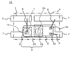
図1は実施形態に係る光結合素子10を示す断面図、図2は光結合素子10の平面図である。なお、図2では、封止樹脂4を仮想線(2点鎖線)で示し、該封止樹脂4の内部の構成を見せている。
FIG. 1 is a sectional view showing an
本実施形態に係る光結合素子10は、相互に電気的に絶縁されている発光素子1及び受光素子2と、発光素子1から受光素子2へと光を伝達する光導波路3と、光導波路3の外面の少なくとも一部を覆う、光反射性無機粒子を含有する樹脂(封止樹脂4)と、を備える。また、本実施形態に係る光結合素子の製造方法では、互に電気的に絶縁されている発光素子1及び受光素子2の発光素子1から受光素子2へと光を伝達する光導波路3を設ける第1工程と、光導波路3を光反射性無機粒子を含有する樹脂(封止樹脂4)により覆う第2工程と、をこの順に行う。以下、詳細に説明する。
The
先ず、光結合素子10の構成を説明する。
First, the configuration of the
図1及び図2に示すように、本実施形態に係る光結合素子10は、相互に電気的に絶縁されている発光素子1及び受光素子2と、発光素子1から受光素子2へと光を伝達する光導波路3と、光導波路3を覆う封止樹脂4と、を備えている。
As shown in FIGS. 1 and 2, the
封止樹脂4は、詳細を後述するように、光反射性無機粒子を含有する絶縁性樹脂からなり、光導波路3内を伝達される光を該光導波路3内に閉じ込める機能を奏する。
As will be described in detail later, the sealing
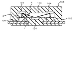
図6は発光素子1の構造の一例を示す斜視図である。図6に示すように、発光素子1は、例えば、その上面に電極1a(電極パッド)を、下面(裏面)に裏面電極(図示略)を、それぞれ備えている。更に、発光素子1は、発光部としてのPNジャンクション1bを備えている。このような発光素子1は、該発光素子1の外面から外部へ発光する。
FIG. 6 is a perspective view showing an example of the structure of the
また、受光素子2は、例えば、その上面に、電極2aと、受光部2bと、を備える。この受光素子2は、発光素子1から発光され光導波路3を介して伝達される光を受光部2bにおいて受光する。
The light receiving
図1及び図2に示すように、発光素子1と受光素子2とは、例えば、同一平面上に配置されている。具体的には、例えば、発光素子1は、その裏面電極がパッケージ(Package)端子(基台)7と導通するように、該パッケージ端子7上に配置されている。また、受光素子2は、発光素子1が配置されているのとは別のパッケージ端子7上に配置されている。発光素子1の電極1aと、受光素子2の電極2aは、それぞれボンディングワイヤ6を介して別のパッケージ端子7に対して電気的に接続されている。発光素子1の電極1aが接続されたパッケージ端子7並びに裏面電極が接続されたパッケージ端子7と、受光素子2の電極2aが接続されたパッケージ端子7とは、相互に電気的に絶縁されている。すなわち、発光素子1と受光素子2とは相互に電気的に絶縁されている。なお、各パッケージ端子7は、例えば、後述するように、1つのリードフレーム5の一部分ずつからなることが挙げられる。
As shown in FIG.1 and FIG.2, the
光導波路3は、例えば、平板な板状に形成された本体部30と、本体部30と発光素子1とを相互に接続した第1接続部31と、本体部30と受光素子2の受光部2bとを相互に接続した第2接続部32と、からなる。本体部30は、第1及び第2接続部31、32をそれぞれ介して発光素子1から受光素子2に亘って架設されている。この光導波路3においては、第1接続部31は発光素子1から本体部30へ、本体部30は第1接続部31から第2接続部32へ、第2接続部32は本体部30から受光素子2へ、順次に光を伝達する。
The
本体部30は、例えば、予め成型された、光透過性且つ絶縁性のフィルムからなる。このようなフィルムは、例えば、ポリイミドフィルムであることが挙げられる。本体部30は、第1接続部31から第2接続部32に亘って架設されている。この本体部30の下面は、受光素子2の受光部2bに面している。
The
第1接続部31は、例えば、光透過性且つ絶縁性で、粘性が高い液状の樹脂(以下、単に光透過性樹脂)を発光素子1へ滴下した後で硬化させることにより構成されている。同様に、第2接続部32は、第1接続部31を構成しているのと同様の光透過性樹脂を受光素子2において少なくとも受光部2bを含む部分へ滴下した後で硬化させることにより構成されている。このような光透過性樹脂としては、例えば、熱硬化性のシリコーン樹脂が挙げられる。
The
第1及び第2接続部31、32の高さ(上下寸法)の調節は、その光透過性樹脂の滴下量及び滴下範囲を調節することにより行うことができる。図1に示すように、例えば、発光素子1よりも受光素子2の方が高い(上下寸法が大きい)。このため、発光素子1における本体部30側の面(つまり発光素子1の上面)と、受光素子2における本体部30側の面(つまり受光素子2の上面)とは、本体部30の下面からの距離が互いに異なる。この場合にも、第1接続部31における本体部30側の面と、第2接続部32における本体部30側の面と、が相互に面一となるように、第1接続部31の方が第2接続部32よりも高く形成されている。すなわち、第1接続部31における本体部30側の面と、第2接続部32における本体部30側の面と、が相互に面一となるように、第1及び第2接続部31、32の高さがそれぞれ設定されている。これにより、本体部30の下面は受光素子2の受光部2bに対し略平行に配置されている。この構造により、本体部30から第2接続部32を介して受光部2bへ伝達される光の伝達効率が高められている(光の損失が低減されている)。
The height (vertical dimension) of the first and
なお、詳細には、第1及び第2接続部31、32を構成する光透過性の樹脂をそれぞれ滴下後に、これら滴下した双方の樹脂に亘って本体部30を架設した後で、これら双方の樹脂が硬化されている。これにより、第1接続部31は発光素子1と本体部30とを相互に接続(接着)している一方で、第2接続部32は受光素子2と本体部30とを相互に接続(接着)している。
In more detail, after each of the light-transmitting resins constituting the first and
また、第1接続部31は、発光素子1の全体(リードフレーム5に設けられた面を除く)を被覆するように形成されている。これにより、発光素子1の(リードフレーム5に設けられた面を除く)いずれの面から出力される光も、第1接続部31を介して本体部30へ伝達され得るようになっている。
The
また、第1接続部31と第2接続部32とは相互に離間し、第1接続部31と第2接続部32との間には封止樹脂4が介在している。これにより、発光素子1からの発光は、受光素子2へと直線的に伝達されるのではなく、第1接続部31、本体部30及び第2接続部32をこの順に介して、受光部2bに向けて伝達される。よって、第1接続部31と第2接続部32との間での光の損失を低減することができる。
Further, the
封止樹脂4は、光反射性無機粒子を含有する絶縁性樹脂である。
The sealing
この光反射性無機粒子としては、該光反射性無機粒子により発光素子1の発振波長の光を反射し、該波長の光をほとんど透過させない無機材質の粒子が好適に用いられる。
As the light-reflective inorganic particles, particles made of an inorganic material that reflects the light having the oscillation wavelength of the light-emitting
光反射性無機粒子の反射性能をより高めるため、光反射性無機粒子は、その平面形状のアスペクト比(短辺と長辺の寸法比)が、例えば、2以上であることが好ましく、3以上であることがより好ましい。これは、光反射性無機粒子が球形に近いと、該光反射性無機粒子の表面で光の散乱が繰り返される結果、光が封止樹脂4の内部深くまで達して吸収される可能性が生じるためである。これに対し、光反射性無機粒子の平面形状のアスペクト比を例えば2以上とすることにより、光導波路3との境界部付近の封止樹脂4内の光反射性無機粒子によって光を好適に光導波路3側へ反射させることができるので、光が封止樹脂4の内部深くまで達して吸収されてしまう可能性を低減できる。光反射性無機粒子の具体的な形状は、球形又はフレーク状などの扁平形状であることが挙げられるが、光反射性無機粒子の反射性能向上の観点からは、光反射性無機粒子が扁平形状である方が好ましい。
In order to further improve the reflection performance of the light-reflecting inorganic particles, the light-reflecting inorganic particles preferably have a planar aspect ratio (dimensional ratio of short side to long side) of, for example, 2 or more. It is more preferable that This is because, when the light-reflective inorganic particles are nearly spherical, light is repeatedly scattered on the surface of the light-reflective inorganic particles, so that the light may reach deep inside the sealing
このような光反射機能を実現する光反射性無機粒子の具体例としては、例えば、酸化チタン、酸化アルミ、マイカ(雲母)、窒化アルミ、ボロンナイトライドのうちの少なくとも何れか1種の無機材料の粒子が挙げられる。 Specific examples of the light-reflecting inorganic particles that realize such a light-reflecting function include, for example, at least one inorganic material selected from titanium oxide, aluminum oxide, mica (mica), aluminum nitride, and boron nitride. Particles.
この絶縁性樹脂中の光反射性無機粒子の含有率は、例えば、15重量%以上25重量%以下であることが好ましい。具体的には、例えば、20重量%程度とすることができる。また、光反射性無機粒子の粒径(長辺の長さ)は、例えば、25nm以上35nm以下とすることができ、具体的には、例えば、30nm程度とすることができる。 The content ratio of the light-reflective inorganic particles in the insulating resin is preferably 15% by weight or more and 25% by weight or less, for example. Specifically, for example, it can be about 20% by weight. The particle size (long side length) of the light-reflective inorganic particles can be, for example, 25 nm or more and 35 nm or less, and specifically, for example, about 30 nm.
また、このような光反射性無機粒子を含有する絶縁性樹脂としては、例えば、熱硬化性のエポキシ樹脂が挙げられる。 Examples of the insulating resin containing such light-reflective inorganic particles include a thermosetting epoxy resin.
なお、封止樹脂4は、他に、例えば、50〜60重量%のシリカも含有している。シリカは、一般的な封止樹脂材料に含有されているが、このシリカのみを含有する樹脂では好適に光を反射することができない。このため、本実施形態では、封止樹脂4に上述のような光反射性無機粒子を含有させている。
In addition, the sealing
この封止樹脂4は、光導波路3の外面のうち、発光素子1、受光素子2及びパッケージ端子7の何れにも接していない部分の全体を覆っている。具体的には、例えば、図1及び図2に示すように、各パッケージ端子7の一部のみが封止樹脂4の外部に露出し、光結合素子10におけるその他の各部(発光素子1、受光素子2、光導波路3、ボンディングワイヤ6、及び、各パッケージ端子7の一部)は封止樹脂4内に位置している。
The sealing
次に、本実施形態に係る光結合素子の製造方法を説明する。 Next, a method for manufacturing the optical coupling element according to this embodiment will be described.
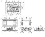
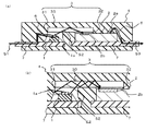
図3は実施形態に係る光結合素子の製造方法の一連の工程を示す断面図である。また、図4は図3の後の製造工程を説明するための図であり、図4(a)、図4(b)、図4(d)はそれぞれ平面図、図4(c)、図4(e)、図4(f)はそれぞれ断面図である。 FIG. 3 is a cross-sectional view showing a series of steps in the method of manufacturing the optical coupling element according to the embodiment. 4 is a diagram for explaining the manufacturing process subsequent to FIG. 3. FIGS. 4 (a), 4 (b), and 4 (d) are plan views, FIG. 4 (c), and FIG. 4 (e) and 4 (f) are cross-sectional views, respectively.
先ず、図3(a)に示すように、1つのリードフレーム5上に発光素子1及び受光素子2をマウントボンディングする。すなわち、リードフレーム5上に発光素子1及び受光素子2をそれぞれ設置し、発光素子1の電極1a、受光素子2の電極2aをそれぞれボンディングワイヤ6を介してリードフレーム5に対し電気的に接続する。なお、発光素子1と受光素子2とは、同一平面上に配置される。また、発光素子1が設置される部分と、電極1aが接続される部分と、受光素子2が設置される部分と、電極2aが接続される部分は、後で切断されて、互いに別体のパッケージ端子7となる。
First, as shown in FIG. 3A, the
次に、図3(b)に示すように、発光素子1と受光素子2へそれぞれ液状の光透過性樹脂41、42を滴下する。これら光透過性樹脂41、42は、後で硬化されることにより、それぞれ第1接続部31、第2接続部32(それぞれ図3(c)参照)を構成する。ここで、本実施形態の場合、例えば、発光素子1よりも受光素子2の方が高い(上下寸法が大きい)が、第1接続部31における本体部30側の面と、第2接続部32における本体部30側の面と、が相互に面一となるように、光透過性樹脂41、42の各々の滴下量及び滴下範囲を設定する。具体的には、光透過性樹脂42は、例えば、図3(b)に示すように、受光部2b上に扁平に広がるように、その滴下量及び滴下範囲を設定する。対して、光透過性樹脂41は、例えば、図3(b)に示すように、発光素子1の上面よりも上方に盛り上がり、該光透過性樹脂41の上端が光透過性樹脂42の上端と同程度の高さに達するように、その滴下量及び滴下範囲を設定する。しかも、第1接続部31と第2接続部32とが相互に離間し、第1接続部31と第2接続部32との間に(後で形成される)封止樹脂4が介在するように、光透過性樹脂41、42の各々の滴下量及び滴下範囲を設定する。
Next, as shown in FIG. 3B, liquid light-transmitting
次に、本体部30を光透過性樹脂41から光透過性樹脂42に亘って架設する(図3(c)参照)。次に、図3(c)に示すように、光透過性樹脂41、42を例えば熱硬化により硬化させる。これにより、光透過性樹脂41は第1接続部31となって発光素子1と本体部30とを相互に接続(接着)する。同様に、光透過性樹脂42は第2接続部32となって本体部30と受光素子2とを相互に接続(接着)する。こうして、本体部30が、第1及び第2接続部31、32をそれぞれ介して発光素子1から受光素子2に亘って架設された状態となるとともに、本体部30、第1接続部31及び第2接続部32は相互に一体化されて光導波路3を構成する。このようにして、相互に電気的に絶縁されている発光素子1及び受光素子2の発光素子1から受光素子2へと光を伝達する光導波路3が設けられる。
Next, the
次に、光結合素子10における所要部位(発光素子1、受光素子2、光導波路3、ボンディングワイヤ6、及び、各パッケージ端子7の一部)を覆う型枠(金型:図示略)を配置した状態で、該型枠内に、封止樹脂4を構成する樹脂、すなわち、光反射性無機粒子を含有する樹脂を注入する。次に、注入した樹脂を、例えば熱硬化により硬化させる。これにより、図3(d)に示すように、封止樹脂4が成型される。
Next, a mold (mold: not shown) is arranged to cover a required portion (light emitting
図4(a)は、図3(d)の状態でのリードフレーム5の全体形状を示す平面図である。なお、図4(a)では、封止樹脂4を仮想線(2点鎖線)で示し、封止樹脂4の内部を見せている。
FIG. 4A is a plan view showing the overall shape of the
次に、図4(b)及び図4(c)に示すように、リードフレーム5を切断位置a、bで切断し、リードフレーム5の周縁部を除去する。リードフレーム5において、切断位置a、bで切断することにより除去した残りの部分、すなわち、それぞれの一部が封止樹脂4内に入り込んでいる部分は、パッケージ端子7となる。
Next, as shown in FIGS. 4B and 4C, the
次に、図4(d)及び図4(e)に示すように、各パッケージ端子7を折り曲げ位置c、d、e、fでそれぞれ折り曲げ加工することにより、図4(f)に示すように、各パッケージ端子7を屈曲させる。
Next, as shown in FIG. 4D and FIG. 4E, each
以上により、光結合素子10が製造される。
Thus, the
次に、光結合素子10の動作を説明する。
Next, the operation of the
図5は光結合素子10による信号(電気信号及び光信号)の伝達態様を模式的に示す図であり、図5(a)は光結合素子10の全体での信号の流れを示し、図5(b)は光導波路3での光信号の流れを示す。
FIG. 5 is a diagram schematically illustrating how signals (electrical signals and optical signals) are transmitted by the
発光素子1は、発光側の(発光素子1の電極1aに接続されている)パッケージ端子7を及びボンディングワイヤ6を介して該発光素子1に入力される電気信号S1(図5(a))に従って発光動作を行う。すなわち、発光素子1は、パッケージ端子7を介して入力される電気信号を光信号に変換し、該光信号S2(図5(a)、図5(b))を光導波路3の第1接続部31へ出力する。
The
発光素子1が出力する光信号S2は、第1接続部31、本体部30、及び第2接続部32をこの順に介して、受光素子2の受光部2bへ伝達される。すなわち、第1接続部31、本体部30、及び第2接続部32からなる光導波路3は、発光素子1と受光素子2の受光部2bとを光結合している。
The optical signal S2 output from the
上述のように、発光素子1が接続されたパッケージ端子7と、受光素子2が接続されたパッケージ端子7とは、相互に電気的に絶縁されているため、発光素子1と受光素子2とは相互に電気的に絶縁されており、光信号S2のみが光導波路3を介して発光素子1から受光素子2へと伝達される。また、封止樹脂4、本体部30を構成するフィルム、及び、第1及び第2接続部31、32を構成する光透過性樹脂は、それぞれ絶縁性のものであるため、発光素子1のパッケージ端子7と受光素子2側のパッケージ端子7との間に大きな電位差が発生しても、発光素子1と受光素子2との間の電気的絶縁を確保することができる。
As described above, since the
また、光導波路3は、光反射性無機粒子を含有する樹脂からなる封止樹脂4により覆われているため、高い光伝達効率で、光信号S2を伝達することができる。
Moreover, since the
受光素子2は、受光部2bにて受光した光信号S2を電気信号S3(図5(a))に変換し、該電気信号S3を電極2aから出力する。この電気信号S3は、ボンディングワイヤ6及びパッケージ端子7を介して光結合素子10の外部へ出力される。
The
以上のような実施形態によれば、相互に電気的に絶縁されている発光素子1及び受光素子2と、発光素子1から受光素子2へと光を伝達する光導波路3と、光導波路3の外面の少なくとも一部を覆う、光反射性無機粒子を含有する封止樹脂4と、を備えるので、この封止樹脂4によって光導波路3内の光を該光導波路3内に好適に閉じ込めることができるため、発光素子1から受光素子2へと光導波路3を介して好適に光を伝達することができる。
According to the embodiment as described above, the
また、光結合素子が高価なホログラフィック素子を備える場合と比べて、光結合素子10を安価に提供することができる。また、メッキ或いは樹脂層を予め形成した遮光体により光導波路を覆う構成の光結合素子と比べて、製造工程の工程数を削減することができるため、光結合素子10の製造が容易であるとともに、光結合素子10を安価に提供することができる。また、発光素子と受光素子とを対向配置させ、且つ、これら発光素子と受光素子の間に中空を形成した構成の光結合素子と比べて、光結合素子10は薄型に形成することが可能である。すなわち、本実施形態によれば、薄型の光結合素子10を安価に製造することが可能となる。
In addition, the
また、発光素子1と受光素子2は、それぞれ基台としてのパッケージ端子7上に設けられ、光導波路3の外面のうち、発光素子1、受光素子2及びパッケージ端子7の何れにも接していない部分の全体が、光反射性無機粒子を含有する封止樹脂4により覆われているので、光結合素子10の光伝達効率を高めることができる。
The
ここで、特許文献1の光結合素子では、ホログラフィック素子104によって覆われていない箇所(図7の符号g部、h部、i部など)に照射又は反射された光は、パッケージ105によって吸収されてしまうため、光伝達効率が悪いという課題がある。特に、一般的で安価な発光素子(LED:Light Emitting Diode)は光に指向性が無く、例えば、図6に示すように、発光素子1の上面に電極1aが配置されているため、発光素子1の真上への発光効率は良くない。よって、特許文献1の構造では、上面に電極1aが配置された構造の発光素子1を用いる場合の光伝達効率の低下が顕著となる。
Here, in the optical coupling element of
また、特許文献2の光結合素子では、透光性光ガイド板の上面のみが、メッキ又は光反射率の高い樹脂の印刷により形成された反射面により覆われ、透光性ガイド板の側面はそのような反射面によって覆われてはいない。このため、透光性ガイド板の側面では、遮光体により光が吸収されてしまうため、やはり、光伝達効率が悪いという課題がある。
In the optical coupling element of
また、特許文献3の光結合素子でも、中空体の周囲に配置された遮光性樹脂により光が吸収されてしまうため、やはり、光伝達効率が悪いという課題がある。
Further, the optical coupling element of
これらに対し、本実施形態に係る光結合素子10では、光反射性無機粒子を含有する樹脂からなる封止樹脂4が、光導波路3の外面のうち、発光素子1、受光素子2及びパッケージ端子7の何れにも接していない部分の全体を覆っている。このため、これらの部分における光の吸収を好適に抑制できるため、光伝達効率を高めることができる。特に、発光素子1が発光する光に指向性がない場合の光伝達効率を顕著に向上することができる。
On the other hand, in the
また、封止樹脂4は、光導波路3の周囲に型枠を配置し、その型枠内に光反射性無機粒子を含有する樹脂を充填し、その充填した樹脂を硬化させることにより、容易に形成することができる。
In addition, the sealing
また、光導波路3は、第1及び第2接続部31、32を構成する光透過性樹脂を発光素子1及び受光素子2へそれぞれ滴下後に、その滴下した双方の光透過性樹脂間に亘って本体部30を架設した後で、滴下した双方の光透過性樹脂を硬化させることにより、容易に形成することができる。そして、第1接続部31における本体部30側の面と、第2接続部32における本体部30側の面と、が相互に面一となるように、第1及び第2接続部31、32を構成する光透過性樹脂の各々の滴下量及び滴下範囲がそれぞれ設定されている。すなわち、第1接続部31における本体部30側の面と、第2接続部32における本体部30側の面と、が相互に面一となるように、第1及び第2接続部31、32の高さがそれぞれ設定されている。よって、発光素子1における本体部30側の面と、受光素子2における本体部30側の面とで、本体部30からの距離が互いに異なる場合であっても、本体部30の下面を受光素子2の受光部2bに対し略平行に配置することができる。これにより、本体部30から第2接続部32を介して受光部2bへ伝達される光を、特に受光部2bに向けて効率的に伝達させることができるので、該光の伝達効率を向上することができる。
In addition, the
また、光導波路3の第1接続部31と第2接続部32とは相互に離間し、第1接続部31と第2接続部32との間には光反射性無機粒子を含有する封止樹脂4が介在しているので、発光素子1からの発光は、受光素子2へと直線的に伝達されるのではなく、第1接続部31、本体部30及び第2接続部32をこの順に介して、受光部2bに向けて伝達されるため、第1接続部31と第2接続部32との間での光の損失を抑制できる。よって、発光素子1から受光素子2へと伝達される光の伝達効率を向上することができる。
In addition, the
また、光導波路3の本体部30は、光透過性のフィルムからなるため、該本体部30を安価に構成することができる。
Moreover, since the main-
なお、上記の実施形態では、光反射性無機粒子を含有する樹脂からなる封止樹脂4が、光導波路3の外面のうち、発光素子1、受光素子2及びパッケージ端子7の何れにも接していない部分の全体を覆っている例を説明したが、必ずしもその部分の全体を覆っていなくても良い。ただし、少なくとも、本体部30の外面のうち、第1及び第2接続部31、32の何れにも接していない部分の全体は、封止樹脂4により覆っていることが好ましい。
In the above embodiment, the sealing
また、光反射性無機粒子を含有する樹脂が熱硬化性の樹脂である例を説明したが、熱可塑性のものであっても良い。すなわち、光反射性無機粒子を含有する樹脂を加熱により軟化させ型枠(金型)内に充填した後で、該樹脂を冷却して硬化させることにより、該樹脂により光導波路3等を覆うようにしても良い。
Moreover, although the example in which the resin containing the light-reflective inorganic particles is a thermosetting resin has been described, it may be thermoplastic. That is, after the resin containing the light-reflective inorganic particles is softened by heating and filled in the mold (mold), the resin is cooled and cured to cover the
また、各パッケージ端子7が、元々は1つのリードフレーム5の一部分ずつからなる例を説明したが、それぞれ別のリードフレーム(の一部分)により構成するようにしても良い。
Further, although an example in which each
また、発光素子1よりも受光素子2の上下寸法(高さ)が大きい例を説明したが、発光素子1よりも受光素子2の上下寸法の方が小さくても良いし、或いは、発光素子1と受光素子2の上下寸法が互いに等しくても良いのは勿論であり、これらの場合にも、第1及び第2接続部31、32を構成する光透過性樹脂の滴下量及び滴下範囲を適宜に調節することにより、これら第1及び第2接続部31、32における本体部30側の面を互いに面一にすることが好ましい。
Further, the example in which the vertical dimension (height) of the
1 発光素子
1a 電極
1b PNジャンクション
2 受光素子
2a 電極
2b 受光部
3 光導波路
4 封止樹脂(光反射性無機粒子を含有する樹脂)
5 リードフレーム
6 ボンディングワイヤ
7 パッケージ端子(基台)
10 光結合素子
30 本体部
31 第1接続部
32 第2接続部
41 光透過性樹脂
42 光透過性樹脂
S1 電気信号
S2 光信号
S3 電気信号
DESCRIPTION OF
5 Lead
DESCRIPTION OF
Claims (11)
前記発光素子から前記受光素子へと光を伝達する光導波路と、
前記光導波路の外面の少なくとも一部を覆う、光反射性無機粒子を含有する樹脂と、
を備えることを特徴とする光結合素子。 A light emitting element and a light receiving element which are electrically insulated from each other;
An optical waveguide for transmitting light from the light emitting element to the light receiving element;
A resin containing light-reflective inorganic particles covering at least a part of the outer surface of the optical waveguide;
An optical coupling element comprising:
前記光導波路の外面のうち、前記発光素子、前記受光素子及び前記基台の何れにも接していない部分の全体が、前記光反射性無機粒子を含有する前記樹脂により覆われていることを特徴とする請求項1又は2に記載の光結合素子。 The light emitting element and the light receiving element are each provided on a base,
Of the outer surface of the optical waveguide, the entire portion not in contact with any of the light emitting element, the light receiving element and the base is covered with the resin containing the light-reflecting inorganic particles. The optical coupling element according to claim 1 or 2.
平板な板状に形成された本体部と、
前記本体部と前記発光素子とを相互に接続した第1接続部と、
前記本体部と前記受光素子の受光部とを相互に接続した第2接続部と、
からなり、
前記本体部は前記第1及び第2接続部をそれぞれ介して前記発光素子から前記受光素子に亘って架設され、
前記第1接続部は前記発光素子から前記本体部へ、前記本体部は前記第1接続部から前記第2接続部へ、前記第2接続部は前記本体部から前記受光素子へ、順次に光を伝達することを特徴とする請求項1乃至3のいずれか一項に記載の光結合素子。 The optical waveguide is
A main body formed in a flat plate shape;
A first connection part connecting the main body part and the light emitting element to each other;
A second connecting portion connecting the main body portion and the light receiving portion of the light receiving element to each other;
Consists of
The main body is erected from the light emitting element to the light receiving element via the first and second connection parts, respectively.
The first connecting portion sequentially transmits light from the light emitting element to the main body portion, the main body portion from the first connecting portion to the second connecting portion, and the second connecting portion from the main body portion to the light receiving element. The optical coupling element according to any one of claims 1 to 3, wherein the optical coupling element is transmitted.
前記第1接続部における前記本体部側の面と、前記第2接続部における前記本体部側の面と、が相互に面一となるように、前記第1及び第2接続部の高さがそれぞれ設定されていることを特徴とする請求項4に記載の光結合素子。 The surface of the light emitting element on the main body portion side and the surface of the light receiving element on the main body portion side are different from each other in distance from the main body portion,
The heights of the first and second connection portions are such that the surface of the first connection portion on the main body portion side and the surface of the second connection portion on the main body portion side are flush with each other. The optical coupling element according to claim 4, wherein each is set.
前記光導波路を、光反射性無機粒子を含有する樹脂により覆う第2工程と、
をこの順に行うことを特徴とする光結合素子の製造方法。 A first step of providing a light emitting element electrically insulated from each other and an optical waveguide for transmitting light from the light emitting element to the light receiving element;
A second step of covering the optical waveguide with a resin containing light-reflective inorganic particles;
Are performed in this order. A method for manufacturing an optical coupling element.
前記光導波路の周囲に型枠を配置する工程と、
前記型枠内に前記光反射性無機粒子を含有する前記樹脂を充填する工程と、
前記充填した樹脂を硬化させる工程と、
をこの順に行うことを特徴とする請求項8に記載の光結合素子の製造方法。 In the second step,
Placing a mold around the optical waveguide;
Filling the resin containing the light-reflective inorganic particles in the mold,
Curing the filled resin;
9. The method of manufacturing an optical coupling element according to claim 8, wherein:
前記発光素子における前記本体部側の面と、前記受光素子における前記本体部側の面とは、前記本体部からの距離が互いに異なり、
前記第1工程では、
前記第1及び第2接続部をそれぞれ構成する光透過性樹脂を、前記第1接続部における前記本体部側の面と、前記第2接続部における前記本体部側の面と、が相互に面一となるように各々の滴下量及び滴下範囲を設定して、前記発光素子及び前記受光素子へそれぞれ滴下する工程と、
前記本体部を、前記第1接続部を構成する前記光透過性樹脂から前記第2接続部を構成する前記光透過性樹脂に亘って架設する工程と、
前記第1接続部を構成する前記光透過性樹脂と前記第2接続部を構成する前記光透過性樹脂とを硬化させる工程と、
をこの順に行うことを特徴とする請求項9に記載の光結合素子の製造方法。 The optical waveguide includes a main body portion formed in a flat plate shape, a first connection portion connecting the main body portion and the light emitting element, and a first connection portion connecting the main body portion and the light receiving element to each other. And the main body portion extends from the light emitting element to the light receiving element through the first and second connection portions, respectively, and the first connection portion extends from the light emitting element to the main body portion. The main body portion sequentially transmits light from the first connecting portion to the second connecting portion, and the second connecting portion sequentially transmits light from the main body portion to the light receiving element.
The surface of the light emitting element on the main body portion side and the surface of the light receiving element on the main body portion side are different from each other in distance from the main body portion,
In the first step,
The light-transmitting resin that constitutes each of the first and second connection portions is formed such that a surface of the first connection portion on the main body portion side and a surface of the second connection portion on the main body portion side face each other. Setting each dropping amount and dropping range so as to be one, dropping each to the light emitting element and the light receiving element,
Constructing the main body from the light-transmitting resin constituting the first connecting portion to the light-transmitting resin constituting the second connecting portion;
Curing the light transmissive resin constituting the first connection portion and the light transmissive resin constituting the second connection portion;
10. The method of manufacturing an optical coupling element according to claim 9, wherein the steps are performed in this order.
Priority Applications (3)
| Application Number | Priority Date | Filing Date | Title |
|---|---|---|---|
| JP2009002459A JP2010161202A (en) | 2009-01-08 | 2009-01-08 | Optically coupled device and method of manufacturing the same |
| US12/652,806 US8143637B2 (en) | 2009-01-08 | 2010-01-06 | Optically coupled device with an optical waveguide |
| US13/341,372 US8288183B2 (en) | 2009-01-08 | 2011-12-30 | Method of manufacturing an optically coupled device |
Applications Claiming Priority (1)
| Application Number | Priority Date | Filing Date | Title |
|---|---|---|---|
| JP2009002459A JP2010161202A (en) | 2009-01-08 | 2009-01-08 | Optically coupled device and method of manufacturing the same |
Publications (1)
| Publication Number | Publication Date |
|---|---|
| JP2010161202A true JP2010161202A (en) | 2010-07-22 |
Family
ID=42311117
Family Applications (1)
| Application Number | Title | Priority Date | Filing Date |
|---|---|---|---|
| JP2009002459A Pending JP2010161202A (en) | 2009-01-08 | 2009-01-08 | Optically coupled device and method of manufacturing the same |
Country Status (2)
| Country | Link |
|---|---|
| US (2) | US8143637B2 (en) |
| JP (1) | JP2010161202A (en) |
Families Citing this family (13)
| Publication number | Priority date | Publication date | Assignee | Title |
|---|---|---|---|---|
| JP2010161202A (en) * | 2009-01-08 | 2010-07-22 | Renesas Electronics Corp | Optically coupled device and method of manufacturing the same |
| JP5649547B2 (en) * | 2011-10-11 | 2015-01-07 | 株式会社東芝 | Manufacturing method of semiconductor device |
| US9472536B2 (en) * | 2011-10-11 | 2016-10-18 | Kabushiki Kaisha Toshiba | Semiconductor device and method for manufacturing the same |
| US20140119691A1 (en) * | 2012-10-29 | 2014-05-01 | Avago Technologies General Ip (Singapore) Pte. Ltd. | Opto-coupler with light guide |
| DE102013105229A1 (en) * | 2013-05-22 | 2014-11-27 | Osram Opto Semiconductors Gmbh | Optoelectronic component and method for producing an optoelectronic component |
| US10622270B2 (en) | 2017-08-31 | 2020-04-14 | Texas Instruments Incorporated | Integrated circuit package with stress directing material |
| US10553573B2 (en) | 2017-09-01 | 2020-02-04 | Texas Instruments Incorporated | Self-assembly of semiconductor die onto a leadframe using magnetic fields |
| US10833648B2 (en) | 2017-10-24 | 2020-11-10 | Texas Instruments Incorporated | Acoustic management in integrated circuit using phononic bandgap structure |
| US10886187B2 (en) | 2017-10-24 | 2021-01-05 | Texas Instruments Incorporated | Thermal management in integrated circuit using phononic bandgap structure |
| US10497651B2 (en) | 2017-10-31 | 2019-12-03 | Texas Instruments Incorporated | Electromagnetic interference shield within integrated circuit encapsulation using photonic bandgap structure |
| US10371891B2 (en) | 2017-10-31 | 2019-08-06 | Texas Instruments Incorporated | Integrated circuit with dielectric waveguide connector using photonic bandgap structure |
| US10444432B2 (en) * | 2017-10-31 | 2019-10-15 | Texas Instruments Incorporated | Galvanic signal path isolation in an encapsulated package using a photonic structure |
| US10557754B2 (en) | 2017-10-31 | 2020-02-11 | Texas Instruments Incorporated | Spectrometry in integrated circuit using a photonic bandgap structure |
Citations (5)
| Publication number | Priority date | Publication date | Assignee | Title |
|---|---|---|---|---|
| US4450461A (en) * | 1981-07-24 | 1984-05-22 | General Electric Company | Low cost high isolation voltage optocoupler with improved light transmissivity |
| JPS61110474A (en) * | 1984-11-02 | 1986-05-28 | Nec Corp | Semiconductor photocoupler |
| JPH06196747A (en) * | 1992-12-25 | 1994-07-15 | Sharp Corp | Optically coupled device |
| JPH1154789A (en) * | 1997-07-30 | 1999-02-26 | Sharp Corp | Optically-coupled element |
| JP2002076426A (en) * | 2000-08-28 | 2002-03-15 | Sharp Corp | Optically coupled semiconductor devices and manufacturing method thereof |
Family Cites Families (9)
| Publication number | Priority date | Publication date | Assignee | Title |
|---|---|---|---|---|
| JPH0637352A (en) | 1992-07-15 | 1994-02-10 | Sharp Corp | Optical coupler and its manufacture |
| JPH09510835A (en) | 1995-05-02 | 1997-10-28 | モトローラ・インコーポレイテッド | Holographic optoisolator utilizing optoelectronic transmitter and receiver in package |
| US5751009A (en) * | 1996-04-25 | 1998-05-12 | Motorola, Inc. | Optical isolator having leadframe with non-planar mounting portions |
| JP3731848B2 (en) | 1998-07-24 | 2006-01-05 | シャープ株式会社 | Optical coupling device |
| US7021839B2 (en) * | 2002-10-29 | 2006-04-04 | Dominique Ho | Low profile optocouplers |
| US7748912B2 (en) * | 2002-10-29 | 2010-07-06 | Avago Technologies Ecbu Ip (Singapore) Pte. Ltd. | Double mold optocouplers |
| TW200414572A (en) * | 2002-11-07 | 2004-08-01 | Matsushita Electric Ind Co Ltd | LED lamp |
| US7847301B2 (en) * | 2004-12-08 | 2010-12-07 | Agilent Technologies, Inc. | Electronic microcircuit having internal light enhancement |
| JP2010161202A (en) * | 2009-01-08 | 2010-07-22 | Renesas Electronics Corp | Optically coupled device and method of manufacturing the same |
-
2009
- 2009-01-08 JP JP2009002459A patent/JP2010161202A/en active Pending
-
2010
- 2010-01-06 US US12/652,806 patent/US8143637B2/en not_active Expired - Fee Related
-
2011
- 2011-12-30 US US13/341,372 patent/US8288183B2/en not_active Expired - Fee Related
Patent Citations (5)
| Publication number | Priority date | Publication date | Assignee | Title |
|---|---|---|---|---|
| US4450461A (en) * | 1981-07-24 | 1984-05-22 | General Electric Company | Low cost high isolation voltage optocoupler with improved light transmissivity |
| JPS61110474A (en) * | 1984-11-02 | 1986-05-28 | Nec Corp | Semiconductor photocoupler |
| JPH06196747A (en) * | 1992-12-25 | 1994-07-15 | Sharp Corp | Optically coupled device |
| JPH1154789A (en) * | 1997-07-30 | 1999-02-26 | Sharp Corp | Optically-coupled element |
| JP2002076426A (en) * | 2000-08-28 | 2002-03-15 | Sharp Corp | Optically coupled semiconductor devices and manufacturing method thereof |
Also Published As
| Publication number | Publication date |
|---|---|
| US20120104636A1 (en) | 2012-05-03 |
| US8288183B2 (en) | 2012-10-16 |
| US8143637B2 (en) | 2012-03-27 |
| US20100171127A1 (en) | 2010-07-08 |
Similar Documents
| Publication | Publication Date | Title |
|---|---|---|
| JP2010161202A (en) | Optically coupled device and method of manufacturing the same | |
| US20200403107A1 (en) | Light emitting structure | |
| CN103682036B (en) | Light-emitting device | |
| TWI220542B (en) | Semiconductor device | |
| CN100428514C (en) | Light emitting diode package having recess in heat conducting part | |
| EP2654093B1 (en) | Package and method for manufacturing package | |
| US20060284209A1 (en) | Light emitting device package | |
| JP2006344978A (en) | Led package and its manufacturing method, and led array module using same | |
| TWI683454B (en) | Semiconductor package structure | |
| TW200847480A (en) | Semiconductor light-emitting device | |
| CN104054189A (en) | Light emitting device package and backlight including same | |
| CN101154792A (en) | Surface-emitting semiconductor array device | |
| KR20120032899A (en) | Light emitting diode package and manufacturing method for the same | |
| JP2013120940A (en) | Optocoupler | |
| JP2005064111A (en) | High luminance light emitting diode | |
| US20140061683A1 (en) | Light emitting diode package and method for manufcturing the same | |
| US8258698B2 (en) | Light emitting device having a molded body with a specific barycenter | |
| JP2010225755A (en) | Semiconductor light emitting device, and method of manufacturing the same | |
| TWI246612B (en) | Structure having embedded optical electronic components | |
| JP2010171116A (en) | Light-emitting device and display device | |
| JP2013098381A (en) | Optical coupling element | |
| JP5111522B2 (en) | Light emitting device | |
| JP5155539B2 (en) | Light emitting device | |
| JP2013065717A (en) | Semiconductor device and manufacturing method of the same | |
| US8581479B2 (en) | Light-emittng device having a resin to control directivity to enhance luminous efficiency |
Legal Events
| Date | Code | Title | Description |
|---|---|---|---|
| A621 | Written request for application examination |
Free format text: JAPANESE INTERMEDIATE CODE: A621 Effective date: 20111024 |
|
| A977 | Report on retrieval |
Free format text: JAPANESE INTERMEDIATE CODE: A971007 Effective date: 20130227 |
|
| A131 | Notification of reasons for refusal |
Free format text: JAPANESE INTERMEDIATE CODE: A131 Effective date: 20130305 |
|
| A521 | Request for written amendment filed |
Free format text: JAPANESE INTERMEDIATE CODE: A523 Effective date: 20130430 |
|
| A131 | Notification of reasons for refusal |
Free format text: JAPANESE INTERMEDIATE CODE: A131 Effective date: 20130806 |
|
| A02 | Decision of refusal |
Free format text: JAPANESE INTERMEDIATE CODE: A02 Effective date: 20131203 |